bulk titanium mems - ucsb college of engineering - university of
TRANSCRIPT

UNIVERSITY OF CALIFORNIA
Santa Barbara
Bulk Titanium Microelectromechanical Systems
A Dissertation submitted in partial satisfaction of the
requirements for the degree Doctor of Philosophy
in Materials
by
Marco Francesco Aimi
Committee in charge:
Professor Noel C. MacDonald, Chair
Professor Anthony G. Evans
Professor G. Robert Odette
Professor Hyongsok (Tom) Soh
Professor Kimberly L. Turner
June 2005

This dissertation of Marco Francesco Aimi is approved.
Noel C. MacDonald, Chair
Anthony G. Evans
G. Robert Odette
Hyongsok (Tom) Soh
Kimberly L. Turner
April 2005

iii
Bulk Titanium Microelectromechanical Systems
Copyright © 2005
by
Marco Francesco Aimi

iv
Acknowledgments
This dissertation, and the work it contains, is dedicated to Maya Sutton. Without
her inspiration, understanding, support and sacrifice none of this could have been
possible.
Many people have considerably helped towards the fulfillment of this dissertation.
First, I would like to thank my family: Bruno, Clair and Roberto Aimi for their
support throughout my whole life, in particular suffering though countless cross
country running, skiing and track meets. I would also like to thank Richard Siegel
who was willing to take a risk on a young undergraduate student at RPI. More
recently, I would like to acknowledge Noel MacDonald for his support and sharing
the vision of titanium MEMS. The MacDonald research group: Masa, Emily,
Garrett, Seth, Lori, Yanting, Zuruzi, Adam P., Alok, Adam M., Justin, Trent,
Changsong, David F. and David B. I am very appreciative of all your support and I
will miss our office camaraderie. Finally, I would like to thank my roommies:
Matt, Tony and Julia for giving me a balance to each of my days. I would like to
thank you all.
v
VITA OF MARCO FRANCESCO AIMI
MARCH 2005
Education:
Bachelors of Science: Mechanical Engineering, Rensselaer Polytechnic
Institute, Troy NY, 2001
Bachelors of Science: Materials Engineering, Rensselaer PolytechnicInstitute, Troy NY, 2001
Doctor of Philosophy: Materials, University of California, Santa Barbara,
CA, 2005
Professional Employment:
Ph.D. Intern, Agilent Labs, Agilent Technologies, Palo Alto, June 2004 -
September 2004
Undergraduate Research Assistant, Rensselaer Polytechnic Institute, TroyNY, 1998 – 2001
Webpage Startup, Ageless Pages, Inc. Troy NY, 1998
Publications and Conference Proceedings:
M. F. Aimi, M. P. Rao, N. C. MacDonald, A. S. Zuruzi, and D. P.
Bothman, “High-Aspect-Ratio Bulk Micromachining of Titanium,“ Nature
Materials, 3, pp. 103-105, Feb. 2004.
M. P. Rao, M. F. Aimi, and N. C. MacDonald, “Single-mask, three-
dimensional microfabrication of high aspect ratio structures in bulk silicon
using reactive ion etching lag and sacrificial oxidation,” Cover Applied
Physics Letters, 85, 6281 2004.
M. P. Rao, M. F. Aimi, and N. C. MacDonald, "Bulk Micromachined
Titanium Micromirror Device with Sloping Electrode Geometry," 2004

vi
Solid-State Sensor, Actuator, and Microsystems Workshop, Hilton Head
Isl., SC, 6-10 June 2004
M.P. Rao, M.F. Aimi, E.R. Parker, N.C. MacDonald, “Single-Mask, High
Aspect Ratio, 3-D Micromachining of Bulk Titanium.” Technical Digest
MEMS 2005, Miami FL, Jan 2005.
M. F. Aimi, M. P. Rao, N. C. MacDonald, “Bulk Micromachined Titanium
MEMS,” Materials Research Society, Fall 2003, Boston, A11.4
E. R. Parker, M. F. Aimi, B. J. Thibeault, M. P. Rao, N. C. MacDonald,
“High-Aspect-Ratio ICP Etching of Bulk Titanium for MEMS
Applications” Electrochemical Society, Fall 2004, Honolulu, Hawaii
M. F. Aimi, M. P. Rao and N.C. MacDonald, “Fatigue and yield of micron-
scale titanium under torsion” Materials Science and Technology,
September 2004
Y. Zhang, E. R. Parker, M. P. Rao, M. F. Aimi, I. Mezic, and N. C.
MacDonald, “Titanium bulk micromachining for BioMEMS: A DEP
device as a demonstration,” Proceedings of the 2004 ASME International
Mechanical Engineering Congress and RD&D Expo, Anaheim, CA,
November 13-19, 2004.

vii
Abstract
Bulk Titanium Microelectromechanical Systems
Marco Francesco Aimi
Bulk micromachining is a subtractive process in which structures are
etched down into a substrate to fabricate devices out of the substrate material.
Typically, this requires a highly directional or cycled plasma etch to achieve high-
aspect-ratio structures. Several of these processes exist for the deep etching of
semiconductor materials, with the Bosch process being the most common for the
deep etching of silicon. Until now, limited ability has existed for the deep etching
of metals, thus restricting the range of materials available for bulk
micromachining. The current work details efforts to address this limitation through
the development of high-aspect-ratio bulk titanium microelectromechanical
systems (MEMS).
In order to address this need, a suite of processing techniques have been
developed including a high-aspect-ratio titanium deep etch called the Metal
Anisotropic Reactive Ion Etching with Oxidation (MARIO) process, that enables
the fabrication of bulk titanium MEMS. Several devices are fabricated to showcase
these developed processing techniques and to validate titanium as a bulk MEMS
material.

viii
One of the devices fabricated is a bulk micromachined hybrid torsional
micro-mirror composed of titanium mirror structures bonded to an underlying
silicon sloping electrode array. The performance of this mirror array is
characterized and revisions are made to improve the device’s transient response.
An array of torsion structures similar to the micro-mirror is also fabricated to
measure the elastic and plastic behavior of bulk titanium on the micron scale. Two
models are explored to explain the observed trends of yield stress and resonant
frequency with torsion beam width. The predominant model, which accounts for
the effect of titanium oxide surrounding the titanium torsion beams, is further used
to measure the oxidation rate of titanium resonators.

ix
Table of Content
CHAPTER 1: INTRODUCTION ........................................................................................................1
1.1 Historical Perspective ..................................................................................1
1.2 Materials Selection ......................................................................................3
1.3 Scaling of Material Properties......................................................................9
1.4 Application Driven Choice of Titanium Over Silicon ................................11
1.5 Titanium as a Structural Material...............................................................12
1.6 Titanium Oxide .........................................................................................15
1.7 Dissertation Preview..................................................................................16
CHAPTER 2: TITANIUM ETCH PROCESS DEVELOPMENT...............................................20
2.1 Etching Bulk Titanium ..............................................................................20
2.2 The MARIO Process .................................................................................28
2.3 Baseline Titanium Deep Etch Process........................................................34
2.4 Undercutting Titanium Structures..............................................................36
2.5 Thin Foil Processing..................................................................................39
2.6 Micromasking ...........................................................................................39
2.7 Summary...................................................................................................41
CHAPTER 3: TITANIUM DEVICE DEVELOPMENT...............................................................43
3.1 Macromirror Array ....................................................................................43
3.1.1 Fabrication of the Macro-Mirror .........................................................45

x
3.1.1.1 Mirror Layer ................................................................................46
3.1.1.2 Spacer Foil...................................................................................48
3.1.1.3 Electrodes ....................................................................................49
3.1.1.4 Bonding .......................................................................................50
3.1.2 Testing of the Macro-Mirror ...............................................................52
3.2 Micro-mirror Array ...................................................................................54
3.2.1 Electrode Development.......................................................................55
3.2.1.1 Analytical Reasoning for Sloping Electrodes................................56
3.2.2 Electrode Fabrication..........................................................................61
3.2.3 Mirror Development ...........................................................................70
3.2.4 Package Assembly ..............................................................................79
3.3 Testing the Micro-mirror Device ...............................................................80
3.4 Summary...................................................................................................90
CHAPTER 4: MECHANICAL PROPERTIES OF MICRON-SCALE TITANIUM...............93
4.1 Starting Material........................................................................................94
4.2 Resonance .................................................................................................95
4.2.1 Quality Factor.....................................................................................96
4.3 Experimental Determination of the Yield Stress.........................................99
4.3.1 Alterations to the Micro-mirror Device .............................................100
4.3.2 Nanoindentation ...............................................................................101
4.3.3 Focused Ion Beam (FIB)...................................................................105

xi
4.3.4 ANSYS.............................................................................................106
4.3.5 Analysis............................................................................................109
4.3.6 Yield Stress in Tension .....................................................................111
4.3.7 Trends in Measured Yield Stress.......................................................115
4.3.8 Design of the Experiment .................................................................118
4.4 Summary.................................................................................................121
CHAPTER 5: THEORETICAL ANALYSIS OF YIELD STRESS...........................................124
5.1 Strain Gradient Plasticity (SGP) ..............................................................124
5.1.1 Strain Gradient Plasticity Theory ......................................................124
5.1.2 Determination of the Strain Gradient Plasticity Fitting Parameters....126
5.2 Composite Oxide Model..........................................................................132
5.2.1 Yield Stress Prediction......................................................................132
5.3 Summary.................................................................................................138
CHAPTER 6: IMPLICATIONS OF THE COMPOSITE OXIDEMODEL............................141
6.1 Resonant Frequency Analysis..................................................................141
6.1.1 Composite Oxide Model ...................................................................144
6.2 Oxidation of Titanium .............................................................................145
6.2.1 Resonance of Oxidized Titanium Beams...........................................146
6.2.2 Resonance Analysis of Oxidized Titanium Beams ............................148
6.3 Summary.................................................................................................150
CHAPTER 7: SUMMARY ...............................................................................................................153

xii
7.1 Concurrent and Future Work ...................................................................156
CHAPTER 8: APPENDIX ................................................................................................................158
8.1 Macromirror Process Flow ......................................................................158
8.1.1 Starting Materials .............................................................................158
8.1.2 Processing Tools...............................................................................158
8.1.3 Process Steps ....................................................................................158
8.2 Micro-mirror Process Flow......................................................................161
8.2.1 Starting Materials .............................................................................161
8.2.2 Processing Tools...............................................................................161
8.2.3 Process Steps ....................................................................................161
8.3 ANSYS Input File ...................................................................................164

xiii
List of Figures
Figure 1.1: SEM of a SIP device with multiple wire bonds connecting a memory
die to a logic die [10].....................................................................................5
Figure 1.2: Normalized torque versus normalized surface strain for copper with
various wire diameters [20]. ........................................................................10
Figure 1.3: Normalized bending moment versus surface strain for annealed nickel
foils [21]......................................................................................................11
Figure 2.1 SEM of titanium surface with photoresist mask after etching with a SF6plasma. ........................................................................................................21
Figure 2.2: Etched titanium substrate using Cl2 gas with a PECVD silicon oxide
etch mask ....................................................................................................22
Figure 2.3: SEM of etch after repeated exposure to room atmosphere during the
etching process. ...........................................................................................24
Figure 2.4: Comb fingers of the first titanium deep etched structure ....................25
Figure 2.5: First cycling titanium deep etch: note the tall grass like features on the
surface.........................................................................................................25
Figure 2.6: MARIO etched 5 micron wide ridge..................................................28
Figure 2.7 Process diagram of the MARIO titanium deep etch. ...........................30
Figure 2.8 MARIO deep etch with an extended chlorine etch during the last step
used to partially undercut the beam..............................................................33
Figure 2.9 4 micron wide titanium beam deep etched using the MARIO process. 33
Figure 2.10 MARIO etched non-released titanium comb drive actuator. ..............34
Figure 2.11 Single Crystal Silicon Reactive Ion Etch And Metalization
(SCREAM) process in silicon. 1) Deposit or grow silicon oxide. 2) Pattern
photoresist 3) Transfer pattern to oxide mask 4) Remove photoresist 5) Deep
etch silicon 6) Deposit CVD oxide 7) Anisotropically etch oxide 8) Deep etch
silicon to extend the floor 9) Undercut silicon using an isotropic etch 10)
Sputter deposit metal [6]..............................................................................37
Figure 2.12 Partly released titanium beam with a poor undercut. .........................38
Figure 2.13 SEM image of micromasking during the deep etch of a comb drive. .40
Figure 3.1 Schematic of the separate layers for an element of the macro-mirror
device. Top layer is the through etched mirror pattern, second layer is the
spacer foil and the final layer is the electrode layer. .....................................44
Figure 3.2 Schematic of a single bonded element of the macro-mirror device......45
Figure 3.3 Dark field mask layout of the macro-mirror for the upper titanium foil
....................................................................................................................48
Figure 3.4 Dark field mask layout of the macro-mirror for the silicon substrate. ..50
Figure 3.5 SEM of the final bonded macro-mirror with the mirror suspended above
the electrodes by a gap height dictated by the spacer foil thickness of 30
microns. ......................................................................................................51

xiv
Figure 3.6 Enlarged image of the torsion spring of the macro-mirror. ..................51
Figure 3.7 Time response of the macro-mirror to two different amplitude step
inputs. .........................................................................................................53
Figure 3.8 Schematic of the sloping and flat possible electrodes for the micro-
mirror array. ................................................................................................56
Figure 3.9 Schematic of the mirror device showing pertinent geometry. ..............57
Figure 3.10 Electrostatic applied torque and mechanical restoring torque at 70
volts for various mirror tilt angles. Results show a stable and unstable
solution for the mirror angle. .......................................................................59
Figure 3.11 Electrostatic applied torque and mechanical restoring torque at 87
volts for various mirror tilt angles. Results show a single stable solution being
the maximum mirror tilt before snap down. .................................................60
Figure 3.12: Example of RIE lag in silicon from the Bosch Process (cross sectional
view shown). ...............................................................................................62
Figure 3.13 Light field mask for the electrode pattern that utilizes the RIE lag
effect. ..........................................................................................................63
Figure 3.14 Cross section of electrodes after deep etch and single oxidation step.
Notice the bowing in the bond frame. ..........................................................65
Figure 3.15 Schematic of the deep etch, oxidation and wet etch processes used to
fabricate the sloping electrodes, interconnect lines and bonding frame in
silicon..........................................................................................................67
Figure 3.16 Array of sloping electrodes also showing the bond frame and
interconnect lines.........................................................................................69
Figure 3.17 Single sloping electrode covered in gold. Notice the lack of gold on
the sidewalls. ...............................................................................................69
Figure 3.18 Bond pads on the perimeter of the die used to wire bond into the
package. ......................................................................................................70
Figure 3.19 Mirror pattern on unpolished titanium where thin segments of the
photoresist are peeled up from the surface. ..................................................72
Figure 3.20 Light field mask of the thermal compression gold layer (dark stripes)
and the titanium oxide mask layer (light squares).........................................74
Figure 3.21: SEM image of the free standing micro-mirror etched from a 10
micron thick titanium foil. ...........................................................................76
Figure 3.22: Spring support of the micro-mirror showing the scallops due to the
cyclic nature of the MARIO etch. ................................................................76
Figure 3.23 Schematic cross section of the micro-mirror with the titanium foil
bonded onto the silicon substrate using thermal compression gold, which is
on top of oxidized silicon.............................................................................78
Figure 3.24: Bonded micro-mirror array with one of the titanium mirrors actuated.
....................................................................................................................78
Figure 3.25 Interconnect lines entering under the edge of the titanium foil. .........79
Figure 3.26 Wire bonds attached to the gold coated wire bond pads. ...................80

xv
Figure 3.27 Step response of the mirror device with a comparison to a second
order underdamped system. .........................................................................82
Figure 3.28 New electrode design with open areas closed in to reduce the settling
time of the mirror device. ............................................................................84
Figure 3.29 New mirror design with enclosed area around the springs and mirror
platform to reduce the settling time of the mirror device. .............................84
Figure 3.30 Step response of the new mirror device to the positive slope of the
input signal compared with a second order underdamped system. ................85
Figure 3.31 Step response of the new mirror device to the negative slope of the
input signal compared with a second order underdamped system. ................86
Figure 3.32 Histogram of the small scale surface roughness filtered below 10
microns for a set of the mirror surfaces........................................................87
Figure 3.33 Histogram of the large scale surface roughness filtered above 10
micron for a set of the mirror surfaces. ........................................................88
Figure 3.34 Reflectivity of gold and titanium referenced to the gold signal over a
range of wavelengths centered around 1550 nm...........................................89
Figure 4.1 Pole Figure showing the 002 orientation of a rolled and annealed
titanium foil.................................................................................................95
Figure 4.2 Thermal compression gold mask and torsion structures used in the
resonance and yield stress experiments. .......................................................96
Figure 4.3 Resonance response of a torsion device to a frequency sweep preformed
in vacuum....................................................................................................98
Figure 4.4 Representation of the nanoindenter tip loading a torsion device. .......102
Figure 4.5 Raw data of the indentation load and depth from the testing of a torsion
device using the nanoindenter. The plastic behavior can be seen from the
deviation from the initial elastic response. Slight hysteresis is seen during the
loading and unloading curves in the elastic region which is expected to be
caused by the measurement technique........................................................104
Figure 4.6 Input load function used for testing all of the torsion devices. Note: This
load function achieves the maximum load the device can withstand of 3000
micronewtons. ...........................................................................................105
Figure 4.7 Cross-section of a 7 micron wide beam using the FIB.......................106
Figure 4.8 Stress distribution from the loading of the torsion bar with the
nanoindenter..............................................................................................107
Figure 4.9 Maximum stress in the torsion beam versus maximum strain, converted
from the raw data from the nanoindenter. ..................................................109
Figure 4.10 Maximum stress versus maximum strain with a 0.2% offset yield line
used to determine the yield stress...............................................................111
Figure 4.11 Light field mask layout for the dog bone samples. ..........................112
Figure 4.12 Stress versus cross head displacement from the tension test of a thin
foil dog bone sample. ................................................................................114
Figure 4.13 SEM fractograph of the thin titanium foil after failure in tension. ...115

xvi
Figure 4.14 Summary of the yield stress for various beam width gathered from the
torsion testing............................................................................................116
Figure 4.15 Summary of the first detectable yield stress versus beam width for the
torsion bars................................................................................................117
Figure 4.16 Summary of yield stress versus beam length. ..................................118
Figure 4.17 SEM image of a torsion device after destructive testing with the
nanoindenter..............................................................................................119
Figure 4.18 Torsion beam after testing. Cross-sectioned using the FIB. .............120
Figure 5.1 Schematic of an ellipse in torsion with the appropriate dimensions
labeled.......................................................................................................127
Figure 5.2 Yield stress predicted from the strain gradient plasticity model with the
experimentally measured yield stress. ........................................................129
Figure 5.3 Indentation test in copper showing the effect of the gradient of strain on
the hardness of the material. ......................................................................130
Figure 5.4 Nanoindentation on a polished CP titanium foil for various indentation
depths........................................................................................................131
Figure 5.5 Schematic of the geometry used in the composite oxide model. ........133
Figure 5.6 Experimental yield stress data with the prediction of the measured data
using the composite oxide model. ..............................................................137
Figure 6.1 Experimental resonant frequency data normalized by the predicted
resonant frequency using Equation 5.12.....................................................143
Figure 6.2 Experimental resonant frequency data normalized to Equation 5.9 using
the composite oxide model. .......................................................................145
Figure 6.3 Resonant frequency for device 45 for a series of oxidation times at 350
C in air. .....................................................................................................147
Figure 6.4 Resonant frequency for device 44 for a series of oxidation times at 350
C in air. .....................................................................................................148
Figure 6.5 Calculated oxide thickness from the composite oxide model for various
oxidation times. .........................................................................................149

1
Chapter 1: Introduction
1.1 Historical Perspective
Microelectromechanical Systems (MEMS) represent a broad class of
devices whose defining characteristics are their micrometer-scale feature sizes and
electromechanical functionality. Their utility arises largely due to their small
dimensions that enable exceptional sensitivity for sensing and high precision
movement for actuation. Some examples of MEMS currently in large-scale
commercial production include accelerometers for automotive air bags, ink-jet
printer heads and micro mirrors for digital projection systems [1]. The methods
used for the fabrication of MEMS are almost as varied as their applications, but
generally fall within three categories: LIGA, surface micromachining and bulk
micromachining. LIGA (German acronym for Lithographite Galvanoformung and
Abformung) is a method of backfilling metal into a sacrificial polymer mold to
produce components with high aspect ratios – the ratio of height to width of the
structural element. The mold is created by masking sections of a polymer with an
x-ray absorbent material, typically gold, and exposing it to an x-ray synchrotron
beam. The exposed areas are then developed away leaving the polymer mold with
straight sidewalls. Metal is deposited in the mold by electroplating, or other
backfilling methods that conform to the shape of the mold such that when the
polymer is dissolved away, the metal component is a precise impression of the
mold. This process requires special processing equipment not normally used in

2
silicon fabrication [2]. Electrical isolation on the micron/nanometer scale is a
challenge for most LIGA based MEMS.
Surface micromachining is another approach for the fabrication of MEMS.
It is an additive process originating from the integrated circuit industry, whereby
structures are built on top of a substrate by sequential deposition of materials and
subsequent selective removal of sacrificial layers via wet chemical or dry plasma
etching [3]. This bottom-up approach offers significant flexibility with regards to
the device geometries that can be realized and offers the further benefit of
providing a wide variety of materials from which to choose including silicon,
silicon dioxide, silicon nitride and various metals. However, the deposited layers
frequently suffer from residual stresses and limited thickness, reducing the aspect
ratio of fabricated devices. For many applications, high aspect ratio structures
(HARS) are desired to enhance mechanical integrity, stiffness, and flatness. This is
especially crucial in larger devices with structures on the order of hundreds of
microns, such as micromirrors for optical switching applications [4]. Furthermore,
given that many MEMS rely on electrostatic actuation methods, HARS provide
larger surface areas for in plane capacitive actuators, which increase the amount of
force that can be generated.
Bulk micromachining is a subtractive process in which structures are
etched down into a substrate via wet chemical or dry plasma methods to fabricate
devices out of the substrate material [5]. This process has no inherent limitation to

3
the aspect ratios that can be achieved, nor does it generally have issues with
residual stresses. Hence, bulk micromachining is preferred when large, rigid, flat,
and/or high force actuators are desired. However, to date there has been a limited
ability to select materials based upon specific application in bulk micromachining.
Single crystal silicon is the most common material of choice because of the vast
infrastructure currently in place for silicon processing. Silicon Deep Reactive Ion
Etching (DRIE) is a common method for creating MEMS from bulk silicon, and
has been the process of choice for most MEMS applications [6].
1.2 Materials Selection
Semiconductor materials, in particular silicon, are commonly used as the
material of choice for HARS. There are several reasons why silicon is used for
these HARS applications and they mainly involve the availability of the processing
tools, availability of high quality material, and the desire to fabricate integrated
circuits (IC) monolithically with MEMS devices [7]. Under the assumption that
these three reasons are currently valid, silicon and other semiconductor devices are
the only materials that can be used to create MEMS via bulk micromachining.
With the desire to move onto other material systems, the validity of these
assumptions needs to be investigated.
Processing tools used in semiconductor manufacturing are highly
specialized systems with a focus on process uniformity and throughput. Typically
these tools are expensive, but these upfront costs are acceptable due to the large

4
volume of devices that can be processed at a high rate. Batch fabrication, in which
many devices are created simultaneously with a high throughput, allow the cost
per device to be small even given the large cost to tool a production line [8]. Using
this same model for the production of MEMS devices, batch fabrication is a
necessity to drive down the cost per device. Being able to develop a way to use
currently existing toolsets for batch fabrication avoids the need of developing new
tools which can be extremely costly. Given this need for batch fabrication and
throughput for MEMS devices, the tools used in semiconductor manufacturing
must be used even in the development of bulk MEMS created from non-
semiconductor materials.
Having verified that batch fabrication is an expected requirement for a new
MEMS material, the other initial assumptions need to be investigated. The
integration of an IC on chip with MEMS is becoming less of a necessity in the
production of fully packaged MEMS devices. The added processing complexity of
integrating the structural elements with electronic elements has reduced the desire
and cost effectiveness of creating fully monolithic devices. The necessity to drive
down cost of integration has lead to a System In a Package (SIP) technology,
which was used in 60% of cell phones in 2003 [9] as a way of cost effectively
integrating various components that can not be processed on the same chip at low
cost. An example of a SIP device is shown in Figure 1.1.

5
Figure 1.1: SEM of a SIP device with multiple wire bonds connecting a memory die to a logic
die [10].
This trend opens the door for non-semiconductor materials, which first can
have HARS fabricated off chip then integrated back onto a semiconductor chip
containing all the electronics through external bonds. In this instance, the issue of
on chip integration is eliminated since the processing of the IC and the MEMS
device can occur separate to one another. Eliminating the need for on chip
integration, new materials for MEMS can be investigated that were previously
unusable because they could not support IC fabrication. In order to fully take
advantage of the trend away form on chip integration, a material system with a

6
drastically different set of material properties should be investigated to bring bulk
MEMS into previously untapped markets.
This new material will have some constraints; first it will have to look
similar to a wafer for the processing tools used in batch fabrication, secondly, it
must be polished to ensure good feature resolution during the traditional
semiconductor processing steps. It may be noticed that having a single crystal is
not one of the qualifications for this new bulk MEMS material. It is expected that
using polycrystalline material produced from sheet rolling will be an acceptable
material for fabricating MEMS. Without the limitation of a single crystal material,
larger wafers can be created without larger cost. Metals in sheet form can come in
almost any desired size, both in thickness and in area.
A few materials become interesting when looking at alternatives to silicon
for micromachining. Metals are the most interesting because they have the most
drastically different set of material properties compared to silicon and other
semiconductors. Most metals are ductile, conductive and have high fracture
toughness. Aluminum, steel, titanium and copper are a few materials of interest
due to their desirable material properties. Picking from this list is difficult, but if
one assumes that the material of interest should have an endurance limit and not
contaminate other processing equipment, the list can be thinned down.
Titanium has these qualities and a number of other properties that make it
attractive relative to single crystal silicon [11]. First, and perhaps foremost, as a

7
metal it has inherently higher fracture toughness than silicon [12] [13], which is a
brittle semiconductor. This has obvious implications for enhanced durability and
mechanical shock-resistance relative to silicon. Titanium also has greater
biocompatibility [14] and is suitable for many in vivo applications, being the
material of choice for hip replacements, surgical tools, dental implants and
pacemakers. The native oxide that grows on exposed titanium protects it from
most harsh environments [14], such as seawater, steam and hydrogen chloride gas.
The surface of titanium can also be modified through plasma nitridization [15] or
carburization [16], which may widen the envelope of material properties even
further.

8
Table 1.1: Material properties for various titanium compounds [11] [17] [18] [19].
Titanium at titanium compounds
Ti TiO2 TiB2 TiC TiN
Elastic Modulus (Gpa) 108 282 400 100-500 600
Resistivity (ohm m) 3.90E-07 0.1 9.00E+04 0.005 2.05E-07
Specific modulus (E/p) 2.40E+07 6.67E+07 9.13E+07 6.12E+07 1.15E+08
Thermal Expansion (K-1) 8.60E-06 7.50E-06 5.60E-06 6.40E-06 6.30E-06
Thermal Cond. (W/m K) 21.9 6.7 25 25 29
Melting Temperature ( C ) 1668 1830 3225 3140 2950
Hardness Mohs (knoop) 5.7 6.2 (2850) (2470) 9 (1770)
Fracture Toughness (MPa m1/2) 50 5 4 3 5
Structure Hexagonal Rutile Hexagonal Cubic Cubic
Silicon and silicon compounds
SC Silicon Poly Si SiO2 Si3N4 SiC
Elastic Modulus (Gpa) 63-170 134 90 300 410
Resistivity (ohm m) 1.00E+16 1.00E+02
Specific modulus (E/p) 7.30E+07 5.75E+07 4.09E+07 8.72E+07 1.30E+08
Thermal Expansion (K-1) 2.60E-06 5.00E-07 8.00E-07 3.30E-06
Thermal Cond. (W/m K) 124 29 1.4 29 120
Dielectric Constant 11.9 11.8 3.9 8 9.7
Melting Temperature ( C ) 1414 1414 1722 1900 2830
Hardness Mohs (knoop) 7 6.5 9.3 (2500)
Fracture Toughness (MPa m1/2) 0.8 0.8 0.95 6 3.5
Structure Diamond Amorphous Quartz Amorphous Wurtzite
The various mechanical and electrical properties listed in Table 1.1 shows how
creating MEMS from a bulk titanium substrate can offer a different set of material
properties. It is important to note that these material properties are based on bulk
properties and do not include the effect of small size scale.

9
1.3 Scaling of Material Properties
Many material properties remain valid well below the micron length scale,
however it has been shown that a few of these properties can be altered by a
geometry dependent term. Several researches have shown that the yield stress of
certain materials increase when the gradient of strain becomes a significant factor,
typical for small components in bending or torsion. Observed results from Fleck
et. al. [20] show for annealed copper wire in torsion, the stress to achieve a fixed
permanent surface strain increases with a decrease in wire diameter. Results from
his paper are shown in Figure 1.2, where the normalized torque is plotted against
the normalized surface strain.

10
Figure 1.2: Normalized torque versus normalized surface strain for copper with various wire
diameters [20].
This data was also compared with tensile tests that showed only a small increase in
tensile stress with decreased diameter attributed to a decrease in the grain size of
the annealed copper wire.
Similar observations are made by Stolken et al. for thin nickel foils bent
around a small cylinder [21]. By measuring the permanent surface strain and the
maximum applied load, a normalized plot of bending moment versus surface strain
is obtained and shown in Figure 1.3.

11
Figure 1.3: Normalized bending moment versus surface strain for annealed nickel foils [21].
Both of these results show that the stress required to achieve the same plastic strain
increases with decreased wire diameter or foil thickness. Several different theories
have been developed to help explain these observations and will be investigated
further in this dissertation.
1.4 Application Driven Choice of Titanium Over Silicon
Other research groups have also addressed the material limitations of
silicon and have chosen titanium as an alternative substrate or deposited film.
Surface micromachining of sputter-deposited titanium thin films has been shown
to be capable of producing freestanding titanium structures [22]. However, as with

12
many other surface micromachined structures, undesirable residual stress-induced
bowing of the structures was observed and the structures were limited to low
aspect ratios. Wet etching [23] and electrochemical etching [24] of bulk titanium
has also been reported in the literature, including the development of a wet etch to
create titanium based micro aerial vehicle wings [25]. These etches are compatible
with semiconductor processing but are isotropic, which limits the minimum feature
size and aspect ratio of the etch, and thus places significant constraints on device
design and functionality. Despite the difficulty with both of these processing
methods, they have successfully shown that departing from semiconductor
materials can improve the functionality of devices and open the door to new
applications that were previously not attainable.
1.5 Titanium as a Structural Material
Titanium has been used as a structural material for the last 50 years. It has
found a niche in high-end applications such as the SR-71 Blackbird and gas
turbine engines [13]. Outside defense applications, titanium sees use in offshore
drilling from the drilling tips to the enormous anchoring brackets used in deep-sea
oil pipelines [26]. Titanium also is used in many high-end sporting goods from
golf clubs to bicycles, making the visibility of titanium high for consumer
products. The many current uses of titanium in various industries and applications
create a significant processing infrastructure to fabricate these macro sized
products.

13
The fabrication of titanium plays an important part in the designing of
titanium alloys and the tailoring of mechanical properties. The amount of work
hardening and strengthening due to oxygen impurities can change the properties of
the final product [27]. Commercially pure (CP) titanium is chosen as a starting
material for MEMS processing to eliminate potential complications from using
precipitation hardened alloys or multiple phase alloys. Due to the limitations of the
4 inch semiconductor process tools available at UCSB, only foils of titanium
ranging from 10 micron to 1 millimeter in thickness are used with a maximum
diameter of 100 millimeters. The foils used in this process are commercially pure
titanium rolled from titanium ingots. This rolling process can change the material
properties of the final sheet when compared to the initial ingot, making it
important to understand how the foils are made.
The titanium, after being refined, is flattened and elongated by rolling. This
rolling process causes the titanium to work harden which makes subsequent rolling
more difficult. To generate very thin titanium sheets and foils, the work hardened
material must be softened by annealing. The annealing process, preformed at high
temperatures, softens the material but can also form a thick oxide layer on the
surface due to titanium’s high affinity for oxygen. This oxide layer can change the
mechanical properties of the sheet or foil and can also affect the quality of finish
on the final rolled product. Typically, the sheet is pickled in an acid solution to
remove this surface oxide layer [14]. If properly done, this process can produce

14
high quality titanium sheets and foils. However, if the oxide is not removed
properly it can be imbedded into the outer surface of the titanium leading to
titanium oxide inclusions in the material. If nothing is done to remove these
inclusions, they can cause havoc in future processing steps, which will be
discussed later. The annealing steps can also allow diffusion of oxygen into the
bulk of the titanium. The amount of oxygen in the titanium can greatly change the
mechanical properties of the rolled foil. Table 1.2 shows how the yield stress and
ultimate tensile strength of commercially pure titanium is altered with the
concentration of oxygen into the bulk material.
Table 1.2 Tensile and ultimate strengths of different grades of titanium with various oxygen
concentration [14].
Titanium
Grade
Oxygen
Concentration (%)
Yield Strength
(MPa)
Ultimate Tensile
Strength (MPa)
CP1 0.18 170-310 240
CP2 0.25 275-410 343
CP3 0.35 377-520 440
CP4 0.4 480 550
Titanium is one of a few in a class of materials showing an endurance limit,
which means that below a threshold stress level, the material will not fail given a
near infinite number of cycles. This critical aspect was the main reason why
titanium was chosen as an alternative to silicon in the fabrication of MEMS. The
fatigue strength of macro materials is typically shown on a plot of stress versus
number of cycles curve. Fatigue can be classified into two regions, low and high

15
cycle fatigue. With low cycle fatique, < 103cycles, the yield stress doesn’t vary
much with the number of cycles, and typical yield strength can be used with the
appropriate safety factor. High cycle fatigue is typically 103-10
7cycles where the
maximum allowable stress decreases with an increased number of cycles until the
endurance limit is reached. Materials with no endurance limit fail even at a small
fraction of the tensile strength [28]. The large number of actuation cycles typically
common in MEMS devices made finding a material that shows an endurance limit
on the macro scale a key component in the materials selection, assuming the effect
of endurance limit will not change with the decreasing length scale.
1.6 Titanium Oxide
The oxide that forms on titanium, which increases the difficulty of rolling
thin sheets, plays a major part in many of the industrial applications of titanium.
The high affinity of titanium for oxygen allows titanium to self passivate with a
native oxide typically ~5 nanometers thick [14], allowing titanium to be used in
many harsh environments from salt water to the human body. This native oxide
consists of TiO2 at the surface with an oxide-titanium interface consisting of a few
monolayers of Ti2O3 [29]. Titanium oxide invokes an inert tissue response, which
is in contrast to other metallic oxides that can be either toxic or can cause the
tissue to capsulate the oxide due to a foreign body response, known as
sequestration. A summary of various metallic oxides, solubility and typical tissue
response are shown in Table 1.3.

16
Table 1.3: Tissue response, water solubility, and dielectric constant for metal oxides [14].
OxideDielectric
Constant
Solubility at pH 7
(mol/L)
Typical tissue
response
TiO2 86-170 3x10⁻⁶
Inertness
Al2O3 9.3-11.5 10-6
Sequestration
V2O5 13.8 >1 Toxicity
V2O4 13.8 ~10-4
Toxicity
ZrO2 12.5 <10-6
Inertness
Ta2O5 24-65 ~10-5
Inertness
Fe2O3 14.2 <10-10
Sequestration
Cr2O3 11.9 ~10-11
Toxicity
Co2O3 12.9 ~10-12
Toxicity
Titanium oxide can exist in three different crystal polymorphs: rutile,
anatase and brookite, with rutile being the most common phase. Native oxide films
are amorphous, but thermally grown oxides above 200oC are typically
microcrystalline rutile [14]. Titanium oxide has interesting electrical properties
including a very large dielectric constant. Typically, thermal oxides tend to suffer
from non-stoichiometry being oxygen deficient [30] causing this material to be a
poor insulator due to ion mobility. This oxide, that is always present on a titanium
surface exposed to air, is a key aspect of titanium processing and will be shown to
be a key aspect throughout this dissertation.
1.7 Dissertation Preview
This dissertation will focus on the development of bulk titanium MEMS
devices through the process development, device development, device testing and
development of design guidelines for future bulk titanium MEMS. The details of a

17
high-aspect-ratio titanium deep etched called the Metal Anisotropic Reactive Ion
Etch with Oxidation (MARIO) process will be explained in Chapter 2 including
the effect of altering etch conditions. This etch, along with other newly developed
etching techniques, is then used in the fabrication of a macro and micro scale
mirror array detailed in Chapter 3. Refinement of the micro-mirror array used to
improve the performance characteristics. Finally, a device similar to the micro-
mirror array is fabricated to measure the yield stress and resonant properties of
titanium at the micrometer length scale explained in Chapter 4. An analytical
model is then developed in Chapter 5 to explain the observed trends that can be
used to predict the behavior of bulk titanium MEMS devices in torsion. Chapter 6
then expands on this theory and applies it to other observed trends in the behavior
of bulk titanium MEMS.

18
Reference
[1] Bishop, D., Heuer, A., Williams, D. Microelectromechanical Systems:
Technology and Applications. MRS Bulletin 26, 282 (2001).
[2] Hruby, J. State of LIGA Development. Sandi National Laboratories.
http://www.ca.sandia.gov/liga/pdfs/semi2000.pdf (2000)
[3] Mehregany, M., Zorman, C. Surface Micromachining: A Brief
Introduction.MRS Bulletin 26, 289-90 (2001).
[4] Aksyuk, V.A. et al. Beam-Steering Micromirrors for Large Optical
Cross-Connects. J. Lightwave Technol. 21 634-642 (2003).
[5] Pang, S. High-Aspect-Ratio Structures for MEMS.MRS Bulletin 26,307-308 (2001).
[6] MacDonald N.C. SCREAM microelectromechanical systems.
Microelectron. Eng. 32, 49-73 (1996).
[7] Senturia, S.D. Microsystem Design. Kluwer Academic Publishers,Norwell, MA (2001)
[8] Plummer, J.D., Deal, M.D., Griffin, P.B. Silicon VLSI Technology:Fundamentals, Practice and Modeling. Prentice Hall, Inc., Upper
Saddle River, NJ (2000).
[9] Evans-Pughe, C. Got to get a packet or two: stacked multilayer chip
assemblies. IEEE Review 50, 40-3 (2004).[10] Adam, J., Bird, M. SiP technology offers packaging alternatives for
design. Advanced Packaging 13, 16-20 (2004).[11] CRC Handbook of Chemistry and Physics 83 ed. CRC Press LLC,
Boca Raton FL (2003).
[12] Anstis, G. R., Chantikul, P., Lawn, B. R., Marshall, D. B. A Critical
Evaluation of Indentation Techniques for Measuring Fracture
Toughness: I, Direct Crack Measurements. J. Am. Ceram. Soc. 64, 533-
538 (1981)
[13] Donachie M. Titanium a Technical Guide 2nded. ASM International,
Materials Park OH (2000)
[14] Brunette D.M. Titanium in medicine: material science, surface science,
engineering, biological responses, and medical applications. Springer,Berlin NY (2001)
[15] Hartmann, J., Ensinger, W., Koniger, A., Stritzker, B., Rauschenbach,
B. Formation of titanium nitride coatings by nitrogen plasma
immersion ion implantation of evaporated titanium films. J. Vac. Sci.Technol. A 14, 3144-3146 (1996)

19
[16] Nunogaki, M. Transformation of titanium surface to TiC- or TiN-
ceramics by reactive plasma processing. Mater. Design 22, 601-604
(2001)
[17] Materials Selector, Penton Publishing.
[18] www.accuratus.com[19] www.ceramics.nist.gov
[20] Fleck, N.A., Muller G.M., Ashby, M.F., Hutchinson, J.W. Strain
gradient plasticity: theory and experiment. Acta Metallurgica et
Materialia 42, 475-87 (1994).[21] Stolken, J.S., Evans, A.G. A microbend test method for measuring the
plasticity length scale. Acta Materialia 46 (1998).[22] O’Mahony, C., Hill, M., Hughes, P J., Lane, W A. Titanium as a
micromechanical material. J. Micromech. microeng. 12, 438-443(2002)
[23] Williams, K. R., Miller, R. S. Etch Rates for Micomachining
Processing. J. Microelectromech. S. 5, 256-269 (1996).
[24] Chauvy, P.F., Madore, C., Landolt, D. Electrochemical
Micromachining of Titanium Through a Patterned Oxide Film.
Electrochem. Soild St. 2, 123-125 (1999).[25] Pornsin-sirirak, T.N., Tai, Y.C., Nassef, H., Ho, C.M. Titanium-alloy
MEMS wing technology for a micro aerial vehicle application. Sens.Actuators A. 89, 95-103 (2001).
[26] Exhibition, International Titanium Association, Monterey, CA. (2003).
[27] Simbi, D.J., Scully, J.C. The effect of residual interstitial elements and
iron on mechanical properties of commercially pure titanium. MaterialsLetters, 26, 35-9 (1996).
[28] Hamrock, B.J., Jacobson, B., Schmid, S.R. Fundamentals of MachineElements. McGraw-Hill. Boston, MA (1999).
[29] Jobin, M., Taborelli, M., Descouts, P. Structural characterization of
oxidized titanium surfaces. J. Applied Physics 77 5149-55, (1995).
[30] Tang, H., et al. Electrical and optical properties of TiO2 anatase thin
films. J. Applied Physics 75 2042-7 (1994).

20
Chapter 2: Titanium Etch Process Development
Prior to the development of the bulk titanium etch discussed here, the
ability to etch bulk metal substrates with high aspect ratios was limited.
Traditionally bulk etching was limited to semiconductor materials, in particular
silicon, because of the availability of the Bosch process [1], which is a specialized
plasma process used to deep etch high aspect ratio silicon structures. This etch has
allowed for the development of many silicon MEMS and is now considered
common practice for bulk micromachining. Due to the wide appeal of this process,
many of the processing conditions and characteristics for the BOSCH process are
known in the MEMS community. This provides a set of processing standards that
will be used as a driving goal for any titanium deep etching process. Two key
aspects of the Bosch process, which cannot be compromised in a metal etch, are
high selectivity and the ability to etch high aspect ratio structures. A typical silicon
deep etch has an aspect ratio of up to 30:1 and a selectivity to SiO2 of 120 to 200:1
with an overall etch rate of 1.5 to 3.0 microns per minute [2].
2.1 Etching Bulk Titanium
With these criteria in mind, the process of developing a deep etch for
titanium started with the erroneous assumption that bulk titanium would etch under
the same plasma conditions as sputtered titanium. After optimizing a fluorine
based etch from the literature for the etching of sputtered titanium [3], an attempt

21
was made to etch CP titanium substrates using the same chemistry. The results
from this etch are shown in Figure 2.1
Figure 2.1 SEM of titanium surface with photoresist mask after etching with a SF6 plasma.
With no etching of the bulk titanium observed from this fluorine etch, a
chlorine based etch was attempted. The masking layer for this etch was PECVD
silicon oxide, patterned using standard lithography and a standard fluorine based
silicon oxide etch, which has shown from the previous fluorine etch not to etch the
underlying titanium. This mask pattern was defined on a 1 inch square, 500 micron
thick titanium foil that had been polished by Valley Design Corporation (Santa
Cruz, CA) to a surface roughness adequate enough to perform contact lithography.
These dimensions were chosen to form the titanium foil into a similar shape as a
22
small wafer to be easily processed in the semiconductor processing tools already
available. Running a twenty minute plasma etch, using chlorine gas in a parallel
plate capacitive etcher (SLR 770 Plasmatherm, Unaxis Semiconductors, St.
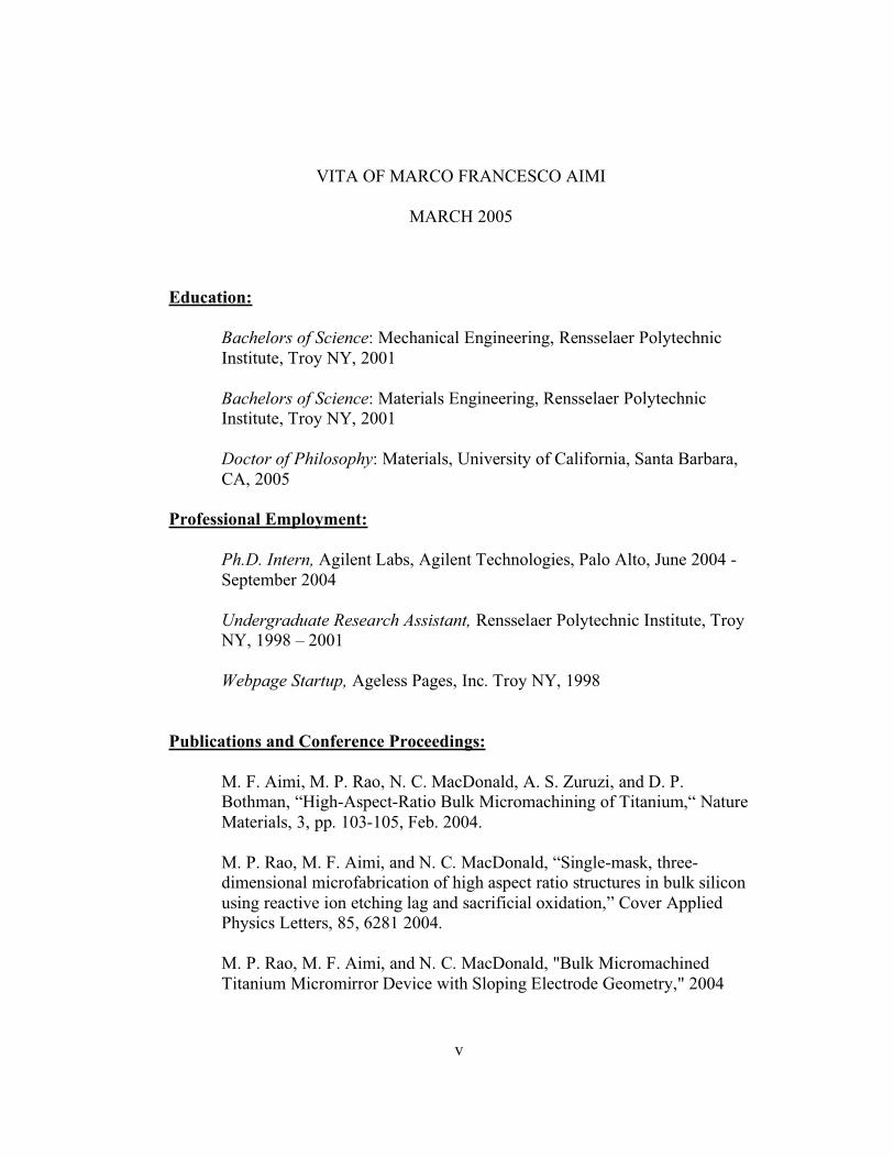
Petersburg, FL.) resulted in the following titanium etch shown in Figure 2.2.
Figure 2.2: Etched titanium substrate using Cl2 gas with a PECVD silicon oxide etch mask
This etch showed that chlorine could be used to etch bulk titanium,
however there are many issues that are very apparent from Figure 2.2. First, there
is a significant amount of undercutting where the masking layer overhangs the
underlying titanium forming a lip. This undercut limits the minimum feature size
of the etch because line widths less than twice the undercut length will be

23
completely removed. Another issue with this etch is the etch damage, which can be
seen by the pockmarks on all of the etched sidewalls. Such etch damages decrease
the mechanical integrity of the beams, particularly if they eventually become free
standing. In addition, the effect of the high residual stress due to the PECVD
silicon oxide, not shown in Figure 2.2, can cause undesired deformation of these
beams upon release. This stress is caused by both the growth stress of the high
temperature PECVD silicon oxide deposition, as well as the large mismatch in the
coefficient of thermal expansion between silicon oxide and titanium.
In order to better understand how these issues change with etch time, in
particular the rate of undercutting, an experiment was run to track these changes
over time. A bulk titanium substrate with a silicon oxide mask was etched using a
chlorine plasma, then placed in an Scanning Electron Microscope (SEM) to
observe the amount of undercut. The substrate was then placed back in the etch
chamber and etched again using the same chlorine etch. By analyzing the etch
results after each step, the lateral etch rate should have been obtainable, however
this was not possible. The lateral etching stopped after each removal of the
titanium from the etch chamber resulting in Figure 2.3. The halting of the lateral
etch rate is of great interest because it is one of the key components in the
development of an etch to match the properties of the silicon deep etch. Several
experiments were run to better understand the cause of this effect, which pointed
to oxygen exposure being the root cause of this sidewall passivation.

24
Figure 2.3: SEM of etch after repeated exposure to room atmosphere during the etching
process.
To verify this effect, an attempt was made to duplicate this sidewall
passivation, this time keeping the titanium in the etch chamber. The same effect
from successive removals of the titanium foil from the chamber was achieved by
cycling between the etch plasma and an oxygen plasma. Decreasing the etch time
from the conditions used to produce the etch shown in Figure 2.3 and running for a
higher number of cycles, the etch shown in Figure 2.4 and Figure 2.5 was
achieved.
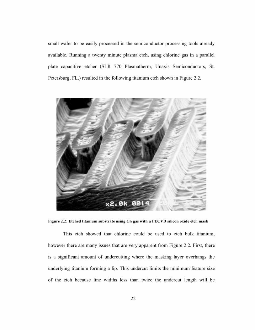
25
Figure 2.4: Comb fingers of the first titanium deep etched structure
Figure 2.5: First cycling titanium deep etch: note the tall grass like features on the surface.

26
From Figure 2.4 and Figure 2.5 it is possible to see the beginnings of a titanium
deep etch process that is capable of forming high aspect ratio structures. It is also
possible to see from the above figures that there are many tall thin structures in the
etched floor. This effect is commonly known as “grassing” or “micromasking” and
can be caused by many different processing issues and impurities from both
semiconductor processing [4] and titanium foil processing. Most of the grassing
from this etch was eliminated by increasing the quality of the polish, increasing the
amount of argon in the plasma and also over etching the oxide mask to ensure no
residual masking material remained on the surface.
The selectivity of the silicon oxide mask to the titanium, measured to be
5:1, was adequate for this etch, but is a not near the selectivity of the Bosch etch,
which is upwards of 200:1. After several attempts to improve the selectivity by
altering the etch conditions, it was decided to develop a new masking material for
the titanium deep etch. Since titanium oxide was resilient enough to prevent lateral
etching, it was expected that this material would also act as a good mask. The
method chosen to deposit the titanium oxide was reactive sputtering, where a
titanium target is sputtered in an argon and oxygen environment, causing the
titanium to oxidize in transit and be deposited on the substrate. During the
development of this process, many samples were run by varying pressure, argon
and oxygen flow rates, power and time. The final deposition conditions were
27
chosen to maximize the deposition rate while maintaining material with high
enough quality to act as an adequate mask.
Along with a method of depositing titanium oxide, the titanium oxide
needed to be plasma etched. Wet etching would not be an option for this case, due
to the risk of undercutting. As a first attempt the same etch condition used to etch
silicon oxide was used to etch the sputtered titanium oxide. This worked the first
time with the only change being a decrease by a factor of 5 in the overall etch rate
of the film. Aside from this drawback, the etch proved to be adequate and even
allowed for the patterning of sub-micron features into the oxide.
With these improvements, the titanium deep etch process was approaching
the performance criteria from the silicon equivalent Bosch process, so it too also
deserved a name. The term Metal Anisotropic Reactive Ion etch with Oxidation
(MARIO) Process [5] was coined to describe this cyclic process, conveniently
named after the author’s grandfather, Mario. A deep etch using the MARIO
process is shown in Figure 2.6.

28
Figure 2.6: MARIO etched 5 micron wide ridge
2.2 The MARIO Process
The MARIO process begins with an initial etch step in which a small
amount of oxide is preferentially removed from all exposed horizontal surfaces via
highly directional physical sputtering by energetic ions. In areas covered by the
etch mask, this bombardment only results in a small reduction of the mask
thickness. In contrast, this sputtering process completely removes the thin oxide in
unmasked areas, therefore exposing the underlying titanium to chemical etching by
the highly reactive chlorine ions in the plasma. The oxide on the sidewalls is not

29
physically sputtered due to the low energy interaction of the ions with the sidewall
keeping the underlying titanium protected from exposure to the chlorine ions.
The duration of the etch step is intentionally limited to only allow a small
amount of etching to take place and is immediately followed by a short exposure
to the oxidation plasma, which grows a new thin protective oxide on all exposed
titanium surfaces. Subsequent cyclic repetition of the etch and oxidation steps
yields highly anisotropic etching of all unmasked areas, therefore allowing for the
definition of HARS. A schematic of the MARIO process is shown in Figure 2.7.

30
Figure 2.7 Process diagram of the MARIO titanium deep etch.
Mask undercutting is reduced significantly in the MARIO process because
of the short duration of the etch step and sidewall protection afforded by the oxide,
allowing for definition of vertical, but corrugated, sidewalls. This corrugation, also
known as “scalloping”, is common to cyclic etch/passivation processes and results
from the slight isotropic nature of the etch step. Altering the oxidation plasma
conditions can change the quality and thickness of the grown oxide, which in turn
changes the amount of protection offered during successive etching steps. The
angle of the sidewall and degree of scalloping can be altered by changing the time

31
of the oxidation and etch step. Increasing the etch time increases the amount of
scalloping, but can also be used to create reentrant sidewalls, i.e. sidewalls that
slope inwards, thus slightly undercutting the etch mask. Decreasing the etch time
can create vertical sidewalls and also decrease the amount of scalloping.
Currently, the process is operated in a Plasmatherm, SLR770 (Unaxis
Semiconductors, St. Petersburg, FL) capacitively coupled plasma etcher. The etch
step is run with a mixture of chlorine (45 sccm) and argon (15 sccm) operated at a
pressure of 23 mTorr with a power of 220 watts. The most commonly used etching
time is 2 min 30 s, which achieves vertical sidewalls with an acceptable overall
cycle etch rate. The oxidation plasma is run directly after the etch plasma with
oxygen (50 sccm) at a pressure of 23 mTorr with a power of 10 watts for 10 s.
Increasing the oxidation time above 10 seconds does not affect the etch greatly,
but reduction below 10 seconds causes breakdown of the protective sidewall oxide
resulting in pitting of the surface. These two plasma conditions are cycled one
after another until the desired depth of the etch is achieved. Depending on the
condition of the etch chamber, a pump down may be necessary between both the
etch and oxidation cycle. This reduces the reflected power in the matching network
and allows for removal of the previous etch chemistry before the following plasma
is struck. The MARIO process also allows for the creation of notches in the
sidewall by changing the etch time during a single loop. Increasing the amount of

32
etching in a single loop, more isotropic etching can occur notching the surface, as
shown in Figure 2.8.

33
Figure 2.8 MARIO deep etch with an extended chlorine etch during the last step used to
partially undercut the beam.
Figure 2.9 4 micron wide titanium beam deep etched using the MARIO process.

34
Figure 2.10 MARIO etched non-released titanium comb drive actuator.
2.3 Baseline Titanium Deep Etch Process
Titanium deep etching begins with commercially pure titanium substrates
with thickness ranging from 10 to 500 microns. Owing to the greater toughness of
titanium relative to silicon, free-standing substrates thicker than 25 microns can be
processed without the need for backing or carrier wafers. Titanium substrates
thinner than 25 micron are generally too compliant to support their own weight,
and thus require extra support to prevent kinking from handling. This support is
normally provided by temporary adhesion to a handling wafer.
The titanium substrates used thus far are rolled annealed sheet-stock with
as-received surface roughness in excess of 150 nanometers RMS. Therefore, they

35
generally require polishing to enable subsequent optical lithographic patterning.
Process development to optimize the polish has shown that a single step chemical-
mechanical polishing process using colloidal silica is often sufficient to reduce the
fine-scale roughness that otherwise interferes with high-resolution lithography.
Typically, polished substrates have a surface roughness less than 50 nanometers
RMS.
Following the polish, a titania etch mask is deposited on the titanium
substrate by reactively sputtering titanium from a DC target in an oxygen/argon
environment using the Endevor 3000 (Sputtered Films, Santa Barbara, CA) cluster
sputter tool. The optimal flow rates for oxygen and argon are 10 sccm and 20
sccm, respectively, which achieve a process pressure of 3.7 mTorr. A power of 2.2
kilowatts for 1 hr 15 min. achieves a 1.2 micron titania film.
The titania-coated titanium substrates are then patterned using standard
photolithography techniques with a reproducible minimum feature size of 1.25
microns. The patterned and developed photoresist is used as an etch mask for the
underlying titania layer that is etched using a standard silicon oxide plasma etch
using the Panasonic E640 (Osaka, Japan). The titania etch has a high selectivity to
bulk titanium because it is a fluorine based plasma. The etch process consists of
CHF3 (40 sccm) as the etch gas with an ICP and bias power of 500 W and 400 W
for 9 min 30 s at a pressure of 1 Pa.

36
Once the titania etch mask has been defined, the titanium substrate is deep
etched using the MARIO process, which is shown earlier to be a cycling plasma
etch that alternates between short exposures to an etching plasma and an oxidation
plasma to yield HARS in bulk titanium. The etch plasma is fed by a combination
of chlorine and argon gases operated at high power, while the oxidation plasma is
pure oxygen and operated at low power. The process outlined here is just a
baseline titanium deep etch and are the minimum required steps to deep etch bulk
titanium.
2.4 Undercutting Titanium Structures
Undercutting structures is a common technique used in the fabrication of
many silicon based MEMS devices. It was initially assumed that any titanium
MEMS device would have to use an undercutting process to create movable
structures. Undercutting is a process in which material below a previously deep
etched beam is removed using an isotropic etch, where the amount of lateral
etching is approximately equal to the amount of vertical etching. An example of
such a process that utilized undercutting is the Single-Crystal Reactive Etching
And Metallization (SCREAM) process shown below in Figure 2.11 [6].

37
Figure 2.11 Single Crystal Silicon Reactive Ion Etch And Metalization (SCREAM) process in
silicon. 1) Deposit or grow silicon oxide. 2) Pattern photoresist 3) Transfer pattern to oxide
mask 4) Remove photoresist 5) Deep etch silicon 6) Deposit CVD oxide 7) Anisotropically etch
oxide 8) Deep etch silicon to extend the floor 9) Undercut silicon using an isotropic etch 10)
Sputter deposit metal [6].
This process is misleadingly simple. Assuming a non-directional
bombardment of ions on the titanium surface, the resulting etch will be non-
directional. This is true of the Bosch process where the silicon etch plasma is
inherently non-directional and a polymerization step is necessary to achieve an
overall anisotropic etch. This is not the case for the MARIO etch, which was
developed in a parallel plate plasma etcher where in order to sustain a plasma, a
directional bias must be generated between the surrounding electrodes and
substrate. This limits the etch to be mostly anisotropic and can cause great
difficulty in undercut structures.

38
Several attempts were made to try to generate an isotropic etch, raising the
pressure, decreasing the RF power and decreasing the concentration of argon in the
plasma. There were a few etches that were re-entrant which, when run for a long
enough period of time, were successful in undercutting narrow structures.
However, such an etch is not very useful when trying to create high quality MEMS
devices. An example of such an etch is shown in Figure 2.12.
Figure 2.12 Partly released titanium beam with a poor undercut.
From Figure 2.12 it can be seen that this undercutting process is not
practical because it forms very sharp release points and sidewalls with a lot of
damage. There was no success undercutting using this technique, therefore other

39
methods of releasing titanium had to be explored to enable the fabrication of
movable MEMS.
2.5 Thin Foil Processing
With the difficulty in releasing titanium MEMS, another approach for
creating moving structures was taken. Due to the mechanical properties of titanium
it is possible to process very thin foils (10 micron foils are used in the micro-
mirror device explained later in this dissertation). With the titanium deep etch
process, thin foils are able to be through etched and processed just like their
thicker counterparts. These thin foils can be also be bonded onto other structures to
create released devices with the added benefit of being able to fabricate MEMS
with more design flexibility. This simple idea has allowed for the fabrication of all
of the devices presented in this dissertation and is a solution to avoid inadequate
process techniques to achieve an undercut. Details of this process will be explained
in Chapter 3.
2.6 Micromasking
Micromasking, or grassing, is a significant issue in bulk MEMS and is a
critical issue in bulk titanium MEMS. Grassing occurs due to the introduction of
an impurity with a slower etch rate than the base substrate, causing a small area to
etch slower than of that the surrounding field. Sometimes this grassing is so great,
it will slow the etch rate to zero. SEM images of these samples show very fine

40
spikes or hairs coming off the surface, very similar to a well cultivated lawn, hence
the term “grass”.
Figure 2.13 SEM image of micromasking during the deep etch of a comb drive.
It is not the intent of this research to determine the full reasoning for grassing or
develop solutions to this problem, but it is an important component to the deep
etching of titanium. Several different conjectures exist that explain the presence of
grass in some titanium samples. It has been noticed in thick samples with large
grains, that grassing occurs at grain boundaries. For thinner samples with smaller
grains, the grass occurs everywhere. The explanation proposed is the migration of
impurities, such as iron or oxygen, to the grain boundaries which micromask
during the deep etch. Another possibility is the existence of retained beta phase at

41
the grain boundaries from heat treatment. Either explanation needs to be
investigated with the aid of the titanium producer to achieve a solution.
2.7 Summary
Using the silicon deep etch as a baseline process, a titanium deep etch has
been developed that also uses two different plasma chemistries, but instead of an
etch/passivation cycle the titanium etch is an etch/oxidation cycle. Along with the
titanium deep etch, other process developments were made to enable lithography
and oxide etching on titanium substrates. All of the newly developed processes
allow for the etching of titanium using standard semiconductor equipment

42
References
[1] Laermer, F., Schilp, A., Bosch, R. Method of anisotropically etching
silicon. US Patent No. 5501893.
[2] www.stsystems.com (2005).
[3] Blumenstock, K. Stephani, D. Anisotropic reactive ion etching of
titanium. J. Vac Sci. Tech. B. 7 627-32. (1989).[4] Perera, A.H., Satterfield, M.J. Micromasking of plasma etching due to
bacteria: a yield detractor for ULSI. IEEE Transactions onSemiconductor Manufacturing 9 577-80 (1996).
[5] Aimi, M.F., Rao, M.P., MacDonald, N.C., Zuruzi, A.S., Bothman, D.P.
High-aspect-ratio bulk micromachining of titanium. Nature Materials.
3 105-5 (2004).
[6] K.A. Shaw, Z.L. Zhang, N.C. MacDonald. SCREAM I: a single mask,
single-crystal silicon, reactive ion etching process for
microelectromechanical structures. Sensors & Actuators A 40 63-70
(1994).

43
Chapter 3: Titanium Device Development
With the development of the titanium deep etch and other bulk titanium
processing techniques, it is possible to consider fabricating the first bulk titanium
MEMS device. Many different titanium devices are exciting when considering the
very different set of newly available material properties. Biological, high shock
and large array type of devices are of interest because of the unique properties of
titanium. It is also possible to evaluate traditional MEMS devices using the new
processing techniques such as thin foil stacking. This is the approach taken when
choosing to fabricate an array of micro-mirrors.
For an initial attempt, a simpler version of a micro-mirror is created to
better understand the processing specifics for the fabrication of a mirror device.
This first attempt of a bulk titanium MEMS device is called the macro-mirror
device because the mirrors created are over one square millimeter with 10 micron
wide torsion bars used as restoring springs.
3.1 Macromirror Array
A 2 x 2 mirror array is fabricated by taking advantage of thin titanium foil
processing. Three layers are used in this device, the first being a 25 micron thick
foil that is deep etched to create the released mirror and torsion springs, the
second, a 30 micron thick foil is wet etched to create a square through hole that
will be placed under the mirror and finally, the silicon substrate is oxidized and
metalized creating isolated electrodes. By bonding these three layers together

44
using gold to gold thermal compression bonding, the metal stack can operate as a
macro-mirror device. This device is operated through electrostatics and is actuated
by applying a voltage across the air gap from the underlying electrode and the
underside of the mirror surface. A schematic of the layers and final device are
shown in Figure 3.1 and Figure 3.2.
Figure 3.1 Schematic of the separate layers for an element of the macro-mirror device. Top
layer is the through etched mirror pattern, second layer is the spacer foil and the final layer is
the electrode layer.

45
Figure 3.2 Schematic of a single bonded element of the macro-mirror device.
3.1.1 Fabrication of the Macro-Mirror
The fabrication process for the macro-mirror is relatively simple due to the
design and large feature sizes, making it a good choice for the first bulk titanium
MEMS device. The process shown here shows some of the strengths and
flexibility of processing titanium. To better explain the process, it is broken into
three sections, one for each layer. All of the processing is done using an Endevor
3000 sputter cluster tool, a SRL770 Plasma Etcher, a MJB 3 UV400 contact
aligner (Suss Microtec, Waterbury, VT), a MRC 51 Plasma etcher (Praxair,
Danbury, CT), SEC600 E-Beam Evaporator (CHA Industries, Fremont, CA) and a
M-8A flip chip aligner bonder (Research Devices, Piscataway, NJ).

46
3.1.1.1 Mirror Layer
In order to create the released mirror and torsion bars, the titanium foil
needs to be through etched. Along with the deep etching, a gold layer for gold
thermal compression bonding needs to be deposited on the backside of the foil.
This gold layer is patterned only on the supporting structure of the mirror to
prevent this gold from coming into contact with the metalized electrode during full
tilt of the macro-mirror. This is done to prevent stiction between two gold surfaces
that is traditionally problematic for MEMS .
A rolled and annealed 25 micron thick titanium foil is obtained from
Goodfellow corporation (Lancaster, PA) to fabricate the top layer. For this
process, no polishing is required because the minimum feature size is 10 microns,
which can be defined using the contact aligner even on the as-received surface
roughness of the foil. Using a similar process flow to the titanium deep etch
explained in Section 2.3, a sputtered titanium oxide film is deposited onto the
titanium foil. This etch mask is patterned using a photoresist mask and an oxide
etch. After stripping the photoresist from the front side, the backside of the foil is
patterned using photoresist designed for lift off.
Due to the limitations of the contact aligner, direct alignment from the
backside of the foil to the front side is not possible. In order to circumvent this
issue, a secondary alignment is performed using the edges of the titanium foil as
alignment marks. This alignment is preformed using two lines on the outskirts of

47
the mask field that is transferred into the oxide mask. Scissors are then used to cut
the foil along these two lines, making the new edge of the foil a known distance
from the front side pattern. These two new edges are then used as alignment marks
for aligning the backside liftoff pattern to the front side deep etch pattern. This
method is successful for this large device because the features are very large and
the tolerances for alignment are +/- 300 microns which can easily be achieved
using a good pair of scissors and steady hands.
After the backside liftoff mask has been defined, a layer of titanium and
gold are deposited using an E-beam evaporator. The titanium layer is 100
nanometers thick and is used for an adhesion layer, while the much thicker gold,
500 nanometers, is used for thermal compression bonding. The thick gold layer
allows for flow to occur at the bonding pressures and temperatures. With the gold
deposited, lift off is performed by soaking the foil in acetone. For best results, no
ultrasonication is used due to the tendency for the removed gold film to cold weld
to the other gold and titanium surfaces.
After an additional clean in acetone and isopropanal, the foil is placed with
the oxide mask facing up into the chlorine dry etch system for the MARIO
process. The etch conditions used are the same conditions presented perviously for
a total time of 2 hrs. This through etches the foil, releasing the mirrors with only
the torsion bars holding the mirror in pluptateace.

48
Figure 3.3 Dark field mask layout of the macro-mirror for the upper titanium foil
Figure 3.3 shows a dark field mask of the macro-mirror where the shaded sections
will be through etched. The mask layout shows the center clear section that defines
the macro-mirror, while the enlarged section shows the anchor between the mirror
and the torsion spring.
3.1.1.2 Spacer Foil
The spacer foil is fabricated from a 30 micron thick titanium foil. This foil
is wet etched with a square pattern to allow for a raised bond surface for the mirror
supports. A wet etch is chosen because it is faster than dry etching and the lateral

49
etching, consistent with most wet etches, is allowable. To make the spacer, the
foils are patterned with photoresist making an exposed square and covered
surroundings. The backside of the foil is then also covered in photoresist to
prevent the backside of the foil from being etched. This foil is then etched in a
10:1 DI water: HF solution for 5 min or until all of the titanium is removed from
the exposed hole. After removing the photoresist, 100 nanometers of titanium and
500 nanometers of gold are deposited on both sides of the spacer using an E-beam
evaporator.
3.1.1.3 Electrodes
The electrodes for this device are created from a silicon wafer due to the
ease of electrically isolating each of the electrodes with thermal oxide. Using a
liftoff process, thin films of 100 nm of titanium and 500 nm of gold are patterned
on to a silicon wafer with 1 micron of thermal oxide. The pattern consists of two
electrodes and a thermal compression bond region. The light regions of the dark
field mask shown in Figure 3.4 define the locations of the deposited titanium and
gold.

50
Figure 3.4 Dark field mask layout of the macro-mirror for the silicon substrate.
3.1.1.4 Bonding
Using the maximum settings on the flip chip bonder of 10 Kg and 350OC
for a bond time of 3 minutes, the electrode die and spacer foil are bonded together.
After cooling, the top foil containing the mirrors is bonded onto the electrodes and
spacer foil using the same bonding conditions. SEM micrographs of the macro-
mirror device are shown in Figure 3.5 and Figure 3.6.

51
Figure 3.5 SEM of the final bonded macro-mirror with the mirror suspended above the
electrodes by a gap height dictated by the spacer foil thickness of 30 microns.
Figure 3.6 Enlarged image of the torsion spring of the macro-mirror.

52
3.1.2 Testing of the Macro-Mirror
Some of the basic mechanical properties of bulk titanium MEMS can be
investigated using this simple torsional mirror device. By fabricating this device,
concerns over releasing structures from a titanium foil were suppressed. The
released mirror remained in plane with the surrounding frame, even with it only
being supported by thin torsion bars. The mirror surface also is not detectably
warped during the release and bonding of the foil. Other questions about the
mechanical integrity of the device can be answered through actuation of the
device, mainly observing if the endurance limit assumption remains valid on this
length scale. To test this assumption, the device is cycled using electrostatic
actuation.
Grounding the mirror foil and applying a voltage to one of the underlying
electrodes actuates the mirror. The degree of mirror rotation can be controlled with
the applied voltage up to the point where the upper mirror reaches its instability
and snaps down to the electrode. The velocity response of the system under
conditions with and without snap down at a 25 microsecond pulse width and 50%
duty cycle can be seen in Figure 3.7. The measurement shown in this figure is
made with a Polytec Laser Doppler Vibrometer (Polytec PI, Aubum, MA) that
uses the Doppler shift between the incident light and reflected light to measure the
velocity of the measured surface. The laser for the vibrometer is passed through an
optical microscope to allow the measurement of MEMS devices. This device is

53
measured at the farthest point on the mirror surface from the torsion bar, giving the
maximum velocity of the device. From the measurements, it can be seen that the
device behaves like an over damped system with a very slow response time due to
the huge torsional mass and compliant springs.
Figure 3.7 Time response of the macro-mirror to two different amplitude step inputs.
Despite the poor dynamic performance of this device, it does show a few
aspects of bulk titanium MEMS and can be used to answer some of the basic
mechanics and materials questions. It is of interest to note that the mirror does not

54
show problems with stiction even at one million snap down cycles and also does
not short when the mirror is in direct contact with the electrodes. The large lifetime
of the torsion springs is consistent with the macro properties of titanium, having a
modeled stress amplitude of only 16 MPa, which is below the endurance limit for
titanium. The lack of shorting is anticipated to be due to the poor quality of the
through etch on this device. During the fabrication process, the etch is timed to
stop only when the large features are fully etched. This caused sections near the
walls to still have thin strands of titanium that are expected to have oxidized
through. These strands can be seen in the SEM micrograph of Figure 3.6 by the
white hair on the bottom side of the mirror and spring. It is proposed that these
hairs are what touch the gold electrodes during the snap down cycle and prevent
the mirror from sticking to the surface.
The macro-mirror array shows how the developed titanium fabrication
processing techniques are used to make the very first bulk titanium MEMS. It also
shows the potential of making torsion based titanium MEMS with the ability to
achieve large number of cycles without failure.
3.2 Micro-mirror Array
The results of the macro-mirror array lead way to proposed research for a
micro-mirror array for an optical delay path system being developed at another
university. The specifications for this array are listed in Table 3.1.

55
Table 3.1 Design specification for the micro-mirror device.
• 10 x 10 mirror array• 100 x 100 µm mirror size• 250 µm distance between mirrors• Turn on voltage less than 100 volts
• Response time < 500 µs• Three position mirror with -10, 0, and +10 degree tilt
• Half the mirrors tilt north-south, other half east-west
In order to reach these design parameters, several new processing
techniques needed to be developed. The state of the art after development of the
macro-mirror device limited feature sizes to 10 micron, which would be too large
to meet the desired requirements of mirror pitch. Along with the need for better
process control, new mirror designs needed to be investigated to keep a fast
response time, but also maintain a low drive voltage. With the fixed requirements
of each micro-mirror being able to swing to both +10 and -10 degrees and a fixed
mirror size, not much can be done to reduce the drive voltage with a design similar
to the macro-mirror device. The torsion springs can be redesigned to be more
compliant, but this will cause an increase in the response time because of the
lowered resonant frequency. To decrease the drive voltage but maintain adequate
response time, another electrode design was developed.
3.2.1 Electrode Development
In order to improve the drive voltage without altering the response time, a
new electrode design is necessary to increase the electrostatic force but still

56
maintain the +/- 10 degree maximum angle. The proposed solution is to make
three-dimensional electrodes that slope downward from the mirror centerline to the
edge, decreasing the air gap between the electrode and mirror, but still allowing
the maximum tilt angle, resulting in a decreased drive voltage. A schematic of both
the flat electrode design and the sloping electrode design are shown below in
Figure 3.8.
Figure 3.8 Schematic of the sloping and flat possible electrodes for the micro-mirror array.
3.2.1.1 Analytical Reasoning for Sloping Electrodes
An estimate of the reduction in drive voltage can be calculated by
analyzing the electrostatic force and restoring mechanical force for both a flat and
sloping electrode. Assuming the mechanical stiffness of the beam is linear within
the deflection during normal operation, the restoring mechanical torque can be
determined.
Tm = K�� 3.1
Where,

57
K� =2Gab3
3L1�192b
� 5aTanh
�a
2b
�
��
�
�
�
�
�� [1] 3.2
Valid for b < a
Where a is the beam height, b is the beam width, L is the beam length and G is the
shear modulus of the beam material.
The electrostatic torque generated from the backside of the mirror to the electrodes
can be determined by integrating the differential area across the whole mirror,
tracking the gap between the mirror and electrode.
Figure 3.9 Schematic of the mirror device showing pertinent geometry.
The gap initial length, d, can be determined by the following.

58
d = go Cos �( ) 3.3
Knowing capacitance and thus the force along each delta x, the total applied torque
can be determined by integrating the differential torque from the inner edge of the
electrode to the outer edge of the electrode.
Te = x�0wV
2
2 d + x Tan � ��( )( )2
�
�
��
��dx
xo
xe +xo
� [2] 3.4
Where � is the permittivity of air, w is the width of the electrode, V is the applied
voltage and � and � are the angle of the electrode and mirror respectively.
Plotting both the torque applied by the electric field and the restoring torque, the
instability voltage to cause the mirror to snap to the electrode can be determined.
Two examples of the torque versus mirror angle are shown in Figure 3.10 and
Figure 3.11, where 70 volts gives a stable mirror tilt angle of 1.7 degrees, but at 87
volts the maximum stable solution is obtained of 4.5 degrees. Any voltage above
this will cause snap down. Both of these solutions use the geometry in Table 3.2.

59
Figure 3.10 Electrostatic applied torque and mechanical restoring torque at 70 volts for
various mirror tilt angles. Results show a stable and unstable solution for the mirror angle.

60
Figure 3.11 Electrostatic applied torque and mechanical restoring torque at 87 volts for
various mirror tilt angles. Results show a single stable solution being the maximum mirror
tilt before snap down.
Table 3.2 Geometry used in the above calculations of the minimum voltage for snap down.
Variable g0 xo xe wm � a B L
Length (microns) 0.9 5 44.25 100 10 deg 10 1.0 60

61
Using the same formulation, but for a flat electrode with �=0 and g0=8.68 microns
to give a 10 degree final slope, the snap down voltage is 152 volts. By using the
geometry of a sloping electrode verses a flat electrode for the mirror design, the
driving voltage is reduced by 43 percent. This decrease in voltage is done without
sacrifice of the device response time, increasing the possibility of reaching the
design criteria.
3.2.2 Electrode Fabrication
The processing of three-dimensional electrodes is not as easy as first
anticipated. After considering resist reflow and using the Focus Ion Beam (FIB) as
a fabrication tool, the proposed solution to make three-dimensional electrodes is to
use Reactive Ion Etching (RIE) lag to produce different height structures. RIE lag
is an effect characterized by a decreased etch rate with the increased aspect ratio of
etch holes [3]. This etching effect is normally considered a corollary due to the
decreased gas transport into and out of a deep trench, but it is possible to utilize
this effect by patterning small vias causing significant lag.
A good example of RIE lag in a silicon deep etch is shown below in Figure
3.12, where a series of trenches are etched with continuously decreasing gap
spacing from right to left.

62
Figure 3.12: Example of RIE lag in silicon from the Bosch Process (cross sectional view
shown).
From the cross section above it is possible to see that the floor of the etch in the
narrow trenches is etched less than in the wide, open area. This lag effect can be
accentuated even more by defining square vias, not just trenches, allowing
variation in etch depth up to 10 micron for a 22 minute etch. With this process,
almost any height variation can be fabricated just by changing the size of the etch
via. Thus, by making a gradual transition from large to small vias, a sloped
structure can be fabricated. A mask layout for this process is shown in Figure 3.13,
where two sloping electrodes are fabricated along with the interconnect wires and
bond frame.

63
Figure 3.13 Light field mask for the electrode pattern that utilizes the RIE lag effect.
Since the floor of the etch is the only interest from the deep etch, the via
frame needs to be removed. In silicon, it was realized the best method for this
process is to oxidize all the way through the frame, then use hydrofluoric acid to
wet etch off all of the formed oxide. The oxidation process for silicon is quite slow
when compared to the deep etch, allowing full gas transport into and out of the
etched vias resulting in a consistent thin film of oxide grown over the whole via
frame and etch floor. Subsequent wet etching in HF removes this oxide, but is
highly selective to the underlying silicon, which allows for over etching with out
risk of removing any non-oxidized silicon.

64
It was quickly learned that there is a significant problem with this process
if all of the oxidation is preformed in one step. The volume expansion of the
oxidized silicon in the via frame causes enough stress to plastically flow the silicon
under the frame at the oxidation temperature, causing the silicon to warp out of
plane. An example of this processing induced stress can be seen in Figure 3.14,
where the stress due to oxidation causes the bond frame to bow out of plane. This
effect is best seen on the bond frame sidewall, which is no longer vertical.

65
Figure 3.14 Cross section of electrodes after deep etch and single oxidation step. Notice the
bowing in the bond frame.
In order to eliminate this problem, the oxidation and wet etching processes
are cycled. After the deep etch, the wafer is oxidized to grow 300 nanometers of
oxide then wet etched in HF to remove the grown oxide, followed by another 300
nanometers of oxide and wet etch. Running through this process for approximately
8 cycles, all of the deep etch frame is removed leaving only the etch floor with no
out of plane bowing, verified using the Wyko 1100 white light interferometer
(Veeco, Woodbury, NY).

66
Along with the formation of the sloping electrodes, other three dimensional
structures necessary for the micro-mirror device are formed using the same
process. These elements consist of a bonding frame, to allow the mirror foil to be
bonded onto the electrode die without the use of a spacer foil, and electrical
interconnects that run under the mirror foil from the electrodes to bond pads. The
nature of the process makes it possible to create all three elements; electrodes,
bond frame and interconnect lines all at the same time using the same process,
even though all three elements require different heights [4]. A schematic of the
deep etch and oxidation process is shown in Figure 3.15.

67
Figure 3.15 Schematic of the deep etch, oxidation and wet etch processes used to fabricate the
sloping electrodes, interconnect lines and bonding frame in silicon.
With the silicon wafer in the desired topology, electrical isolation between
each of the electrodes and bond frame needs to be created. This is done by
oxidizing the wafer for the final time, growing a 500 nanometer oxide on all of the
surfaces. Then by taking advantage of the deep etched structure, gold is deposited
anisotropicaly by E-beam deposition, which allows for the majority of the gold to
be deposited on horizontal surfaces, but not on vertical surfaces because of the
directionality of the deposition. This is then followed by a brief gold wet etch used

68
to remove any electrical shorts that may exist due to gold deposition on the
sidewall, which is possible since the gold wet etch is isotropic. Different sections
of the electrode device are shown in the following figures. A SEM image of the
array is shown in Figure 3.16, while a close up of one of the elements is shown in
Figure 3.17. It can be seen from this figure that there is no retained gold on the
sidewall of the structure exposing the silicon oxide. Finally, the last figure, Figure
3.18, shows the termination of the interconnect lines out to wire bond pads. From
all of these SEM micrographs it is possible to see texture on the gold surface, this
is due to the oxidation of the via frame that results in bumps wherever there is a
crossing point in the frame. This texture does not hinder the future bonding steps,
but may have negative implications when dealing with issues of stiction.

69
Figure 3.16 Array of sloping electrodes also showing the bond frame and interconnect lines.
Figure 3.17 Single sloping electrode covered in gold. Notice the lack of gold on the sidewalls.

70
Figure 3.18 Bond pads on the perimeter of the die used to wire bond into the package.
After all of the fabrication is performed, the wafer is divided into each die
by dicing a cleave line into the wafer along the perimeter of each of the die. A
thick layer of photoresist covers the entire wafer to protect it from damage and
shield the surfaces from debris during dicing. After dicing, the resist is removed
and each die is singulated.
3.2.3 Mirror Development
Focusing on the mirror, new handling and processing techniques are
required to further the development process of the 10 micron thick foils with 1.5
micron wide springs, a necessity to meet the given design requirements.
Processing foils less than 25 micron thick proves to be difficult because of their
tendency to kink or fold. The higher stiffness of the 25 micron thick foils allows

71
the spinning of the whole 1 inch square foil on a resist spinner without any
kinking. In contrast, 10 micron thick foils required attachment to a carrier wafer
during most of the processing steps. Typically, the carrier wafer is silicon and the
attaching adhesive is a thin layer of diffusion pump oil that allowed adequate
adhesion and thermal conduction while also allowing for the necessary removal of
the foil after the processing.
The reduction of the minimum feature size also required further process
development. Differing from the macro-mirror device, lithography with the stepper
is required to expose 1.5 micron features in photoresist, thus a polished titanium
substrate is necessary to accept these micron features. Initial lithography tests
without polishing caused the photoresist to peel or fail during the development of
small features. An example of this is shown below in Figure 3.19, where the
photoresist peeled in such a way to create an arch where the torsion spring pattern
is exposed. This effect is most likely due to a rough surface that can scatter the
exposed light, causing thinning and undercutting of the resist profile.

72
Figure 3.19 Mirror pattern on unpolished titanium where thin segments of the photoresist are
peeled up from the surface.
In order to achieve smaller feature sizes during photolithography, a
polishing technique was developed and the final optimized process presented here.
This process begins with the mounting of the 10 micron foil onto a polishing puck
for the Allied High Tech MultiPrep System (Allied High Tech, Ranncho
Domingues, CA). After an adequate bond, the thin foils are polished in a 0.2 µm
colloidal silica slurry on a “red final C” CMP cloth from Allied High Tech. After
20 min of polishing under the highest load at a speed of 120 RPM, the foil is
removed and placed in micro organic soap from Allied High Tech. The soap

73
allows the silica particles to be removed from the surface with best results
achieved using ultrasonication. As a point of caution, ultrasonication under high
powers caused the foil to curl, destroying the sample.
After polishing, a lift off structure, shown in Figure 3.20 by the striped
layer, is patterned onto the foil using stepper lithography. Along with the lift off
structure, alignment marks are also deposited onto the foil (different from the
macro-mirror array, the micro-mirror array process is all done on one side of the
wafer to eliminate the need for backside alignment). With this lift off pattern,
titanium and gold are deposited onto the foil in the same manner as the macro-
mirror device. After liftoff in acetone and isopropanal, titanium oxide is sputtered
onto the entire surface covering the bare titanium and gold film. Next, the mirror
pattern is exposed onto the foil using the alignment marks from the previous gold
lift off, which are visible through the sputter oxide film. Using this pattern, the
oxide is etched with the standard titanium oxide etch then cleaned in an ultrasonic
bath of acetone then isopropanal, removing residual photoresist.

74
Figure 3.20 Light field mask of the thermal compression gold layer (dark stripes) and the
titanium oxide mask layer (light squares).
With the masking oxide defined, the foil is deep etched using an optimized
MARIO process reducing the degree of scalloping to improve the minimum
feature size at the sacrifice of the overall etch rate. The titanium is over etched by
50% to ensure a clean sidewall and lower edge, which was not implemented in the
macro-mirror. The deep etch not only releases all of the mirrors, but also releases
each of the mirror die from the foil. Typically, each foil contains 9 to 16 mirror die

75
per square inch and singulating each die with the deep etch avoids the need of
mechanical separation, such a cutting that can cause warping.
After the deep etch, the masking oxide needs to be removed to expose the
gold used in bonding. The fastest way to remove this oxide is to use the ICP
Panasonic E640 etcher, but due to the high power of the etch a good thermal
conductivity from the sample to the carrier wafer is required. This proved difficult
with released devices. In order to avoid over heating, a different tool with a
capacitivly coupled plasma is used to remove the titanium oxide etch mask. The
MRC 51 parallel plate etch tool is used to remove the oxide on the surface with
CF4, which has adequate selectivity to the underlying gold. This tool is lower
power and the sample does not require good thermal conductivity to the platen, so
resting the foil on a silicon wafer is sufficient. The trade off for low power plasma
is a very long etch time, which can be upwards of 6 hours to remove the 1 micron
of masking oxide. Mirrors processed up through the deep etch step are shown
below in Figure 3.21 and Figure 3.22. The spring widths shown here are 1.5
microns with 100% yield over the entire single die.

76
Figure 3.21: SEM image of the free standing micro-mirror etched from a 10 micron thick
titanium foil.
Figure 3.22: Spring support of the micro-mirror showing the scallops due to the cyclic nature
of the MARIO etch.

77
After the long oxide etch, all of the gold on the bond area is exposed. Due
to the lift off pattern, gold is only exposed on the bonding frame and not the
backside of the mirror or torsion bars. Alignment and bonding the mirror die to the
electrode die is performed in the flip chip bonder. With the upper platen modified
to accept a single mirror die, both the mirror foil and electrodes are placed in the
upper and lower platen respectively. After alignment and ensuring parallelism
using the optics of the flip chip, bonding is preformed using the maximum load
and temperature of 10 Kg and 3500C for 3 minutes. This aligned bonding allows
the mirrors to be placed directly over the sloping electrodes, where the gap
between the mirror and top of the electrode is dictated by the gold thickness and
the etch height of the bonding frame. Due to the limitation of the flip chip bonder,
accuracies down to only 2 microns are possible, which is a significant drawback to
this process but can be overcome with better calibration and a better bonder. A
schematic of the final device is shown below in Figure 3.23 and a SEM image of
the final device with one of the mirrors snapped down is shown in Figure 3.24.
Another SEM image showing the wiring of the interconnects entering under the
mirror foil is shown in Figure 3.25.

78
Figure 3.23 Schematic cross section of the micro-mirror with the titanium foil bonded onto
the silicon substrate using thermal compression gold, which is on top of oxidized silicon.
Figure 3.24: Bonded micro-mirror array with one of the titanium mirrors actuated.

79
Figure 3.25 Interconnect lines entering under the edge of the titanium foil.
3.2.4 Package Assembly
With the mirror chip fabricated, it needs to be assembled into a package for
testing under vacuum conditions and other applications where probing is not
convenient. The 208 pin package chosen is a Kyocera Pin Grid Array (PGA) with
a die cavity of 14 millimeters which just fits the total electrode size of 13.5
millimeters. The die is soldered into the package and wire bonds are made with
gold wire from the package to each of the wire bond pads using gold wire. Figure
3.26 shows the attachment of the ball bonds onto the wire bond pads, onto the
gold-coated electrode die.

80
Figure 3.26 Wire bonds attached to the gold coated wire bond pads.
3.3 Testing the Micro-mirror Device
The micro-mirror is driven in the same manner as the macro-mirror device.
A voltage is applied to the underlying electrode while keeping the mirror
containing titanium foil grounded. Each mirror element contains two electrodes,
one to drive it to +10 degrees and another to drive it to -10 degrees, which
correlates to 200 separate signals for the whole device plus one common ground
signal. Applying a bias to an interconnect line will make the correlating mirror
device actuate. Basic testing is done in air by probing the bond pads, but tests

81
under vacuum are completed with the device fully packaged and electrical feeds
running out of the vacuum systems.
Several different aspects of the mirror device can be tested by measuring
both the transient and steady state responses of the device to a variety of input
voltages at different pressures. The main focus of testing for the mirror device is to
determine the settling time, drive voltage and stiction. Other tests are also
preformed to determine the resonant frequency and quality factor that are more of
an interest for future titanium MEMS devices, not necessarily this mirror device.
Initial tests showed that stiction is a major problem for these devices. After
several snap down cycles, the mirror would stick for some period of time, limiting
how these devices can be tested. Several different designs are attempted to avoid
this problem, but it is still a large unresolved issue. In order to work around this
problem, the mirrors are run in analogue/scanning mode limiting the applied
voltage and maximum mirror angle to below the snap down instability. Running
under this mode, the settling time and angle of twist for a given voltage can be
determined.
The settling time, damping coefficient and resonant frequency can be
determined by applying a step input signal. Mirrors with springs 1.25 microns
wide and 60 microns long have a resonant frequency of about 75 kHz, with a snap
down voltage of approximately 75 volts with well aligned sloped electrodes. One

82
of the step responses of a micro-mirror with a 60-volt input signal is shown below
in Figure 3.27.
Figure 3.27 Step response of the mirror device with a comparison to a second order
underdamped system.
The damping for this device is not large and by fitting the response of the mirror to
a second order underdamped resonant system, the damping coefficient of 0.019 is
obtained with a total settling time of 2.7 milliseconds, defined by the time to reach
2% of the steady state value. This settling time is well above the design specs and
alternative device designs need to be investigated for improvement. One obvious

83
solution is to increase the damping in the system either by altering the mirror or
electrode geometry.
Both alterations to the mirror and electrode geometry are made in the next
generation of devices. The open areas in the electrodes are filled in with tall
structures to impede air being pushed by the mirror. Similarly, the gap between the
mirror and surrounding frame is decreased with the similar intent of impeding the
movement of displaced air. Figures of both the electrode and mirror are shown in
Figure 3.28 and Figure 3.29.

84
Figure 3.28 New electrode design with open areas closed in to reduce the settling time of the
mirror device.
Figure 3.29 New mirror design with enclosed area around the springs and mirror platform to
reduce the settling time of the mirror device.

85
Both of these design alterations greatly improve the settling time of the system.
Settling times to a displacement an angle and back to the zero state are shown in
Figure 3.30 and Figure 3.31. The settling time for the mirror to reach 2.5 degrees is
0.60 milliseconds while the time to settle for the mirror to return to the zero state is
0.46 milliseconds. Again, fitting these two responses to a second order
underdamped system, the damping coefficient is 0.312 for the swing to a
displacement angle, while 0.3 for the swing to zero.
Figure 3.30 Step response of the new mirror device to the positive slope of the input signal
compared with a second order underdamped system.

86
Figure 3.31 Step response of the new mirror device to the negative slope of the input signal
compared with a second order underdamped system.
The mirror surface roughness poses an issue with the current micro-mirror
device. The small scale surface roughness and the larger scale surface roughness
decrease the ability to reflect the laser light. Measurements have been taken over
an array of 100 mirror devices, analyzing the small scale surface roughness using a
Fourier transform to filter out roughness above 10 microns and large scale
roughness using the same transform but filtering out roughness below 10 microns.
This filtering allows for the analysis of the surface roughness due to polishing and
overall warping of the mirror surface. These measurements are made with the

87
Wyko 1100 NT. A summary of this analysis is shown in the histograms below in
Figure 3.32 and Figure 3.33.
Figure 3.32 Histogram of the small scale surface roughness filtered below 10 microns for a set
of the mirror surfaces.

88
Figure 3.33 Histogram of the large scale surface roughness filtered above 10 micron for a set
of the mirror surfaces.
Both the large scale and small scale surface roughness reduce the efficiency of
light reflection and is a major issue. An estimation of the effect of surface
roughness on the reflective properties of a surface can be determined from
Equation 3.5.
Rs
Ro
= e� 4�� /�( )2 [5] 3.5
Where Rs is the intensity of the reflected signal including the surface roughness,
Ro in the intensity of the input signal, � is the RMS surface roughness and � is the
signal wavelength.

89
Not only scatter will affect the reflected signal, but also the material itself will
have a different reflectance. Reflectance data measured with a center frequency of
1550 nanometers is shown below on a mirror polished titanium sample from
Tokyo Stainless Grind and also a silicon wafer coated with 0.5 microns of E-beam
evaporated gold.
Figure 3.34 Reflectivity of gold and titanium referenced to the gold signal over a range of
wavelengths centered around 1550 nm.
This experimental reflectivity is compared to the reflectivity from literature values.
Using the index of refraction (n) and damping constant (k) of 0.559 and 9.81 for

90
gold and 4.04 and 3.52 for titanium both at a wave length of 1550 nanometers [6],
the reflectivity of each material can be calculated using the following equation.
R =n �1( )
2+ k 2
n +1( )2+ k 2
[7] 3.6
Using this method, the reflectivity of gold and titanium are 0.97 and 0.57
respectively. This compares with the experimental values of -2dBm of loss
between the gold and titanium output signals. Assuming the gold has a reflectivity
of 0.97, the measured reflectivity for titanium would be 0.61. Knowing that this
poor reflectivity is an inherent loss mechanism in the titanium, it is proposed that
any future device used to reflect light of this wavelength, be coated in gold to
improve the reflectivity. Along with this coating, a diffusion barrier would also be
necessary to prevent titanium from diffusing through the gold and oxidizing on the
exposed surface.
3.4 Summary
In this chapter the titanium deep etch process is used to fabricate two
torsion devices. Using the deep etch and thin foil stacking, it is possible to create
the first bulk titanium MEMS device called the macro-mirror device. This device
has a poor transient response, but gives indications that bulk titanium is able to
withstand high cycle fatigue, giving confidence to the future of bulk titanium
MEMS. To improve the macro-mirror, a micro-mirror array is fabricated. Using
the process development of RIE Lag, 10 micron foil processing and micron scale

91
lithography on titanium, the micro-mirror is fabricated. After testing, the initial
design is altered to achieve a better response time allowing a 10 x 10 mirror array
with a switch time of approximately 500 microseconds and a turn on voltage of
less than 100 volts. Unresolved issues involving stiction, reflectivity and bond
alignment need to be further investigated.

92
References
[1] Timoshenko, S.P., Goodier, J.N. Theory of Elasticity, 3rded. New
York, McGraw-Hill, (1970)
[2] McCarthy, B.M., Bright, v.M., Neff, J.A. A multi-component solder
self-assembled micromirror. Sensors and Actuators A 103 187-93
(2003).
[3] Gottscho, R.A., Jurgensen, C.W., Vitkavage, D.J. Microscopic
uniformity in plasma etching. J. Vac. Sci. B. 10 2133-2147 (1992)[4] Rao, M.P., Aimi, M.F., MacDonald, N.C. Single-mask, three-
dimensional microfabrication of high-aspect-ratio structures in bulk
silicon using reactive ion etching lag and sacrificial oxidation. Applied
Physics Letters 85 6281-83 (2004).[5] Bennett, J.M., Mattsson, L. Introduction to Surface Roughness and
Scattering 2nded. Optical Society of America, Washington, DC (1999)
[6] Palik, E.D. Handbook of optical constants of solids. San Diego,
Academic Press, (1998).
[7] Hummel, R.E. Electronic Properties of Materials 2nded.New York,
Springer, (1993).

93
Chapter 4: Mechanical Properties of Micron-Scale
Titanium
As previously mentioned, one of the main advantages of using titanium as
a basis for MEMS is the differing material properties when compared to those of
semiconductor based materials. The known properties that are available are those
based on the bulk material properties and little is known on how these properties
change for titanium when trying to predict the behavior of small scale structures.
The elastic modulus and residual stress for a sputtered film of titanium has
been investigated [1] however this film will behave very differently than bulk
etched titanium because of the difference in grain structure, residual stress and
stress gradient. In general it is true that a sputtered film will have a drastically
different set of material properties than their bulk counter parts due to these altered
factors [2]. Titanium beams fabricated from deep etching a foil are expected to
have mechanical properties not dictated by grain size, but by geometry and size.
The development of the macro and micro scale mirror devices assumed the
material properties didn’t change relative to scale. These assumptions are
necessary to build an initial device, but with the ability to fabricate these structures
it is now possible to measure the mechanical properties of the material at the
length scales and loading conditions of MEMS devices. Understanding these

94
properties will allow for better design and fabrication of titanium MEMS devices,
in particular, titanium MEMS devices that operate in torsion.
Some of the important mechanical properties necessary for the appropriate
design of MEMS devices include an understanding of the yield stress, fatigue
resistance, elastic modulus and information about how the titanium devices will
resonate. This chapter will focus on the yield stress and resonance of thin titanium
beams.
4.1 Starting Material
The titanium sheet used for the subsequent processing is a 10 micron thick
titanium foil obtained from the Goodfellow Corporation. These foils are rolled and
annealed then cut from big strips to 1 inch squares. They have been measured to
have a grain size of 3 microns and show a strong rolling texture with c-axis
alignment normal to the sheet surface. A pole figure plot of the 002 plane for the
titanium foil is shown below in Figure 4.1. This material is used for both the
resonance tests and testing of the yield strength.

95
Figure 4.1 Pole Figure showing the 002 orientation of a rolled and annealed titanium foil.
4.2 Resonance
Two important factors can be determined from the resonance of titanium
devices. First, the shear modulus and in turn elastic modulus can be determined if
the density, geometry and resonant frequency of the device is known. The second
is the quality factor, which is a measure of the amount of energy dissipation. To
determine the resonant frequency and quality factor for a range of geometries, an
array of torsional devices is created that are very similar to the micro-mirror with
the exception that the length and the width of the beams are varied across the die
of 100 devices. Widths varying from 0.5 to 10 microns and lengths from 9 to 50

96
microns long are investigated to determine if the generalized equations are
consistent with the experimental data of the expected design space for future
titanium torisonal devices.
Figure 4.2 Thermal compression gold mask and torsion structures used in the resonance and
yield stress experiments.
4.2.1 Quality Factor
All of the resonance tests are preformed in a vacuum of 3x10⁻⁶Torr to
eliminate the effect of air damping on the resonance. Using a laser vibrometer to
measure the velocity at the edge of the torsion device, a frequency sweep is

97
applied using the square root of an AC signal with an amplitude of 50 volts. The
square root voltage is used to avoid driving higher order resonances that can occur
when using just a sine function because the driving force is based on the square of
the applied voltage. From this frequency sweep, the quality factor, measured by
the resonant frequency divided by the width of the resonance peak 3dB lower than
the peak maximum, can be calculated. An example of such a frequency sweep can
be seen in Figure 4.3, which has a resonant frequency of 96 kHz and a quality
factor of 389.

98
Figure 4.3 Resonance response of a torsion device to a frequency sweep preformed in
vacuum.
This type of response is similar for all of the devices tested in the array. The
average quality factor is 315, which is much lower when compared with silicon
that can have a quality factor upwards of 3,000 [3]. It is also interesting to note
that there is no observed trend in this quality factor with beam width, length and
overall resonant frequency. This lower quality factor can be explained by the
decrease in purity of a crystal structure for the torsion springs. Grain boundaries,
native oxide, etch oxide and the existence of dislocations can all decrease the
quality factor in metals [4]. The effect of the existence of the etch oxide on the

99
quality factor is measured by using the Focus Ion Beam (FIB) to sputter partway
into the side of the beams to remove this oxide. Since the test and FIB equipment
are located in different chambers, it is not possible to avoid the development of a
native oxide, approximately 3-5 nanometers thick, when the devices are exposed to
air using this technique. These beams are retested under vacuum conditions and
the measured quality factor is relatively unchanged, leading to the belief that the
etch oxide is not the main contributor to energy dissipation in the device. It is
expected that the mobile dislocations in the titanium dissipate much of this energy.
4.3 Experimental Determination of the Yield Stress
The yield stress of the thin titanium beams is of interest when attempting to
design future bulk titanium MEMS. Of further interest is the effect of small size on
the yield stress of titanium, which has been shown in some material systems to
change depending on the length scale of the tested structure. Interesting effects
from the gradient of strain can affect the overall yield stress of the material in
torsion and bending, complicating the ability to predict the yield stress of titanium
on reduced length scales. A series of torsional tests are preformed on thin titanium
beams with the thickness and length of the beam altered to measure the effect of
size on titanium torsion beams. The micro-mirror array with several alterations is
used for this test where the mirror platform is used as a lever arm to allow an
applied load to be converted to a torque.

100
The Hysitron TriboIndenter (Hysitron, Minneapolis, MN) is used to apply
this load and measure the displacement of the indenter tip. This data, along with
the known distance from the indenter tip to the torsion bar, can then be used to
calculate the angle of twist from a given torque. The conversion from the
measured torque to a maximum stress requires the geometry of the torsion beam
and stress distribution to be known. A FIB is used to cross section and measure
one of each different width beams from each die. The measurements of the whole
torsion structure with the torsion plate and both torsion bars can be imported into a
finite element package, ANSYS 5.7 (ANSYS Inc., Canonsburg, PA), to determine
the stress distribution with the known beam width, length, height and taper. Using
the raw data from the nanoindenter, the measured load can be converted into a
maximum stress and the tip displacement can be converted into a maximum strain
in the structure. By converting to stress and strain it is possible to look for trends
in the plastic behavior for a variety of geometries. In order to observe these trends
in the yield stress for different beam geometries, the maximum stress for 0.2%
maximum plastic strain is calculated. Each of these steps is explained in more
detail.
4.3.1 Alterations to the Micro-mirror Device
The same torsion array used for the resonance testing is used for the yield
testing with the only change being the elimination of the electrodes from under
each of the released structures. This is done to reduce the possibility of the silicon

101
surface interfering with the mirror during testing. In this version of the device
there is a 40 – 50 micron pit etched into the silicon under each of the torsion
devices, allowing for plenty of room for the full torsion of the mirror device
without interference.
The torsion bars are over exposed during the lithography of the device to
thin down each of the torsion bars in hopes that a few would be less than one
micron wide. The alteration of this step did cause the thinnest of the torsion bars to
be removed due to the over exposure. However, the sacrifice of these few devices
allows for easier fabrication of sub-micron features. The other drawback to over
exposing the torsion bars is the unknown final width of the beams, which further
emphasizes the use of the FIB to obtain accurate geometry.
4.3.2 Nanoindentation
The Hysitron nanoindenter is originally designed to measure the hardness
of a material where an indenter tip of known geometry is imbedded into a surface
with a known load. The hardness and sometimes the elastic modulus of the
material under the indenter tip can be determined from measuring the depth of the
indent at an applied load and unloading characteristics. In this test, the hardness of
the titanium is not where the interest lies, but rather the tool is adjusted to record
the measured displacement for a given load.

102
Figure 4.4 Representation of the nanoindenter tip loading a torsion device.
The maximum force that can be applied is 10 micronewtons with a
resolution as low as 10 nanonewtons. Along with the maximum force there is a 5
micron maximum displacement of the indenter head with a resolution of 0.2
nanometers. The calibration for this tool consists of an alignment of the indenter
head to the optics and adjustment for the mass of the indenter tip. Several system
parameters are used to remove some systematic errors in the tool, such as an
adjustment of the compliance of the indenter, which can be important when trying
to accurately measure the indenter tip displacement, and the elastic modulus of a
material. The tool also allows automation of multiple loading and sample

103
positioning sequences that allows for the testing of a larger number of structures in
a short amount of time.
After the fabrication and bonding, the nanoindenter is used to apply a load
on the mirror surface that is now being used as a torsion bar. The indenter is fit
with a 5 micron conical tip to prevent plastic deformation under the tip at the
applied loads used for the tests. The displacement limitation of 5 microns requires
the indenter head to be placed much closer to the torsion bar than initially
intended, reducing the torsion arm distance form 50 microns down to 15-20
microns. This increases the error during the test because of the lateral error from
the nanoindenter, which is measured to be approximately 1 micron.
After aligning the indenter optics to the indentation tip, the indenter is used
to place a pair of thin beams into torsion. The indenter is programmed to run
through several loading and unloading cycles with an increasing load until either
the maximum indentation load or displacement is reached. All of these loading and
unloading cycles are preformed at the same loading rate of 200 µN/Sec. The
elastic response, onset of yielding and work hardening for the material is
determined by cycling each indentation with an increasing load. Raw data from the
nanoindenter is shown in Figure 4.5 and the input load function is shown in Figure
4.6.

104
Figure 4.5 Raw data of the indentation load and depth from the testing of a torsion device
using the nanoindenter. The plastic behavior can be seen from the deviation from the initial
elastic response. Slight hysteresis is seen during the loading and unloading curves in the
elastic region which is expected to be caused by the measurement technique.

105
Figure 4.6 Input load function used for testing all of the torsion devices. Note: This load
function achieves the maximum load the device can withstand of 3000 micronewtons.
4.3.3 Focused Ion Beam (FIB)
The FIB uses a beam of gallium ions to sputter away material that is in the beam’s
path. Rastering the ion beam across the surface of the torsion bar slowly cuts the
torsion beam until it is fully cross-sectioned. Using the SEM also contained in the
FIB, images and dimensions from each of the cross-sections can be gathered. A
typical cross-section is shown below in Figure 4.7. Compensating for the tilt of the

106
SEM micrograph, the width, height and taper of each of the beams can be
determined.
Figure 4.7 Cross-section of a 7 micron wide beam using the FIB.
4.3.4 ANSYS
Knowing the geometry of the beam, the location and intensity of the
applied load, ANSYS is used to determine the maximum stress in the beam. This
is just an estimate since it assumes an elastic responding material, however it
should provide fairly accurate results when analyzing the onset of yielding. The

107
stress distribution for one of the beams under the applied load of the nanoindneter
is shown in Figure 4.8. It can be seen that the maximum stress is indeed in the
center of the beam.
Figure 4.8 Stress distribution from the loading of the torsion bar with the nanoindenter.
From this stress distribution, the maximum Von Mises stress can be determined. It
is important to note that this stress is only based on the applied load and not on the
displacement, so it is independent of the elastic modulus used in the model and the
resulting displacement. The Von Mises stress from ANSYS can be confirmed
using an analytical model where the maximum stress in a rectangular beam is
shown in Equation 4.1.

108
�max =T
c1ab2 [5] 4.1
Where c1 is 0.312, for a beam with an aspect ratio of 10:1
This simplified equation only accounts for the applied torque and not the
transmitted normal load. In using this equation the error between ANSYS and
Equation 4.1 is only 2%, which gives confidence that the ANSYS model is
producing reasonable results.
The ANSYS model can also be used to relate the given displacement from
the indentation test to a maximum Von Mises strain. This strain is located on the
outer surface of the beam along with the maximum Von Misses stress. Assuming
the total amount of plastic strain is small, this predicted strain will be a good
estimate of the real strain in the beam. Using the ANSYS model, it is possible to
convert the data from the raw nanoindentation test to terms of maximum stress and
maximum strain. This conversion allows the comparison between beams of
different widths and lengths. An example of a stress versus strain plot for an
indentation run is shown in Figure 4.9.

109
Figure 4.9 Maximum stress in the torsion beam versus maximum strain, converted from the
raw data from the nanoindenter.
4.3.5 Analysis
The concept of yielding can be thought of in a few different ways. In the
extreme, the first onset of yielding is the stress where there is any plastic
deformation. This can be a very difficult task to detect because this will be the
stress where a dislocation propagates, giving an almost infinitesimal plastic
displacement. Measuring these displacements is very difficult and as a result, in
most engineering applications, the stress at first yield is unimportant. To create a

110
standard, the 0.2% offset yield stress is typically used as the yield stress. This yield
stress is determined by the stress to cause 0.2% plastic strain. This standard is used
to avoid inconsistency between different experimental techniques and offers a
stress to be used in most engineering applications.
Since metals are not typically used for bulk MEMS devices, it is hard to
assume a standard for measuring the yield stress. Here it has been chosen to report
two different sets of yield stress. The first being the 0.2% offset yield stress and
the second being the stress at the first detectable yield. The stress at first detectable
yield is very sensitive to the previous history of the material and the accuracy in
being able to measure plastic deformation, which causes this method to be poor
and inconsistent. However in some MEMS applications it is an important stress to
report, particularly when deviation from non-linear behavior is detrimental. The
0.2% offset yield stress is determined by finding the 0.2% strain, then following
the 0.2% plastic strain up the elastic line until it crosses the stress strain curve. An
example is shown for structure 52 in Figure 4.10.

111
Device 52 Stress vs. Strain with 0.2%Yield Offset Line
0
500
1000
1500
2000
2500
3000
3500
0 0.005 0.01 0.015 0.02 0.025 0.03 0.035
Strain (nm/nm)
Stress(MPa)
Figure 4.10 Maximum stress versus maximum strain with a 0.2% offset yield line used to
determine the yield stress.
Using this method it is possible to measure the 0.2% offset yield stress for all of
the devices measured and observe trends in the yield stress across several design
parameters.
4.3.6 Yield Stress in Tension
The tensile yield stress of the titanium foil from the same batch is measured
to compare to the yield stress measured in the torsion experiment. Dog bone style

112
samples are fabricated from 10 micron thick foils using the same oxide masking
and deep etch process used in the fabrication of the mirror arrays. The samples
range in size from 100 microns to 1.5 millimeters in width and are all 6.35
millimeters long. The light field mask in Figure 4.11 shows the design of the dog
bone samples. Along with the region being tested, supporting structures with
identification tabs are also fabricated. These tabs are cut after the foil has been
placed in the tensile tester to ensure minimal damage to the region being tested.
Figure 4.11 Light field mask layout for the dog bone samples.
These samples are placed in a Micropull tensile test machine (MicroPull
Science, Thousand Oaks, CA) by gluing each of the samples into disposable

113
holders which are inserted into the tester. Using a constant strain rate, the
maximum load at failure for each of the dog bones is measured. Knowing the cross
sectional area of the sample, an average failure stress of 500 MPa is measured.
Due to the thickness of the foil it is difficult to measure any strain hardening since
the system is not sensitive enough to measure the necking. The full yield stress
cannot be determined from this test, therefore the overall failure stress from this
test will be used as an estimate of the yield stress. It is also of interest to note that
no trends are observed between the width of the beam and the yield stress.

114
Figure 4.12 Stress versus cross head displacement from the tension test of a thin foil dog bone
sample.
The measured samples all failed in the center of the dog bone 45 degrees to the
loading direction. SEM images of the failure surfaces show a ductile failure
indicated by spherical dimples.

115
Figure 4.13 SEM fractograph of the thin titanium foil after failure in tension.
4.3.7 Trends in Measured Yield Stress
Both the 0.2% offset yield stress and the stress at the first detectable plastic
deformation in the torsion experiment follow an interesting trend. They show that
with the decrease of the beam width there is an increase in the stress to cause the
same amount of plastic deformation. If one assumes that there would be no change
in the yield stress and that the beams are purely titanium, the yield stress should
not change with a change in the beam width, however apparently, this is not the
case. As can be seen in Figure 4.14 and Figure 4.15 for both the measured yield
stress for the 0.2% plastic strain and first detectable plastic deformation, the yield
stress increases dramatically with decreased beam width.

116
Figure 4.14 Summary of the yield stress for various beam width gathered from the torsion
testing.

117
Stress at first detectable plastic deformation
0
200
400
600
800
1000
1200
1400
1600
1800
2000
0 1 2 3 4 5 6 7 8 9
Beam Width (um)
MaximumSurfaceStress(MPa)
Experimental Data
Figure 4.15 Summary of the first detectable yield stress versus beam width for the torsion
bars.
It is also of interest to note that the yield stress does not change when plotted
against the length of the torsion bars, shown in Figure 4.16.

118
Figure 4.16 Summary of yield stress versus beam length.
Several possible hypothesis may explain the observed behavior and the two most
probable explanations will be discussed later in this dissertation.
4.3.8 Design of the Experiment
Several different aspects of the test are engineered to reduce measurement
error and to ensure the test is measuring the yielding of the torsion beam and not
other effects. The anchor is designed to avoid stress concentrations due to the
supports that may overshadow the desired yielding of the torsion bar. All of the
torsion bars are connected to the supports using 5 micron radii. Using ANSYS, the
predicted stress increase due to these anchors is less than 5% higher than the

119
maximum stress located in the torsion beam. This can also be confirmed by
observing the deformed shape in a SEM image after testing.
Figure 4.17 SEM image of a torsion device after destructive testing with the nanoindenter.
Figure 4.17 is a good example of how the mirror looks after testing. It can be seen
that the mirror is still in place, however the torsion bars have undergone significant
plastic deformation. Part of this is due to the final loading step during the torsion
test, where upon reaching the maximum displacement, the tip becomes
uncontrolled and drops much lower than the final displacement of 5 microns. A

120
torsion beam is cross-sectioned to observe the shape along the length of the beam
to determine if there indeed is plastic deformation consistent with an applied
torque. Figure 4.18 shows the final plastic deformed shape of one beam showing
deformation along the entire length of the beam.
Figure 4.18 Torsion beam after testing. Cross-sectioned using the FIB.
It is interesting to note the contrast of this type of failure compared to that of a
brittle material. All the energy absorbed in a brittle material will be located at the
stress concentration in the formation of a fracture surface. This is very different
from what is observed here where yielding will begin at the stress concentration

121
from the anchors, but due to work hardening, the area of plastic deformation grows
until the whole beam plastically deforms.
Beyond just the tailoring of the design of the structures, several different
tests are performed using the nanoindenter to achieve the best combination of load
head and indenter tip. Originally, a cube corner tip was used, but it was soon
noticed that because of the sharp tip, the tip was indenting into the titanium foil
and also yielding the torsion structure. The indentation depth was masking the
actual yielding of the structure causing inconsistent data. The 5 micron conical tip
is chosen to prevent indentation into the titanium surface. Several indents are
preformed on a titanium foil, both suspended over the substrate and also bonded to
the substrate. Up to the maximum load used during the indentation test, the depth
of the indent depth is limited to several nanometers. Also during each test, the
alignment of the tip to the optics of the nanoindenter is done after every 4-5
indents to insure accurate placement of the indenter tip during each indentation.
4.4 Summary
In this chapter, two of the mechanical properties of bulk titanium are
investigated. The quality factor for these devices is measured running frequency
sweeps with the applied electrostatic force and measuring the amplitude of the
displacement all under vacuum conditions to avoid damping effects from
atmospheric testing. The measured quality factor for these devices is low and the
losses are hypothesized to be originating from the titanium beam and not external

122
factors. In addition, the yield stress of thin titanium beams is measured in torsion
using a nanoindenter and FIB. Results from this analysis show an increase in yield
stress for a decreased beam width. Several different probable causes are developed
in the following chapter.

123
References
[1] O’Mahony, C., Hill, M., Hughes, P J., Lane, W A. Titanium as a
micromechanical material. J. Micromech. microeng. 12, 438-443
(2002)
[2] Floro, J.A., Chason, E., Cammarata, R.C. Srolovitz, D.J. Physical
origins of intrinsic stresses in Volmer-Webber thin films.MRS Bulletin,27, 19-25 (2002)
[3] Turner, K.L., Miller, S.A., Hartwell, P.G., Macdonald, N.C., Strogatz,
S.H., Adams, S.G. Five parametric resonances in a
microelectromechanical system. Nature 389, 149-152 (1998)[4] Braginsky, V.B., Mitrofanov, V.P. Panov, V.I. Systems with small
dissipations. Univ. Chicago Press, Chicago IL (1985)[5] Beer, F.P., Johnston, E.R. Mechanics of Materials 2
nded.McGraw-
Hill, New York NY (1992)

124
Chapter 5: Theoretical Analysis of Yield Stress
A better understanding of how titanium behaves at small length scales is a
key factor in the development of MEMS devices. It is important to develop an
analytical model that fits the observed experimental data, allowing for accurate
predictions of how designed titanium MEMS will behave. Two separate models
are used in this analysis. One model uses the gradient of strain as a factor to
increase the observed yield stress, the other takes a composite model approach of
thermal oxide and titanium which can also have the effect of increasing the yield
stress.
5.1 Strain Gradient Plasticity (SGP)
Strain gradient plasticity is a theory that is used to describe the effect of
geometrically necessary dislocations on the observed yield stress. In several
different experiments it has been noticed that in bending and torsion, there is an
observed increase in yield stress with a decrease in the overall dimensions of the
tested structure. Traditionally, using continuum mechanics this is not an expected
observation since strain hardening does not account of the gradient of strain.
5.1.1 Strain Gradient Plasticity Theory
In order to relate the effect of a strain gradient to the yield stress, a
different relationship is used. Under the assumption that the density of
geometrically necessary dislocations (�G) have the same effect as the density of

125
statistically stored dislocations (�S) on the shear stress, the following Taylor
relationship can be used [1].
� =�µb �s + �G 5.1
Where � is a fitting parameter, µ is the shear modulus b is the magnitude of the
Burger’s vector.
It is assumed in this relationship that the density of statistically stored dislocations
does not have an affect on the density of geometrically necessary dislocations
giving only an additive effect to the density of dislocations.
From the theory of dislocations, it is implied that the density of stored
dislocations is a function of the plastic strain, and from strain gradient theory the
density of geometrically necessary dislocations is a function of the gradient of
strain. Under these two assumptions it is possible to obtain the deformation theory
of J2, which is not explained here but can be found in the literature [1]-[4]. The
result of this analysis is a new effective strain that includes both the gradient of
strain and the plastic strain
� =2
3�e + l s
2�e +2
3l r
2�e
�
��
�
��
12
5.2
Where

126
e =ijij
�e =�ijk�ijk
�e = � ij� ij
5.3
Where µI is the displacement vector,
�ij =1
2
�ui�x j
+�u j
�xi
�
���
�
���, �ijk =
�ui�x j�xk
and � ij =1
2eiqr� jqr
Where e is the permutation symbol.
The two lengths in the effective strain equation are the stretch and rotation length
scales. These fitting parameters normally both range between � and 5 microns [1].
5.1.2 Determination of the Strain Gradient Plasticity Fitting
Parameters
The three unknown parameters from the SGP theory are the work
hardening exponent, the rotational and stretch length scale. From the experimental
torsion data, the work hardening coefficient can be estimated in the same
technique used by Fleck et al [4]. From this data the work hardening exponent is
approximately 0.7. The other two length scale parameters can be determined from
fitting the experimental torsion data with the SGP theory.
This analysis requires a direct displacement solution for a beam in torsion
to include the effect of the strain gradient. Due to the difficulty of a direct solution
for the displacement field of a rectangular cross section, an ellipse is used as an
approximation.

127
Figure 5.1 Schematic of an ellipse in torsion with the appropriate dimensions labeled.
The displacement field for a fixed-fixed ellipse in torsion is
u1 = ��x2x3u2 = �x1x3u3 = 0
5.4
Where � is the angle of twist per unit length.
From the displacement field it is possible to calculate the strain, rotational strain
gradient and stretch strain gradient from Equation 5.2 and 5.3 .
The calculated torque predicted from the SGP theory uses a work energy
argument. For simplicity, the stress strain relationship is assumed to be a power
law formulation.

128
� =� 0�n
5.5
Where n is the strain hardening exponent and � 0 =� y
E
� y
�
���
�
���
n
, which ensures that at
the yield strain, the stress is equal to the yield stress.
From this stress formulation, the work for a given strain is shown below.
�W =� 0�
n+1
n +1�A 5.6
Where A is the area of the cross-section
The total work in the beams is calculated by integrating the differential work over
the cross sectional area of the beam.
This method is used to compare the work required to achieve the same
angle of twist with and without the effect of strain gradient. The ratio of the work
from both analyses is also equal to the ratio of applied torque. This is possible
because each comparison is made at the same geometry, thus the geometry terms
in the torque calculation will cancel. This ratio will be a scaling factor that can be
used to adjust the expected torque to achieve yielding without the effect of the
gradient of strain, to a torque that does include the effect of the gradient of strain.
This scaling can be compared to the measured data by multiplying the scaling
factor by the yield stress of titanium. Results of this analysis and fits from the two

129
strain gradient length scales are shown in Figure 5.2. The two fit lines are shown
one with the yield stress of 500 MPa and the other with a yield stress of 1000 MPa.
Figure 5.2 Yield stress predicted from the strain gradient plasticity model with the
experimentally measured yield stress.
Another method to measure the length scale parameters is through a
nanoindentation test. The effect of these length scales for indentation can be seen
as an increase in measured hardness with decreasing indentation depth. An
example of such an observation is shown by McElhaney et al. who indented
copper and observed the following [5].

130
Figure 5.3 Indentation test in copper showing the effect of the gradient of strain on the
hardness of the material.
This increase in hardness with decreased indentation depth is attributed to
SGP. Several methods exist to determine the length scale parameters from the
amount of hardness increase. The larger the increase in hardness with decreased
indentation depth, the larger the length scale parameters, making the effect of SGP
more dominant.
H
H0
= 1+h*
h[5] 5.7
Where H is the indentation hardness that is depth dependent, H0 is the hardness for
a deep indent, h is the indentation depth and h*is the indentation length scale
parameter.

131
The length scale parameters for titanium are measured using a
nanoindentation test on 500 micron thick polished titanium samples provided by
Tokyo Stainless Grind (Tokyo, Japan). This material is chosen because it proved
to be very difficult to perform nanoindentation on the very thin 10 micron thick
foil. Results from these indentation tests are shown in Figure 5.4.
Figure 5.4 Nanoindentation on a polished CP titanium foil for various indentation depths.
The lack of an increase in hardness implies that the combination of stretch
and rotation length scale parameters are very small, making the effect of strain
gradient plasticity not measurable. This implies that strain gradient plasticity may

132
not be the root cause of the increase in observed yield stress. Even further, it is
possible to estimate the length scales using Equation 5.8.
h* =81
2b� 2 tan2�
µ
H0
�
��
�
��
2
[5] 5.8
Where � is the constant taken to be 0.5 and � is the angle of the indenter tip.
This estimation predicts a length scale for the hardness measurements well
below the length scale of the titanium torsion beam. This deems the SGP theory to
be less relevant to our observation.
5.2 Composite Oxide Model
As mentioned in the introduction, titanium has a tendency to oxidize and
provides titanium with many of its interesting properties. As dimensions decrease,
the effect of this oxidation can play a more important role since the oxide
thickness remains the same, independent of beam width. Having this stiff oxide
layer on the outer region of the beam will cause a change in the applied torque
necessary to achieve the same deformation, which will scale inversely with beam
width. This effect is observed in the experimental data, so using a composite oxide
model may be a better prediction for the observed trend in yield stress.
5.2.1 Yield Stress Prediction
Another possibility for the measured increase in the yield stress of the
titanium beams is the unaccounted effect of the oxide which exists on the outside

133
of the torsion beams. This oxide will be much stiffer than the titanium and the
location on the outermost section of the beam will cause the most effect. A simple
model is used to determine if the effect of the oxide is significant and if it can be
used to predict the observed increase in yield stress. The hypothesis assumes that
the oxide is only on the other most region of the beam and covers it completely. It
also assumes a sharp transition between the oxide and titanium. A cross section of
the proposed model is shown in Figure 5.5.
Figure 5.5 Schematic of the geometry used in the composite oxide model.
Using the material properties of titanium and titanium oxide from the literature, the
basic relationship between the beam’s angle of twist and surface stress for a thin
rectangular beam in torsion can be used.

134
� =�maxl
Gtib[6] 5.9
Using Equation 5.9 it is possible to determine the angle of twist that will cause the
surface of the beam to yield. This model does not include the effect of the oxide,
but it is used to develop a baseline prediction for what the angle of twist required
to get the outer surface of the beam to yield.
The torque required to get this angle of twist can be calculated knowing the
spring constant of the torsion beam. According to Timoshenko [7], the solution of
the spring constant for a rectangular cross section in torsion is given by:
K� =2GTiab
3
3L1192b
� 5a*Tanh
�a
2b
�
��
�
�
��
�
[7] 5.10
Using this spring constant, the torque needed to achieve the desired angle of twist
is simply
T = K�� 5.11
If there is no oxide on the outside of the beam, the torque would scale with beam
width in order to maintain a constant surface strain, but this is not the case.
The effect of the oxide on the outside of the beam can be accounted for by
using a composite beam approach. The new spring constant for the composite
oxide beam is show below.

135
K� oxide=2Goxideab
3
3L1192b� 5a
*Tanh�a
2b
�
��
�
�
��
�
+
2(Gti tan ium Goxide )(a 2t)(b 2t)3
3L1192(b 2t)� 5(a 2t)
*Tanh� (a 2t)2(b 2t)
�
��
�
�
��
�
5.12
This effectively treats the composite beam as a solid oxide beam, with the core
replaced with titanium. Another method to analyze the composite beam is to treat
the thin oxide layer as a thin walled tube and the titanium core as a solid shaft.
Assuming again no interaction between the oxide and titanium, the spring constant
can be calculated from the linear combination of the titanium core and thin walled
oxide. Such a relationship is shown below in Equation 5.13.
K� oxide=4 a t( )
2b t( )
2t
a t( ) b t( )+
2(Gti tan ium )(a 2t)(b 2t)3
3L1192(b 2t)
� 5(a 2t)*Tanh
� (a 2t)
2(b 2t)
�
��
�
�
��
�
[9] 5.13
This formulation is within 2% of the spring constant in Equation 5.12. For
simplicity, the former equation will be used throughout this dissertation.
Assuming the oxide does not disturb the strain across the titanium beam,
the angle of twist required to place the interface of the titanium and oxide into
yielding can be determined from Equation 5.11.
� =�maxl
Gti(b � t)5.11
The angle of twist and spring constant for the oxide model can be multiplied
together to determine the required torque to place the interface at the yield stress.
Similarly, the angle of twist and spring constant for the pure titanium beam model
136
can be multiplied together to determine the required torque to place the surface of
the titanium beam at the yield stress.
The data from the torsion experiments are normalized to provide the stress
on the outside of a pure titanium beam. The increase in stress for decreased beam
width is simply an indication that the torque required to achieve a 0.2% plastic
strain is higher than what is expected to achieve a constant yield stress. This same
normalization can be applied to the composite oxide model. The torque required to
yield the titanium-oxide interface divided by the torque required to yield the
titanium alone will scale from unity for very large beams, to much higher factors
for smaller beams. This scale is equivalent to what is reported from the
experimental data. In order to convert this scaling factor to a stress, the normalized
torque is multiplied by the titanium yield stress of 1100 MPa. This allows the
experimental and theoretical data to be plotted on the same figure. Using the
following material properties and with an oxide thickness of 100 nanometers, the
predicted yield stress matches quite well with the experimental data, shown in
Figure 5.6.
� e =1100 MPa
GTi = 41 GPa
Goxide = 81 GPa

137
Figure 5.6 Experimental yield stress data with the prediction of the measured data using the
composite oxide model.
This model shows it may be the effect of the oxide that is being
misinterpreted as a measured increase in yield stress. In order to validate this
model, the material parameters chosen need to be verified. First, both the shear
moduli are literature values with a range from 81 GPa to 112 GPa for titanium
oxide and 41 GPa for titanium [9]-[10]. The yield stress used in this model is
higher than the tensile strength of 500 MPa measured by tensile testing. Several
different explanations can account for this increase. First is the effect that diffused

138
oxygen has on the mechanical properties of titanium. It may be due to the
processing at elevated temperatures that cause the formation of the oxide, but also
increase the yield stress of the material just under the surface. A second
explanation for this increased yield stress may be from the effect the oxide has on
the material. If there is good adhesion between the oxide and titanium, the oxide
may be preventing the titanium from yielding because it is constraining the outer
surface. This will also have the effect of increasing the yield stress. Finally, it is
interesting to notice that the hardness from the nanoindentation averages 3.3 GPa
using the Bercovich tip. In general, it is observed that the yield stress using this
geometry is 1/3 the hardness [12]. This gives a yield stress of 1100 MPa for the
titanium samples, which matches the yield stress used in this model. All of these
concerns cast doubt on using the bulk yield stress for titanium in this situation,
making the use of 1100 MPa as the yield stress a practical assumption.
5.3 Summary
In this chapter, two models are investigated to explain the increase in yield
stress with decreased beam width. The effects of strain gradient plasticity in this
particular material system and size are analyzed, coming to the conclusion that this
is probably not the root cause of the strength increase. A different model, which
includes the effect of the oxide on the exterior of the beam, is used to better
understand this strength increase. Assuming the interface between the oxide and
titanium yields at a constant stress, the measured behavior fits with the predicted

139
behavior. This composite oxide model explains the observed trend in yield stress
and can also be used to predict other mechanical behavior in titanium torsion
beams.

140
Reference
[1] Hutchinson, J.W. Plasticity at the micron scale. Int. Journal of Solidsand Structures. 37 225-38 (2000)
[2] Gao, H. Huang, Y., Nix, W.D., Hutchinson, J.W. Mechanism-based
strain gradient plasticity-I. Theory. Journal of the Mechanics and
Physics of Solids 47 1239-63 (1999)[3] Gao, H. Huang, Y., Nix, W.D., Hutchinson, J.W. Mechanism-based
strain gradient plasticity-II. Analysis. Journal of the Mechanics andPhysics of Solids 48 99-128 (2000)
[4] Fleck, N.A., Hutchinson, J.W. A reformulation of strain gradient
plasticity. Journal of the Mechanics and Physics of Solids 49 2245-71
(2001)\
[5] Fleck, N.A. Muller, G.M. Ashby, M.F., Hutchinson, J.W. Strain
Gradient Plasticity: Theory and Experiment. Acta metal. Mater 42 475-487 (1994)
[6] Nix, W.D., Gao, H. Indentation size effects in crystalline materials: A
law for strain gradient plasticity. Journal of the Mechanics and Physics
of Solids. 46 411-425 (1998)[7] Crandall, S.H. Dahl, N.C., Lardner, T.J. An Introduction to the
Mechanics of Solids 2nded.McGraw-Hill, New York, NY (1978)
[8] Toshiyoshi, H. Fujita, H. Electrostatic micro torsion mirrors for an
optical switch matrix. Journal of Microelectromechanical Systems. 4231-237 (1996)
[9] Gere J.M., Timoshenko, S.P. Mechanics of Materials 4thed. PWS
Publishing, Boston, MA (1997).
[10] NIST Property Data Summaries.
www.ceramics.nist.gov/srd/summary/TiO2.htm (2005)
[11] Donachie M. Titanium a Technical Guide 2nded. ASM International,
Materials Park OH (2000)
[12] Kalpakjian, S. Manufacturing Processes for Engineering Materials 3rd
ed Addison-Wesley, Menlo Park, CA (1984)

141
Chapter 6: Implications of the Composite Oxide Model
The previous chapter showed the increase in measured yield stress could be
attributed to titanium oxide on the exterior of the torsion beams. The effect of this
oxide is the increase in applied load over what is considered the yield stress for
just a titanium beam. The composite oxide model used to predict this behavior best
explains the trend of increasing yield stress with decreased beam width, with the
existence of 100 nanometers of titanium oxide on the beam’s exterior. The
presence of this oxide and the composite oxide model can also be used to predict
other measurable changes in the thin titanium torsion beams. The resonant
frequency will change with the beams altered spring constant due to the oxide.
This resonant frequency can be used to determine the thickness of the oxide after
device processing, but also to measure the growth of titanium oxide due to thermal
oxidation.
6.1 Resonant Frequency Analysis
The elastic modulus is not expected to change with length scale because it
is one of the most structurally insensitive of the mechanical properties [1]. The
elastic modulus is based on the interaction of atoms and should remain valid for
devices that are much larger than the atomic scale. Under this assumption, the
following development of the resonant frequency for any size beam can be used.

142
As previously stated, the spring constant for a pure titanium rectangular cross
section in torsion is given below.
K� =2Gab3
3L1192b
� 5a*Tanh
�a
2b
�
��
�
�
��
�
6.1
To complete the calculation of the resonant frequency, the polar moment of inertia
must also be calculated.
I� = �(y 2 + z2) dx dy dzw
2
w
2
�l
2
l
2
�t
2
t
2
� 6.2
From both of these solutions, the resonant frequency can be determined by,
f =1
2�
K�
I�6.3
This simple analysis ignores the complication due to the chamfered anchor
supports and assumes a known density of titanium. Even with these assumptions,
this analysis can be used to get a better understanding of how the device is
operating.
The geometry of each beam is measured using the FIB. The width of each
beam from the top down is measured along with the cross-section of a sample of
beams to determine the thickness of the titanium under the etch oxide. The internal
width of the titanium beam is 1 micron smaller than the width of the beam
measured from the top down, due to the inclusion of the etch oxide. This oxide is
very cracked and is not expected to carry any mechanical load.

143
The ability to predict the resonant frequency of each device along with the
measured resonant frequency makes it possible to normalize the raw data by the
predicted data to determine if there is systematic error associated with the
prediction. Taking each measured resonant frequency, dividing it by the calculated
resonant frequency and then plotting it against the beam width, interesting trends
can be seen.
Figure 6.1 Experimental resonant frequency data normalized by the predicted resonant
frequency using Equation 5.12.
It can be noted from Figure 6.1 that with a decrease in beam width the
normalized resonant frequency increases, which implies that there is another effect

144
that is not being accounted for in the current predicted model. An alteration to the
model is necessary to better predict how these devices resonate. In contrast, no
trend is observed with the normalized resonant frequency and beam length.
6.1.1 Composite Oxide Model
The total stiffness of the beam, with the addition of the oxide, can be
modeled as the stiffness of the rectangular titanium section added to the stiffness
of a hollow rectangle with the thickness and mechanical properties of the oxide.
Since both structures will rotate the same amount, adding both the stiffness of the
oxide and the stiffness of the titanium will give the total stiffness. The altered
spring constant, Equation 5.9 previously used in Section 5.2.1, can now be used to
predict the resonant frequency of the beams.
Using this updated spring constant, the data can be renormalized and
replotted as shown in Figure 6.2.

145
Figure 6.2 Experimental resonant frequency data normalized to Equation 5.9 using the
composite oxide model.
This normalization uses a shear modulus of 41GPa for titanium and 81GPa for the
oxide with a total oxide thickness of 100 nanometers. These values are identical to
those used in the determination of the yield stress adding further evidence to the
hypothesis that the increase in measured yield stress is due to the presence of
titanium oxide on the exterior of the beam.
6.2 Oxidation of Titanium
Thus far, the oxide thickness has been a constant for both resonance and
yield tests. This oxide thickness is a result of the device processing from the deep

146
etching, oxide etching, and flip chip bonding which was not varied between the
resonance and yield test chip fabrication. All of these processing steps formed 100
nanometers of titanium oxide, determined from the composite oxide model.
Varying the thickness of the oxide on the torsion beams can further test the
validity of the composite oxide model.
One method to change the thickness of oxide of the exterior of the beam is
to thermally grow an oxide. This oxide will grow from the initial thickness of 100
nanometers to the final thickness based upon the time, temperature and oxidation
gas. The quality of the oxide can vary with oxidation temperature and oxidation
gasses. Oxidation under high humidity can cause hydrogen embitterment, and
oxidation above 6000C can cause the oxide to crack or spall [2]. The oxidation
performed for the following experiment is at 3500C in air for up to 2 days. These
conditions should prevent spalling, assuming the 100 nanometer initial oxide layer
is similar to a thermally oxidized film, which would significantly alter the testing
of the resonant frequency since a non-continuous film will alter the mechanical
properties of the oxide.
6.2.1 Resonance of Oxidized Titanium Beams
The torsion array is used again in this experiment where the resonant
frequency of several titanium devices are measured for several different oxidation
times. The oxidation is performed at 3500C on a hotplate in air. The testing of the
resonant frequency of the devices is performed in air after the device has cooled to

147
room temperature. The test is performed in air, because the damped quality factor
of 160 is not much worse than the quality factor in vacuum conditions. The
measurement error is calculated from the resonant frequency range from 5
resonance sweeps. Figure 6.3 and Figure 6.4 show the resonant frequency for two
devices undergoing thermal oxidation.
Figure 6.3 Resonant frequency for device 45 for a series of oxidation times at 350 C in air.

148
Figure 6.4 Resonant frequency for device 44 for a series of oxidation times at 350 C in air.
6.2.2 Resonance Analysis of Oxidized Titanium Beams
Both devices tested show an increase in resonant frequency with oxidation
time. The composite oxide model can be used to calculate the amount of additional
oxide from the change in resonant frequency. Assuming the initial oxide thickness
is 100 nanometers, Equation 5.9 is used to calculate the oxide thickness based on
the measured resonant frequency. The calculated oxide thickness for various
oxidation times is shown below in Figure 6.5 for two devices.

149
Figure 6.5 Calculated oxide thickness from the composite oxide model for various oxidation
times.
The thickness of the measured oxide shows reasonable agreement between both
devices. They both also show a logarithmic increase in oxide thickness with time
which is consistent with the low temperature oxidation of titanium [3].
This method of testing is very sensitive to small changes in the spring
constant and mass of the device. The effect of the mass gain due to the growth of
titanium oxide can be calculated based on the measured titanium growth rate. The
change in polar moment of inertia can be calculated by accounting for the
additional mass due to the oxidation. For this analysis, a 25 nanometer thick oxide

150
film will be assumed to be grown on the surface of the titanium. The additional
mass of the oxide will be based on the molecular weights of oxygen and titanium.
From Table 1.1 the density of titanium oxide is 4230 Kg/m3. This along with the
molecular weight of O2 (32.0) and titanium (79.9) [2], the change in polar moment
from the growth of the oxide can be estimated. Using Equation 6.2, the polar
moment of inertia can be calculated for the titanium torsion plate, and for the
torsion plate with 25 nanometers of oxide on the top and bottom. The result of this
oxidation is a 0.27% change in polar moment, which correlates to a 0.13% change
in resonant frequency. This error is approximately the same as the error bars in the
resonance test.
This oxidation test also shows the stability of titanium devices at 3500C in
air. The slow increase in resonant frequency may prove to be an advantage or
disadvantage in the final performance of titanium devices. One potential advantage
is the ability to tailor the transition between ductile and brittle failure on micron
length scales. This may allow for the development of devices that can withstand
high constant loading, but also withstand high shock loading. Such an ability to
change material properties after the fabrication of a device may prove to be a
powerful aid in the fabrication process.
6.3 Summary
The composite oxide model has been used to explain the observed higher
than expected resonant frequency for newly fabricated devices along with the

151
growth of titanium oxide due to thermal oxidation. Both of these tests further
support the importance of titanium oxide to the fabrication of titanium devices.
Not only does the oxide allow for the deep etching of titanium using the MARIO
process, but also affects the mechanical properties of fabricated devices. It has
become apparent that this oxide will always exist on titanium structures, increasing
the importance of understanding the effects, advantages and disadvantages of this
oxide on device performance.

152
Reference:
[1] Dieter, G.E. Mechanical Metallurgy 2nded.McGraw-Hill. New York,
NY (1976)
[2] Imbrie, P.K., Lagoudas, D.C. Morphological evolution of TiO2 scale
formed on various 1D and 2D geometries of titanium. Oxidation of
Metals 55 359-399 (2001)[3] Kofstad, P., Hauffe, K., Kjöllesdal H. Investigation on the Oxidation
Mechanism of Titanium Acta Chemica Scandinavica 12 239-266(1958)

153
Chapter 7: Summary
This dissertation has covered the development of titanium MEMS from an
initial concept through the fabrication of a micro-mirror device to the measurement
of the mechanical properties of fabricated titanium torsion beams. Several new
processes were developed to achieve the milestones along the way.
• Development of the MARIO process for the deep etching of titanium
• Further etch development to deep etch sub-micron features
• Titanium oxide deposition and oxide etch to produce an etch mask
• Use of RIE Lag to fabricate sloping electrodes, interconnect lines and
bonding frame in silicon
• Ability to stack thin foils of titanium to fabricate released MEMS devices
• Titanium polish to attain sub-micron photolithographic features
• Deep etching completely through titanium foils
• Techniques to bring titanium thin foils through the necessary processing
steps without damage
With these techniques it is possible to fabricate both a macro-mirror and
micro-mirror device. The dynamic behavior of both of these devices is tested
showing that further refinement to the micro-mirror design is required to improve
the response time. Decreasing the size of the air gaps between moving and fixed
structures increased the amount of air damping. This refinement improved the

154
settling time without the need of increasing the drive voltage or the use of shaping
the input signal.
The resonant response of the micro-mirror device is measured under
vacuum conditions to determine the quality factor of titanium torsion beams,
which averaged 380. This is a low quality factor when compared to silicon
devices, so several attempts were made to improve this quality factor by removing
the etch oxide on the outside of the beam using the FIB. Results from this test
showed no significant change between quality factors before and after removal of
the exterior oxide, implying that the loss is inherent to the titanium beams.
Using a similar process as used in the fabrication of the micro-mirror
device, an array of torsion structures is fabricated to measure the effect of beam
width and length on yield stress. This test showed no trend with altered beam
length, but did show a significant change with beam width. The yield stress
significantly increased as the torsion beam width decreased. A strain gradient
plasticity model and composite oxide model were used to explain this behavior.
After analysis and further testing, including nanoindentation, the composite oxide
model proved to be the more suitable model. In order to validate this model, the
resonant frequencies of devices with different beam widths were measured under
vacuum conditions. The results from this test showed a higher than expected
measured resonant frequency than predicted using a pure titanium beam model.
Using the same composite oxide model used to explain the increase in measured

155
yield stress, the resonant frequency of the torsion devices is accurately predicted.
This same composite oxide model is used to measure the growth rate of titanium
on the exterior of titanium torsion beams. The resonant frequency of several
devices measured through several different oxidation times. The change in
resonant frequency is then correlated to an oxide thickness using the composite
oxide model.
The experimental data and theory used to predict the plastic and elastic
properties of titanium torsion beams can be used in the design of future titanium
devices. This information is independent on the etch process used as long as it is
possible to establish a baseline for the amount of oxide that is present on the
exterior of the fabricated sidewalls. The models, experimental data, and processing
advancements developed in this dissertation will hopefully help the fabrication of
future bulk titanium MEMS.

156
7.1 Concurrent and Future Work
Titanium has proven to be a very interesting materials system for bulk
micromachining. Other members of the MacDonald research group are currently
working in different aspects of bulk titanium MEMS. A summarized list is
included below.
• Altering of titanium into other compounds such as TiN and TiC through
ion implantation or other routes
• 3D titanium electrodes
• Development of a titanium based dielectrophoresis device to separate
bioparticles
• Using titanium channels to align biomolecules for x-ray diffraction studies
• Development of bulk titanium based RF devices
• Integration of piezoelectric and of titanium MEMS
Along with the current research into titanium MEMS devices, it is important to
continue the research into the basic mechanical properties. The effect of fatigue,
creep and further testing on the effect of the mechanical properties due to the
effect of an oxide layer need to be known before titanium can fully be used
without hesitation as a bulk MEMS material.

157
In the author’s opinion, the true strength of bulk titanium MEMS is not
going to be the replacement of some silicon MEMS device which currently exists,
but in allowing new devices to be fabricated which previously were not feasible. It
is very difficult to imagine such a device because the design will need to be driven
by an unfulfilled need and will most likely not look or have the functionality of
MEMS in production today. This device will, perhaps, take advantage of one or
many of the differing mechanical, thermal and electrical properties that titanium
has to offer. Whatever the future of titanium MEMS, its past has been exciting.

158
Chapter 8: Appendix
8.1 Macromirror Process Flow
8.1.1 Starting Materials
25 µm thick titanium foil50 µm thick titanium foilStandard silicon wafer (level doping not critical)
8.1.2 Processing Tools
Zuis contact aligner
E-beam evaporator
PlasmaTherm SRL 770 chlorine based plasma etcher
MRC flourine based plasma etcher
Endevor sputter cluster
Flip chip bonder
Oxidation furnace
8.1.3 Process Steps
Mirror foil
• Liftoff on the backside of the foil
o Clean foil in acetone and isopropanal for 5 min each
o Coat foil with HMDS for 30 sec then spin off
o Coat with AZ 5214 negative resist 6000 rpm 30 seconds
o Bake 95 C for 60 seconds
o Expose 5 seconds
o Post exposure bake 110 C for 60 seconds
o Develop AZ400K:DI 1:4 for 60 seconds
• E-beam evaporation
o Deposit 20 nm titanium
o Deposit 500 nm gold at 4-5 angstroms per second
• Lift off gold
o Soak foil in acetone and isopropanal to liffoff deposited metal
• Cut with scissors along deposited alignment marks
• Sputter oxide

159
o Sputter titanium oxide for 9000 seconds at 2.2 kilowatts, 10 sccm
oxygen and 20 sccm of argon
• Pattern oxide
o Coat with AZ 4330 resist 4000 rpm 30 seconds
o Bake 95 C for 60 seconds
o Expose 20 seconds
o Post exposure bake 105 C for 60 seconds
o Develop AZ400K:DI 1:4 for 4.5 minutes
• Oxide etch
o 20 sccm CHF3, 0.7 sccm O2 10 mTorr, 450 volts, 7 hour etch
• Titanium deep etch (with He cooling), 1.5 hour etch or approximately 18
loops.
o Stabilize A
� 20 mTorr, 45 sccm Cl2, 25 sccm Ar, 5 seconds
o Etch
� 20 mTorr, 45 sccm Cl2, 25 sccm Ar, 250 watts, 3 minutes
o Pump A
� 1 mTorr, 3 sccm Ar, 6 seconds
o Stabilize B
� 20 mTorr, 50 sccm O2, 5 seconds
o Oxidation
� 20 mTorr, 50 sccm, 10 watts, 5 seconds
o Pump B
� 1 mTorr, 3 sccm Ar, 6 seconds
o Restart Loop
Spacer Foil
• Pattern etch hole
o Coat with AZ 4330 resist 4000 rpm 30 seconds
o Bake 95 C for 60 seconds
o Expose 20 seconds
o Post exposure bake 105 C for 60 seconds
o Develop AZ400K:DI 1:4 for 4.5 minutes
• Coat backside
o Coat with AZ 4330 resist 4000 rpm 30 seconds
o Bake 95 C for 60 seconds
• Wet etch
o 1:5 HF:DI water, until titanium is fully etched
• E-beam evaporation
o Deposit 20 nm titanium
o Deposit 500 nm gold at 4-5 angstroms per second
o Repeat on other side of spacer foil
Electrodes

160
• Oxide wafer
o Grow 1 micron of thermal oxide
• Pattern electrodes for liftoff
o Clean wafer in acetone and isopropanal for 5 min each
o Coat wafer with HMDS for 30 sec then spin off
o Coat with AZ 5214 negative resist 6000 rpm 30 seconds
o Bake 95 C for 60 seconds
o Expose 5 seconds
o Post exposure bake 110 C for 60 seconds
o Develop AZ400K:DI 1:4 for 60 seconds
• E-beam evaporation
o Deposit 20 nm titanium
o Deposit 500 nm gold at 4-5 angstroms per second
• Lift off gold
o Soak foil in acetone and isopropanal to liffoff deposited metal
Bonding
• Align and bond the spacer foil to the electrodes at 350 C, 10 Kg for 2
minutes
• Align and bond the stack to the mirror foil at 350 C, 10 Kg for 2 minutes
161
8.2 Micro-mirror Process Flow
8.2.1 Starting Materials
10 µm thick titanium foilStandard silicon wafer (level doping not critical)
8.2.2 Processing Tools
CGA Stepper
Allied High Tech MultiPrep System
E-Beam evaporator
PlasmaTherm SRL 770 chlorine based plasma etcher
Panasonic E640
Endevor sputter cluster
Flip chip bonder
PlasmaTherm SiRIE Bosch etcher
Oxidation furnace
MRC flourine based plasma etcher
8.2.3 Process Steps
Mirror foil
• Polish titanium foil
o Adhere foil to polishing puck.
o Polish on a “red final C” CMP cloth for 20 minutes at 120 RPM
using 0.2 µm colloidal silicao Ultrasonicate in micro-organic soap for 20 minutes
• Pattern for liftoff
o Clean foil in acetone and isopropanal for 5 min each
o Attach foil onto silicon backing wafer with diffusion pump oil
o Coat foil with HMDS for 30 sec then spin off
o Coat with AZ 5214 negative resist 6000 rpm 30 seconds
o Bake 95 C for 60 seconds
o Expose 1 second
o Post exposure bake 110 C for 60 seconds
o Develop AZ400K:DI 1:4 for 60 seconds
• E-beam evaporation
o Deposit 20 nm titanium

162
o Deposit 500 nm gold at 4-5 angstroms per second
• Lift off gold
o Soak foil in acetone and isopropanal to liffoff deposited metal
• Sputter oxide
o Sputter titanium oxide for 4500 seconds at 2.2 kilowatts, 10 sccm
oxygen and 20 sccm of argon
• Pattern etch mask
o Attach foil onto silicon backing wafer with diffusion pump oil
o Coat foil with HMDS for 30 sec then spin off
o Coat with SPR 220-3, 2500 rpm 30 seconds
o Bake 115 C for 90 seconds
o Align to buried gold alignment marks
o Expose 2.4 seconds
o Post exposure bake 115 C for 90 seconds
o Develop MF701 for 60 seconds
• Oxide etch
o 1 Pa, 40 sccm CHF3, ICP power 500 Wattts, Bias power 400 W for
9 minuts and 30 seconds
• Foil clean
o Clean foil in acetone, isopropanal, and DI for 10 min each
• Titanium deep etch (with He cooling), 45 minute etch.
o Stabilize A
� 20 mTorr, 45 sccm Cl2, 25 sccm Ar, 5 seconds
o Etch
� 20 mTorr, 45 sccm Cl2, 25 sccm Ar, 250 watts, 2 minutes 30
seconds
o Pump A
� 1 mTorr, 3 sccm Ar, 6 seconds
o Stabilize B
� 20 mTorr, 50 sccm O2, 5 seconds
o Oxidation
� 20 mTorr, 50 sccm, 10 watts, 5 seconds
o Pump B
� 1 mTorr, 3 sccm Ar, 6 seconds
o Restart Loop
• Oxide etch (MRC)
o Keeping the same carrier wafer from the SLR tool perform oxide
etch
o 10 mTorr, 10 sccm SF6, 200 Volts, 1.5 hours
Electrodes
• Clean

163
o 3000 RPM, 5 second acetone, 5 second isopropanal
o Dehydration bake 150 C for 3 minutes
• Pattern for deep etch
o 45 second HMDS then spin off
o Spin on SPR510A at 3000 RPM for 45 seconds
o Bake at 90 C for 90 seconds
o Let cool for 1 minute
o Expose for 1.25 seconds
o Post exposure bake at 105 C for 60 seconds
o Develop in MF 701 for 1 minute
• Deep Etch
o 30 second O2 ash (300 mTorr, 100 Watts)
o Run Bosch etch morthed from 9-12 watts for 80 loops
• PR Strip
o Acetone for 2-3 minutes with no sonication
o Strip in PRX-127 at 80 C for 30 minutes
o Isopropanal, DI rinse
o Oxide strip BHF 30 seconds
• Cyclic oxidation (4-5 cycles)
o 55 minutes 46 seconds wet oxidation at 1050 C (0.5 micron)
o 1 minute HF
o 10 minute DI rinse
• Dicing
o Cover in SPR 220-3 at 3000 RPM for 30 seconds
o Hard bake at 115 C for 2 minutes
o Dice
• PR Strip
o Acetone for 2-3 minutes with no sonication
o Strip in PRX-127 at 80 C for 30 minutes
o Isopropanal, DI rinse
o Oxide strip BHF 30 seconds
• E-beam evaporation
o 20 nm of titanium
o 500 nm of gold
• Cleave into single die
Bonding
• Flip chip
o Place mirror foil on modified upper platen
o Place electrode die on lower platen
o Align and bond at 350 C for 2 minutes

164
Packaging
• Attach die to package
o Heat package enough to melt solder
o Place die into package cavity
o Cool
Wire bonding
• Heat package to 120 C
• Use gold wire to bond the package to the die
• Yes there are 200 wire bonds, have fun!
8.3 ANSYS Input File
/FILNAME,Torsion Mirror ! DEFINE JOBNAME
/PREP7
smrt,off
ET,1,SOLID92
*AFUN,DEG
LEN = 13
UWIDTH = 2
BWIDTH = 2
H = 15
DIST=15
Force = 200
T=-(60+LEN)
MP,EX,1,108E3
MP,PRXY,1,0.30
MP,ALPX,1,8.6E-6
! DEFINE ANCHOR1
K,1,0+T,5+UWIDTH/2
K,2,5+T,UWIDTH/2
K,3,5+T,-UWIDTH/2
K,4,0+T,-(5+UWIDTH/2)
K,5,0+T,5+BWIDTH/2,-H
K,6,5+T,BWIDTH/2,-H
K,7,5+T,-BWIDTH/2,-H
K,8,0+T,-(5+BWIDTH/2),-H
! REFERENCE POINTS FOR CURVATURE
K,9,10+T,50
165
K,10,10+T,-50
K,11,10+T,50,-H
K,12,10+T,-50,-H
! DEFINE ANCHOR2
K,13,5+LEN+T,UWIDTH/2
K,14,10+LEN+T,5+UWIDTH/2
K,15,10+LEN+T,-(5+UWIDTH/2)
K,16,5+LEN+T,-UWIDTH/2
K,17,5+LEN+T,BWIDTH/2,-H
K,18,10+LEN+T,5+BWIDTH/2,-H
K,19,10+LEN+T,-(5+BWIDTH/2),-H
K,20,5+LEN+T,-BWIDTH/2,-H
!DEFINE LOADING PLATE
K,21,10+LEN+T,DIST
K,22,60+LEN+T,DIST
K,23,60+LEN+T,-DIST
K,24,10+LEN+T,-DIST
!DEFINE UPPER AREA FOR ANCHOR1
LARC,1,2,9,5
L,2,3
LARC,3,4,10,5
L,4,1
AL,1,2,3,4
!DEFINE LOWER AREA FOR ANCHOR1
LARC,5,6,11,5
L,6,7
LARC,7,8,12,5
L,8,5
AL,5,6,7,8
! DEFINE SIDE SECTOINS FOR ANCHOR1
L,1,5
L,2,6
L,3,7
L,4,8
! DEFINE UPPER AREA FOR ANCHOR2
LARC,13,14,9,5

166
L,14,15
LARC,15,16,10,5
L,16,13
! DEFINE LOWER AREA FOR ANCHOR2
LARC,17,18,11,5
L,18,19
LARC,19,20,12,5
L,20,17
!DEFINE SIDE SECTIONS
L,13,17
L,14,18
L,15,19
L,16,20
!DEFINE LOADING PLATE LINES
L,21,22
L,22,23
L,23,24
L,24,21
!DEFINE AREAS FOR ANCHOR1
AL,1,9,5,10
AL,2,10,6
AL,3,11,7,12
AL,4,9,8,12
!DEFINE AREAS FOR ANCHOR2
AL,13,22,17,21
AL,14,22,18,23
AL,15,23,19,24
AL,16,21,20,24
AL,13,14,15,16
AL,17,18,19,20
!DEFINE AREAS FOR LOADING PLATE
AL,25,26,27,28
!DEFINE VOLUME ANCHOR1
VA,1,2,3,4,5,6

167
!DEFINE BEAM1
V,2,3,7,6,13,16,20,17
!DEFINE VOLUME ANCHOR 2
VA,7,8,9,10,11,12
VEXT,13,,,,,-H
VSYMM,X,ALL,,,0,0
VADD,1,2,3,4,5,6,7,8
VSEL,ALL
ESIZE,,10
VMESH,ALL
NSEL,S,LOC,X,T
D,ALL,ALL
NSEL,S,LOC,X,-T
D,ALL,ALL
ANTYPE,0
NSEL,S,LOC,X,0
NSEL,R,LOC,Y,DIST
NSEL,R,LOC,Z,0
F,ALL,FZ,Force
NSEL,ALL
FINISH
/SOLU
OUTPR,BASIC,1
POUTRES,S
SOLVE
FINISH
/POST1