chapter 1 crystal properties and growth of semiconductors · 2017-10-17 · such as crystal...
TRANSCRIPT

1
Chapter 1
Crystal Properties and Growth of Semiconductors
In studying solid state electronic devices we are interested primarily in theelectrical behavior of solids. However, we shall see in later chapters that thetransport of charge through a metal or a semiconductor depends not only onthe properties of the electron but also on the arrangement of atoms in thesolid. In the first chapter we shall discuss some of the physical properties ofsemiconductors compared with other solids, the atomic arrangements of var-ious materials, and some methods of growing semiconductor crystals. Topicssuch as crystal structure and crystal growth technology are often the subjectsof books rather than introductory chapters; thus we shall consider only a fewof the more important and fundamental ideas that form the basis for under-standing electronic properties of semiconductors and device fabrication.
Semiconductors are a group of materials having electrical conductivities in-termediate between metals and insulators. It is significant that the conduc-tivity of these materials can be varied over orders of magnitude by changesin temperature, optical excitation, and impurity content. This variability ofelectrical properties makes the semiconductor materials natural choices forelectronic device investigations.
Semiconductor materials are found in column IV and neighboringcolumns of the periodic table (Table 1—1).The column IV semiconductors, sil-icon and germanium, are called elemental semiconductors because they arecomposed of single species of atoms. In addition to the elemental materials,compounds of column III and column V atoms, as well as certain combina-tions from II and VI, and from IV, make up the compound semiconductors.
1.1SEMICONDUCTORMATERIALS
OBJECTIVES
1. Describe what a semiconductor is2. Perform simple calculations about crystals3. Understand what is involved in bulk Czochralski and thin-film epitaxial
crystal growth4. Learn about crystal defects
StreCh01v3.qxd 6/20/05 8:26 PM Page 1
2 Chapter 1
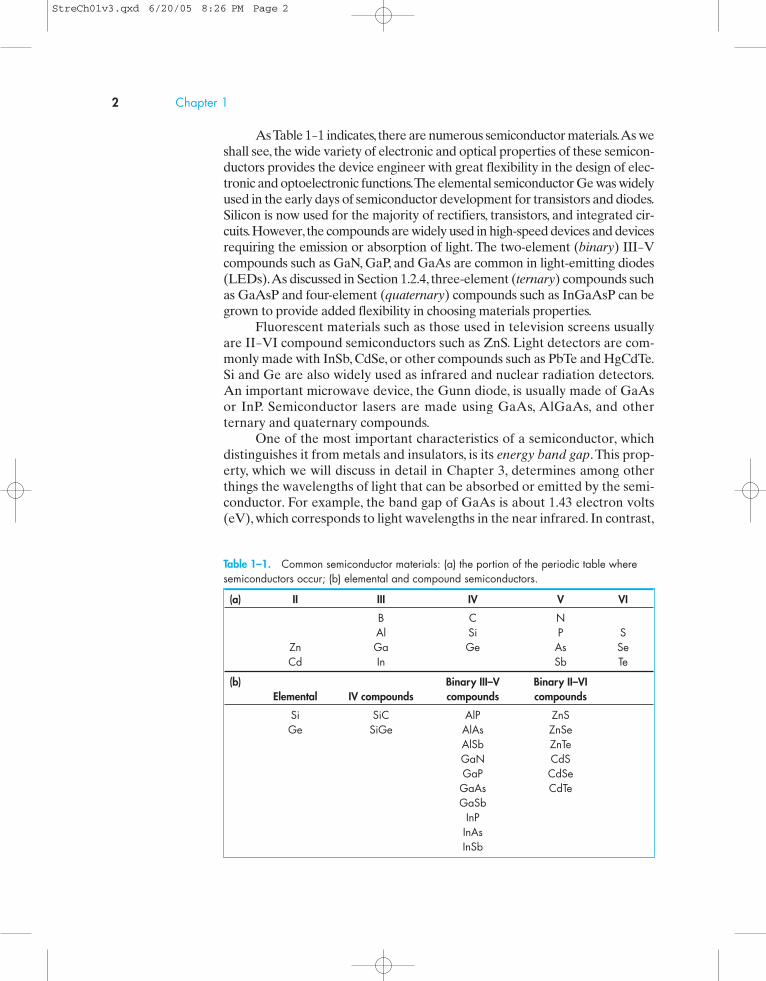
Table 1–1. Common semiconductor materials: (a) the portion of the periodic table wheresemiconductors occur; (b) elemental and compound semiconductors.
(a) II III IV V VI
B C NAl Si P S
Zn Ga Ge As SeCd In Sb Te
(b) Binary III—V Binary II—VIElemental IV compounds compounds compounds
Si SiC AlP ZnSGe SiGe AlAs ZnSe
AlSb ZnTeGaN CdSGaP CdSeGaAs CdTeGaSb
InPInAsInSb
As Table 1—1 indicates, there are numerous semiconductor materials.As weshall see, the wide variety of electronic and optical properties of these semicon-ductors provides the device engineer with great flexibility in the design of elec-tronic and optoelectronic functions.The elemental semiconductor Ge was widelyused in the early days of semiconductor development for transistors and diodes.Silicon is now used for the majority of rectifiers, transistors, and integrated cir-cuits.However, the compounds are widely used in high-speed devices and devicesrequiring the emission or absorption of light. The two-element (binary) III—Vcompounds such as GaN, GaP, and GaAs are common in light-emitting diodes(LEDs).As discussed in Section 1.2.4, three-element (ternary) compounds suchas GaAsP and four-element (quaternary) compounds such as InGaAsP can begrown to provide added flexibility in choosing materials properties.
Fluorescent materials such as those used in television screens usuallyare II—VI compound semiconductors such as ZnS. Light detectors are com-monly made with InSb, CdSe, or other compounds such as PbTe and HgCdTe.Si and Ge are also widely used as infrared and nuclear radiation detectors.An important microwave device, the Gunn diode, is usually made of GaAsor InP. Semiconductor lasers are made using GaAs, AlGaAs, and otherternary and quaternary compounds.
One of the most important characteristics of a semiconductor, whichdistinguishes it from metals and insulators, is its energy band gap.This prop-erty, which we will discuss in detail in Chapter 3, determines among otherthings the wavelengths of light that can be absorbed or emitted by the semi-conductor. For example, the band gap of GaAs is about 1.43 electron volts(eV), which corresponds to light wavelengths in the near infrared. In contrast,
StreCh01v3.qxd 6/20/05 8:26 PM Page 2

GaP has a band gap of about 2.3 eV, corresponding to wavelengths in thegreen portion of the spectrum.1 The band gap Eg for various semiconductormaterials is listed along with other properties in Appendix III.As a result ofthe wide variety of semiconductor band gaps, light-emitting diodes and laserscan be constructed with wavelengths over a broad range of the infrared andvisible portions of the spectrum.
The electronic and optical properties of semiconductor materials arestrongly affected by impurities, which may be added in precisely controlledamounts. Such impurities are used to vary the conductivities of semicon-ductors over wide ranges and even to alter the nature of the conductionprocesses from conduction by negative charge carriers to positive charge car-riers. For example, an impurity concentration of one part per million canchange a sample of Si from a poor conductor to a good conductor of electriccurrent. This process of controlled addition of impurities, called doping, willbe discussed in detail in subsequent chapters.
To investigate these useful properties of semiconductors, it is necessary tounderstand the atomic arrangements in the materials. Obviously, if slight alter-ations in purity of the original material can produce such dramatic changes inelectrical properties, then the nature and specific arrangement of atoms in eachsemiconductor must be of critical importance.Therefore, we begin our study ofsemiconductors with a brief introduction to crystal structure.
In this section we discuss the arrangements of atoms in various solids. Weshall distinguish between single crystals and other forms of materials andthen investigate the periodicity of crystal lattices. Certain important crystal-lographic terms will be defined and illustrated in reference to crystals hav-ing a basic cubic structure. These definitions will allow us to refer to certainplanes and directions within a lattice. Finally, we shall investigate the dia-mond lattice; this structure, with some variations, is typical of most of thesemiconductor materials used in electronic devices.
1.2.1 Periodic Structures
A crystalline solid is distinguished by the fact that the atoms making up thecrystal are arranged in a periodic fashion.That is, there is some basic arrange-ment of atoms that is repeated throughout the entire solid.Thus the crystal ap-pears exactly the same at one point as it does at a series of other equivalentpoints, once the basic periodicity is discovered. However, not all solids arecrystals (Fig. 1—1); some have no periodic structure at all (amorphous solids),and others are composed of many small regions of single-crystal material(polycrystalline solids).The high-resolution micrograph shown in Fig. 6—33 il-lustrates the periodic array of atoms in the single-crystal silicon of a transis-tor channel compared with the amorphous SiO2 (glass) of the oxide layer.
Crystal Properties and Growth of Semiconductors 3
1The conversion between the energy E of a photon of light (eV) and its wavelength �(�m) is � = 1.24/E.For GaAs, � = 1.24/1.43 = 0.87 �m.
1.2CRYSTAL LATTICES
StreCh01v3.qxd 6/20/05 8:26 PM Page 3

4 Chapter 1
(b) Amorphous (c) Polycrystalline(a) Crystalline
Figure 1—1Three types of solids, classified according to atomic arrangement: (a) crystalline and (b) amorphous ma-terials are illustrated by microscopic views of the atoms, whereas (c) polycrystalline structure is illustratedby a more macroscopic view of adjacent single-crystalline regions, such as (a).
r
O a
b
ED
P Q
RS
T
F
O'
E'D'
F'
Figure 1—2A two-dimensional
lattice showingtranslation of a
unit cell by r = 3a + 2b.
The periodicity in a crystal is defined in terms of a symmetric array ofpoints in space called the lattice.We can add atoms at each lattice point in anarrangement called a basis, which can be one atom or a group of atoms hav-ing the same spatial arrangement, to get a crystal. In every case, the latticecontains a volume or cell that represents the entire lattice and is regularly re-peated throughout the crystal.As an example of such a lattice, Fig. 1—2 showsa two-dimensional arrangement of atoms called a rhombic lattice, with aprimitive cell ODEF, which is the smallest such cell. Notice that we can de-fine vectors a and b such that if the primitive cell is translated by integralmultiples of these vectors, a new primitive cell identical to the original isfound (e.g., O�D�E�F�).These vectors, a and b (and c if the lattice is three di-mensional), are called the primitive vectors for the lattice. Points within thelattice are indistinguishable if the vector between the points is
(1—1)
where p, q, and s are integers.A primitive cell has lattice points only at the cor-ners of the cell. It is not unique, but the convention is to choose the smallest
r = pa + qb + sc
StreCh01v3.qxd 6/20/05 8:26 PM Page 4

Crystal Properties and Growth of Semiconductors 5
a
Simple cubic Body-centered cubic Face-centered cubic
a a
Figure 1—3Unit cells for threetypes of cubic lat-tice structures.
primitive vectors. Note that, in a primitive cell, the lattice points at the cornersare shared with adjacent cells; thus, the effective number of lattice points be-longing to the primitive cell is always unity. Since there are many differentways of placing atoms in a volume, the distances and orientation betweenatoms can take many forms, but it is the symmetry that determines the lat-tice, not the magnitudes of the distances between the lattice points.
In many lattices, however, the primitive cell is not the most convenientto work with. For example, in Fig. 1—2, we see that the rhombic arrangementof the lattice points is such that it can also be considered to be rectangular(PQRS) with a lattice point in the center at T (a so-called centered rectangularlattice). [Note that this is not true of all rhombic lattices!] Clearly, it is sim-pler to deal with a rectangle rather than a rhombus. So, in this case we canchoose to work with a larger rectangular unit cell, PQRS, rather than thesmallest primitive cell, ODEF. A unit cell allows lattice points not only at thecorners, but also at the face center (and body center in 3-D) if necessary. Itis sometimes used instead of the primitive cell if it can represent the symmetryof the lattice better (in this example “centered rectangular” 2-D lattice). Itreplicates the lattice by integer translations of basis vectors.
The importance of the unit cell lies in the fact that we can analyze thecrystal as a whole by investigating a representative volume. For example,from the unit cell we can find the distances between nearest atoms and nextnearest atoms for calculation of the forces holding the lattice together; we canlook at the fraction of the unit cell volume filled by atoms and relate thedensity of the solid to the atomic arrangement. But even more important forour interest in electronic devices, the properties of the periodic crystal latticedetermine the allowed energies of electrons that participate in the conduc-tion process.Thus the lattice determines not only the mechanical propertiesof the crystal but also its electrical properties.
1.2.2 Cubic Lattices
The simplest three-dimensional lattice is one in which the unit cell is a cubicvolume, such as the three cells shown in Fig. 1—3. The simple cubic structure(abbreviated sc) has an atom located at each corner of the unit cell.The body-centered cubic (bcc) lattice has an additional atom at the center of the cube,and the face-centered cubic (fcc) unit cell has atoms at the eight corners andcentered on the six faces. All three structures have different primitive cells,but the same cubic unit cell. We will generally work with unit cells.
StreCh01v3.qxd 6/20/05 8:26 PM Page 5

SOLUTION
6 Chapter 1
a /2a /2
a
12
a 2
Figure 1—4Packing of hard
spheres in an fcclattice.
As atoms are packed into the lattice in any of these arrangements, the dis-tances between neighboring atoms will be determined by a balance between theforces that attract them together and other forces that hold them apart.We shalldiscuss the nature of these forces for particular solids in Section 3.1.1. For now,we can calculate the maximum fraction of the lattice volume that can be filledwith atoms by approximating the atoms as hard spheres. For example, Fig. 1—4illustrates the packing of spheres in a face-centered cubic cell of side a, such thatthe nearest neighbors touch. The dimension a for a cubic unit cell is called thelattice constant. For the fcc lattice the nearest neighbor distance is one-half thediagonal of a face, or (a ).Therefore, for the atom centered on the face to�21
2
EXAMPLE 1—1 For a bcc lattice of identical atoms with a lattice constant of 5 Å, calculatethe maximum packing fraction and the radius of the atoms treated as hardspheres with the nearest neighbors touching.
Each corner atom in a cubic unit cell is shared with seven neighbor-ing cells; thus, each unit cell contains one-eighth of a sphere at each of theeight corners for a total of one atom. The bcc cell contains one atom inthe center of the cube. Thus, we have
Å
Volume of each atom =
43
�(2.165)3= 42.5 A° 3
Radius of each atom =
12
* 4.330 A° = 2.165 A°
Nearest atoms are at a separation 12
* 252+ 52
+ 52= 4.330
StreCh01v3.qxd 6/20/05 8:26 PM Page 6

just touch the atoms at each corner of the face, the radius of the sphere must beone-half the nearest neighbor distance, or (a ).
1.2.3 Planes and Directions
In discussing crystals it is very helpful to be able to refer to planes and di-rections within the lattice. The notation system generally adopted uses aset of three integers to describe the position of a plane or the direction ofa vector within the lattice.We first set up an xyz coordinate system with theorigin at any lattice point (it does not matter which one because they areall equivalent!), and the axes are lined up with the edges of the cubic unitcell. The three integers describing a particular plane are found in the fol-lowing way:
1. Find the intercepts of the plane with the crystal axes and expressthese intercepts as integral multiples of the basis vectors (the planecan be moved in and out from the origin, retaining its orientation,until such an integral intercept is discovered on each axis).
2. Take the reciprocals of the three integers found in step 1 and reducethese to the smallest set of integers h, k, and l, which have the samerelationship to each other as the three reciprocals.
3. Label the plane (hkl).
�214
SOLUTION
Crystal Properties and Growth of Semiconductors 7
Therefore, if the atoms in a bcc lattice are packed as densely as possi-ble, with no distance between the outer edges of nearest neighbors, 68%of the volume is filled.This is a relatively high percentage compared withsome other lattice structures (Prob. 1.14).
Packing fraction =
42.5 * 2
(5)3 = 68%
Number of atoms per cube = 1 + 8 *
18
= 2
The plane illustrated in Fig. 1—5 has intercepts at 2a, 4b, and 1c along thethree crystal axes. Taking the reciprocals of these intercepts, we get , ,and 1. These three fractions have the same relationship to each other asthe integers 2, 1, and 4 (obtained by multiplying each fraction by 4).Thusthe plane can be referred to as a (214) plane. The only exception is if theintercept is a fraction of the lattice constant a. In that case, we do not re-duce it to the lowest set of integers. For example, in Fig. 1—3, planes par-allel to the cube faces, but going through the body center atoms in the bcclattice, would be (200) and not (100).S1
14
12
EXAMPLE 1—2
StreCh01v3.qxd 6/20/05 8:26 PM Page 7

8 Chapter 1
The three integers h, k, and l are called the Miller indices; these threenumbers define a set of parallel planes in the lattice. One advantage of tak-ing the reciprocals of the intercepts is avoidance of infinities in the nota-tion. One intercept is infinity for a plane parallel to an axis; however, thereciprocal of such an intercept is taken as zero. If a plane contains one of theaxes, it is parallel to that axis and has a zero reciprocal intercept. If a planepasses through the origin, it can be translated to a parallel position for cal-culation of the Miller indices. If an intercept occurs on the negative branchof an axis, the minus sign is placed above the Miller index for convenience,such as
From a crystallographic point of view, many planes in a lattice are equiv-alent; that is, a plane with given Miller indices can be shifted about in the lat-tice simply by choice of the position and orientation of the unit cell. Theindices of such equivalent planes are enclosed in braces { } instead of paren-theses. For example, in the cubic lattice of Fig. 1—6 all the cube faces are crys-tallographically equivalent in that the unit cell can be rotated in variousdirections and still appear the same. The six equivalent faces are collective-ly designated as {100}.
A direction in a lattice is expressed as a set of three integers with thesame relationship as the components of a vector in that direction.The threevector components are expressed in multiples of the basis vectors, and thethree integers are reduced to their smallest values while retaining the rela-tionship among them. For example, the body diagonal in the cubic lattice(Fig. 1—7a) is composed of the components 1a, 1b, and 1c; therefore, this di-agonal is the [111] direction. (Brackets are used for direction indices.) As inthe case of planes, many directions in a lattice are equivalent, depending onlyon the arbitrary choice of orientation for the axes. Such equivalent directionindices are placed in angular brackets � �. For example, the crystal axes in thecubic lattice [100], [010], and [001] are all equivalent and are called �100� di-rections (Fig. 1—7b).
(hkl).
(214)
z
x
y
c
a
b
Figure 1—5A (214) crystal
plane.
StreCh01v3.qxd 6/20/05 8:26 PM Page 8

Crystal Properties and Growth of Semiconductors 9
[111][001]
[100]
[010]
[110]
a
x
y
z
b
c
0
a
x
y
z
b
c
0
(b)(a)
Figure 1—7Crystal directionsin the cubiclattice.
(100)
(001)
(010) x
0
y
z
(100)
(001)
(010)
x
0y
z
Figure 1—6Equivalence ofthe cube faces({100} planes) byrotation of theunit cell within thecubic lattice.
Two useful relationships in terms of Miller indices describe the distancebetween planes and angles between directions. The distance d between twoadjacent planes labeled (hkl) is given in terms of the lattice constant, a, as
(1–2a)
The angle � between two different Miller index directions is given by
(1–2b)Cos � = h1h2 + k1k2 + l1l2/{(h1 2
+ k1 2
+ l1 2)1/2(h2
2+ k2
2+ l2
2)1/2}
d = a/(h2+ k2
+ l2)1/2
StreCh01v3.qxd 6/20/05 8:26 PM Page 9

Comparing Figs. 1—6 and 1—7, we notice that in cubic lattices a direction[hkl] is perpendicular to the plane (hkl). This is convenient in analyzing lat-tices with cubic unit cells, but it should be remembered that it is not neces-sarily true in noncubic systems.
1.2.4 The Diamond Lattice
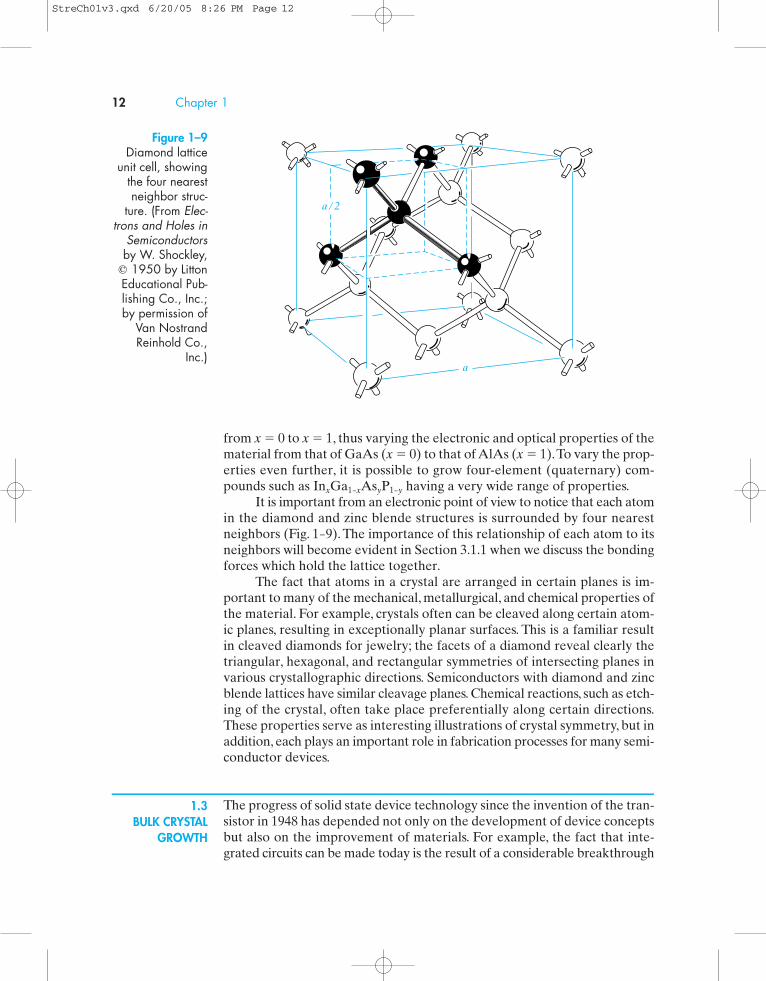
The basic crystal structure for many important semiconductors is the fcc lat-tice with a basis of two atoms, giving rise to the diamond structure, charac-teristic of Si, Ge, and C in the diamond form. In many compoundsemiconductors, atoms are arranged in a basic diamond structure, but aredifferent on alternating sites.This is called a zinc blende structure and is typ-ical of the III–V compounds. One of the simplest ways of stating the con-struction of the diamond structure is the following:
The diamond structure can be thought of as an fcc lattice with anextra atom placed at a/4 � b/4 � c/4 from each of the fcc atoms.
Figure 1—8a illustrates the construction of a diamond lattice from anfcc unit cell. We notice that when the vectors are drawn with componentsone-fourth of the cube edge in each direction, only four additional pointswithin the same unit cell are reached. Vectors drawn from any of the otherfcc atoms simply determine corresponding points in adjacent unit cells. Thismethod of constructing the diamond lattice implies that the original fcc hasassociated with it a second interpenetrating fcc displaced, by , . The twointerpenetrating fcc sublattices can be visualized by looking down on the unitcell of Fig. 1—8a from the top (or along any �100� direction). In the top viewof Fig. 1—8b, atoms belonging to the original fcc are represented by open cir-cles, and the interpenetrating sublattice is shaded. If the atoms are all simi-lar, we call this structure a diamond lattice; if the atoms differ on alternating
14
14
14,
10 Chapter 1
a
a
(a) (b)
Figure 1—8Diamond lattice structure: (a) a unit cell of the diamond lattice constructed by placing atoms , , from each atom in an fcc; (b) top view (along any �100� direction) of an extended diamond lattice. The coloredcircles indicate one fcc sublattice and the black circles indicate the interpenetrating fcc.
14
14
14
StreCh01v3.qxd 6/20/05 8:26 PM Page 10

sites, it is a zinc blende structure. For example, if one fcc sublattice is com-posed of Ga atoms and the interpenetrating sublattice is As, the zinc blendestructure of GaAs results. Most of the compound semiconductors have thistype of lattice, although some of the II—VI compounds are arranged in aslightly different structure called the wurtzite lattice. We shall restrict ourdiscussion here to the diamond and zinc blende structures, since they aretypical of most of the commonly used semiconductors.
SOLUTION
EXAMPLE 1—3Calculate the volume density of Si atoms (number of ), giventhat the lattice constant of Si is 5.43 Å. Calculate the areal density of atoms
on the (100) plane.
On the (100) plane, we have four atoms on corners and one on theface center.
For Si, we have 8 corner lattice points, 6 face centered points, and 2atoms
Volume density =
8
(5.43 * 10- 8)3 = 5.00 * 1022 cm- 3
Number of atoms per cube = ¢8 *
18
+
12
* 6≤ * 2 = 8
(100) plane: 4 *
14
+ 1
(5.43 * 10- 8)(5.43 * 10- 8)= 6.8 * 1014 cm- 2
(number/cm2)
atoms/cm3
Crystal Properties and Growth of Semiconductors 11
A particularly interesting and useful feature of the III—V compoundsis the ability to vary the mixture of elements on each of the two interpene-trating fcc sublattices of the zinc blende crystal. For example, in the ternarycompound AlGaAs, it is possible to vary the composition of the ternary alloyby choosing the fraction of Al or Ga atoms on the column III sublattice. It iscommon to represent the composition by assigning subscripts to the variouselements. For example,AlxGa1—xAs refers to a ternary alloy in which the col-umn III sublattice in the zinc blende structure contains a fraction x of Alatoms and 1—x of Ga atoms.The composition Al0.3Ga0.7As has 30 percent Aland 70 percent Ga on the column III sites, with the interpenetrating columnV sublattice occupied entirely by As atoms. It is extremely useful to be ableto grow ternary alloy crystals such as this with a given composition. For theAlxGa1—xAs example we can grow crystals over the entire composition range
StreCh01v3.qxd 6/20/05 8:26 PM Page 11
from x � 0 to x � 1, thus varying the electronic and optical properties of thematerial from that of GaAs (x � 0) to that of AlAs (x � 1).To vary the prop-erties even further, it is possible to grow four-element (quaternary) com-pounds such as InxGa1—xAsyP1—y having a very wide range of properties.
It is important from an electronic point of view to notice that each atomin the diamond and zinc blende structures is surrounded by four nearestneighbors (Fig. 1—9). The importance of this relationship of each atom to itsneighbors will become evident in Section 3.1.1 when we discuss the bondingforces which hold the lattice together.
The fact that atoms in a crystal are arranged in certain planes is im-portant to many of the mechanical, metallurgical, and chemical properties ofthe material. For example, crystals often can be cleaved along certain atom-ic planes, resulting in exceptionally planar surfaces. This is a familiar resultin cleaved diamonds for jewelry; the facets of a diamond reveal clearly thetriangular, hexagonal, and rectangular symmetries of intersecting planes invarious crystallographic directions. Semiconductors with diamond and zincblende lattices have similar cleavage planes. Chemical reactions, such as etch-ing of the crystal, often take place preferentially along certain directions.These properties serve as interesting illustrations of crystal symmetry, but inaddition, each plays an important role in fabrication processes for many semi-conductor devices.
The progress of solid state device technology since the invention of the tran-sistor in 1948 has depended not only on the development of device conceptsbut also on the improvement of materials. For example, the fact that inte-grated circuits can be made today is the result of a considerable breakthrough
12 Chapter 1
a
a / 2
Figure 1—9Diamond lattice
unit cell, showingthe four nearestneighbor struc-
ture. (From Elec-trons and Holes in
Semiconductorsby W. Shockley,
� 1950 by LittonEducational Pub-lishing Co., Inc.;by permission of
Van NostrandReinhold Co.,
Inc.)
1.3BULK CRYSTAL
GROWTH
StreCh01v3.qxd 6/20/05 8:26 PM Page 12

Crystal Properties and Growth of Semiconductors 13
in the growth of pure, single-crystal Si in the early and mid-1950s. The re-quirements on the growing of device-grade semiconductor crystals are morestringent than those for any other materials. Not only must semiconductorsbe available in large single crystals, but also the purity must be controlledwithin extremely close limits. For example, Si crystals now being used in de-vices are grown with concentrations of most impurities of less than one partin ten billion. Such purities require careful handling and treatment of thematerial at each step of the manufacturing process.
1.3.1 Starting Materials
The raw feedstock for Si crystal is silicon dioxide (SiO2). We react SiO2
with C in the form of coke in an arc furnace at very high temperatures(�1800°C) to reduce SiO2 according to the following reaction:
(1—3)
This forms metallurgical grade Si (MGS) which has impurities such asFe, Al and heavy metals at levels of several hundred to several thousandparts per million (ppm). Refer back to Example 1—3 to see that 1 ppm of Sicorresponds to an impurity level of 5 1016cm3.While MGS is clean enoughfor metallurgical applications such as using Si to make stainless steel, it isnot pure enough for electronic applications; it is also not single crystal.
The MGS is refined further to yield semiconductor-grade or electronic-grade Si (EGS), in which the levels of impurities are reduced to parts per bil-lion or ppb (1 ppb�5 1013cm3). This involves reacting the MGS with dryHCl according to the following reaction to form trichlorosilane, SiHCl3, whichis a liquid with a boiling point of 32°C.
(1—4)
Along with SiHCl3, chlorides of impurities such as FeCl3 are formedwhich fortunately have boiling points that are different from that of SiHCl3.This allows a technique called fractional distillation to be used, in which weheat up the mixture of SiHCl3 and the impurity chlorides, and condense thevapors in different distillation towers held at appropriate temperatures. Wecan thereby separate pure SiHCl3 from the impurities. SiHCl3 is then con-verted to highly pure EGS by reaction with H2,
(1—5)
1.3.2 Growth of Single-Crystal Ingots
Next, we have to convert the high purity but still polycrystalline EGS to single-crystal Si ingots or boules.This is generally done today by a process commonly
2SiHCl3 � 2H2 → 2Si � 6HCl
Si � 3HCl → SiHCl3 � H2
SiO2 � 2C → Si � 2CO
StreCh01v3.qxd 6/20/05 8:26 PM Page 13

14 Chapter 1
Figure 1—10Pulling of a Si crys-
tal from the melt(Czochralski
method): (a) sche-matic diagram ofthe crystal growth
process; (b) an 8-in. diameter,
�100� oriented Sicrystal being
pulled from themelt. (Photograph
courtesy of MEMCElectronics Intl.)
called the Czochralski method. In order to grow single-crystal material, it isnecessary to have a seed crystal which can provide a template for growth. Wemelt the EGS in a quartz-lined graphite crucible by resistively heating it to themelting point of Si (1412°C).
A seed crystal is lowered into the molten material and then is raisedslowly, allowing the crystal to grow onto the seed (Fig. 1—10). Generally, thecrystal is rotated slowly as it grows to provide a slight stirring of the meltand to average out any temperature variations that would cause inhomoge-neous solidification. This technique is widely used in growing Si, Ge, andsome of the compound semiconductors.
In pulling compounds such as GaAs from the melt, it is necessary to pre-vent volatile elements (e.g., As) from vaporizing. In one method a layer ofB2O3, which is dense and viscous when molten, floats on the surface of themolten GaAs to prevent As evaporation.This growth method is called liquid-encapsulated Czochralski (LEC) growth.
In Czochralski crystal growth, the shape of the ingot is determined bya combination of the tendency of the cross section to assume a polygonalshape due to the crystal structure and the influence of surface tension, whichencourages a circular cross section.The crystal facets are noticeable in the ini-tial growth near the seed crystal in Fig. 1—10b. However, the cross section ofthe large ingot in Fig. 1—11 is almost circular.
In the fabrication of Si integrated circuits (Chapter 9) it is economicalto use very large Si wafers, so that many IC chips can be made simultaneously.As a result, considerable research and development have gone into meth-ods for growing very large Si crystals. For example, Fig. 1—11 illustrates a 12-inch-diameter Si ingot, 1.0 m long, weighing 140 kg.
(a)
Pull
Seed
Crucible
GrowingCrystal
Molten Si
(b)
StreCh01v3.qxd 6/20/05 8:26 PM Page 14

Crystal Properties and Growth of Semiconductors 15
Figure 1—11Silicon crystal grown by the Czochralski method. This large single-crystal ingot provides 300 mm (12-in.)diameter wafers when sliced using a saw. The ingot is about 1.0 m long (including the tapered regions),and weighs about 140 kg. (Photograph courtesy of MEMC Electronics Intl.)
1.3.3 Wafers
After the single-crystal ingot is grown, it is then mechanically processed tomanufacture wafers.The first step involves mechanically grinding the more-or-less cylindrical ingot into a perfect cylinder with a precisely controlled di-ameter.This is important because in a modern integrated circuit fabricationfacility many processing tools and wafer handling robots require tight toler-ances on the size of the wafers. Using X-ray crystallography, crystal planes inthe ingot are identified. For reasons discussed in Section 6.4.3, most Si in-gots are grown along the �100� direction (Fig. 1—10). For such ingots, a smallnotch is ground on one side of the cylinder to delineate a {110} face of thecrystal.This is useful because for �100� Si wafers, the {110} cleavage planes areorthogonal to each other. This notch then allows the individual integratedcircuit chips to be made oriented along {110} planes so that when the chipsare sawed apart, there is less chance of spurious cleavage of the crystal, whichcould cause good chips to be lost.
Next, the Si cylinder is sawed into individual wafers about 775 �m thick,by using a diamond-tipped inner-hole blade saw, or a wire saw (Fig. 1—12a).The resulting wafers are mechanically lapped and ground on both sides toachieve a flat surface, and to remove the mechanical damage due to sawing.Such damage would have a detrimental effect on devices.The flatness of thewafer is critical from the point of view of “depth of focus” or how sharp animage can be focussed on the wafer surface during photolithography, as dis-cussed in Chapter 5.The Si wafers are then rounded or “chamfered” along theedges to minimize the likelihood of chipping the wafers during processing.
StreCh01v3.qxd 6/20/05 8:26 PM Page 15

16 Chapter 1
Finally, the wafers undergo chemical-mechanical polishing using a slurry ofvery fine SiO2 particles in a basic NaOH solution to give the front surface ofthe wafer a mirror-like finish.The wafers are now ready for integrated circuitfabrication (Fig. 1—12b). The economic value added in this process is im-pressive. From sand (SiO2) costing pennies, we can obtain Si wafers costinga few hundred dollars, on which we can make hundreds of microprocessors,for example, each costing several hundred dollars.
1.3.4 Doping
As previously mentioned, there are some impurities in the molten EGS.Wemay also add intentional impurities or dopants to the Si melt to change itselectronic properties. At the solidifying interface between the melt and the
Figure 1—12Steps involved inmanufacturing Si
wafers: (a) A300 mm Si cylin-drical ingot, with
a notch on oneside, being
loaded into awire saw to pro-duce Si wafers;(b) a technician
holding a cassetteof 300 mm
wafers. (Photo-graphs courtesy
of MEMC Electronics Intl.)
(a)
(b)
StreCh01v3.qxd 6/20/05 8:26 PM Page 16

solid, there will be a certain distribution of impurities between the two phas-es. An important quantity that identifies this property is the distribution co-efficient kd, which is the ratio of the concentration of the impurity in the solidCS to the concentration in the liquid CL at equilibrium:
(1—6)
The distribution coefficient is a function of the material, the impurity,the temperature of the solid–liquid interface, and the growth rate. For an im-purity with a distribution coefficient of one-half, the relative concentrationof the impurity in the molten liquid to that in the refreezing solid is two toone.Thus the concentration of impurities in that portion of material that so-lidifies first is one-half the original concentration C0. The distribution coef-ficient is thus important during growth from a melt.This can be illustrated byan example involving Czochralski growth:
kd =CS
CL
SOLUTION
Crystal Properties and Growth of Semiconductors 17
EXAMPLE 1—4A Si crystal is to be grown by the Czochralski method, and it is desired thatthe ingot contain 1016 phosphorus atoms/cm3.
(a) What concentration of phosphorus atoms should the melt containto give this impurity concentration in the crystal during the initialgrowth? For P in Si, kd = 0.35.
(b) If the initial load of Si in the crucible is 5 kg,how many grams of phos-phorus should be added? The atomic weight of phosphorus is 31.
(a) Assume that CS = kdCL throughout the growth. Thus the initialconcentration of P in the melt should be
(b) The P concentration is so small that the volume of melt can becalculated from the weight of Si. From Appendix III the density ofSi is 2.33 g/cm3. In this example we will neglect the difference indensity between solid and molten Si.
6.14 1019 atoms 31 g�mole6.02 1023 atoms�mole
= 3.16 103 g of P
2.86 1016 cm3 2146 cm3 = 6.14 1019 P atoms
5000 g of Si2.33 g�cm3 = 2146 cm3 of Si
1016
0.35= 2.86 1016 cm3
StreCh01v3.qxd 6/20/05 8:26 PM Page 17

18 Chapter 1
2The generic term chemical vapor deposition includes the deposition of layers that may be polycrystallineor amorphous. When a CVD process results in a single-crystal epitaxial layer, a more specific term isvapor-phase epitaxy (VPE).
One of the most important and versatile methods of crystal growth for de-vice applications is the growth of a thin crystal layer on a wafer of a com-patible crystal. The substrate crystal may be a wafer of the same material asthe grown layer or a different material with a similar lattice structure. In thisprocess the substrate serves as the seed crystal onto which the new crystallinematerial grows.The growing crystal layer maintains the crystal structure andorientation of the substrate. The technique of growing an oriented single-crystal layer on a substrate wafer is called epitaxial growth, or epitaxy.As weshall see in this section, epitaxial growth can be performed at temperaturesconsiderably below the melting point of the substrate crystal. A variety ofmethods are used to provide the appropriate atoms to the surface of thegrowing layer. These methods include chemical vapor deposition (CVD),2
growth from a melt (liquid-phase epitaxy, LPE), and evaporation of the ele-ments in a vacuum (molecular beam epitaxy, MBE). With this wide range ofepitaxial growth techniques, it is possible to grow a variety of crystals for de-vice applications, having properties specifically designed for the electronic oroptoelectronic device being made.
1.4.1 Lattice-Matching in Epitaxial Growth
When Si epitaxial layers are grown on Si substrates, there is a natural match-ing of the crystal lattice, and high-quality single-crystal layers result. On theother hand, it is often desirable to obtain epitaxial layers that differ somewhatfrom the substrate, which is known as heteroepitaxy. This can be accomplishedeasily if the lattice structure and lattice constant a match for the two mate-rials. For example, GaAs and AlAs both have the zinc blende structure, witha lattice constant of about 5.65 Å. As a result, epitaxial layers of the ternaryalloy AlGaAs can be grown on GaAs substrates with little lattice mismatch.Similarly, GaAs can be grown on Ge substrates (see Appendix III).
Since the P concentration in the growing crystal is only about one-third of that in the melt, Si is used up more rapidly than P in the growth.Thus the melt becomes richer in P as the growth proceeds, and the crys-tal is doped more heavily in the latter stages of growth.This assumes thatkd is not varied; a more uniformly doped ingot can be grown by varyingthe pull rate (and therefore kd) appropriately. Modern Czochralski growthsystems use computer controls to vary the temperature, pull rate, andother parameters to achieve fairly uniformly doped ingots.
1.4EPITAXIALGROWTH
StreCh01v3.qxd 6/20/05 8:26 PM Page 18
Crystal Properties and Growth of Semiconductors 19
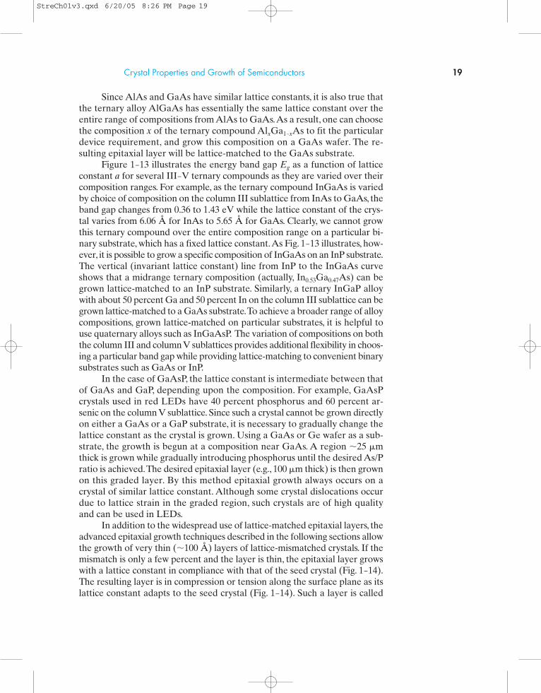
Since AlAs and GaAs have similar lattice constants, it is also true thatthe ternary alloy AlGaAs has essentially the same lattice constant over theentire range of compositions from AlAs to GaAs.As a result, one can choosethe composition x of the ternary compound AlxGa1—xAs to fit the particulardevice requirement, and grow this composition on a GaAs wafer. The re-sulting epitaxial layer will be lattice-matched to the GaAs substrate.
Figure 1—13 illustrates the energy band gap Eg as a function of latticeconstant a for several III—V ternary compounds as they are varied over theircomposition ranges. For example, as the ternary compound InGaAs is variedby choice of composition on the column III sublattice from InAs to GaAs, theband gap changes from 0.36 to 1.43 eV while the lattice constant of the crys-tal varies from 6.06 Å for InAs to 5.65 Å for GaAs. Clearly, we cannot growthis ternary compound over the entire composition range on a particular bi-nary substrate, which has a fixed lattice constant.As Fig. 1—13 illustrates, how-ever, it is possible to grow a specific composition of InGaAs on an InP substrate.The vertical (invariant lattice constant) line from InP to the InGaAs curveshows that a midrange ternary composition (actually, In0.53Ga0.47As) can begrown lattice-matched to an InP substrate. Similarly, a ternary InGaP alloywith about 50 percent Ga and 50 percent In on the column III sublattice can begrown lattice-matched to a GaAs substrate.To achieve a broader range of alloycompositions, grown lattice-matched on particular substrates, it is helpful touse quaternary alloys such as InGaAsP. The variation of compositions on boththe column III and column V sublattices provides additional flexibility in choos-ing a particular band gap while providing lattice-matching to convenient binarysubstrates such as GaAs or InP.
In the case of GaAsP, the lattice constant is intermediate between thatof GaAs and GaP, depending upon the composition. For example, GaAsPcrystals used in red LEDs have 40 percent phosphorus and 60 percent ar-senic on the column V sublattice. Since such a crystal cannot be grown directlyon either a GaAs or a GaP substrate, it is necessary to gradually change thelattice constant as the crystal is grown. Using a GaAs or Ge wafer as a sub-strate, the growth is begun at a composition near GaAs. A region �25 �mthick is grown while gradually introducing phosphorus until the desired As/Pratio is achieved.The desired epitaxial layer (e.g., 100 �m thick) is then grownon this graded layer. By this method epitaxial growth always occurs on acrystal of similar lattice constant. Although some crystal dislocations occurdue to lattice strain in the graded region, such crystals are of high qualityand can be used in LEDs.
In addition to the widespread use of lattice-matched epitaxial layers, theadvanced epitaxial growth techniques described in the following sections allowthe growth of very thin (�100 Å) layers of lattice-mismatched crystals. If themismatch is only a few percent and the layer is thin, the epitaxial layer growswith a lattice constant in compliance with that of the seed crystal (Fig. 1—14).The resulting layer is in compression or tension along the surface plane as itslattice constant adapts to the seed crystal (Fig. 1—14). Such a layer is called
StreCh01v3.qxd 6/20/05 8:26 PM Page 19

20 Chapter 1
pseudomorphic because it is not lattice-matched to the substrate without strain.However, if the epitaxial layer exceeds a critical layer thickness, tc, which de-pends on the lattice mismatch, the strain energy leads to formation of defectscalled misfit dislocations. Using thin alternating layers of slightly mismatchedcrystal layers, it is possible to grow a strained-layer superlattice (SLS) in whichalternate layers are in tension and compression. The overall SLS lattice con-stant is an average of that of the two bulk materials.
0.496
0.620
0.827
1.241.3
1.55
2.48
Wav
elen
gth
(�m
)at
the
band
gap
ene
rgy
GaAs InP
Binary substrates
5.4
2.5
2.0
1.5
1.0
0.5
Ban
d G
ap (
eV)
5.6 5.8 6.0 6.2
Lattice constant (Å)
x � 0.2
0.4
0.6
0.8
AlSb
GaSb
GaP
InAs
GaAs InP
AlAs
In x Ga1-xAs
Figure 1—13Relationship between band gap and lattice constant for alloys in the InGaAsP and AlGaAsSb systems.The dashed vertical lines show the lattice constants for the commercially available binary substratesGaAs and InP. For the marked example of InxGa1—xAs, the ternary composition x � 0.53 can be grownlattice-matched on InP, since the lattice constants are the same. For quaternary alloys, the compositionson both the III and V sublattices can be varied to grow lattice-matched epitaxial layers along the dashedvertical lines between curves. For example, InxGa1—xAsyP1—y can be grown on InP substrates, with result-ing band gaps ranging from 0.75 eV to 1.35 eV. In using this figure, assume the lattice constant a of aternary alloy varies linearly with the composition x.
StreCh01v3.qxd 6/20/05 8:26 PM Page 20

Crystal Properties and Growth of Semiconductors 21
SiGe
Si
t � tc t � tc(b)(a)
Figure 1—14Heteroepitaxy and misfit dislocations. For example, in heteroepitaxy of a SiGe layer on Si, the latticemismatch between SiGe and Si leads to compressive strain in the SiGe layer. The amount of strain de-pends on the mole fraction of Ge. (a) For layer thicknesses less than the critical layer thickness, tc,pseudomorphic growth occurs. (b) However, above tc, misfit dislocations form at the interface which mayreduce the usefulness of the layers in device applications.
1.4.2 Vapor-Phase Epitaxy
The advantages of low temperature and high purity epitaxial growth canbe achieved by crystallization from the vapor phase. Crystalline layers canbe grown onto a seed or substrate from a chemical vapor of the semicon-ductor material or from mixtures of chemical vapors containing the semi-conductor. Vapor-phase epitaxy (VPE) is a particularly important sourceof semiconductor material for use in devices. Some compounds such asGaAs can be grown with better purity and crystal perfection by vapor epi-taxy than by other methods. Furthermore, these techniques offer greatflexibility in the actual fabrication of devices. When an epitaxial layer isgrown on a substrate, it is relatively simple to obtain a sharp demarcationbetween the type of impurity doping in the substrate and in the grownlayer. The advantages of this freedom to vary the impurity will be dis-cussed in subsequent chapters. We point out here, however, that Si inte-grated-circuit devices (Chapter 9) are usually built in layers grown by VPEon Si wafers.
StreCh01v3.qxd 6/20/05 8:26 PM Page 21

22 Chapter 1
Radio frequencysource
Gas inlet
Vent
Quartz chamber
Gas baffle
Susceptor
Pedestal
Wafers
Figure 1—15A barrel-type re-actor for Si VPE.These are atmos-
pheric pressuresystems. The Si
wafers are held inslots cut on thesides of a SiC-
coated graphitesusceptor that
flares out near thebase to promote
gas flow patternsconducive to uni-
form epitaxy.
Epitaxial layers are generally grown on Si substrates by the controlleddeposition of Si atoms onto the surface from a chemical vapor containingSi. In one method, a gas of silicon tetrachloride reacts with hydrogen gas togive Si and anhydrous HCl:
(1—7)
If this reaction occurs at the surface of a heated crystal, the Si atoms re-leased in the reaction can be deposited as an epitaxial layer.The HCl remainsgaseous at the reaction temperature and does not disturb the growing crys-tal. As indicated, this reaction is reversible. This is very important because itimplies that by adjusting the process parameters, the reaction in Eq. (1—7) canbe driven to the left (providing etching of the Si rather than deposition).Thisetching can be used for preparing an atomically clean surface on which epi-taxy can occur.
This vapor epitaxy technique requires a chamber into which the gases canbe introduced and a method for heating the Si wafers. Since the chemical re-actions take place in this chamber, it is called a reaction chamber or, more sim-ply, a reactor. Hydrogen gas is passed through a heated vessel in which SiCl4
is evaporated; then the two gases are introduced into the reactor over the sub-strate crystal, along with other gases containing the desired doping impurities.The Si slice is placed on a graphite susceptor or some other material that canbe heated to the reaction temperature with an rf heating coil or tungsten halo-gen lamps.This method can be adapted to grow epitaxial layers of closely con-trolled impurity concentration on many Si slices simultaneously (Fig. 1—15).
The reaction temperature for the hydrogen reduction of SiCl4 is approx-imately 1150—1250°C. Other reactions may be employed at somewhat lowertemperatures, including the use of dichlorosilane (SiH2Cl2) at 1000—1100°C, or
SiCl4 � 2H2⇀↽ Si � 4HCl
StreCh01v3.qxd 6/20/05 8:26 PM Page 22

Crystal Properties and Growth of Semiconductors 23
the pyrolysis of silane (SiH4) at 500°C–1000°C. Pyrolysis involves the breakingup of the silane at the reaction temperature:
(1—8)
There are several advantages of the lower reaction temperatureprocesses, including the fact that they reduce migration of impurities from thesubstrate to the growing epitaxial layer.
In some applications it is useful to grow thin Si layers on insulating sub-strates. For example, vapor-phase epitaxial techniques can be used to grow�1�m Si films on sapphire and other insulators. This application of VPE isdiscussed in Section 9.3.2.
Vapor-phase epitaxial growth is also important in the III—V com-pounds, such as GaAs, GaP, and the ternary alloy GaAsP, which is widelyused in the fabrication of LEDs. Substrates are held at about 800°C on a ro-tating wafer holder while phosphine, arsine, and gallium chloride gases aremixed and passed over the samples.The GaCl is obtained by reacting anhy-drous HCl with molten Ga within the reactor. Variation of the crystal com-position for GaAsP can be controlled by altering the mixture of arsine andphosphine gases.
Another useful method for epitaxial growth of compound semiconduc-tors is called metal-organic vapor-phase epitaxy (MOVPE), or organometal-lic vapor-phase epitaxy (OMVPE). For example, the organometallic compoundtrimethylgallium can be reacted with arsine to form GaAs and methane:
(1—9)
This reaction takes place at about 700°C, and epitaxial growth of high-quality GaAs layers can be obtained. Other compound semiconductors canalso be grown by this method. For example, trimethylaluminum can be addedto the gas mixture to grow AlGaAs.This growth method is widely used in thefabrication of a variety of devices, including solar cells and lasers. The con-venient variability of the gas mixture allows the growth of multiple thin lay-ers similar to those discussed below for molecular beam epitaxy.
1.4.3 Molecular Beam Epitaxy
One of the most versatile techniques for growing epitaxial layers is calledmolecular beam epitaxy (MBE). In this method the substrate is held in a highvacuum while molecular or atomic beams of the constituents impinge uponits surface (Fig. 1—16a). For example, in the growth of AlGaAs layers on GaAssubstrates, the Al, Ga, and As components, along with dopants, are heated inseparate cylindrical cells. Collimated beams of these constituents escape intothe vacuum and are directed onto the surface of the substrate. The rates atwhich these atomic beams strike the surface can be closely controlled, andgrowth of very high quality crystals results. The sample is held at a relative-ly low temperature (about 600°C for GaAs) in this growth procedure.Abrupt
(CH3)3Ga � AsH3 → GaAs � 3CH4
SiH4 → Si � 2H2
StreCh01v3.qxd 6/20/05 8:26 PM Page 23

24 Chapter 1
(a)
Substrate
GaAs
Molecular beams
Sources
Be
AsGaAl
Si
Shutters
Figure 1—16Crystal growth by molecular beam epitaxy (MBE): (a) evaporation cells inside a high-vacuum chamberdirecting beams of Al, Ga, As, and dopants onto a GaAs substrate; (b) scanning electron micrograph of the cross section of an MBE-grown crystal having alternating layers of GaAs (dark lines) and AlGaAs (light lines). Each layer is four monolayers (4 a/2 � 11.3 Å) thick. (Photograph courtesy of Bell Laboratories.)
(a)
(b)
StreCh01v3.qxd 6/20/05 8:26 PM Page 24

Figure 1—17Molecular beamepitaxy facility inthe Microelectron-ics Research Cen-ter at theUniversity ofTexas at Austin.
Crystal Properties and Growth of Semiconductors 25
changes in doping or in crystal composition (e.g., changing from GaAs to Al-GaAs) can be obtained by controlling shutters in front of the individualbeams. Using slow growth rates (� 1 �m/h), it is possible to control the shut-ters to make composition changes on the scale of the lattice constant. Forexample, Fig. 1—16b illustrates a portion of a crystal grown with alternatinglayers of GaAs and AlGaAs only four monolayers thick. Because of the highvacuum and close controls involved, MBE requires a rather sophisticatedsetup (Fig. 1—17). However, the versatility of this growth method makes itvery attractive for many applications.
As MBE has developed in recent years, it has become common to re-place some of the solid sources shown in Fig. 1—16 with gaseous chemicalsources. This approach, called chemical beam epitaxy, or gas-source MBE,combines many of the advantages of MBE and VPE.
1.1 Semiconductor devices are at the heart of information technology. Elementalsemiconductors such as Si appear in column IV of the periodic table, whilecompound semiconductors such as GaAs consist of elements symmetricallyaround column IV. More complicated alloy semiconductors are used to optimizeoptoelectronic properties.
1.2 These devices are generally made in single-crystal material for best perfor-mance. Single crystals have long-range order, while polycrystalline and amor-phous materials have short-range and no order, respectively.
1.3 Lattices are determined by symmetry. In 3-D, these are called Bravais lattices.When we put a basis of atom(s) on the lattice sites, we get a crystal. Common
SUMMARY
StreCh01v3.qxd 6/20/05 8:26 PM Page 25

26 Chapter 1
semiconductors have an fcc symmetry with a basis of two identical or differentatoms, resulting in diamond or zinc blende crystals, respectively.
1.4 The fundamental building block of a lattice is a primitive cell with lattice points atits corners. Sometimes it is easier to describe the crystal in terms of a larger “unit”cell with lattice points not only at the corners, but also at body or face centers.
1.5 Translating unit cells by integer numbers of basis vectors can replicate the lat-tice. Planes and directions in a lattice can be defined in terms of Miller indices.
1.6 Real crystals can have defects in 0-, 1-, 2-, and 3-D, some of which are benign,but many of which are harmful for device operation.
1.7 Semiconductor bulk crystals are grown from a melt by the Czochralski method,starting from a seed. Single-crystal epitaxial layers can be grown on top of semi-conductor wafers in various ways, such as vapor-phase epitaxy, MOCVD, orMBE. One can thereby optimize doping and band-structure properties for de-vice fabrication.
1.1 Using Appendix III, which of the listed semiconductors in Table 1—1 has thelargest band gap? The smallest? What are the corresponding wavelengths iflight is emitted at the energy Eg? Is there a noticeable pattern in the band gapenergy of III–V compounds related to the column III element?
1.2 Find the fraction of the fcc unit cell volume filled with hard spheres.
1.3 Label the planes illustrated in Fig. P1—3.
PROBLEMS
(a) (b)
a
x
z
y
b
ca
x
z
y
b
c
Figure P1—3
1.4 Calculate the densities of Si and GaAs from the lattice constants (AppendixIII), atomic weights, and Avogadro’s number. Compare the results with densi-ties given in Appendix III. The atomic weights of Si, Ga, and As are 28.1, 69.7,and 74.9, respectively.
1.5 The atomic radii of In and Sb atoms are approximately 1.44 Å and 1.36 Å, re-spectively. Using the hard-sphere approximation, find the lattice constant ofInSb (zinc blende structure), and the volume of the primitive cell. What is theatomic density on the (110) planes? (Hint: The volume of the primitive cell isone-fourth the fcc unit cell volume.)
StreCh01v3.qxd 6/20/05 8:26 PM Page 26

1.6 A crystal with a simple cubic lattice and a monoatomic basis has an atomic ra-dius of 2.5 Å and an atomic weight of 5.42. Calculate its density, assuming thatthe atoms touch each other.
1.7 Sketch a view down a �110� direction of a diamond lattice, using Fig. 1—9 as aguide. Include lines connecting nearest neighbors.
1.8 Show by a sketch that the bcc lattice can be represented by two interpenetrat-ing sc lattices. To simplify the sketch, show a �100� view of the lattice.
1.9 (a) Find the number of atoms/cm2 on the (100) surface of a Si wafer.
(b) What is the distance (in Å) between nearest In neighbors in InP?
1.10 The ionic radii of Na+ (atomic weight 23) and Cl (atomic weight 35.5) are 1.0and 1.8 Å, respectively.Treating the ions as hard spheres, calculate the densityof NaCl. Compare this with the measured density of 2.17 g/cm3.
1.11 Sketch an sc unit cell with lattice constant a = 4 Å, whose diatomic basis ofatom A is located at the lattice sites, and with atom B displaced by (a/2,0,0).As-sume that both atoms have the same size and we have a close-packed structure(i.e., nearest neighbor atoms touch each other). Calculate
(i) the packing fraction (i.e., fraction of the total volume occupied by atoms),
(ii) the number of B atoms per unit volume,
(iii) the number of A atoms per unit area on (100) planes.
1.12 How many atoms are found inside a unit cell of an sc, a bcc, and an fcc crystal?How far apart in terms of lattice constant a are the nearest neighbor atoms in eachcase, measured from center to center?
1.13 Draw a cube such as Fig. 1—7, and show four {111} planes with different orien-tations. Repeat for {110} planes.
1.14 Find the maximum fractions of the unit cell volume that can be filled by hardspheres in the sc, fcc, and diamond lattices.
1.15 Calculate the densities of Ge and InP from the lattice constants (AppendixIII), atomic weights, and Avogadro’s number. Compare the results with thedensities given in Appendix III.
1.16 Beginning with a sketch of an fcc lattice, add atoms at from each fccatom to obtain the diamond lattice. Show that only the four added atoms inFig. 1—8a appear in the diamond unit cell.
1.17 Assuming that the lattice constant varies linearly with composition x for aternary alloy (e.g., see the variation for InGaAs in Fig. 1—13), what compositionof AlSbxAs1–x is lattice-matched to InP? What composition of InxGa1–xP is lat-tice-matched to GaAs? What is the band gap energy in each case?
(Note: Such linear variations of crystal properties (e.g., lattice constant andband gap) with mole fraction in alloys is known as Vegard’s law. A second-order polynomial or quadratic fit to the data is called the bowing parameter.)
1.18 An Si crystal is to be pulled from the melt and doped with arsenic (kd = 0.3).If the Si weighs 1 kg, how many grams of arsenic should be introduced toachieve 1015 cm3 doping during the initial growth?
(14,
14,
14)
Crystal Properties and Growth of Semiconductors 27
StreCh01v3.qxd 6/20/05 8:26 PM Page 27

Ashcroft, N. W., and N. D. Mermin. Solid State Physics. Philadelphia: W.B. Saunders,1976.
Denbaars, S. P. “Gallium–Nitride-Based Materials for Blue to Ultraviolet Optoelec-tronic Devices,” Proc. IEEE 85(11) (November 1997): 1740–1749.
Kittel, C. Introduction to Solid State Physics, 7th ed. New York: Wiley, 1996.Plummer, J. D., M. D. Deal, and P. B. Griffin, Silicon VLSI Technology. Upper Sad-
dle River, NJ: Prentice Hall, 2000.Stringfellow, G. B. Organometallic Vapor-Phase Epitaxy. New York:Academic Press,
1989.Swaminathan, V., and A. T. Macrander. Material Aspects of GaAs and InP Based
Structures. Englewood Cliffs, NJ: Prentice Hall, 1991.
Question 1
(a) Label the following planes using the correct notation for a cubic lattice of unitcell edge length a (shown within the unit cell).
28 Chapter 1
SELF QUIZ
READING LIST
z
y
a
a
a
x
z
y
a
a
a
x
z
y
a
a
a
x
(b) Write out all of the equivalent directions using the correct notation.
(c) On the two following sets of axes, (1) sketch the [011] direction and (2) a (111)plane (for a cubic system with primitive vectors a, b, and c).
81009
z
y
b
c
a
x
(1)
z
y
b
c
a
x
(2)
StreCh01v3.qxd 6/20/05 8:26 PM Page 28

Question 2
(a) Which of the following three unit cells are primitive cells for the two-dimensionallattice? Circle the correct combination in bold below.
1 / 2 / 3 / 1 and 2 / 1 and 3 / 2 and 3 / 1, 2, and 3
Crystal Properties and Growth of Semiconductors 29
(b) The following planes (shown within the first quadrant for 0 < x,y,z < a only, withthe dotted lines for reference only) are all from what one set of equivalentplanes? Use correct notation:
answer:
unit cell 2
unit cell 1
unit cell 3
z
y
a
a
a
x
z
y
a
a
a
x
z
y
a
a
a
x
(c) Which of the following three planes (shown within the first quadrant only) is a(121) plane? Circle the correct diagram.
z
ya 2a
a
a
x
z
y
aa/2
a
a
x
z
y
a
a
a
x
StreCh01v3.qxd 6/20/05 8:26 PM Page 29

Question 3
(a) Diamond and zinc blende crystal structures are both composed of a Bravais lat-tice with a two-atom basis. Circle the correct unit cell for this Bravais lattice.
30 Chapter 1
(b) Which statement below is true?
1. GaAs has a diamond / zinc blende crystal structure.
2. Si has a diamond / zinc blende crystal structure.
Question 4
Give some examples of zero-dimensional,one-dimensional, two-dimensional, and three-dimensional defects in a semiconductor.
Question 5
(a) What is the difference between a primitive cell and a unit cell? What is the util-ity of both concepts?
(b) What is the difference between a lattice and a crystal? How many different 1-Dlattices can you have?
Question 6
Consider growing InAs on the following crystal substrates: InP,AlAs, GaAs, and GaP.For which case would the critical thickness of the InAs layer be greatest? You may useFig. 1—13 from your text.
GaP / GaAs / AlAs / InP
StreCh01v3.qxd 6/20/05 8:26 PM Page 30