chapter 25iapc-obp.com/assets/files/302669_09_nmrm_25.pdf · chapter 25 25.2. piezoelectric pvdf...
TRANSCRIPT

Chapter
25
ACOUSTIC WAVE RESONATORS FOR BIOMEDICAL APPLICATIONS
Martín Zalazar*
Faculty of Engineering, National University of Entre Ríos, Argentina. Electronics Prototyping & 3D Research Lab *E-mail: [email protected]
Chapter 25
Contents 25.1. AN ELECTROACTIVE SOLUTION .................................................................................................... 627
25.2. PIEZOELECTRIC PVDF ........................................................................................................................ 628 25.2.1. Numerical model for the PVDF polymer ....................................................................... 628
25.2.1.1. FEM model ................................................................................................................ 629 25.2.2. Resonator fabrication ............................................................................................................ 630 25.2.3. System characterisation ....................................................................................................... 631
25.2.3.1. Cu electrode vs Ag electrode ............................................................................. 632 25.2.4. Influence of PVDF microstructures on cell morphology ........................................ 632 25.2.5. More applications... ................................................................................................................. 633
25.3. BIOCOMPATIBLE ALN MEMBRANE .............................................................................................. 634 25.3.1. Deposition process ................................................................................................................. 635 25.3.2. Characterisation ....................................................................................................................... 636
25.4. AlN AND UNCD... A PROMISE ........................................................................................................... 639 25.4.1. Geometry design ...................................................................................................................... 640 25.4.2. Membrane fabrication ........................................................................................................... 642 25.4.3. Device characterisation ........................................................................................................ 643
25.4.3.1. X-ray diffraction (XRD) ....................................................................................... 643 25.4.3.2. Scanning Electron Microscope (SEM) ........................................................... 643
25.5. COMPARISON TABLE ........................................................................................................................... 645
REFERENCES ...................................................................................................................................................... 646
626
25.1. AN ELECTROACTIVE SOLUTION Materials used as scaffolds for tissue engineering applications are designed to match the structural, morphological, mechanical, and chemical properties of the tissue or organ that will be replaced. Human cells in human tissues are anchorage dependent, the microstructure and surface properties of the scaffolds therefore being a critical issue. In this way, the behaviour of cells cultured on substrates is highly dependent on these characteristics. Surfaces can influence cell behaviour in different aspects such as the growth, adhesion, or morphology of cells. Beyond this, an electrically charged base for tissue engineering applications can be an interesting and promising approach. This fact is particularly important as many body tissues are subjected to varying electro-mechanical solicitation. Conductive materials have thus been used for tissue engineering applications, but some drawbacks exist concerning these materials, such as the need for an external power source to promote electrical stimuli in the cells. Piezoelectric materials are materials that generate varying surface charges under mechanical solicitation and that do not require additional energy sources or electrodes for the generation of the electrical signal [1]. These materials are thus suitable for active tissue engineering strategies in which electroactive response and scaffold microstructure play an essential role. Therefore, the piezoelectric polymer poly(vinylidene fluoride) (PVDF) has attracted interest for its biomedical applications in the fabrication of sensors and actuators and supports for cell cultures. Similarly, aluminium nitride (AlN) has become a very attractive biocompatible piezoelectric material as it is also compatible with complementary metal–oxide–semiconductor (CMOS) technology. This chapter deals with the design and development of piezoelectric biocompatible materials for potential use in tissue engineering applications as a piezoelectric-based scaffold; further, the latest advances in these developments are shown.
627
Chapter 25
25.2. PIEZOELECTRIC PVDF Piezoelectric polymers are a good option for developing piezoelectric-based acoustic wave devices and sensors as well as actuators. In particular, PVDF shows good biocompatibility, chemical resistance, and, in particular, excellent electroactive properties such as piezo-, pyro-, and ferroelectricity. PVDF and its copolymers are the polymers with the highest piezoelectric effect. It has a high dynamic range and wideband and belongs to a new class of piezoelectric plastics characterised by a relatively low dielectric constant, moderate piezoelectric coupling, low acoustic velocities, and low density. One of the mayor advantages of these piezoelectric films is their low acoustic impedance close to water, human tissue, and other organic materials, allowing for a more efficient transduction of acoustic signals due to close impedance matching; this makes them suitable for biological applications. PVDF has three main actuation/sensing modes depending of the fabrication process: inplane mode, thickness mode, and thickness shear mode [2]. A PVDF film under an electric field with a controlled temperature after a mechanical stretch shows very strong piezoelectric and pyroelectric properties. Thin piezoelectric films can also be obtained using soft lithographic techniques by casting and poling, allowing compatibility with microelectromechanical systems (MEMS) technology [3]. PVDF can be made piezoelectric because fluorine is much more electronegative than carbon. The fluorine atoms will attract electrons from the carbon atoms to which they are attached. The −CF2− groups in the chain will be very polar, so when they are placed in an electrical field they will align. Conversely, when the piezopolymer deforms, a macroscopic dipole appears. This can be obtained by submitting the film of polymer to a sufficiently high electric field after mechanical stretching. The obtained polarisation is mainly due to the spatial rearrangement of the polar segments of the macromolecular chains. By machining the material in one or two perpendicular directions prior to the polarisation process, different piezoelectric behaviours can be obtained. This section deals with the design, fabrication, and characterisation of a piezoelectric PVDF for potential use in tissue engineering applications.
25.2.1. Numerical model for the PVDF polymer Previously, the importance of applying electrical signals to body tissues by using piezoelectric materials has been demonstrated. In addition, there are studies showing the feasibility of carrying electrical/mechanical signals on demand by applying an appropriate (wireless) stimuli in order to deform the piezoelectric scaffold microstructure [4,5]. In this sense, the resonance frequency of the piezoelectric implant has to be well known in order to apply the correct excitation.
628

Acoustic wave resonators for biomedical applications
The basic principle of operation for a generic acoustic-wave resonator is a travelling wave combined with a confinement structure to produce a standing wave whose frequency is determined jointly by the velocity of the travelling wave and the dimensions of the confinement structure. A complete model for acoustic systems can be built using the three-port one-dimensional multilayer Mason model [6]. In order to get a more realistic model as a reference, the finite element method (FEM) model fits very well. FEM is a flexible method capable of modelling complicated device geometries, nonuniform material properties, and quite general boundary conditions. PVDF has an orthorhombic symmetry (mm2 class) and is usually operated in thickness mode when the frequency of operation is more than 500 kHz. It has three main actuation/sensing modes depending on the fabrication process: inplane mode (d31, d32), thickness mode (d33), and shear mode (d15, d24).
25.2.1.1. FEM model For a proposed prototype, a disc-shaped PVDF polymer, a three-dimensional (3D) piezoelectric elastic linear solid can be used; the electric potential is applied on both principal surfaces of the disc to avoid electrode modelling. This simplifies the model and reduces simulation times without losing accuracy. The piezoelectric polymer is in thickness excitation mode where the electric field is in the direction of acoustic wave propagation. The elastic matrix c, the piezoelectric coupling matrix e, and the dielectric coefficients matrix at constant strain ε are expressed as follows:
Pa
11 12 13
12 22 23
13 23 33
44
55
66
c c c 0 0 0c c c 0 0 0c c c 0 0 00 0 0 c 0 00 0 0 0 c 00 0 0 0 0 c
=
c
2
Cm
15
24
31 32 33
0 0 0 0 e 00 0 0 e 0 0
e e e 0 0 0
=
e
0 00 00 0
11
22
33
ε =
εε
ε
629
Chapter 25
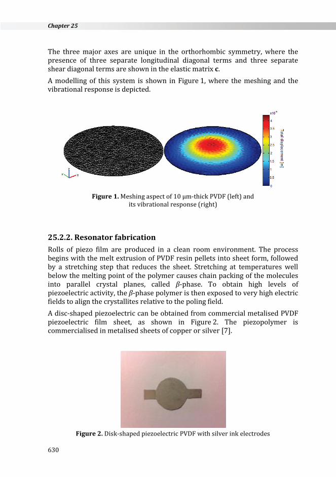
The three major axes are unique in the orthorhombic symmetry, where the presence of three separate longitudinal diagonal terms and three separate shear diagonal terms are shown in the elastic matrix c. A modelling of this system is shown in Figure 1, where the meshing and the vibrational response is depicted.
Figure 1. Meshing aspect of 10 μm-thick PVDF (left) and
its vibrational response (right)
25.2.2. Resonator fabrication Rolls of piezo film are produced in a clean room environment. The process begins with the melt extrusion of PVDF resin pellets into sheet form, followed by a stretching step that reduces the sheet. Stretching at temperatures well below the melting point of the polymer causes chain packing of the molecules into parallel crystal planes, called β-phase. To obtain high levels of piezoelectric activity, the β-phase polymer is then exposed to very high electric fields to align the crystallites relative to the poling field. A disc-shaped piezoelectric can be obtained from commercial metalised PVDF piezoelectric film sheet, as shown in Figure 2. The piezopolymer is commercialised in metalised sheets of copper or silver [7].
Figure 2. Disk-shaped piezoelectric PVDF with silver ink electrodes
630
Acoustic wave resonators for biomedical applications
The circular disk has a diameter of 20 mm and a thickness of 110 μm. Silver ink printed electrodes and copper electrodes patterned with standard lithography on both sides of the disk were used. Printed inks have low sheet resistivity, high current density capability, and are robust mechanically. The overlap between the top and bottom electrode defines an active circular area where the electrical signal for impedance measurements is applied through metal patterned PVDF arms.
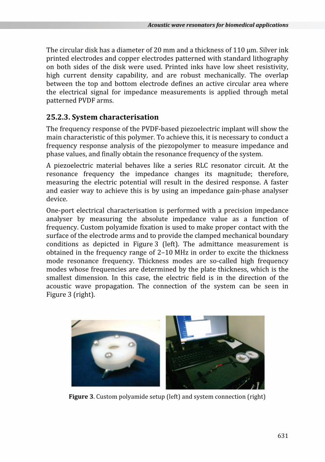
25.2.3. System characterisation The frequency response of the PVDF-based piezoelectric implant will show the main characteristic of this polymer. To achieve this, it is necessary to conduct a frequency response analysis of the piezopolymer to measure impedance and phase values, and finally obtain the resonance frequency of the system. A piezoelectric material behaves like a series RLC resonator circuit. At the resonance frequency the impedance changes its magnitude; therefore, measuring the electric potential will result in the desired response. A faster and easier way to achieve this is by using an impedance gain-phase analyser device. One-port electrical characterisation is performed with a precision impedance analyser by measuring the absolute impedance value as a function of frequency. Custom polyamide fixation is used to make proper contact with the surface of the electrode arms and to provide the clamped mechanical boundary conditions as depicted in Figure 3 (left). The admittance measurement is obtained in the frequency range of 2–10 MHz in order to excite the thickness mode resonance frequency. Thickness modes are so-called high frequency modes whose frequencies are determined by the plate thickness, which is the smallest dimension. In this case, the electric field is in the direction of the acoustic wave propagation. The connection of the system can be seen in Figure 3 (right).
Figure 3. Custom polyamide setup (left) and system connection (right)
631
Chapter 25
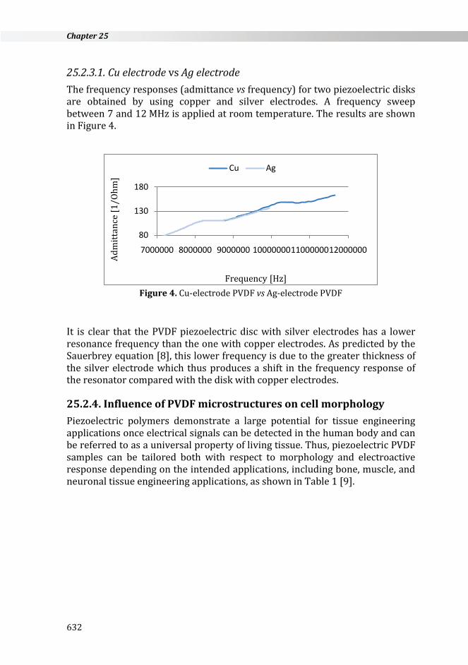
25.2.3.1. Cu electrode vs Ag electrode The frequency responses (admittance vs frequency) for two piezoelectric disks are obtained by using copper and silver electrodes. A frequency sweep between 7 and 12 MHz is applied at room temperature. The results are shown in Figure 4.
Figure 4. Cu-electrode PVDF vs Ag-electrode PVDF
It is clear that the PVDF piezoelectric disc with silver electrodes has a lower resonance frequency than the one with copper electrodes. As predicted by the Sauerbrey equation [8], this lower frequency is due to the greater thickness of the silver electrode which thus produces a shift in the frequency response of the resonator compared with the disk with copper electrodes.
25.2.4. Influence of PVDF microstructures on cell morphology Piezoelectric polymers demonstrate a large potential for tissue engineering applications once electrical signals can be detected in the human body and can be referred to as a universal property of living tissue. Thus, piezoelectric PVDF samples can be tailored both with respect to morphology and electroactive response depending on the intended applications, including bone, muscle, and neuronal tissue engineering applications, as shown in Table 1 [9].
80
130
180
7000000 8000000 9000000 100000001100000012000000
Adm
ittan
ce [1
/Ohm
]
Frequency [Hz]
Cu Ag
632

Acoustic wave resonators for biomedical applications
Table 1. Contact angle values (mean ± SD) of the different PVDF samples depending on microstructure and poling state and their potential applications in tissue engineering.
“Poled +” and “Poled −” means poled samples with a positive and negative surface charge, respectively.
PVDF samples Contact angle values
Applications in tissue engineering
non-poled β-PVDF films 83.1° ± 2.2°
bone
“poled +”β-PVDF films
51.3° ± 3.1°
muscle
“poled −”β-PVDF films
45.0° ± 1.6°
cartilage
β-PVDF porous membranes
94.3° ± 2.6°
neuronal
aligned β-PVDF fibres
135.1° ± 3.0°
spinal cord injury
random β-PVDF fibres
115.6° ± 3.3°
wound healing It has been shown that piezoelectric polymers allow appropriate design to develop novel and efficient tissue engineering strategies for cells that need electromechanical stimuli for their suitable development. In particular, suitable piezoelectric scaffolds can take advantage of the mechanical activity of tissues to generate the necessary varying electrical signals for proper tissue regeneration, as is the case for bone and muscle, which include electromechanical activity in their formation and normal activity.
25.2.5. More applications... Reis et al. presented preliminary results on the use of a piezoelectric actuator in an orthopaedic application [10]. The use of the converse piezoelectric effect to mechanically stimulate bone was achieved with PVDF actuators implanted in osteotomy cuts in a sheep femur and tibia (Figure 5).
Figure 5. Actuator position inside the tibia obtained post-mortem—scale bar 1 cm
633
Chapter 25
The bone deposition rate was significantly higher in the mechanicallystimulated areas. In these areas, increased osteopontin expression was observed. The present in vivo study suggests that piezoelectric materials and the converse piezoelectric effect may be used to effectively stimulate bone growth. Pärssinen et al. worked with nonelectroactive α-PVDF and electroactive β-PVDF to investigate the substrate polarisation and polarity influence on focal adhesion size and number as well as on human adipose stem cell differentiation [11]. The surface charge of the poled PVDF films (positive or negative) influenced the hydrophobicity of the samples, leading to variations in the conformation of adsorbed extracellular matrix proteins, which ultimately modulated the stem cell adhesion on the films, thus inducing their osteogenic differentiation.
25.3. BIOCOMPATIBLE ALN MEMBRANE Nowadays, the development of the thin-film bulk acoustic wave resonator (FBAR) is constantly growing. This technology was born as a direct extension of quartz crystal resonators. These are bulk acoustic wave (BAW)-based thickness mode wave resonators, permitting a reduction in the piezoelectric thickness of the implant and thus conducting an increased resonance frequency. Therefore, high s ensibility in gravimetric applications was reached in addition to their compatibility with integrated circuit (IC) technology. AlN is a piezoelectric material, previously primarily used in the electronics industry as a circuit substrate due to its relatively high thermal conductivity in combination with being an electrical insulator. It is a very attractive piezoelectric material for use in biomedical MEMS (BioMEMS) because it is biocompatible, exhibits high resistivity, high breakdown voltage, and high acoustic velocity, and it can be grown with the reactive sputtering technique at relatively low temperatures, thus making it compatible with integrated circuit technology. Material compatibility with integrated circuit fabrication opens the way for monolithic integration of the traditionally incompatible IC and electro-acoustic technologies. The most common materials for thin-film electro-acoustic devices today include AlN, ZnO, and lead zirconium titanate (PZT). Extensive research on and development of AlN thin-film synthesis for high frequency surface acoustic wave (SAW) and BAW applications has resulted in AlN so far appearing to be the best compromise between performance and manufacturability and the prime candidate for the mass production of FBARs and filters. Material compatibility with IC fabrication opens the way for monolithic integration of the traditionally incompatible IC and electro-acoustic technologies.
634

Acoustic wave resonators for biomedical applications
AlN is most often in the wurtzite hexagonal crystallographic system around the c-axis, which is also the direction with the highest piezoelectric constant in addition to a high acoustic wave velocity. Regarding the crystal structure of AlN, there are two main crystallographic orientations that provide piezoelectric behaviour. The crystallographic orientation (002) has the highest piezoelectric constant and has a diffraction peak at 36°, while the crystallographic orientation (100) has a diffraction peak at 33°. This section deals with the deposition of AlN on a silicon substrate, where the feasibility of the final goal of fabricating unconventional piezoelectric materials for biomedical applications is shown.
25.3.1. Deposition process A Pt layer is grown with magnetron sputter deposition on top of a Ti film deposited on a SiO2 surface as an adhesion layer. The Pt bottom electrode is grown with sputter deposition. A Ti film provides an adhesion layer for growing highly c-axis (002) oriented AlN films. The thicknesses of the Pt and Ti is 150 nm and 10 nm, respectively. In addition, this coating provides seeding capability and serves as a buffer layer, lowering the discrepancy in the lattice parameter between substrate and film. The Pt layer will serve as the bottom and top electrode to apply voltage to excite the piezoelectric if that is required. A scheme of the used piezoelectric heterostructure is shown in Figure 6.
Figure 6. Scheme of the heterostructure of AlN/Pt/Ti/SiO2/Si
AlN (002)-oriented films are grown on the Pt layers using reactive sputter deposition, via sputtering material from an Al metallic target, using an Ar-plasma to produce Ar ions to sputter the Al material in a N2 atmosphere to provide the nitrogen needed for the AlN films.
635
Chapter 25
25.3.2. Characterisation A straightforward way to discover the crystalline structure of a material and its preferential orientation is by using X-ray diffraction (XRD). It is a nondestructive technique that reveals detailed information about the chemical composition and the crystalline structure of a material. Atoms in a material are organised in a 3D arrangement forming a series of parallel planes separated by a distance that depends on the nature of the material. When a monochromatic X-ray beam is projected on the material, a diffraction pattern according to Bragg’s Law is obtained:
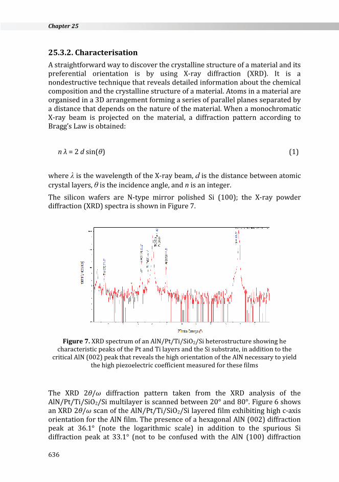
n λ = 2 d sin(θ) (1) where λ is the wavelength of the X-ray beam, d is the distance between atomic crystal layers, θ is the incidence angle, and n is an integer. The silicon wafers are N-type mirror polished Si (100); the X-ray powder diffraction (XRD) spectra is shown in Figure 7.
Figure 7. XRD spectrum of an AlN/Pt/Ti/SiO2/Si heterostructure showing he
characteristic peaks of the Pt and Ti layers and the Si substrate, in addition to the critical AlN (002) peak that reveals the high orientation of the AlN necessary to yield
the high piezoelectric coefficient measured for these films
The XRD 2θ/ω diffraction pattern taken from the XRD analysis of the AlN/Pt/Ti/SiO2/Si multilayer is scanned between 20° and 80°. Figure 6 shows an XRD 2θ/ω scan of the AlN/Pt/Ti/SiO2/Si layered film exhibiting high c-axis orientation for the AlN film. The presence of a hexagonal AlN (002) diffraction peak at 36.1° (note the logarithmic scale) in addition to the spurious Si diffraction peak at 33.1° (not to be confused with the AlN (100) diffraction
636
Acoustic wave resonators for biomedical applications
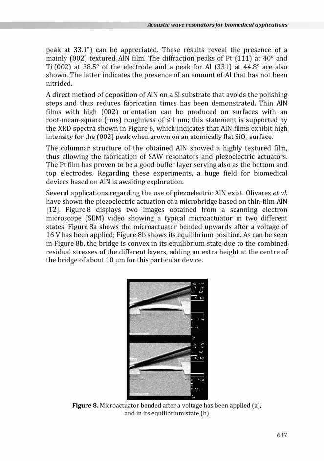
peak at 33.1°) can be appreciated. These results reveal the presence of a mainly (002) textured AlN film. The diffraction peaks of Pt (111) at 40° and Ti (002) at 38.5° of the electrode and a peak for Al (331) at 44.8° are also shown. The latter indicates the presence of an amount of Al that has not been nitrided. A direct method of deposition of AlN on a Si substrate that avoids the polishing steps and thus reduces fabrication times has been demonstrated. Thin AlN films with high (002) orientation can be produced on surfaces with an root-mean-square (rms) roughness of ≤ 1 nm; this statement is supported by the XRD spectra shown in Figure 6, which indicates that AlN films exhibit high intensity for the (002) peak when grown on an atomically flat SiO2 surface. The columnar structure of the obtained AlN showed a highly textured film, thus allowing the fabrication of SAW resonators and piezoelectric actuators. The Pt film has proven to be a good buffer layer serving also as the bottom and top electrodes. Regarding these experiments, a huge field for biomedical devices based on AlN is awaiting exploration. Several applications regarding the use of piezoelectric AlN exist. Olivares et al. have shown the piezoelectric actuation of a microbridge based on thin-film AlN [12]. Figure 8 displays two images obtained from a scanning electron microscope (SEM) video showing a typical microactuator in two different states. Figure 8a shows the microactuator bended upwards after a voltage of 16 V has been applied; Figure 8b shows its equilibrium position. As can be seen in Figure 8b, the bridge is convex in its equilibrium state due to the combined residual stresses of the different layers, adding an extra height at the centre of the bridge of about 10 μm for this particular device.
Figure 8. Microactuator bended after a voltage has been applied (a),
and in its equilibrium state (b)
637

Chapter 25
The authors have demonstrated the viability of using piezoelectric AlN for the actuation of suspended microbridges. The microbridges achieved a deflection of up to 0.22 μm V−1; this actuation response is sufficiently good for Radio Frequency (RF) microswitching applications. Furthermore, Sinha et al. reported AlN films with nanoscale thickness for nanoelectromechanical systems (NEMS) switches [13]. The nanoactuator shown in Figure 9 was fabricated as a beam clamped at both ends and successively cut by a focused ion beam to free one end and test different length structures as bending cantilevers. The actuation voltage can be applied to each of the two piezoelectric layers separately and consequently permits the nanomechanical actuator to operate as a unimorph or as a bimorph structure. Results lead to the demonstration of bimorph actuation at the nanoscale using AlN piezoelectric films that have preserved the same stress-free state and high piezoelectric coefficients as their macroscopic counterparts.
Figure 9. The sample was tilted to provide a 3D view of the nanoactuator and to show
its constituent layers: a 350 nm-thick stack formed by two 100 nm-thick AlN layers and three 50 nm-thick Pt layers. The released cantilevered beam also shows very small out-of-plane deflections. This is indicative of low levels of stress gradients in the nano-
AlN films. The inset schematic illustrates a cross-sectional view of the stack of layers used to make the device and the operating principle of the bimorph nanoactuator.
Furthermore, Iborra et al. demonstrated the fabrication of micromachined suspended bridge structures formed by AlN/polysilicon bimorphs [14].
638
Acoustic wave resonators for biomedical applications
25.4. AlN AND UNCD... A PROMISE BioMEMS technology has been inherited from the IC Industry and has resulted from the integration of structural and functional microparts such as microchannels, microreservoirs, microsensors, and microactuators. It has recently been developed to overcome several limitations imposed by the current state of the art in medical technology. In spite of the remarkable advantages that BioMEMS technology brings, the need still exists for a biocompatible–bioinert material capable of persisting in the harsh environment of the human body without suffering from biofouling and that is capable of sustaining microfabrication processes while keeping its properties intact. In this sense, AlN and diamond have been demonstrated to accomplish these aspects. The fabrication of diamond-based devices requires the growth of diamond films on appropriate substrates followed by photolithography and etching to release moving structures, for example cantilevers and beams. Ultrananocrystalline diamond (UNCD) exhibits superior mechanical/tribological properties combined with smoother surface morphology (~4–7 nm rms roughness) and the lowest diamond deposition temperature demonstrated today (400 °C) compared with single crystal diamond, microcrystalline diamond, nanocrystalline diamond (NCD), and diamond-like films [15,16]. UNCD films are grown on substrates exposed to Ar-rich CH4 microwave plasma (MPCVD) which yields 2–5 nm diamond grains and 0.4 nm-wide grain boundaries with sp3 and sp2 bondings. This nanostructure provides the name UNCD for distinction from NCD films grown with H-rich/CH4 plasmas that yield films with 30–100 nm grain sizes. UNCD exhibits a unique combination of high fracture strength (~5.4 GPa) and Young’s modulus (~990 GPa), low stress (~50–80 MPa), negligible stiction, exceptional chemical inertness, high electric field-induced electron emission, and surface functionalisation that makes it bioinert/biocompatible for applications in biosensors and biomedical devices. For example, UNCD has been developed as a hermetic bioinert/biocompatible encapsulating coating for a Si microchip [17]. In that work, in vivo passive evaluation of UNCD-coated samples implanted in the eyes of rabbits were reported; six-months tests involving the implantation of UNCD-coated Si chips in the eyes of a pigmented rabbit demonstrated that UNCD is bioinert and biostable, thus evidencing the potential of low-temperature UNCD as a hermetic coating on implantable retinal microchips. Following the implantation of the samples in the eyes of rabbits, no evidence of inflammation above and beyond was noted. As shown in Figure 10, there was no evidence of acute damage of the surface.
639
Chapter 25
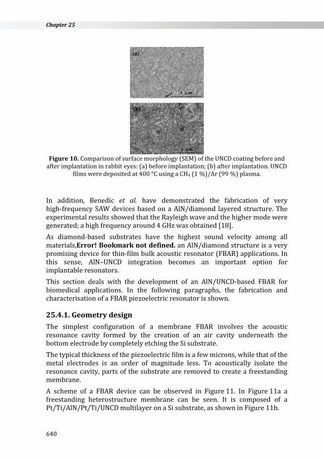
Figure 10. Comparison of surface morphology (SEM) of the UNCD coating before and
after implantation in rabbit eyes: (a) before implantation; (b) after implantation. UNCD films were deposited at 400 °C using a CH4 (1 %)/Ar (99 %) plasma.
In addition, Benedic et al. have demonstrated the fabrication of very high-frequency SAW devices based on a AlN/diamond layered structure. The experimental results showed that the Rayleigh wave and the higher mode were generated; a high frequency around 4 GHz was obtained [18]. As diamond-based substrates have the highest sound velocity among all materials,Error! Bookmark not defined. an AlN/diamond structure is a very promising device for thin-film bulk acoustic resonator (FBAR) applications. In this sense, AlN–UNCD integration becomes an important option for implantable resonators. This section deals with the development of an AlN/UNCD-based FBAR for biomedical applications. In the following paragraphs, the fabrication and characterisation of a FBAR piezoelectric resonator is shown.
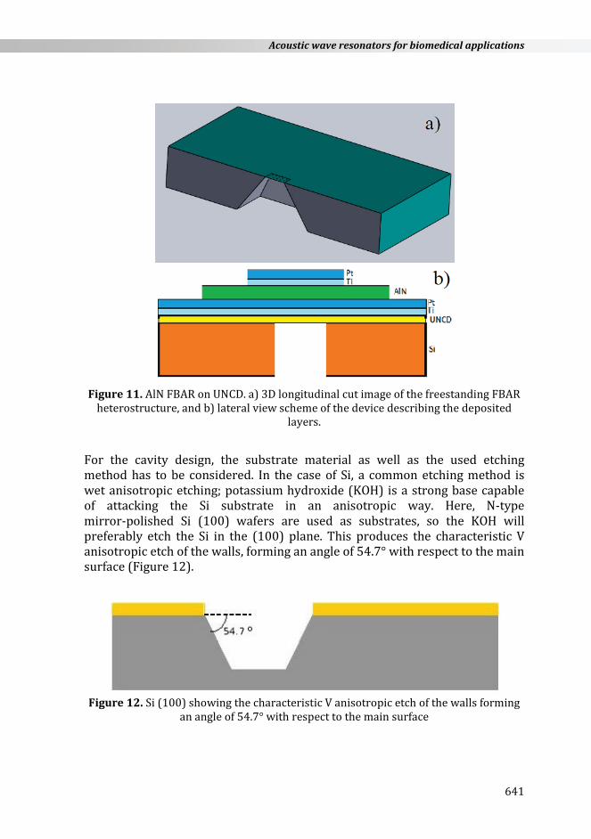
25.4.1. Geometry design The simplest configuration of a membrane FBAR involves the acoustic resonance cavity formed by the creation of an air cavity underneath the bottom electrode by completely etching the Si substrate. The typical thickness of the piezoelectric film is a few microns, while that of the metal electrodes is an order of magnitude less. To acoustically isolate the resonance cavity, parts of the substrate are removed to create a freestanding membrane. A scheme of a FBAR device can be observed in Figure 11. In Figure 11a a freestanding heterostructure membrane can be seen. It is composed of a Pt/Ti/AlN/Pt/Ti/UNCD multilayer on a Si substrate, as shown in Figure 11b.
640
Acoustic wave resonators for biomedical applications
Figure 11. AlN FBAR on UNCD. a) 3D longitudinal cut image of the freestanding FBAR
heterostructure, and b) lateral view scheme of the device describing the deposited layers.
For the cavity design, the substrate material as well as the used etching method has to be considered. In the case of Si, a common etching method is wet anisotropic etching; potassium hydroxide (KOH) is a strong base capable of attacking the Si substrate in an anisotropic way. Here, N-type mirror-polished Si (100) wafers are used as substrates, so the KOH will preferably etch the Si in the (100) plane. This produces the characteristic V anisotropic etch of the walls, forming an angle of 54.7° with respect to the main surface (Figure 12).
Figure 12. Si (100) showing the characteristic V anisotropic etch of the walls forming
an angle of 54.7° with respect to the main surface
641
Chapter 25
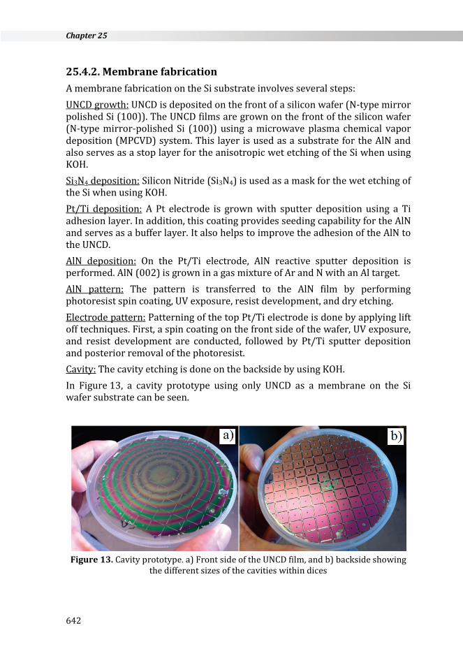
25.4.2. Membrane fabrication A membrane fabrication on the Si substrate involves several steps: UNCD growth: UNCD is deposited on the front of a silicon wafer (N-type mirror polished Si (100)). The UNCD films are grown on the front of the silicon wafer (N-type mirror-polished Si (100)) using a microwave plasma chemical vapor deposition (MPCVD) system. This layer is used as a substrate for the AlN and also serves as a stop layer for the anisotropic wet etching of the Si when using KOH. Si3N4 deposition: Silicon Nitride (Si3N4) is used as a mask for the wet etching of the Si when using KOH. Pt/Ti deposition: A Pt electrode is grown with sputter deposition using a Ti adhesion layer. In addition, this coating provides seeding capability for the AlN and serves as a buffer layer. It also helps to improve the adhesion of the AlN to the UNCD. AlN deposition: On the Pt/Ti electrode, AlN reactive sputter deposition is performed. AlN (002) is grown in a gas mixture of Ar and N with an Al target. AlN pattern: The pattern is transferred to the AlN film by performing photoresist spin coating, UV exposure, resist development, and dry etching. Electrode pattern: Patterning of the top Pt/Ti electrode is done by applying lift off techniques. First, a spin coating on the front side of the wafer, UV exposure, and resist development are conducted, followed by Pt/Ti sputter deposition and posterior removal of the photoresist. Cavity: The cavity etching is done on the backside by using KOH. In Figure 13, a cavity prototype using only UNCD as a membrane on the Si wafer substrate can be seen.
Figure 13. Cavity prototype. a) Front side of the UNCD film, and b) backside showing
the different sizes of the cavities within dices
642

Acoustic wave resonators for biomedical applications
25.4.3. Device characterisation
25.4.3.1. X-ray diffraction (XRD) Figure 14 shows an XRD θ–2θ scan of the AlN/Pt/Ti/UNCD/SiO2/Si layered film exhibiting high c-axis orientation for the AlN film. The presence of a hexagonal AlN (002) diffraction peak at 36.05° can be noted, revealing the presence of a mainly (002)-textured AlN film. Further, two Pt peaks, (111) at 40.05° and (002) at 46.5°, are present. The weak peaks at 44.7° and at 65.1° correspond to Al (002) and Al (202), respectively. The strong narrow peak at 33.2° comes from the Si wafer substrate and is the result of Si crystalline imperfections.
Figure 14. XRD spectrum of an AlN/Pt/Ti/UNCD/SiO2/Si heterostructure showing the
characteristic peaks of the Pt layers and Si substrate, in addition to the critical AlN (002) peak that reveals the high orientation of the AlN necessary to yield the high
piezoelectric coefficient
The X-ray wavelength was λ = 1.540598 Å and by using Bragg’s law the c-lattice constant for the AlN layer could be calculated. The obtained value was 4.9681 Å which is in good agreement with the value of the AlN found elsewhere.
25.4.3.2. Scanning Electron Microscope (SEM) The SEM is today a routinely used instrument for the examination of fine detail for a variety of samples. The instrument is, in simple terms, analogous to an optical microscope: the electron source (gun) is equivalent to the light source and the glass lens is replaced by electromagnetic lens. Information from the sample is collected and displayed on a viewing screen for visual interpretation.
643
Chapter 25
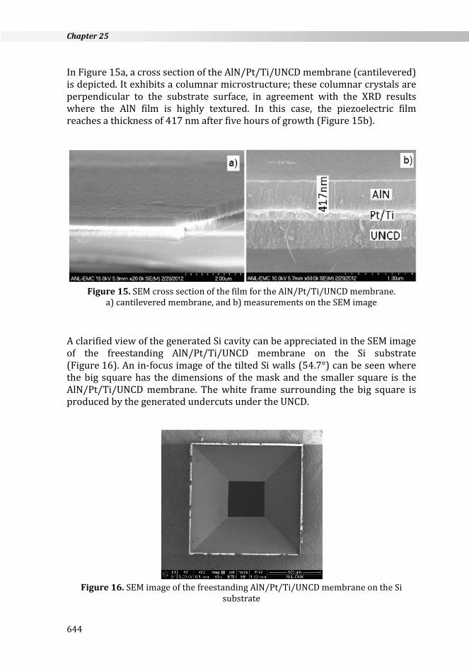
In Figure 15a, a cross section of the AlN/Pt/Ti/UNCD membrane (cantilevered) is depicted. It exhibits a columnar microstructure; these columnar crystals are perpendicular to the substrate surface, in agreement with the XRD results where the AlN film is highly textured. In this case, the piezoelectric film reaches a thickness of 417 nm after five hours of growth (Figure 15b).
Figure 15. SEM cross section of the film for the AlN/Pt/Ti/UNCD membrane.
a) cantilevered membrane, and b) measurements on the SEM image
A clarified view of the generated Si cavity can be appreciated in the SEM image of the freestanding AlN/Pt/Ti/UNCD membrane on the Si substrate (Figure 16). An in-focus image of the tilted Si walls (54.7°) can be seen where the big square has the dimensions of the mask and the smaller square is the AlN/Pt/Ti/UNCD membrane. The white frame surrounding the big square is produced by the generated undercuts under the UNCD.
Figure 16. SEM image of the freestanding AlN/Pt/Ti/UNCD membrane on the Si
substrate
644

Acoustic wave resonators for biomedical applications
The low temperature of the UNCD growth in addition to the AlN deposition makes this innovative system compatible with CMOS chips and CMOS-driven MEMS and NEMS systems. Successful integration of piezoelectric AlN and UNCD films may enable the development of a new generation of biocompatible piezoelectric-based drug delivery MEMS devices that will be implantable in the human body. The feasibility of the fabrication of a FBAR AlN/diamond structure is a very promising device for FBAR applications, opening a huge field of biomedical applications.
25.5. COMPARISON TABLE Table 2 summarises the different developed biomedical systems.
Table 2. Summary of the biomedical systems analysed
System Piezo material Fabrication
Bioc
ompa
tible
?
IC C
ompa
tible
? Application
polymer-based
electroactive device
PVDF melt extrusion followed by stretching step and exposed to very high
electric fields Yes No
– tissue engineering – orthopaedics
– osteogenic differentiation
thin-film electroactive
device AlN magnetron sputter
deposition Yes Yes
– AlN thin-film-based microbridge
– NEMS switches. – micromachined suspended bridge
structures
AlN/UNCD-based
BioMEMS AlN magnetron sputter
deposition + MPCVD Yes Yes
– hermetic biocompatible
encapsulating coating for Si-microchips
– AlN/diamond-based SAW devices.
– FBAR piezoelectric resonators
645
Chapter 25
REFERENCES 1. A. Arnau, Piezoelectric transducers and applications, Springer Verlag, 2008. 2. J. Rosenbaum, Bulk Acoustic Wave Theory and Devices, Artech House, Inc.,
2000. 3. M. Koucky, Piezoelectric Polymer Microstructures For Biomedical Applications,
MS Thesis, The Ohio State University, 2009. 4. G. Ciofani, S. Danti, L. Ricotti, D.D. Alessandro, S. Moscato, V. Mattoli, in
Piezoelectric Nanomaterials for Biomedical Applications, G. Ciofani, A. Menciassi (Eds.), Springer, Germany, 2012, p.p. 213–238.
5. G.V. Cochran, M.P. Kadaba, V.R. Palmieri. J. Orthop. Res. 6 (1988) 145–147. 6. J. Rosenbaum, Bulk Acoustic Wave Theory and Devices, Artech House, Inc.,
2000. 7. Measurement Specialities, http://www.meas-spec.com/ (2015). 8. G. Sauerbrey. Z. Phys. 155 (1959) 206–222. 9. C. Ribeiro, D.M. Correia, S. Ribeiro, V. Sencadas, G. Botelho, S. Lanceros-
Méndez. Eng. Life Sci. 15(4) (2015) 351–356. 10. J. Reis, C. Frias, C.C. e Castro, M.L. Botelho, A.T. Marques, J.A. Oliveira Simões,
F.C. e Silva, J. Potes. J. Biomed. Biotechnol. 2012 (2012) 613403. 11. J. Pärssinen, H. Hammarén, R. Rahikainen, V. Sencadas, C. Ribeiro, S.
Vanhatupa, S. Miettinen, S. Lanceros‐Méndez, P. Hytönen Vesa. J. Biomed. Mater. Res. Part A 103(3) (2015) 919–928.
12. J. Olivares, E. Iborra, M. Clement, L. Vergara, J. Sangrador, A. Sanz-Hervás. Sensor. Actuat. A: Phys. 123-124 (2005) 590–595.
13. N. Sinha, G.E. Wabiszewski, R. Mahameed, V.V. Felmetsger, S.M. Tanner, R.W. Carpick. Departmental Papers (MEAM) (2009) 165.
14. E. Iborrra, J. Olivares, M. Clement. L. Vergara, A. Sanz-Hervas, J. Sangrador. Sensor. Actuat. A: Phys. 115(2-3) (2004) 501–507.
15. O. Auciello, J. Birrell, J.A. Carlisle, J.E Gerbi, X. Xiao, B. Peng, H.D. Espinosa. J. Phys.: Condens. Matter 16(16) (2004) R539.
16. O. Auciello, A.V. Sumant. Diam. Relat. Mater. 19(7) (2010) 699–718. 17. X. Xiao, J. Wang, C. Liu, J.A. Carlisle, B. Mech, R. Greenberg, D. Guven, R. Freda,
M.S. Humayun, J. Weiland, O. Auciello. J. Biomed. Mater. Res. Part B: Appl. Biomater. 77(2) (2006) 273–281.
18. F. Benedic, M.B. Assouar, P. Kirsch, D. Moneger, O. Brinza, O. Elmazria, P. Alnot, A. Gicquel. Diam. Relat. Mater. 17(4) (2008) 804–808.
646