click valates a - maxim integrated
TRANSCRIPT

Evaluates: MAX25202MAX25202 Evaluation Kit
General DescriptionThe MAX25202 evaluation kit (EV kit) is a fully assembled and tested application circuit that simplifies the evalu-ation of the MAX25202 400kHz, 36V boost controller. All installed components are rated for the automotive temperature range. Various test points and jumpers are included for evaluation.The standard EV kit comes with the installed MAX25202 (24V, 400kHz) and can also be used to evaluate other MAX25202 variants with minimal component changes shown in the MAX25202 EV Kit Bill of Materials.
Benefits and Features● 4.5V to 36V Input Supply Range● Input Voltage Range Extended Down to 2V after
Initial Startup● Boost Output Voltages Adjustable between 4.5V and
60V via External Resistors● Boost Fixed Output Voltage Available with Minor
Component Changes● ±2% Output Voltage Accuracy● Frequency-Synchronization Input● Enable Input● Voltage-Monitoring PGOOD Output● Jumpers and Test Points on Key Nodes for Simplified
Evaluation● Proven PCB Layout● Fully Assembled and Tested
319-100592; Rev 0; 9/20
Ordering Information appears at end of data sheet.
Quick StartRequired Equipment● MAX25202 EV kit● 30V, 25A DC power supply (PS1)● One voltmeter (VM1)● One electronic load, 200W capable (EL1)
ProcedureThe EV kit is fully assembled and tested. Follow the steps below to verify board operation.Caution: Do not turn on the power supply until all connections are completed.1) Verify that all jumpers are in their default positions as
shown in Table 1.2) Preset the output voltage of PS1 to 14V. Disable
PS1 output.3) Turn off the EL1 and preset the load to 8A.4) Connect the positive terminal of EL1 to the OUT
screw terminal; connect the negative terminal of EL1to GND2 screw terminal.
5) Connect the positive terminal of PS1 to the SUPscrew terminal; connect the negative terminal of PS1to GND1 screw terminal.
6) Connect the positive terminal of VM1 to the OUT testpoint loop; connect the negative terminal of VM1 tothe GND2 test point loop.
7) Enable the power supply output.8) Enable the electronic load EL1.9) Verify that the voltmeter on OUT measures approxi-
mately 24V.
Click here to ask about the production status of specific part numbers.
Maxim Integrated │ 2www.maximintegrated.com
Evaluates: MAX25202MAX25202 Evaluation Kit
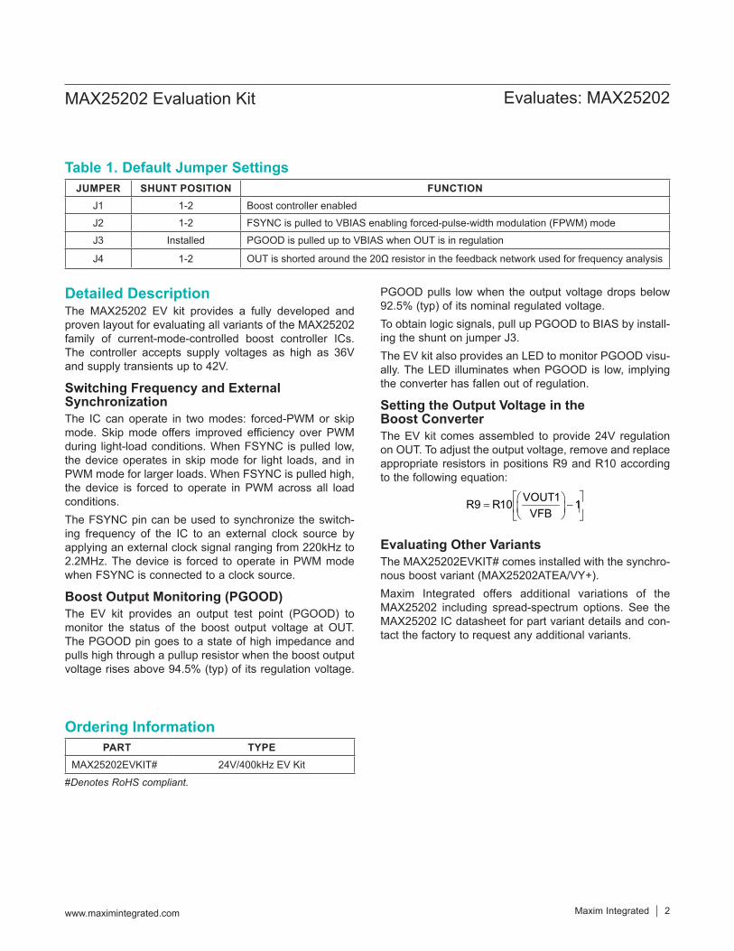
Detailed DescriptionThe MAX25202 EV kit provides a fully developed and proven layout for evaluating all variants of the MAX25202 family of current-mode-controlled boost controller ICs. The controller accepts supply voltages as high as 36V and supply transients up to 42V.
Switching Frequency and External SynchronizationThe IC can operate in two modes: forced-PWM or skip mode. Skip mode offers improved efficiency over PWM during light-load conditions. When FSYNC is pulled low, the device operates in skip mode for light loads, and in PWM mode for larger loads. When FSYNC is pulled high, the device is forced to operate in PWM across all load conditions. The FSYNC pin can be used to synchronize the switch-ing frequency of the IC to an external clock source by applying an external clock signal ranging from 220kHz to 2.2MHz. The device is forced to operate in PWM mode when FSYNC is connected to a clock source.
Boost Output Monitoring (PGOOD) The EV kit provides an output test point (PGOOD) to monitor the status of the boost output voltage at OUT. The PGOOD pin goes to a state of high impedance and pulls high through a pullup resistor when the boost output voltage rises above 94.5% (typ) of its regulation voltage.
PGOOD pulls low when the output voltage drops below 92.5% (typ) of its nominal regulated voltage.To obtain logic signals, pull up PGOOD to BIAS by install-ing the shunt on jumper J3.The EV kit also provides an LED to monitor PGOOD visu-ally. The LED illuminates when PGOOD is low, implying the converter has fallen out of regulation.
Setting the Output Voltage in the Boost ConverterThe EV kit comes assembled to provide 24V regulation on OUT. To adjust the output voltage, remove and replace appropriate resistors in positions R9 and R10 according to the following equation:
VOUT1R9 R10 1VFB
= −
Evaluating Other VariantsThe MAX25202EVKIT# comes installed with the synchro-nous boost variant (MAX25202ATEA/VY+).Maxim Integrated offers additional variations of the MAX25202 including spread-spectrum options. See the MAX25202 IC datasheet for part variant details and con-tact the factory to request any additional variants.
Table 1. Default Jumper Settings
#Denotes RoHS compliant.
JUMPER SHUNT POSITION FUNCTIONJ1 1-2 Boost controller enabledJ2 1-2 FSYNC is pulled to VBIAS enabling forced-pulse-width modulation (FPWM) modeJ3 Installed PGOOD is pulled up to VBIAS when OUT is in regulation
J4 1-2 OUT is shorted around the 20Ω resistor in the feedback network used for frequency analysis
PART TYPEMAX25202EVKIT# 24V/400kHz EV Kit
Ordering Information

Maxim Integrated │ 3www.maximintegrated.com
Evaluates: MAX25202MAX25202 Evaluation Kit
MAX25202 EV Kit Bill of MaterialsITEM QTY REF DES MFG PART # MANUFACTURER VALUE DESCRIPTION COMMENTS
1 9BIAS, FSYNCIN, GND1-GND4, OUT, PGOOD, SUP
9020 BUSS WEICO WIRE MAXIMPADEVK KIT PARTS; MAXIM PAD; WIRE; NATURAL; SOLID; WEICO WIRE; SOFT DRAWN BUS TYPE-S; 20AWG
2 2 C1, C22 EEE-FP1H101AP PANASONIC 100UF CAP; SMT (CASE_F); 100UF; 20%; 50V; ALUMINUM-ELECTROLYTIC
3 6 C3, C4, C11, C40, C46, C47 CGA5L3X7R1H475K160AB TDK 4.7UFCAPACITOR; SMT (1206); CERAMIC CHIP; 4.7UF ; 50V; TOL=10%; TG=-55 DEGC TO +125 DEGC; TC=X7R; AUTO
C5, C19, C26, C27 0.015uF
4 2 C6, C33 CGA4J3X7R1H225K125AB TDK 2.2UFCAPACITOR; SMT (0805); CERAMIC CHIP; 2.2UF; 50V; TOL=10%; TG=-55 DEGC TO +125 DEGC; TC=X7R; AUTO
5 1 C7 CGA3E2C0G1H100D080AA TDK 10PF CAP; SMT (0603); 10PF; +/-0.50PF; 50V; C0G; CERAMIC CHIP; AUTO
6 1 C8 0.012UF
7 2 C9, C32 CGA3E3X7S2A104K080AB TDK 0.1UFCAPACITOR; SMT (0603); CERAMIC CHIP; 0.1UF; 100V; TOL=10%; TG=-55 DEGC TO +125 DEGC; TC=X7S
8 1 C10 GCM188R71H473KA55;CGA3E2X7R1H473K080AA MURATA;TDK 0.047UF
CAPACITOR; SMT (0603); CERAMIC CHIP; 0.047UF; 50V; TOL=10%; MODEL=; TG=-55 DEGC TO +125 DEGC; TC=X7R; NOTE: AUTOMOTIVE PART ONLY
9 6 C16, C24, C25, C48, C49, C51
EEH-ZC1H121P PANASONIC 120UF CAP; SMT (CASE_G); 120UF; 20%; 50V; ALUMINUM-ELECTROLYTIC
C39, C50 DNI
10 2 C17, C34 CGA2B1X7R1C104K050BC; GCM155R71C104KA55 TDK;MURATA 0.1UF
CAPACITOR; SMT (0402); CERAMIC CHIP; 0.1UF; 16V; TOL=10%; TG=-55 DEGC TO +125 DEGC; TC=X7R; AUTO
C18, C29 4700pF
11 1 C41 GCM1555C1H220JA16 MURATA 22PFCAPACITOR; SMT (0402); CERAMIC CHIP; 22PF; 50V; TOL=5%; TG=-55 DEGC TO +125 DEGC; TC=C0G; NOTE: AUTOMOTIVE PART ONLY
12 2 D1, D2 1N4148WS-7-F DIODES INCORPORATED 1N4148WS-7-F DIODE; SWT; SMT (SOD-323); PIV=75V; IF=0.3A
13 1 DS1 LTST-C190KRKT LITE-ON ELECTRONICS INC. LTST-C190KRKT DIODE; LED; ULTRA BRIGHT AlInCaP CHIP LED; RED; SMT; VF=2V; IF=0.025A
14 2 J1, J2 PBC03SAAN SULLINS PBC03SAANCONNECTOR; MALE; THROUGH HOLE; BREAKAWAY; STRAIGHT; 3PINS; -65 DEGC TO +125 DEGC
15 1 J3 TSW-102-07-T-S SAMTEC TSW-102-07-T-SCONNECTOR; THROUGH HOLE; TSW SERIES; SINGLE ROW; STRAIGHT; 2PINS; -55 DEGC TO +105 DEGC
16 2 L1, L2 XAL1060-222ME COILCRAFT 2.2UHINDUCTOR; SMT; COMPOSITE; 2.2UH; 20%; 20A; NOTE: SET TO OBSOLETE FOR FOOTPRINT CORRECTION BASED ON LATEST DATASHEET
17 4 MH1-MH4 9032 KEYSTONE 9032 MACHINE FABRICATED; ROUND-THRU HOLE SPACER; NO THREAD; M3.5; 5/8IN; NYLON
18 6 Q1-Q3, Q5-Q7 DMTH6009LPS DIODES INCORPORATED DMTH6009LPS TRAN; NCH; ENHANCEMENT MODE MOSFET; POWERDI5060-8; PD-(2.8W); I-(11.76A); V-(60V)
Q4, Q8 DNI
19 2 R1, R5 PML100HZPJV1L5 ROHM SEMICONDUCTOR 0.0015 RES; SMT (1225); 0.0015; 5%; +/-100PPM/DEGC; 2W
20 1 R2 39k
21 1 R19 CRCW06030000ZS;MCR03EZPJ000;ERJ-3GEY0R00 VISHAY DALE;ROHM;PANASONIC 0 RESISTOR; 0603; 0 OHM; 0%; JUMPER; 0.10W;
THICK FILM
8 R3, R4, R7, R8, R13, R11, R17, R18
1
22 1 R9 CRCW0603115KFK VISHAY 115K RES; SMT (0603); 115K; 1%; +/-100PPM/DEGC; 0.1W
23 1 R10 CRCW06034K99FK;ERJ-3EKF4991V VISHAY DALE;PANASONIC 4.99K RESISTOR; 0603; 4.99K; 1%; 100PPM; 0.10W; THICK FILM
24 1 R14 CRCW060320R0FK; ERJ-3EKF20R0V VISHAY DALE;PANASONIC 20 RESISTOR, 0603, 20 OHM, 1%, 100PPM, 0.10W, THICK FILM
25 1 R20 CRCW06031K00FK;ERJ-3EKF1001V VISHAY DALE;PANASONIC 1K RESISTOR; 0603; 1K; 1%; 100PPM; 0.10W; THICK FILM
26 1 R21 CRCW060310K0FK;ERJ-3EKF1002 VISHAY DALE;PANASONIC 10K RESISTOR; 0603; 10K; 1%; 100PPM; 0.10W; THICK FILM
27 3 SU1-SU3 SNT-100-BK-G SAMTEC SNT-100-BK-G
TEST POINT; SHUNT AND JUMPER; STR; TOTAL LENGTH=6.10MM; BLACK; INSULATION=GLASS FILLED POLYESTER; CONTACT=PHOSPHOR BRONZE
28 1 U1 MAX25202MATEA/VY+ MAXIM MAX25202MATEA/VY+
EVKIT PART - IC; MAX25202MATEA/VY+; 16L WETQFN; PACKAGE OUTLINE DRAWING: 21-100108; LAND PATTERN NUMBER: 90-100046; PACKAGE CODE: T1633Y+4C
29 1 U2 MAX25202SATEA/VY+ MAXIM MAX25202SATEA/VY+
EVKIT PART - IC; MAX25202SATEA/VY+; 16L WETQFN; PACKAGE OUTLINE DRAWING: 21-100108; LAND PATTERN NUMBER: 90-100046;PACKAGE CODE: T1633Y+4C
30 1 PCB MAX25202EVK MAXIM PCB PCB:MAX25202EVK -
TOTAL 78

Maxim Integrated │ 4www.maximintegrated.com
Evaluates: MAX25202MAX25202 Evaluation Kit
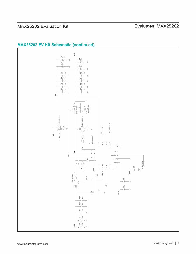
MAX25202 EV Kit Schematic
PWM
SKIP
OPE
N=E
XTER
NAL
FSY
NC
OFF
LED
ON
0.04
7UF
50V
PBC
03SA
AN
1210
2 1
J5
2 1
J6
3
2
1
J4
KA
C2
KA
C1
C11
KA
C39
KA
C24
KA
C25
KA
C16
R14
C28
C30
C31
C20
C17
KA
DS1
PGO
OD
21
J3
R20
R21
3
2
1
J2
321
4
5
Q3
C21
C19
C5
R13
C18
R11
R2
C7
C8
C3
GN
D4
R9
C15
C14
C13
C12
R6
C4
GN
D3
GN
D2
GN
D1
OU
TSU
P
BIAS
C10
FSYN
CIN
R1
3
2
1
J1
R10
3
21
D3
C6
R3
R4
321
4
5
Q1
321
4
5
Q2
CBI
ASM A
D2
C9
21
L1
17
16
15
14
13
1211
10
9
8
7
6
5
43
21
U1
OSTYK44102030
0M
AX25
202M
ATEA
/VY+
OST
YK44
1020
30
1210
10U
F
115K
BIAS
M
50V
10U
F12
10
NVM
FS5C
670N
LWFA
FT1G
10PF
PBC
03SA
AN
BIAS
M
10U
F12
1010
UF
50V
50V
FBR
20
4.99
K
4.7U
F
120U
F
50V
120U
F
50V
LXM
0.00
2
0
0
50V
BIAS
M
1K2.
2UF0
10U
F
0.1U
F
TSW
-102
-07-
T-S
1210
1210
1210
10U
F
50V
0
4.7U
F
10K
50V
50V
120U
F
0.1U
F
39.2
K
2.2U
H
CO
MP
DLM
DLM
G
PMEG
060V
100E
PD
SS
50V
50V
OU
T
DLM
G
50V
120U
F
OU
T
10U
F
50V
10U
F
50V
120U
F12
10
NVM
FS5C
670N
LWFA
FT1G
LXM
PBC
03SA
AN
BIAS
M
NVM
FS5C
670N
LWFA
FT1G
DH
M
120U
F
FSYN
CO
UTM
FB
BSTM
EN
SUP_
M
CSM
1N41
48W
S-7-
F
XAL1
010-
222M
E
4.7U
F
50V
SUP
50V
PGO
OD
LTST
-C19
0KR
KT
FSYN
CIN
/MO
DE
0.01
2UF
S
D
G
+
SD
G
SD
G
AA
C
+
+
+
+
+
EP
EN
BST
LX
DH
GN
DDL
BIAS
FSYN
CO
UT
FSYNCIN
PGOOD
SS
COMP
FB
OU
T
SUP
CS
Maxim Integrated │ 5www.maximintegrated.com
Evaluates: MAX25202MAX25202 Evaluation Kit
MAX25202 EV Kit Schematic (continued)
KA
C23
KA
C22
KA
C49
KA
C51
KA
C48
KA
C50
C40
C47
C46
C41
C43
C44
C45
C42
C33
C34
1716
15
14
13
12
11
10
9
8
7
6
5
43
21
U2
R19
C27
C38
C37
C36
C35
321
4
5
Q7
321
4
5
Q6
R18
3
21
D4
321
4
5
Q5
C32
CA
D1
21
L2
R8
R5
R17
C29
R7 C
26
120U
F
LXS
NVM
FS5C
670N
LWFA
FT1G
DH
S
4.7U
F4.
7UF
120U
F
50V
4.7U
F
50V
50V
120U
F
50V
120U
F
OU
T
FB
10U
F
50V
OU
T
DLS
G
2.2U
F
CO
MP
BIAS
S
22PF
50V
50V
50V
1210
10U
F12
10
1210
10U
F10
UF
1210
10U
F
FSYN
CO
UTM
1210
50V
50V
120U
F
0.1U
F
LXS
50V
10U
F
50V
50V
120U
F
1210
50V
0
NVM
FS5C
670N
LWFA
FT1G
10U
F12
10
10U
F12
10
50V
0
SUP_
S
0
DLS
GN
VMFS
5C67
0NLW
FAFT
1G
SUP
50V
FSYN
CIN
/MO
DE
EN
PMEG
060V
100E
PD
1N41
48W
S-7-
F
50V
0
0.00
22.
2UH
MAX
2520
2SAT
EA/V
Y+
DLS
0.1U
F
0
CSSBI
ASS
XAL1
010-
222M
E
CS
EPEN
BST
LX
DH
GN
D
DL
BIAS
NC
FSYNCINS
NC
MO
DE
COMP
FB
OU
T
SUP
S
D
G
SD
G
AA
C
SD
G
+
+
+
+
+
+

Maxim Integrated │ 6www.maximintegrated.com
Evaluates: MAX25202MAX25202 Evaluation Kit
MAX25202 EV Kit—Silkscreen Top
MAX25202 EV Kit Component Placement—Top View
MAX25202 EV Kit PCB Layouts
1”
1”

Maxim Integrated │ 7www.maximintegrated.com
Evaluates: MAX25202MAX25202 Evaluation Kit
MAX25202 EV Kit PCB Layout—Internal Layer 2
MAX25202 EV Kit PCB Layout—Internal Layer 3
MAX25202 EV Kit PCB Layouts (continued)
1”
1”

Maxim Integrated │ 8www.maximintegrated.com
Evaluates: MAX25202MAX25202 Evaluation Kit
MAX25202 EV Kit Component Placement—Bottom View
MAX25202 EV Kit—Silkscreen Bottom
MAX25202 EV Kit PCB Layouts (continued)
1”
1”

Maxim Integrated cannot assume responsibility for use of any circuitry other than circuitry entirely embodied in a Maxim Integrated product. No circuit patent licenses are implied. Maxim Integrated reserves the right to change the circuitry and specifications without notice at any time.
Maxim Integrated and the Maxim Integrated logo are trademarks of Maxim Integrated Products, Inc. © 2020 Maxim Integrated Products, Inc. │ 9
Evaluates: MAX25202MAX25202 Evaluation Kit
REVISIONNUMBER
REVISIONDATE DESCRIPTION PAGES
CHANGED
0 9/20 Initial release —
Revision History
For pricing, delivery, and ordering information, please visit Maxim Integrated’s online storefront at https://www.maximintegrated.com/en/storefront/storefront.html.