clk a17sx035 dr a1 sp -...
TRANSCRIPT
CLK-A17SX035-DR-A1-SP
17" SXGA LED LCD Panel w/ 5-wire Resistive Touch Kit &
A/D Board Kit(VGA/DVI) + VGA Cable
Content:
Appendix A: Specification of TFT G170EG01 V1
Appendix B: Specification of Touch 10170001 V0
Appendix C: Specification of Touch Controller Board CAB-MB-MER4050UEBG-02
Appendix D: Specification of A/D Board Kit CAB-F2281L-01 (VGA/DVI)
Appendix E: Drawing of VGA Cable
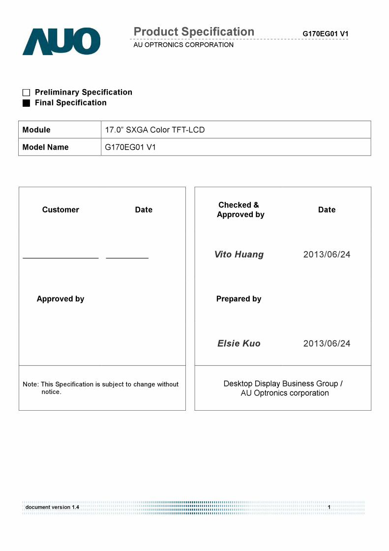
AU OPTRONICS CORPORATION Product Specification
document version 1.4 1
G170EG01 V1
Preliminary Specification Final Specification
Module 17.0” SXGA Color TFT-LCD Model Name G170EG01 V1
Customer Date
Approved by
Note: This Specification is subject to change without notice.
Checked & Approved by Date
Vito Huang 2013/06/24
Prepared by
Elsie Kuo 2013/06/24
Desktop Display Business Group / AU Optronics corporation
AU OPTRONICS CORPORATION Product Specification
document version 1.4 2
G170EG01 V1
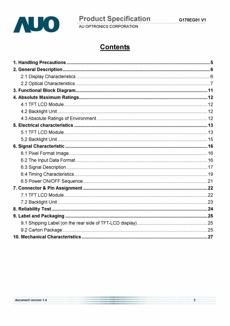
Contents
1. Handling Precautions ..................................................................................................................5 2. General Description.....................................................................................................................6
2.1 Display Characteristics ..........................................................................................................6 2.2 Optical Characteristics ...........................................................................................................7
3. Functional Block Diagram.........................................................................................................11 4. Absolute Maximum Ratings......................................................................................................12
4.1 TFT LCD Module..................................................................................................................12 4.2 Backlight Unit .......................................................................................................................12 4.3 Absolute Ratings of Environment ........................................................................................12
5. Electrical characteristics ..........................................................................................................13 5.1 TFT LCD Module..................................................................................................................13 5.2 Backlight Unit .......................................................................................................................15
6. Signal Characteristic .................................................................................................................16 6.1 Pixel Format Image..............................................................................................................16 6.2 The Input Data Format.........................................................................................................16 6.3 Signal Description ................................................................................................................17 6.4 Timing Characteristics..........................................................................................................19 6.5 Power ON/OFF Sequence...................................................................................................21
7. Connector & Pin Assignment ...................................................................................................22 7.1 TFT LCD Module..................................................................................................................22 7.2 Backlight Unit .......................................................................................................................23
8. Reliability Test............................................................................................................................24 9. Label and Packaging .................................................................................................................25
9.1 Shipping Label (on the rear side of TFT-LCD display)........................................................25 9.2 Carton Package ...................................................................................................................25
10. Mechanical Characteristics ....................................................................................................27
AU OPTRONICS CORPORATION Product Specification
document version 1.4 3
G170EG01 V1
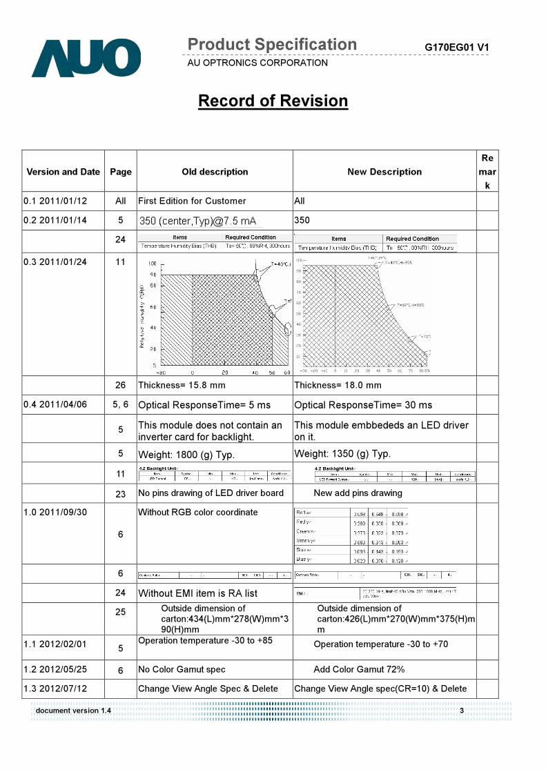
Record of Revision
Version and Date Page Old description New Description Remark
0.1 2011/01/12 All First Edition for Customer All 0.2 2011/01/14 5 350 24 0.3 2011/01/24 11
26 Thickness= 15.8 mm Thickness= 18.0 mm 0.4 2011/04/06 5, 6 Optical ResponseTime= 5 ms Optical ResponseTime= 30 ms 5 This module does not contain an
inverter card for backlight. This module embbededs an LED driver on it.
5 Weight: 1800 (g) Typ. Weight: 1350 (g) Typ. 11 23 No pins drawing of LED driver board New add pins drawing 1.0 2011/09/30
6 Without RGB color coordinate
6 24 Without EMI item is RA list 25 Outside dimension of carton:434(L)mm*278(W)mm*390(H)mm
Outside dimension of carton:426(L)mm*270(W)mm*375(H)mm 1.1 2012/02/01 5 Operation temperature -30 to +85
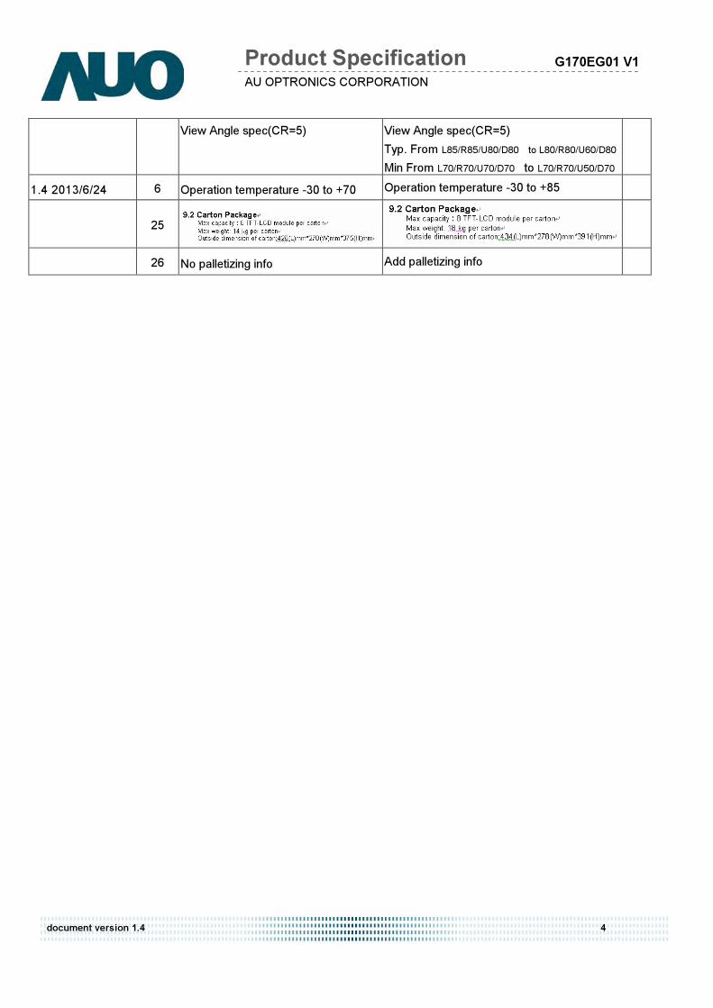
Operation temperature -30 to +70 1.2 2012/05/25 6 No Color Gamut spec Add Color Gamut 72% 1.3 2012/07/12 Change View Angle Spec & Delete Change View Angle spec(CR=10) & Delete
AU OPTRONICS CORPORATION Product Specification
document version 1.4 4
G170EG01 V1
View Angle spec(CR=5) View Angle spec(CR=5) Typ. From L85/R85/U80/D80 to L80/R80/U60/D80
Min From L70/R70/U70/D70 to L70/R70/U50/D70
1.4 2013/6/24 6 Operation temperature -30 to +70 Operation temperature -30 to +85
25
26 No palletizing info Add palletizing info
AU OPTRONICS CORPORATION Product Specification
document version 1.4 5
G170EG01 V1
1. Handling Precautions 1) Since front polarizer is easily damaged, pay attention not to scratch it. 2) Be sure to turn off power supply when inserting or disconnecting from input connector. 3) Wipe off water drop immediately. Long contact with water may cause discoloration or spots. 4) When the panel surface is soiled, wipe it with absorbent cotton or other soft cloth. 5) Since the panel is made of glass, it may break or crack if dropped or bumped on hard surface. 6) Since CMOS LSI is used in this module, take care of static electricity and insure human earth when
handling. 7) Do not open or modify the Module Assembly. 8) Do not press the reflector sheet at the back of the module to any directions. 9) In case if a Module has to be put back into the packing container slot after once it was taken out
from the container, do not press the center of the LED light bar edge. Instead, press at the far ends of the LED light bar edge softly. Otherwise the TFT Module may be damaged.
10) At the insertion or removal of the Signal Interface Connector, be sure not to rotate nor tilt the Interface Connector of the TFT Module.
11) After installation of the TFT Module into an enclosure, do not twist nor bend the TFT Module even momentary. At designing the enclosure, it should be taken into consideration that no bending/twisting forces are applied to the TFT Module from outside. Otherwise the TFT Module may be damaged.
12) Small amount of materials having no flammability grade is used in the LCD module. The LCD module should be supplied by power complied with requirements of Limited Power Source (IEC60950 or UL1950), or be applied exemption.
AU OPTRONICS CORPORATION Product Specification
document version 1.4 6
G170EG01 V1
2. General Description This specification applies to the 17 inch Color TFT-LCD Module G170EG01 V1. The display supports the SXGA+ (1280(H) x 1024(V)) screen format and 16.7M colors (RGB 6-bits+Hi-FRC data).All input signals are 2 Channel LVDS interface compatible. This module embbededs an LED driver on it. 2.1 Display Characteristics The following items are characteristics summary on the table under 25 condition:
Items Unit Specifications Screen Diagonal [mm] 432 (17.0”) Active Area [mm] 337.920(H) × 270.336(V) Pixels H x V 1280 × 3(RGB) × 1024 Pixel Pitch [mm] 0.264(per one triad) × 0.264 Pixel Arrangement R.G.B. Vertical Stripe Display Mode Normally White White Luminance [cd/m2] 350 Contrast Ratio 800 : 1 (Typ) Optical ResponseTime [msec] 30 (Typ) Nominal Input Voltage VDD [Volt] +5.0 (Typ) Power Consumption (VDD line + LED line) [Watt] 22 W (Typ.)
(with LED driver, all black pattern) Weight [Grams] 1350 Typ. Physical Size (H x V x D) [mm] 358.5(H) x 296.5(V) Typ. x 18.0(D) Max Electrical Interface Dual Channel LVDS Surface Treatment Anti-glare type, Hardness 3H Support Color 16.7M colors (RGB 6-bits +Hi-FRC data) Temperature Range Operating Storage (Non-Operating)
[oC] [oC]
-30 to +85 -30 to +85
RoHS Compliance RoHS Compliance
AU OPTRONICS CORPORATION Product Specification
document version 1.4 7
G170EG01 V1
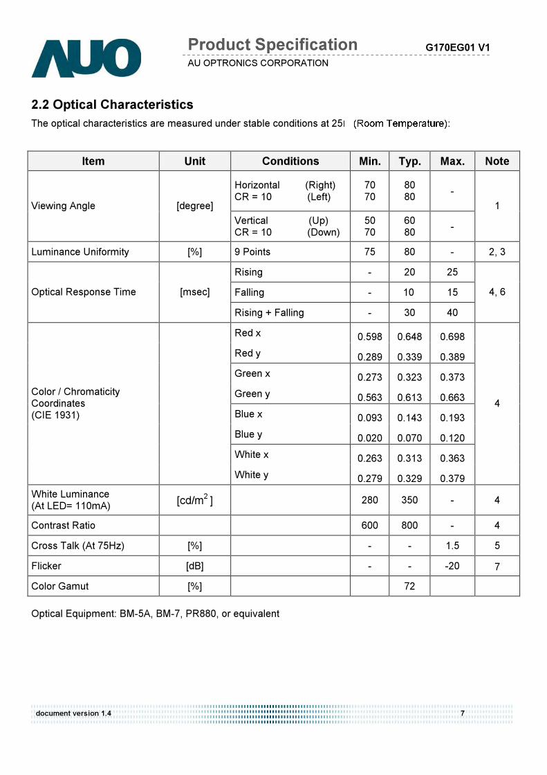
2.2 Optical Characteristics The optical characteristics are measured under stable conditions at 25(RoomTemperature):
Item Unit Conditions Min. Typ. Max. Note Horizontal (Right) CR = 10 (Left)
70 70
80 80 -
Viewing Angle [degree] Vertical (Up) CR = 10 (Down)
50 70
60 80 -
1
Luminance Uniformity [%] 9 Points 75 80 - 2, 3 Rising - 20 25 Falling - 10 15 Optical Response Time [msec] Rising + Falling - 30 40
4, 6
Red x 0.598 0.648 0.698 Red y 0.289 0.339 0.389 Green x 0.273 0.323 0.373 Green y 0.563 0.613 0.663 Blue x 0.093 0.143 0.193 Blue y 0.020 0.070 0.120 White x 0.263 0.313 0.363
Color / Chromaticity Coordinates (CIE 1931)
White y 0.279 0.329 0.379
4
White Luminance (At LED= 110mA) [cd/m2 ] 280 350 - 4
Contrast Ratio 600 800 - 4 Cross Talk (At 75Hz) [%] - - 1.5 5 Flicker [dB] - - -20 7 Color Gamut [%] 72
Optical Equipment: BM-5A, BM-7, PR880, or equivalent
AU OPTRONICS CORPORATION Product Specification
document version 1.4 8
G170EG01 V1
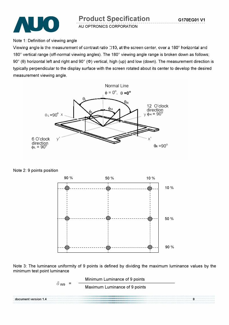
Note 1: Definition of viewing angle Viewingangleisthemeasurementofcontrastratio10,atthescreencenter,overa180°horizontaland180° vertical range (off-normal viewing angles). The 180° viewing angle range is broken down as follows; 90° (θ) horizontal left and right and 90° (Φ) vertical, high (up) and low (down). The measurement direction is typically perpendicular to the display surface with the screen rotated about its center to develop the desired measurement viewing angle.
Note 2: 9 points position Note 3: The luminance uniformity of 9 points is defined by dividing the maximum luminance values by the minimum test point luminance Minimum Luminance of 9 points δW9 = Maximum Luminance of 9 points
50 %
90 %
90 % 50 % 10 %
10 %
AU OPTRONICS CORPORATION Product Specification
document version 1.4 9
G170EG01 V1
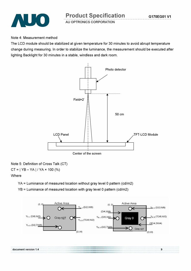
Note 4: Measurement method The LCD module should be stabilized at given temperature for 30 minutes to avoid abrupt temperature change during measuring. In order to stabilize the luminance, the measurement should be executed after lighting Backlight for 30 minutes in a stable, windless and dark room.
Note 5: Definition of Cross Talk (CT) CT = | YB – YA | / YA × 100 (%) Where
YA = Luminance of measured location without gray level 0 pattern (cd/m2) YB = Luminance of measured location with gray level 0 pattern (cd/m2)
Center of the screen
TFT-LCD Module
50 cm
Photo detector
LCD Panel
Field=2°
AU OPTRONICS CORPORATION Product Specification
document version 1.4 10
G170EG01 V1
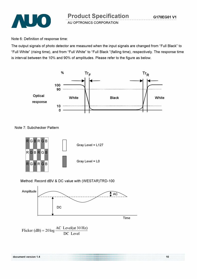
Note 6: Definition of response time: The output signals of photo detector are measured when the input signals are changed from “Full Black” to “Full White” (rising time), and from “Full White” to “Full Black ”(falling time), respectively. The response time is interval between the 10% and 90% of amplitudes. Please refer to the figure as below.
Note 7: Subchecker Pattern
R G B R G B
R G B R G B
R G B R G B
Method: Record dBV & DC value with (WESTAR)TRD-100 Level DC
Hz) 30Level(at AClog20(dB)Flicker =
100 90
10 0
%
Optical response
White Black White
Tr F Tr R
100 90
10 0
%
Optical response
White Black White
Tr F Tr R
Gray Level = L127
Gray Level = L0
Amplitude
Time
DC
AC
AU OPTRONICS CORPORATION Product Specification
document version 1.4 11
G170EG01 V1
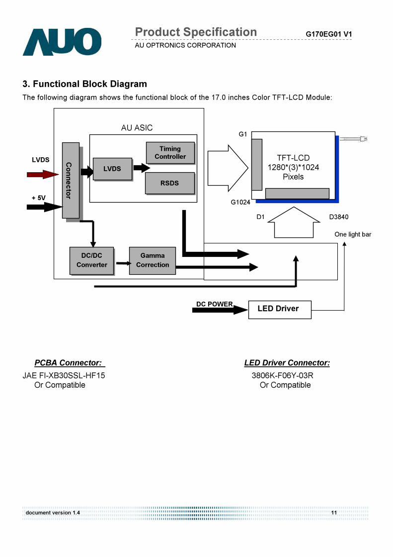
3. Functional Block Diagram The following diagram shows the functional block of the 17.0 inches Color TFT-LCD Module:
PCBA Connector: LED Driver Connector: JAE FI-XB30SSL-HF15 3806K-F06Y-03R
Or Compatible Or Compatible
One light bar
Connector
DC/DC Converter
LVDS Receiver
Timing Controller
Gamma Correction
TFT-LCD 1280*(3)*1024
Pixels
Y-Driver IC G1
G1024 D1 D3840
LED Driver DC POWER
AU ASIC
RSDS
LVDS
+ 5V
AU OPTRONICS CORPORATION Product Specification
document version 1.4 12
G170EG01 V1
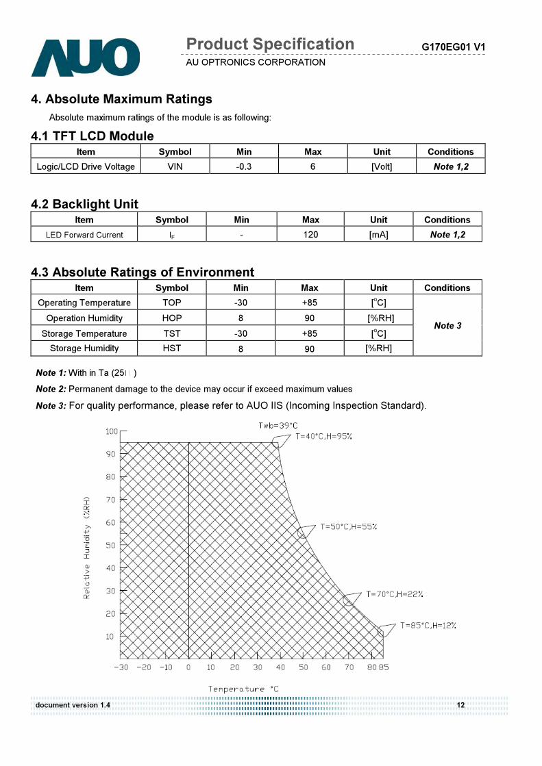
4. Absolute Maximum Ratings Absolute maximum ratings of the module is as following:
4.1 TFT LCD Module Item Symbol Min Max Unit Conditions
Logic/LCD Drive Voltage VIN -0.3 6 [Volt] Note 1,2 4.2 Backlight Unit
Item Symbol Min Max Unit Conditions LED Forward Current IF - 120 [mA] Note 1,2
4.3 Absolute Ratings of Environment
Item Symbol Min Max Unit Conditions Operating Temperature TOP -30 +85 [oC]
Operation Humidity HOP 8 90 [%RH] Storage Temperature TST -30 +85 [oC]
Storage Humidity HST 8 90 [%RH] Note 3
Note 1: With in Ta (25( ) Note 2: Permanent damage to the device may occur if exceed maximum values Note 3: For quality performance, please refer to AUO IIS (Incoming Inspection Standard).
AU OPTRONICS CORPORATION Product Specification
document version 1.4 13
G170EG01 V1
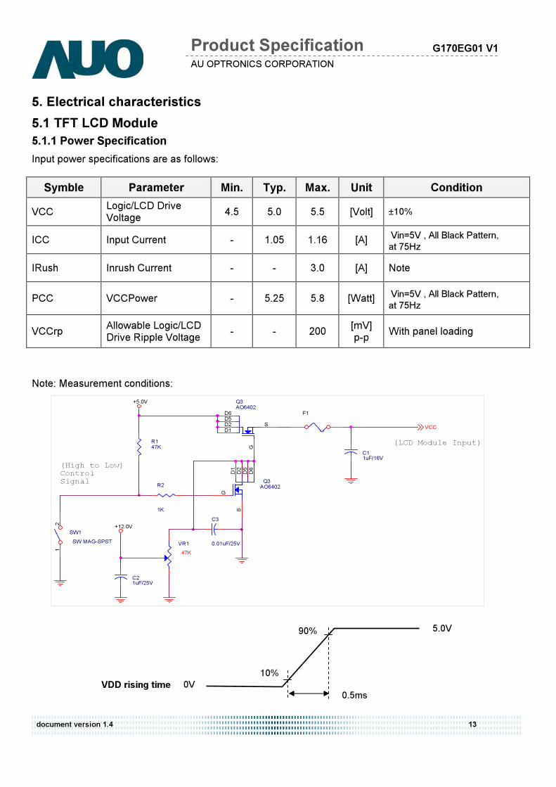
5. Electrical characteristics 5.1 TFT LCD Module 5.1.1 Power Specification Input power specifications are as follows:
Symble Parameter Min. Typ. Max. Unit Condition VCC Logic/LCD Drive
Voltage 4.5 5.0 5.5 [Volt] ±10% ICC Input Current - 1.05 1.16 [A] Vin=5V , All Black Pattern, at 75Hz IRush Inrush Current - - 3.0 [A] Note
PCC VCCPower - 5.25 5.8 [Watt] Vin=5V , All Black Pattern, at 75Hz VCCrp Allowable Logic/LCD
Drive Ripple Voltage - - 200 [mV] p-p With panel loading
Note: Measurement conditions:
+5.0V
+12.0V
VCC
R147K
R2
1K
VR147K
SW1SW MAG-SPST
12
F1
Q3AO6402
G
D2
SD1
D5
D6
C11uF/16V
Q3AO6402
G
D2 SD1
D5D6
C3
0.01uF/25V
C21uF/25V
(High to Low)ControlSignal
(LCD Module Input)
90%
10% VDD rising time 0V
5.0V
0.5ms
AU OPTRONICS CORPORATION Product Specification
document version 1.4 14
G170EG01 V1
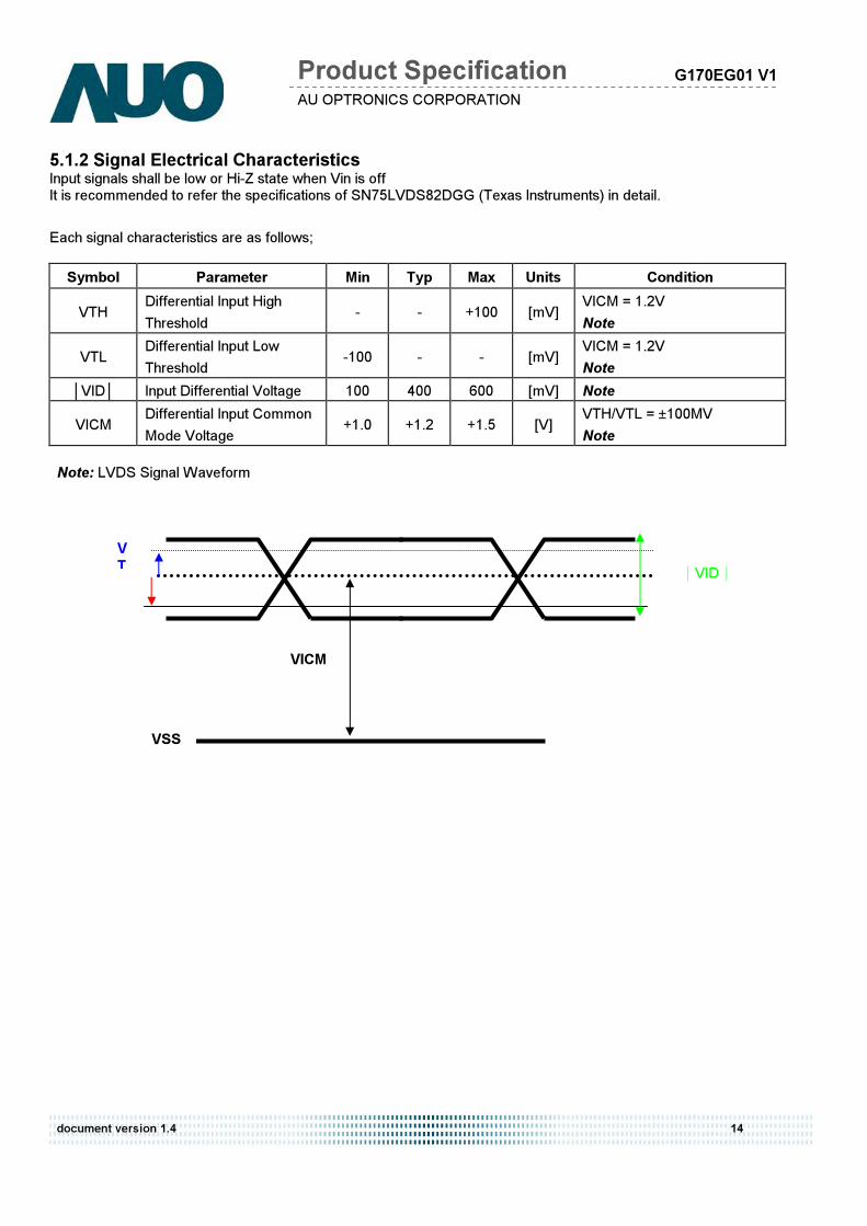
5.1.2 Signal Electrical Characteristics Input signals shall be low or Hi-Z state when Vin is off It is recommended to refer the specifications of SN75LVDS82DGG (Texas Instruments) in detail. Each signal characteristics are as follows;
Symbol Parameter Min Typ Max Units Condition VTH Differential Input High
Threshold - - +100 [mV] VICM = 1.2V Note
VTL Differential Input Low Threshold -100 - - [mV] VICM = 1.2V
Note VID Input Differential Voltage 100 400 600 [mV] Note
VICM Differential Input Common Mode Voltage +1.0 +1.2 +1.5 [V] VTH/VTL = ±100MV
Note Note: LVDS Signal Waveform
VTH VID
VICM
VSS
AU OPTRONICS CORPORATION Product Specification
document version 1.4 15
G170EG01 V1
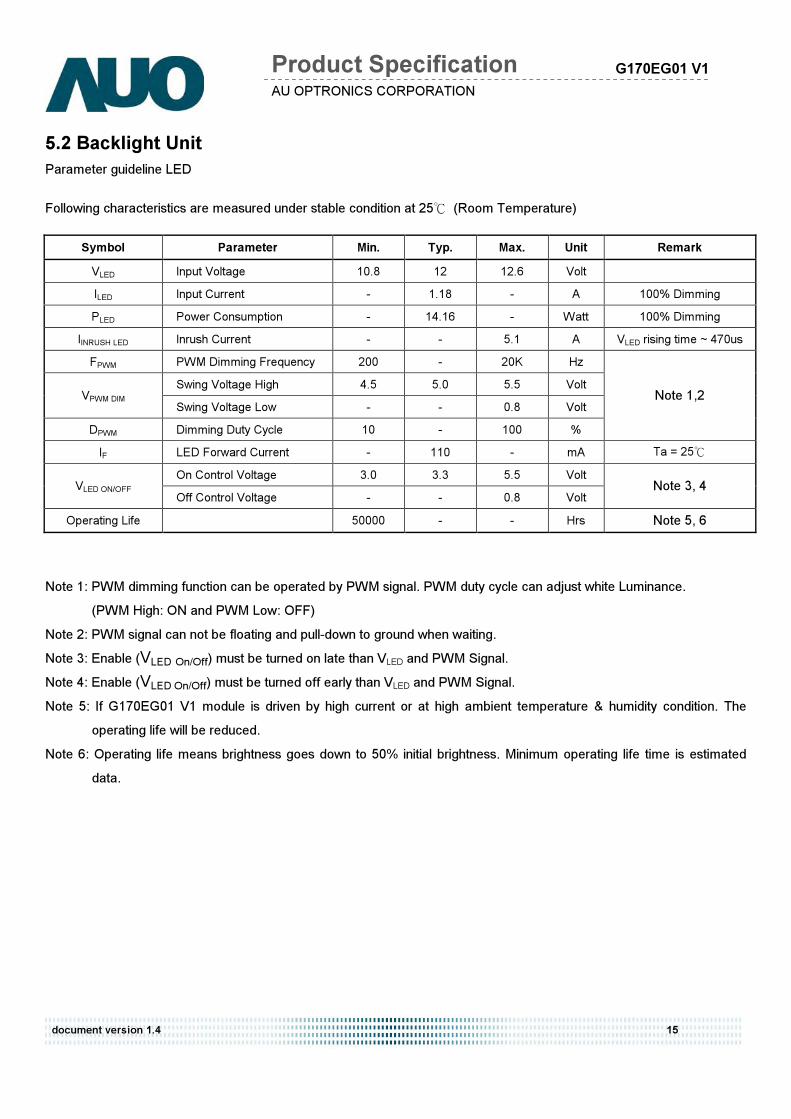
5.2 Backlight Unit Parameter guideline LED Following characteristics are measured under stable condition at 25 (Room Temperature)
Symbol Parameter Min. Typ. Max. Unit Remark VLED Input Voltage 10.8 12 12.6 Volt
ILED Input Current - 1.18 - A 100% Dimming PLED Power Consumption - 14.16 - Watt 100% Dimming
IINRUSH LED Inrush Current - - 5.1 A VLED rising time ~ 470us FPWM PWM Dimming Frequency 200 - 20K Hz
Swing Voltage High 4.5 5.0 5.5 Volt VPWM DIM Swing Voltage Low - - 0.8 Volt DPWM Dimming Duty Cycle 10 - 100 %
Note 1,2
IF LED Forward Current - 110 - mA Ta = 25 On Control Voltage 3.0 3.3 5.5 Volt VLED ON/OFF Off Control Voltage - - 0.8 Volt
Note 3, 4
Operating Life 50000 - - Hrs Note 5, 6 Note 1: PWM dimming function can be operated by PWM signal. PWM duty cycle can adjust white Luminance.
(PWM High: ON and PWM Low: OFF) Note 2: PWM signal can not be floating and pull-down to ground when waiting. Note 3: Enable (VLED On/Off) must be turned on late than VLED and PWM Signal. Note 4: Enable (VLED On/Off) must be turned off early than VLED and PWM Signal. Note 5: If G170EG01 V1 module is driven by high current or at high ambient temperature & humidity condition. The
operating life will be reduced. Note 6: Operating life means brightness goes down to 50% initial brightness. Minimum operating life time is estimated
data.
AU OPTRONICS CORPORATION Product Specification
document version 1.4 16
G170EG01 V1
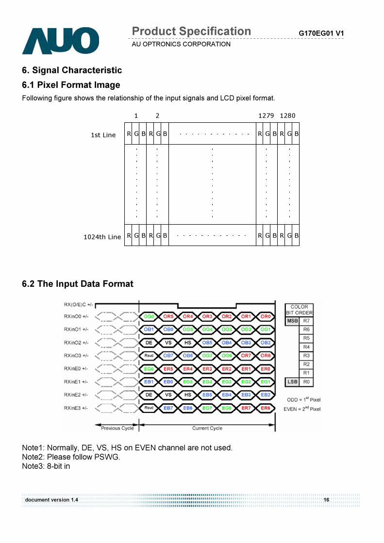
6. Signal Characteristic 6.1 Pixel Format Image Following figure shows the relationship of the input signals and LCD pixel format.
R G B R G B
R G B R G B
R G B R G B
R G B R G B
1 2 1279 1280
1st Line
1024th Line
6.2 The Input Data Format
Note1: Normally, DE, VS, HS on EVEN channel are not used. Note2: Please follow PSWG. Note3: 8-bit in
AU OPTRONICS CORPORATION Product Specification
document version 1.4 17
G170EG01 V1
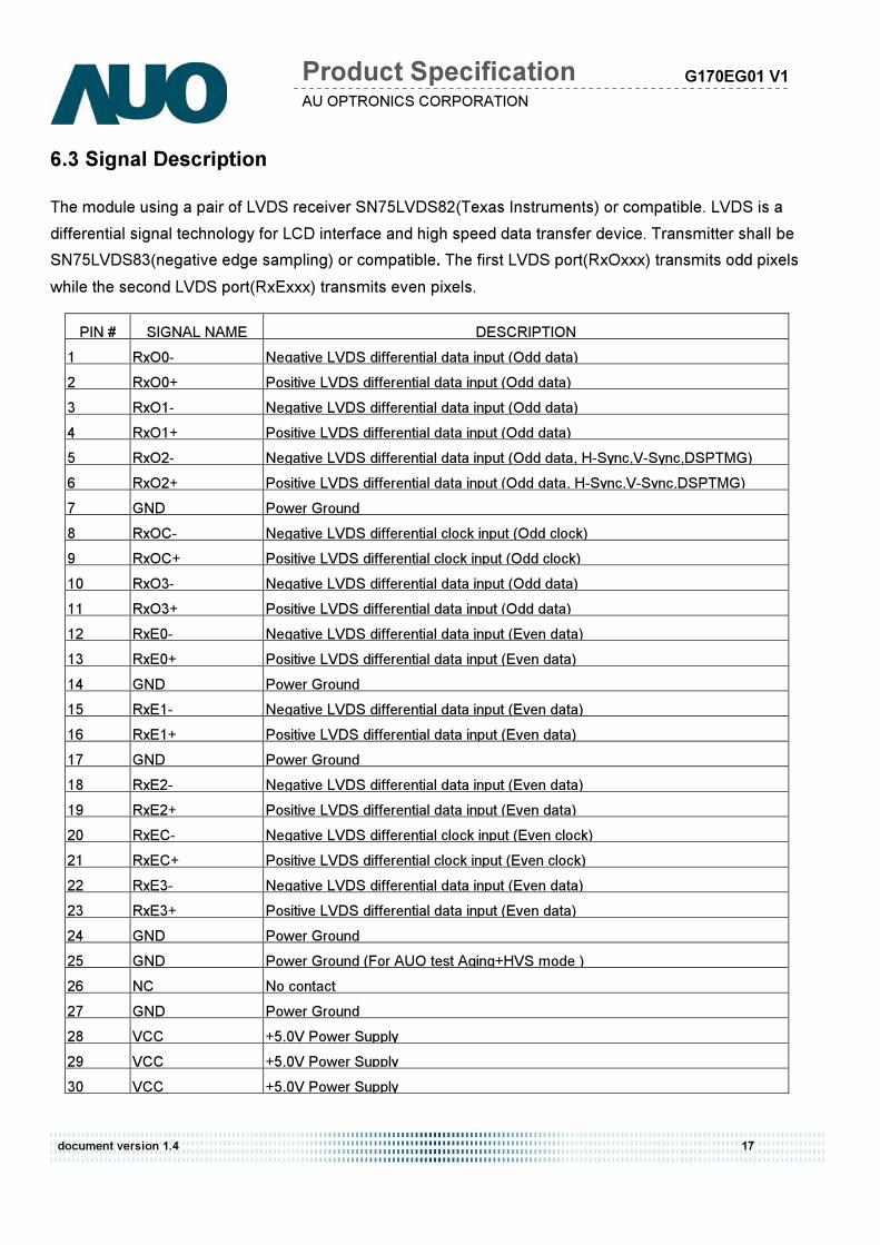
6.3 Signal Description The module using a pair of LVDS receiver SN75LVDS82(Texas Instruments) or compatible. LVDS is a differential signal technology for LCD interface and high speed data transfer device. Transmitter shall be SN75LVDS83(negative edge sampling) or compatible. The first LVDS port(RxOxxx) transmits odd pixels while the second LVDS port(RxExxx) transmits even pixels.
PIN # SIGNAL NAME DESCRIPTION 1 RxO0- Negative LVDS differential data input (Odd data) 2 RxO0+ Positive LVDS differential data input (Odd data) 3 RxO1- Negative LVDS differential data input (Odd data) 4 RxO1+ Positive LVDS differential data input (Odd data) 5 RxO2- Negative LVDS differential data input (Odd data, H-Sync,V-Sync,DSPTMG) 6 RxO2+ Positive LVDS differential data input (Odd data, H-Sync,V-Sync,DSPTMG) 7 GND Power Ground 8 RxOC- Negative LVDS differential clock input (Odd clock) 9 RxOC+ Positive LVDS differential clock input (Odd clock) 10 RxO3- Negative LVDS differential data input (Odd data) 11 RxO3+ Positive LVDS differential data input (Odd data) 12 RxE0- Negative LVDS differential data input (Even data) 13 RxE0+ Positive LVDS differential data input (Even data) 14 GND Power Ground 15 RxE1- Negative LVDS differential data input (Even data) 16 RxE1+ Positive LVDS differential data input (Even data) 17 GND Power Ground 18 RxE2- Negative LVDS differential data input (Even data) 19 RxE2+ Positive LVDS differential data input (Even data) 20 RxEC- Negative LVDS differential clock input (Even clock) 21 RxEC+ Positive LVDS differential clock input (Even clock) 22 RxE3- Negative LVDS differential data input (Even data) 23 RxE3+ Positive LVDS differential data input (Even data) 24 GND Power Ground 25 GND Power Ground (For AUO test Aging+HVS mode ) 26 NC No contact 27 GND Power Ground 28 VCC +5.0V Power Supply 29 VCC +5.0V Power Supply 30 VCC +5.0V Power Supply
AU OPTRONICS CORPORATION Product Specification
document version 1.4 18
G170EG01 V1
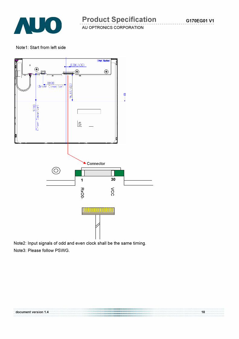
Note1: Start from left side
Note2: Input signals of odd and even clock shall be the same timing. Note3: Please follow PSWG.
Connector
1 30
RxO0-
VCC
AU OPTRONICS CORPORATION Product Specification
document version 1.4 19
G170EG01 V1
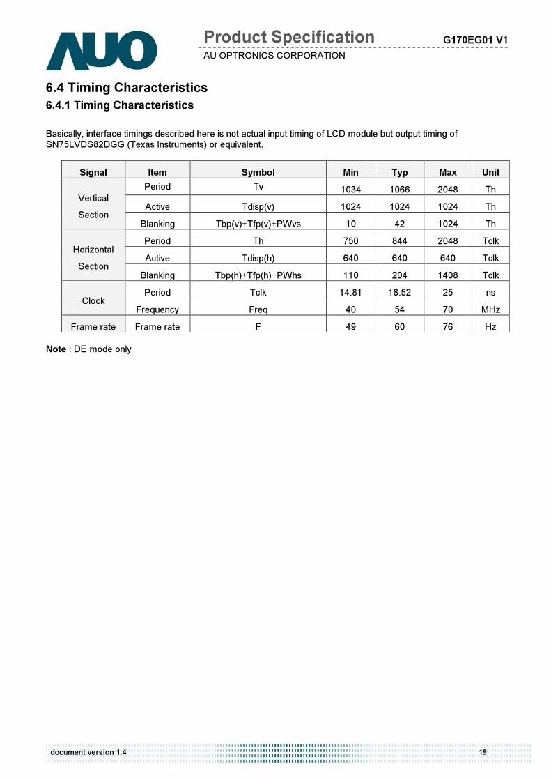
6.4 Timing Characteristics 6.4.1 Timing Characteristics Basically, interface timings described here is not actual input timing of LCD module but output timing of SN75LVDS82DGG (Texas Instruments) or equivalent.
Signal Item Symbol Min Typ Max Unit Period Tv 1034 1066 2048 Th Active Tdisp(v) 1024 1024 1024 Th Vertical
Section Blanking Tbp(v)+Tfp(v)+PWvs 10 42 1024 Th Period Th 750 844 2048 Tclk Active Tdisp(h) 640 640 640 Tclk Horizontal
Section Blanking Tbp(h)+Tfp(h)+PWhs 110 204 1408 Tclk Period Tclk 14.81 18.52 25 ns Clock Frequency Freq 40 54 70 MHz
Frame rate Frame rate F 49 60 76 Hz Note : DE mode only
AU OPTRONICS CORPORATION Product Specification
document version 1.4 20
G170EG01 V1
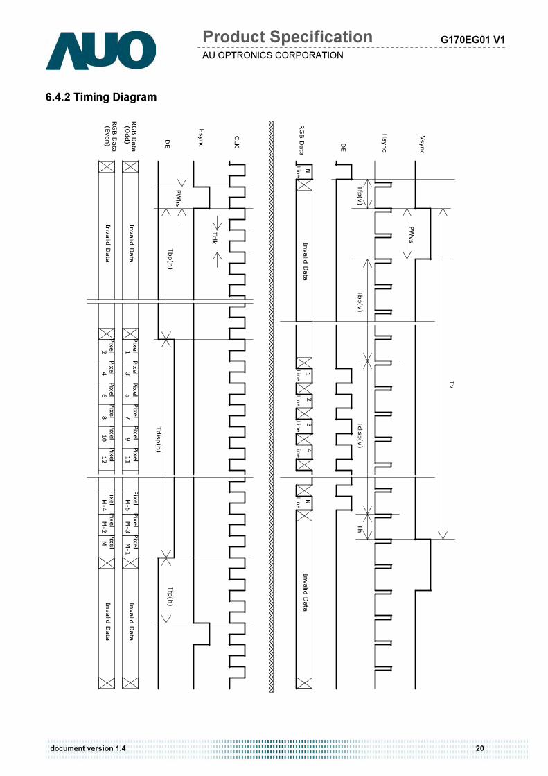
6.4.2 Timing Diagram
Hsync
Pixel
N1
M
Invalid Data
Tdisp(v)
10
DE
DE
Invalid Data
RGB Data
Th
2RGB Data (Even)
39
M-1
Invalid Data
1
N
Hsync
M-2
Invalid Data11
6 5M-3
Vsync
Invalid Data
CLK
M-5
Invalid Data
M-4
7
2
Tbp(h)
PixelPixel
PixelPixel
PixelRGB Data (Odd)
12
Tbp(v)
Tclk
PixelPixel
PixelPixel
PixelPixel
PixelPixel
PixelPixel
Pixel
Pixel8
43
4
Tv
Tdisp(h)
LineLine
LineLine
LineLine
Tfp(v)
Tfp(h)
PWvs
PWhs
AU OPTRONICS CORPORATION Product Specification
document version 1.4 21
G170EG01 V1
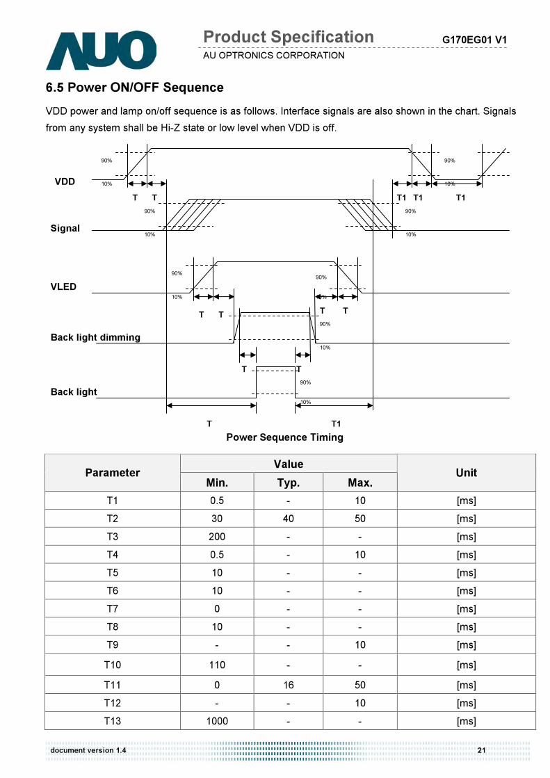
6.5 Power ON/OFF Sequence VDD power and lamp on/off sequence is as follows. Interface signals are also shown in the chart. Signals from any system shall be Hi-Z state or low level when VDD is off.
Power Sequence Timing
Value Parameter Min. Typ. Max. Unit
T1 0.5 - 10 [ms] T2 30 40 50 [ms] T3 200 - - [ms] T4 0.5 - 10 [ms] T5 10 - - [ms] T6 10 - - [ms] T7 0 - - [ms] T8 10 - - [ms] T9 - - 10 [ms] T10 110 - - [ms] T11 0 16 50 [ms] T12 - - 10 [ms] T13 1000 - - [ms]
90%
10%
90%
10%
10%
90%
90%
90%
90%
10%
10%
10%
T T
T
T T
T T
T1
T T
T1 T1 T1
VDD
Signal
VLED
Back light dimming
Back light
10%
10%
90%
90%
AU OPTRONICS CORPORATION Product Specification
document version 1.4 22
G170EG01 V1
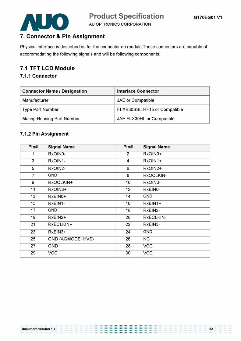
7. Connector & Pin Assignment Physical interface is described as for the connector on module.These connectors are capable of accommodating the following signals and will be following components. 7.1 TFT LCD Module 7.1.1 Connector Connector Name / Designation Interface Connector Manufacturer JAE or Compatible Type Part Number FI-XB30SSL-HF15 or Compatible Mating Housing Part Number JAE FI-X30HL or Compatible
7.1.2 Pin Assignment
Pin# Signal Name Pin# Signal Name 1 RxOIN0- 2 RxOIN0+ 3 RxOIN1- 4 RxOIN1+ 5 RxOIN2- 6 RxOIN2+ 7 GND 8 RxOCLKIN- 9 RxOCLKIN+ 10 RxOIN3- 11 RxOIN3+ 12 RxEIN0- 13 RxEIN0+ 14 GND 15 RxEIN1- 16 RxEIN1+ 17 GND 18 RxEIN2- 19 RxEIN2+ 20 RxECLKIN- 21 RxECLKIN+ 22 RxEIN3- 23 RxEIN3+ 24 GND 25 GND (AGMODE+HVS) 26 NC 27 GND 28 VCC 29 VCC 30 VCC
AU OPTRONICS CORPORATION Product Specification
document version 1.4 23
G170EG01 V1
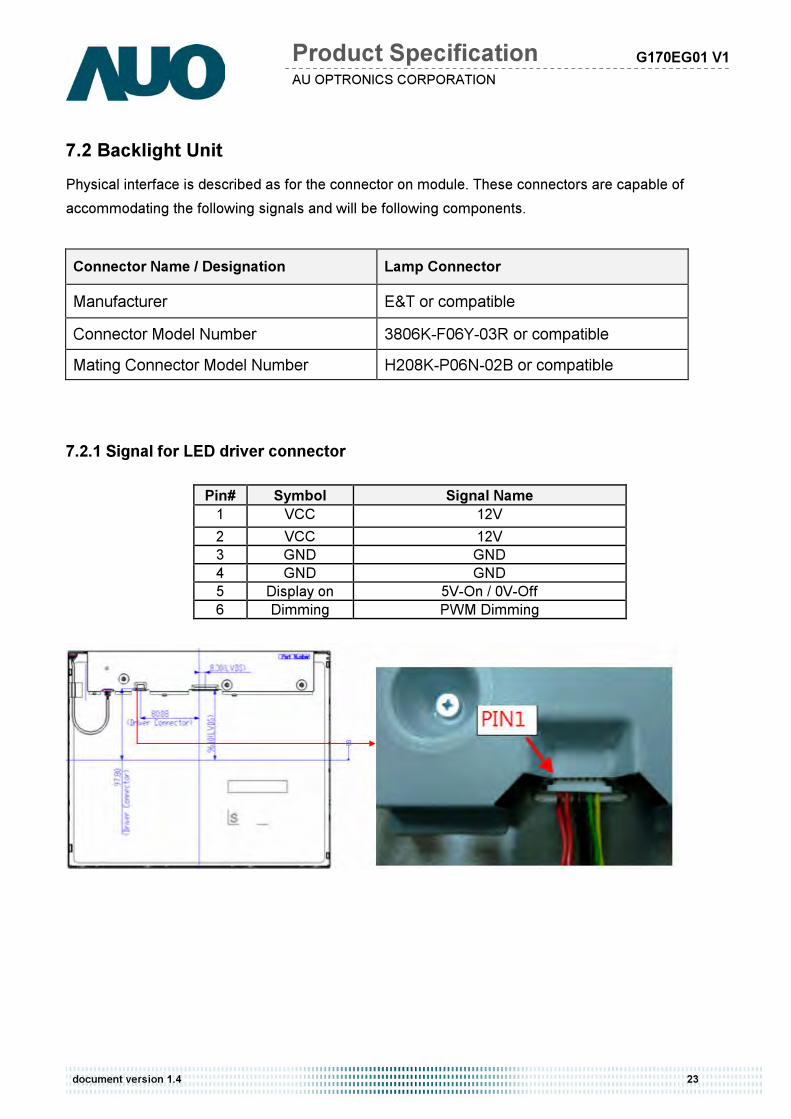
7.2 Backlight Unit Physical interface is described as for the connector on module. These connectors are capable of accommodating the following signals and will be following components. Connector Name / Designation Lamp Connector
Manufacturer E&T or compatible Connector Model Number 3806K-F06Y-03R or compatible Mating Connector Model Number H208K-P06N-02B or compatible
7.2.1 Signal for LED driver connector
Pin# Symbol Signal Name 1 VCC 12V 2 VCC 12V 3 GND GND 4 GND GND 5 Display on 5V-On / 0V-Off 6 Dimming PWM Dimming
AU OPTRONICS CORPORATION Product Specification
document version 1.4 24
G170EG01 V1
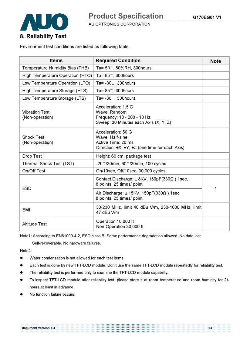
8. Reliability Test Environment test conditions are listed as following table.
Items Required Condition Note Temperature Humidity Bias (THB) Ta= 50*, 80%RH, 300hours High Temperature Operation (HTO) Ta= 85*, 300hours Low Temperature Operation (LTO) Ta= -30*,300hours High Temperature Storage (HTS) Ta= 85*,300hours Low Temperature Storage (LTS) Ta= -30*,300hours
Vibration Test (Non-operation)
Acceleration: 1.5 G Wave: Random Frequency: 10 - 200 - 10 Hz Sweep: 30 Minutes each Axis (X, Y, Z)
Shock Test (Non-operation)
Acceleration: 50 G Wave: Half-sine Active Time: 20 ms Direction: ±X, ±Y, ±Z (one time for each Axis)
Drop Test Height: 60 cm, package test Thermal Shock Test (TST) -20*/30min, 60*/30min, 100 cycles On/Off Test On/10sec, Off/10sec, 30,000 cycles
Contact Discharge: ± 8KV, 150pF(330Ω ) 1sec, 8 points, 25 times/ point.
ESD Air Discharge: ± 15KV, 150pF(330Ω ) 1sec 8 points, 25 times/ point.
1
EMI 30-230 MHz, limit 40 dBu V/m, 230-1000 MHz, limit 47 dBu V/m
Altitude Test Operation:10,000 ft Non-Operation:30,000 ft
Note1: According to EN61000-4-2, ESD class B: Some performance degradation allowed. No data lost Self-recoverable. No hardware failures.
Note2: Water condensation is not allowed for each test items. Each test is done by new TFT-LCD module. Don’t use the same TFT-LCD module repeatedly for reliability test. The reliability test is performed only to examine the TFT-LCD module capability. To inspect TFT-LCD module after reliability test, please store it at room temperature and room humidity for 24
hours at least in advance. No function failure occurs.
AU OPTRONICS CORPORATION Product Specification
document version 1.4 25
G170EG01 V1
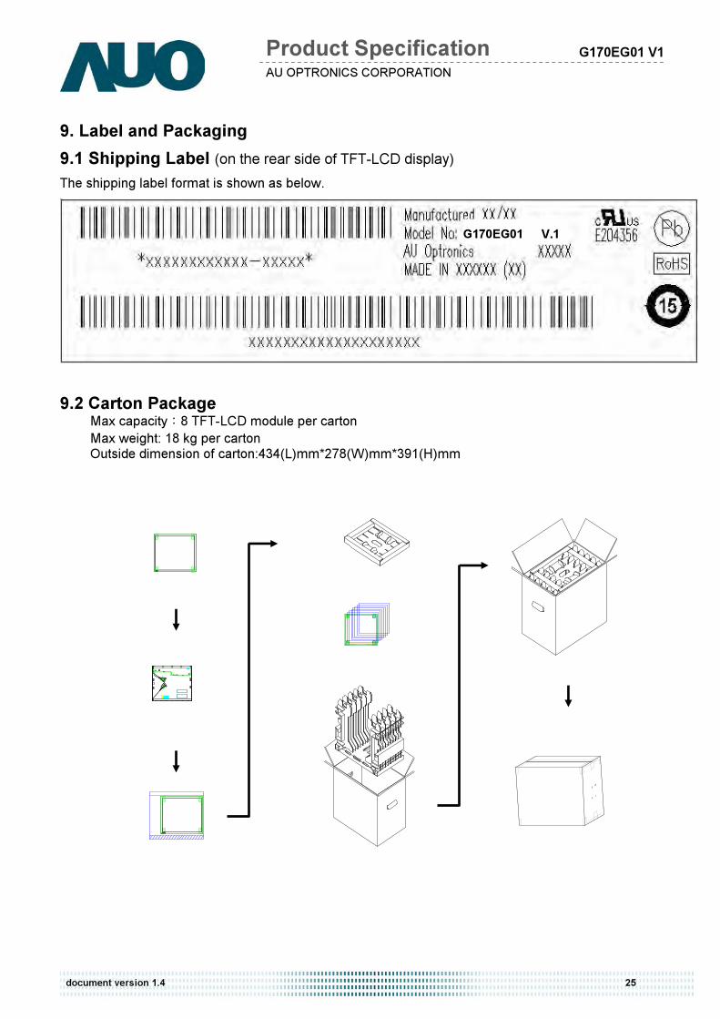
9. Label and Packaging 9.1 Shipping Label (on the rear side of TFT-LCD display) The shipping label format is shown as below.
9.2 Carton Package Max capacity:8 TFT-LCD module per carton Max weight: 18 kg per carton Outside dimension of carton:434(L)mm*278(W)mm*391(H)mm
G170EG01 V.1
AU OPTRONICS CORPORATION Product Specification
document version 1.4 26
G170EG01 V1
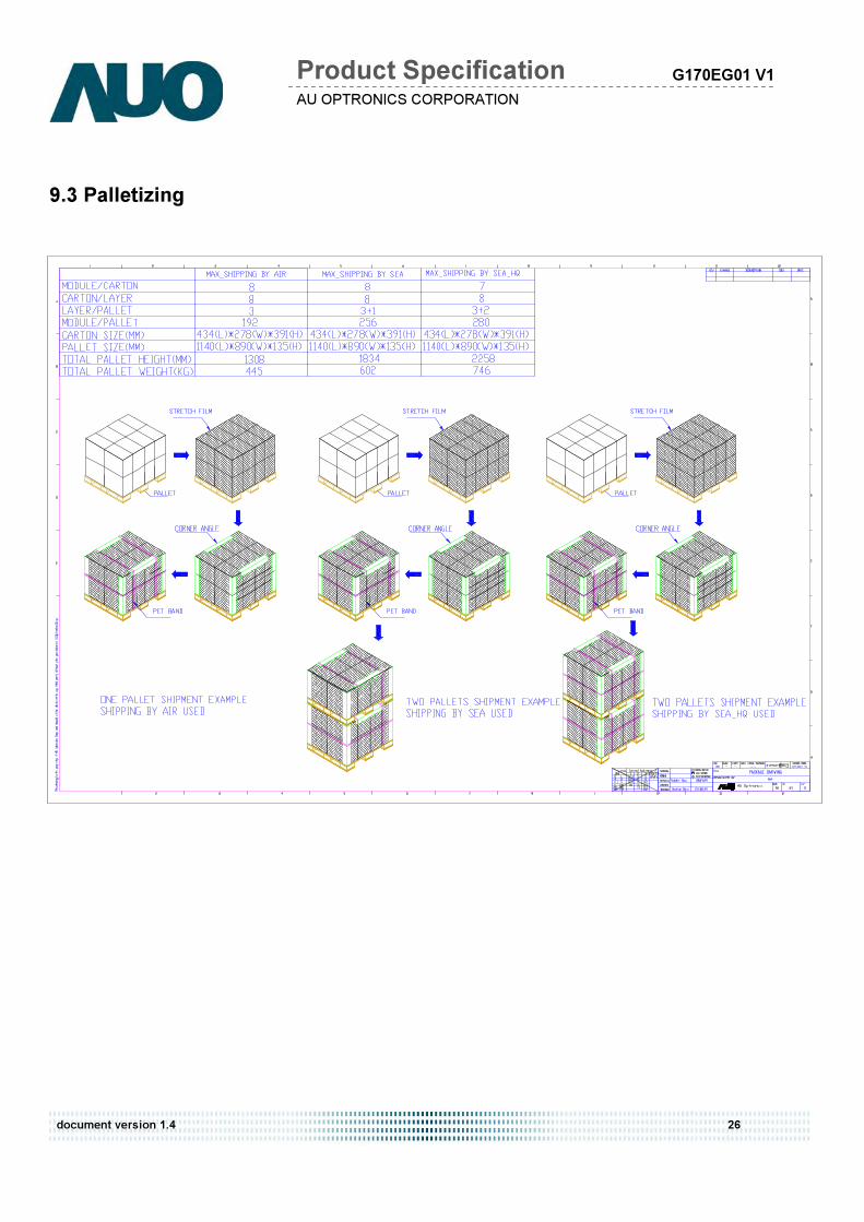
9.3 Palletizing
AU OPTRONICS CORPORATION Product Specification
document version 1.4 27
G170EG01 V1
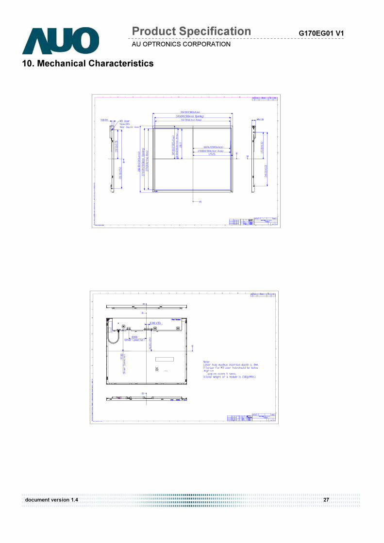
10. Mechanical Characteristics
1. General 1.1 This document is included the specifications of touch screen. 1.2 This touch screen is 5 wires analog resistive type. 1.3 It is designed to be activated by pressure of finger or stylus. 2. Environmental Specifications 2.1 Storing Environment Temperature Range:- 20 ~ 70 Humidity Range:20% RH ~ 90% RH (Non Condensing) 2.2 Operating Environment Temperature Range: -10 ~60 Humidity Range:20% RH ~80% RH (Non Condensing)
2.3 The above envionment is under normal pressure of the atmosphere.
3. Mechanical Specifications 3.1 Touch panel style style : Analog resistance 3.2 Dimension Specifications: Dimension outline 356.00 x 286.50 mm ± 0.30mm Viewable area 343.00 x 275.50 mm ± 0.20mm Active area 337.00 x 269.50 mm ± 0.20mm Total thickness 2.20 mm ± 0.20mm Tail length 205.00 mm ± 6.00mm 3.3 Operating Force ≦ 80g ( R0.8 Touch Pen)
3.4 Surface Hardness ≧ 3H (ASTM D3363, pressure 750g/45°) 3.5 Static Load : 5 kg within 10cm² area for 30sec 3.6 Impact : Impact at center area one time , no damage (25.0ψDIA. Steel
Ball/67g , Height=50cm)
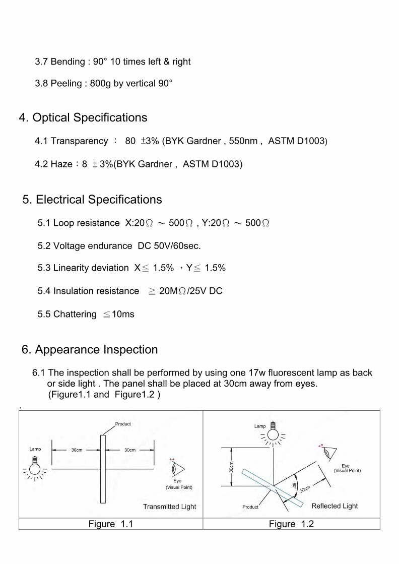
3.7 Bending : 90° 10 times left & right 3.8 Peeling : 800g by vertical 90° 4. Optical Specifications 4.1 Transparency : 80 ±3% (BYK Gardner , 550nm , ASTM D1003) 4.2 Haze:8 ± 3%(BYK Gardner , ASTM D1003) 5. Electrical Specifications 5.1 Loop resistance X:20Ω ~ 500Ω , Y:20Ω ~ 500Ω 5.2 Voltage endurance DC 50V/60sec. 5.3 Linearity deviation X≦ 1.5% ,Y≦ 1.5% 5.4 Insulation resistance ≧ 20MΩ/25V DC 5.5 Chattering ≦10ms 6. Appearance Inspection 6.1 The inspection shall be performed by using one 17w fluorescent lamp as back
or side light . The panel shall be placed at 30cm away from eyes. (Figure1.1 and Figure1.2 ) .
Figure 1.1 Figure 1.2
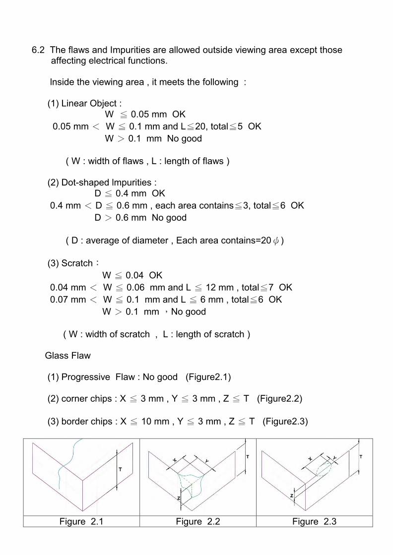
6.2 The flaws and Impurities are allowed outside viewing area except those
affecting electrical functions. lnside the viewing area , it meets the following : (1) Linear Object : W ≦ 0.05 mm OK 0.05 mm < W ≦ 0.1 mm and L≦20, total≦5 OK W > 0.1 mm No good ( W : width of flaws , L : length of flaws ) (2) Dot-shaped lmpurities : D ≦ 0.4 mm OK 0.4 mm < D ≦ 0.6 mm , each area contains≦3, total≦6 OK D > 0.6 mm No good ( D : average of diameter , Each area contains=20ψ) (3) Scratch: W ≦ 0.04 OK 0.04 mm < W ≦ 0.06 mm and L ≦ 12 mm , total≦7 OK 0.07 mm < W ≦ 0.1 mm and L ≦ 6 mm , total≦6 OK W > 0.1 mm ,No good ( W : width of scratch , L : length of scratch ) Glass Flaw (1) Progressive Flaw : No good (Figure2.1) (2) corner chips : X ≦ 3 mm , Y ≦ 3 mm , Z ≦ T (Figure2.2) (3) border chips : X ≦ 10 mm , Y ≦ 3 mm , Z ≦ T (Figure2.3)
Figure 2.1 Figure 2.2 Figure 2.3
X : Width direction against the edge line. Y : Length direction against the edge line. Z : Thickness direction against the edge line. The chips are not supposed to affect any of the electrical
functions. 7. Durability Knock test : 10,000,000 times keystrokes They still meet the specification required in section 5.1 and 5.4 , and section 5.3
satisfies X≦2.5%, Y≦2.5% ; Operating force must not exceed 250g after reliability test
8. Reliability 8.1 High temperature test After putting panels at 70 for 240 hours and allow panels stay in normal
environment for 4 hours , they still meet the specification required in section 5.1 and 5.4 , and section 5.3 satisfies X≦2.5%, Y≦2.5% ; Operating force must not exceed 250g after reliability test
8.2 Low temperature test After putting panels at -20 for 240 hours and allow panels stay in normal
environment for 4 hours , they still meet the specification required in section 5.1 and 5.4 , and section 5.3 satisfies X≦2.5%, Y≦2.5% ; Operating force must not exceed 250g after reliability test
8.3 High temperature and high humidity test After putting panels at 60 , 90% RH for 240 hours and allow panels stay in
normal environment for 4 hours , they still meet the specification required in section 5.1 and 5.4 , and section 5.3 satisfies X≦2.5%, Y≦2.5% ; Operating force must not exceed 250g after reliability test
8.4 Thermal shock test 1 Cycle : -20 →70 ( 60 minutes period ) After putting panels for 50 cycles and allow panels stay in normal environment
for 4 hours , they still meet the specification required in section 5.1 and 5.4 , and section 5.3 satisfies X≦2.5%, Y≦2.5% ; Operating force must not exceed 250g after reliability test
8.5 All the above tests may cause the film puffed .
9. Inspection Method 9.1 Linearity
(1) Short RT and RL(or short RL and LL). (2) apply voltage DC 5V. (3) short LT and LL (or short RT and LT). (4) apply grounding. (5) draw points along Lx and Ly at 5.0mm intervals within pattern area and
detect the voltage at SG. (6) measure the voltage differences between RT and LT(or RT and RL)
Figure 3.1 Figure 3.2 9.2 Specification
Linearity must meet the electrical characteristic specified in section 5.3 10. Warranty Miracletouch provide two years warranty of Miracletouch products. The followings are not in guaranty:
(1) Damages caused by improper handling from clients, including shipping, installation and integration.
(2) Damage caused by self-repairs, modifications or disassembling of the product. (3) Damages caused by disasters, either by natural causes or human factors, after
the delivery of products
11.Cautions 11.1 The bezel which contacts with PET film should keep a distance at least 3 mm from the active area to avoid short. 11.2 The bezel which contacts with PET film should not place heavy pressure on the film and the surface of bezel should be kept smooth. 11.3 Please keep clean on the surface of PET film , Don't attach any tape on that. 11.4 Neither pull tail upward nor push downward with an angle of 90° It should keep an arch at least R5. 11.5 If there exist any high voltage power , please make an adequate protect. 11.6 To avoid the high voltage static power to damage panel , please don't operate touch panel without connecting controller. 11.7 The panel could be cleaned with cloth containing ethanol or neutral cleaner. It is no effects to the characteristics 11.8 Miracletouch retain the right of changing the materials with same grade and specification.
Figure 4.1
DRAWING NO.
MODEL
APPROVED
DESIGN
DATE
REV
DATE
17" 5W
T
ouch P
anel
10170001
Eric
2012.11.25
01
2012.11.25
Eric
THIRD ANGLE
CAB-MB-MER4050UEBG-02
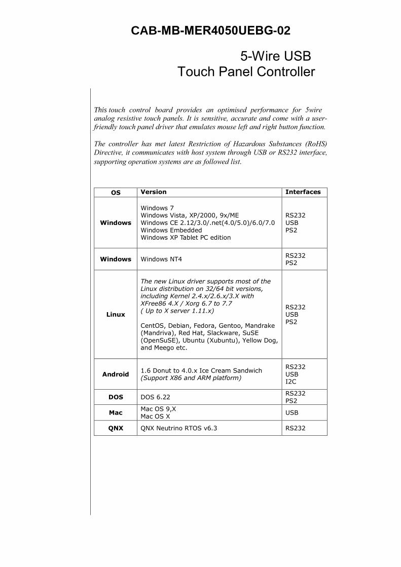
5-Wire USB Touch Panel Controller
This touch control board provides an optimised performance for 5wire analog resistive touch panels. It is sensitive, accurate and come with a user-friendly touch panel driver that emulates mouse left and right button function. The controller has met latest Restriction of Hazardous Substances (RoHS) Directive, it communicates with host system through USB or RS232 interface, supporting operation systems are as followed list.
OS Version Interfaces
Windows
Windows 7 Windows Vista, XP/2000, 9x/ME Windows CE 2.12/3.0/.net(4.0/5.0)/6.0/7.0 Windows Embedded Windows XP Tablet PC edition
RS232 USB PS2
Windows Windows NT4 RS232 PS2
Linux
The new Linux driver supports most of the Linux distribution on 32/64 bit versions, including Kernel 2.4.x/2.6.x/3.X with XFree86 4.X / Xorg 6.7 to 7.7 ( Up to X server 1.11.x) CentOS, Debian, Fedora, Gentoo, Mandrake (Mandriva), Red Hat, Slackware, SuSE (OpenSuSE), Ubuntu (Xubuntu), Yellow Dog, and Meego etc.
RS232 USB PS2
Android 1.6 Donut to 4.0.x Ice Cream Sandwich (Support X86 and ARM platform)
RS232 USB I2C
DOS DOS 6.22 RS232 PS2
Mac Mac OS 9,X Mac OS X USB
QNX QNX Neutrino RTOS v6.3 RS232
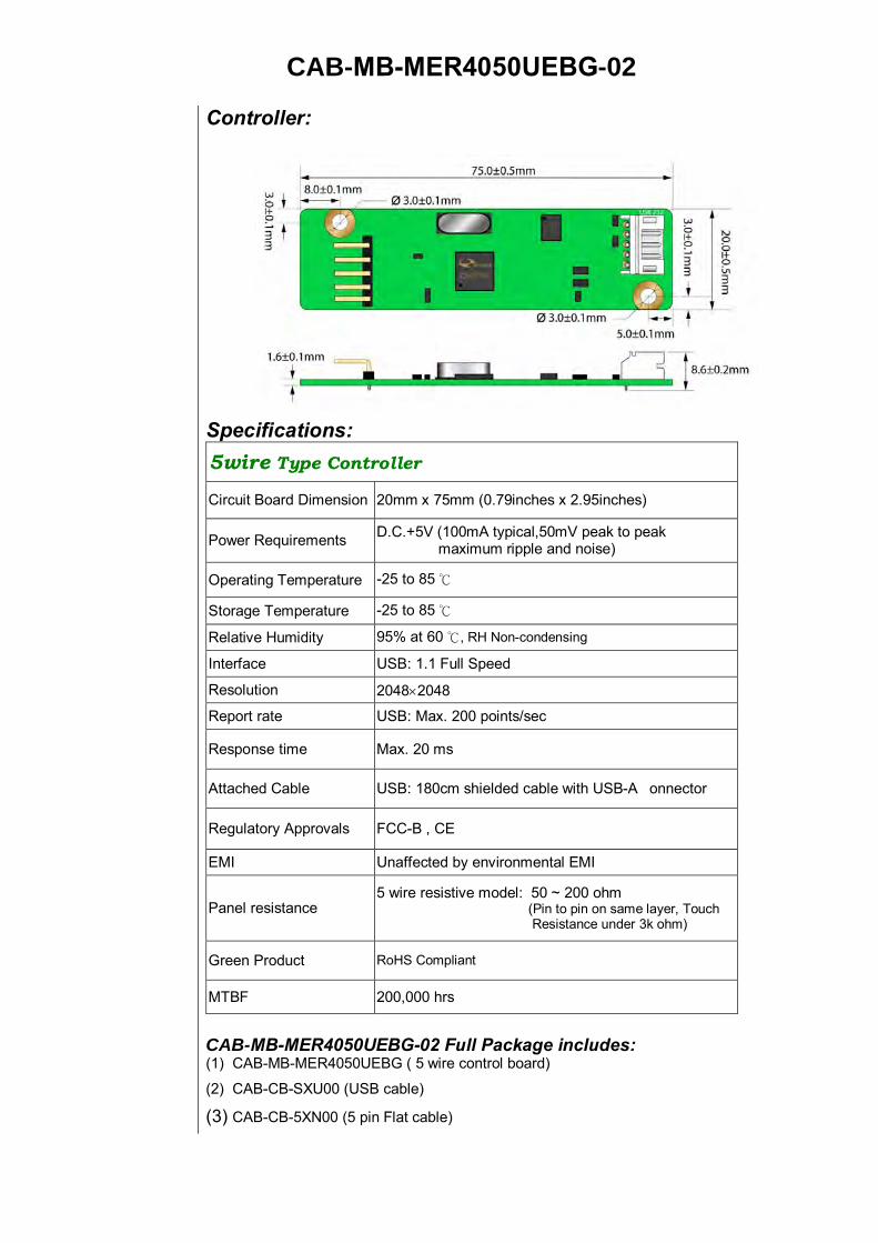
CAB-MB-MER4050UEBG-02
Controller: Specifications: 5wire Type Controller
Circuit Board Dimension 20mm x 75mm (0.79inches x 2.95inches)
Power Requirements D.C.+5V (100mA typical,50mV peak to peak maximum ripple and noise)
Operating Temperature -25 to 85
Storage Temperature -25 to 85
Relative Humidity 95% at 60 , RH Non-condensing
Interface USB: 1.1 Full Speed
Resolution 20482048
Report rate USB: Max. 200 points/sec
Response time Max. 20 ms
Attached Cable USB: 180cm shielded cable with USB-A onnector
Regulatory Approvals FCC-B , CE
EMI Unaffected by environmental EMI
Panel resistance 5 wire resistive model: 50 ~ 200 ohm (Pin to pin on same layer, Touch Resistance under 3k ohm)
Green Product RoHS Compliant
MTBF 200,000 hrs
CAB-MB-MER4050UEBG-02 Full Package includes: (1) CAB-MB-MER4050UEBG ( 5 wire control board)
(2) CAB-CB-SXU00 (USB cable)
(3) CAB-CB-5XN00 (5 pin Flat cable)
CAB-MB-MER4050UEBG-02
Rev V1.01
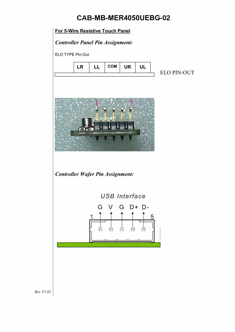
For 5-Wire Resistive Touch Panel Controller Panel Pin Assignment:
ELO TYPE Pin-Out
Controller Wafer Pin Assignment:
LR COM UL UR LL ELO PIN-OUT
1. General Description
1.1 Introduction
The CAB-F2281L is highly integrated TFT flat panel interface board that allows connect analog,
15 pin RGB source with TFT panels. From a single 12 V power supply, the CAB-F2281L generates
all the voltages required by the TFT panel and includes the power sequencing features. The
CAB-F2281L is capable of displaying FULL HD and lower resolutions. Synchronization signals of
applicable resolution modes can be detected automatically.
1.2 Technical Information Summary
Analog RGB Input port
Support up to 1920 X 1080
Support for Sync-on-Green (SOG)
DVI Compliant Digital Input
Single link on chip TMDS receiver
Long cable support to 1.65Ghz
Scaling
Support non-liner scaling from 4:3 to 16:9 or 16:9 to 4:3
Audio: 2W x 2
OSD key: Up to 7 KEY.
1.2 Power consumption
Panel: AU 19”
DC IN: 12V
Inverter: 4 Lamp
Resolution: 1280 X 1024 75Hz
Condition Audio minimum Audio maximum
A/D Board only 3W
A/D Board + Panel + Inverter 26W 28W
Power saving 0.4W
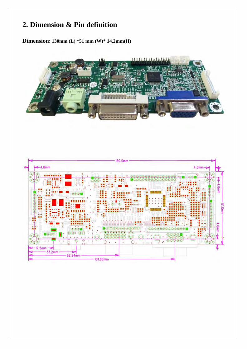
2. Dimension & Pin definition
Dimension: 130mm (L) *51 mm (W)* 14.2mm(H)
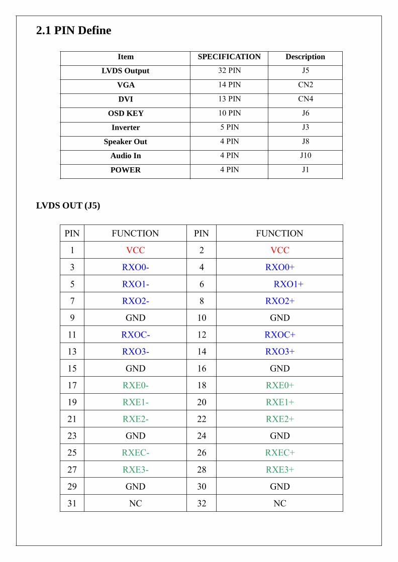
2.1 PIN Define
LVDS OUT (J5)
PIN FUNCTION PIN FUNCTION
1 VCC 2 VCC
3 RXO0- 4 RXO0+
5 RXO1- 6 RXO1+
7 RXO2- 8 RXO2+
9 GND 10 GND
11 RXOC- 12 RXOC+
13 RXO3- 14 RXO3+
15 GND 16 GND
17 RXE0- 18 RXE0+
19 RXE1- 20 RXE1+
21 RXE2- 22 RXE2+
23 GND 24 GND
25 RXEC- 26 RXEC+
27 RXE3- 28 RXE3+
29 GND 30 GND
31 NC 32 NC
Item SPECIFICATION Description
LVDS Output 32 PIN J5
VGA 14 PIN CN2
DVI 13 PIN CN4
OSD KEY 10 PIN J6
Inverter 5 PIN J3
Speaker Out 4 PIN J8
Audio In 4 PIN J10
POWER 4 PIN J1
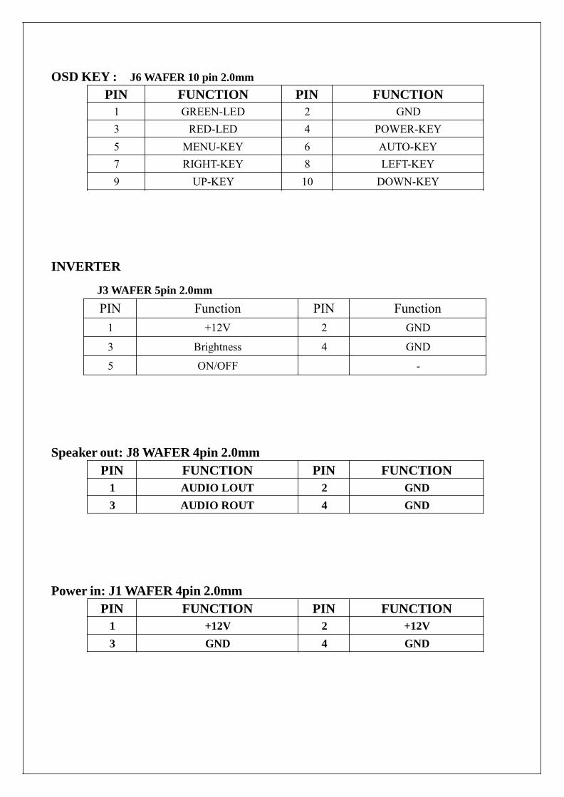
OSD KEY : J6 WAFER 10 pin 2.0mm
INVERTER
J3 WAFER 5pin 2.0mm
Speaker out: J8 WAFER 4pin 2.0mm
Power in: J1 WAFER 4pin 2.0mm
PIN FUNCTION PIN FUNCTION 1 +12V 2 +12V 3 GND 4 GND
PIN FUNCTION PIN FUNCTION 1 AUDIO LOUT 2 GND 3 AUDIO ROUT 4 GND
PIN Function PIN Function 1 +12V 2 GND
3 Brightness 4 GND
5 ON/OFF -
PIN FUNCTION PIN FUNCTION 1 GREEN-LED 2 GND 3 RED-LED 4 POWER-KEY 5 MENU-KEY 6 AUTO-KEY 7 RIGHT-KEY 8 LEFT-KEY 9 UP-KEY 10 DOWN-KEY
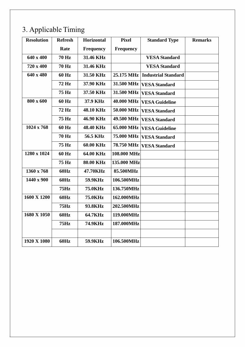
3. Applicable Timing
Resolution
Refresh
Rate
Horizontal
Frequency
Pixel
Frequency
Standard Type
Remarks
640 x 400 70 Hz 31.46 KHz VESA Standard
720 x 400 70 Hz 31.46 KHz VESA Standard
640 x 480
60 Hz 31.50 KHz 25.175 MHz Industrial Standard
72 Hz 37.90 KHz 31.500 MHz VESA Standard
75 Hz 37.50 KHz 31.500 MHz VESA Standard
800 x 600
60 Hz 37.9 KHz 40.000 MHz VESA Guideline
72 Hz 48.10 KHz 50.000 MHz VESA Standard
75 Hz 46.90 KHz 49.500 MHz VESA Standard
1024 x 768
60 Hz 48.40 KHz 65.000 MHz VESA Guideline
70 Hz 56.5 KHz 75.000 MHz VESA Standard
75 Hz 60.00 KHz 78.750 MHz VESA Standard
1280 x 1024
60 Hz 64.00 KHz 108.000 MHz
75 Hz 80.00 KHz 135.000 MHz
1360 x 768 60Hz 47.70KHz 85.500MHz
1440 x 900
60Hz 59.9KHz 106.500MHz
75Hz 75.0KHz 136.750MHz
1600 X 1200
60Hz 75.0KHz 162.000MHz
75Hz 93.8KHz 202.500MHz
1680 X 1050
60Hz 64.7KHz 119.000MHz
75Hz 74.9KHz 187.000MHz
1920 X 1080 60Hz 59.9KHz 106.500MHz
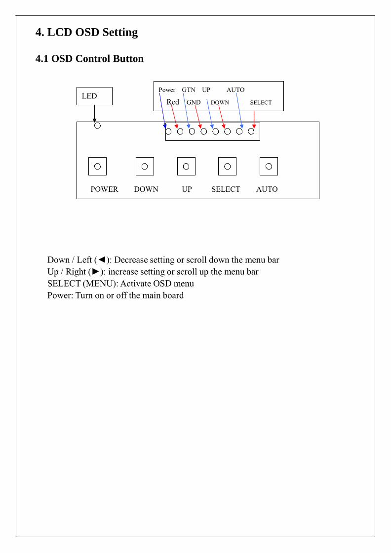
4. LCD OSD Setting
4.1 OSD Control Button
Down / Left (): Decrease setting or scroll down the menu bar Up / Right (): increase setting or scroll up the menu bar SELECT (MENU): Activate OSD menu Power: Turn on or off the main board
POWER DOWN UP SELECT AUTO
LED
Power GTN UP AUTO
Red GND DOWN SELECT
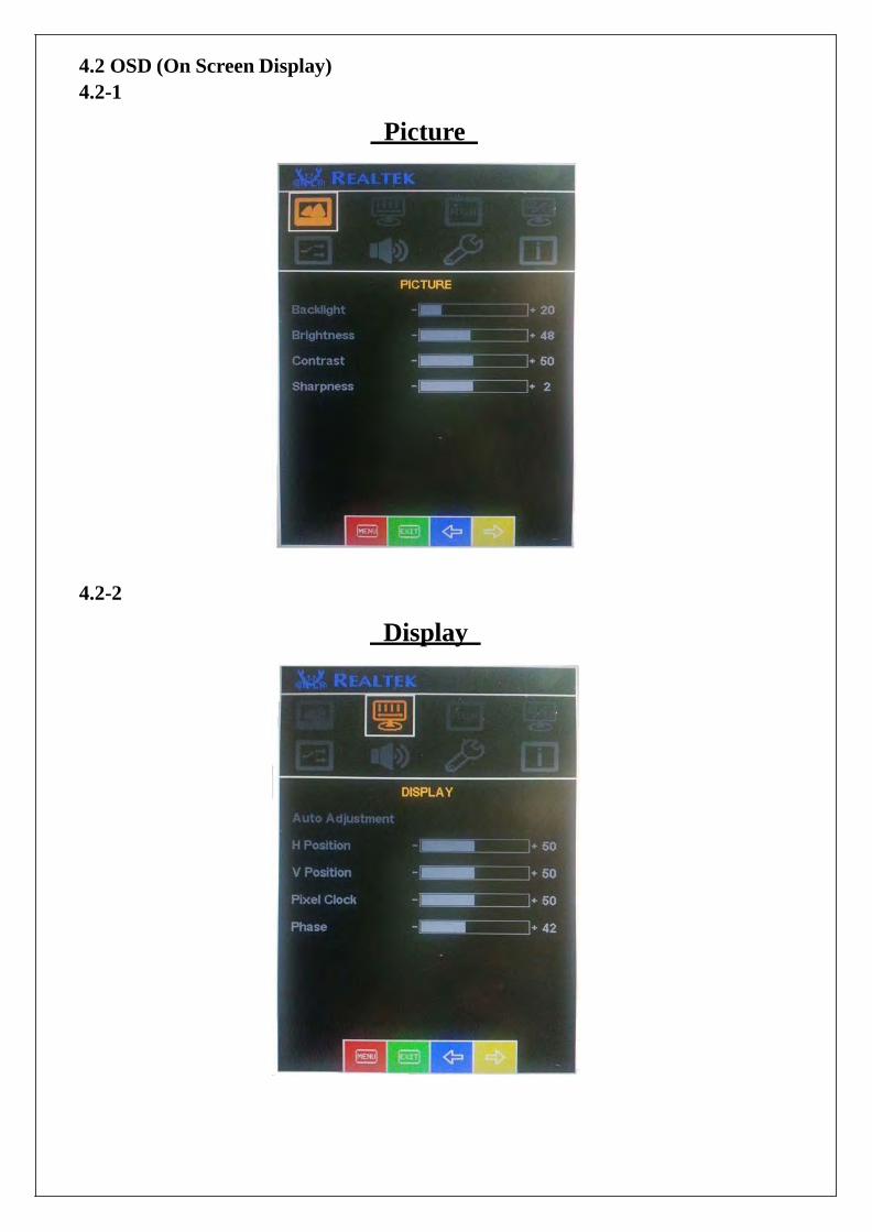
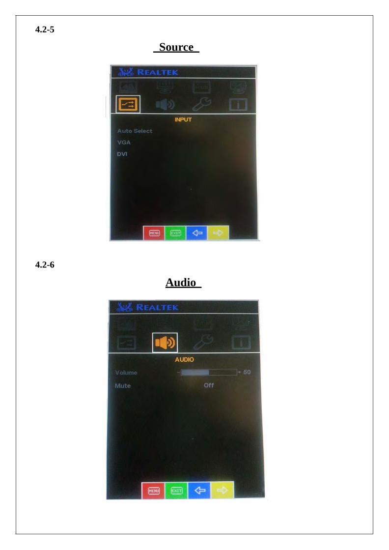
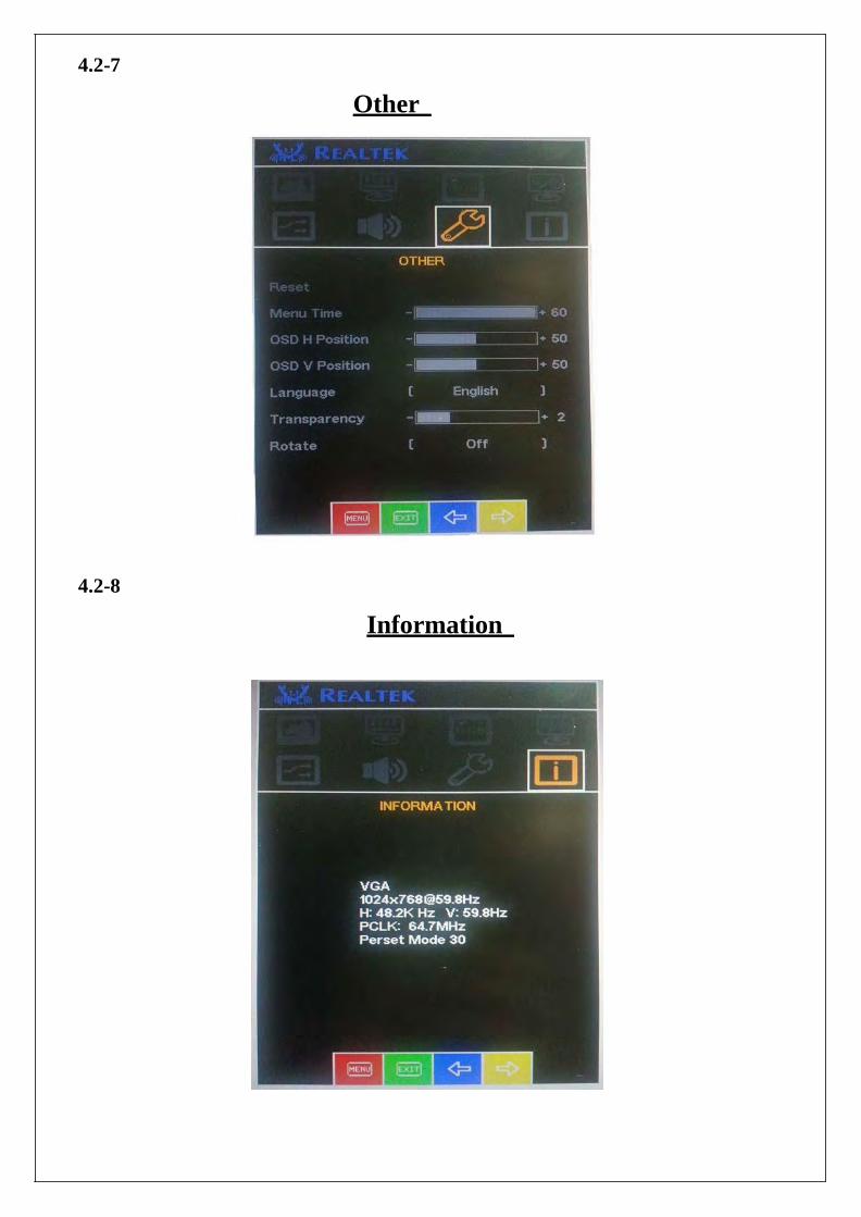
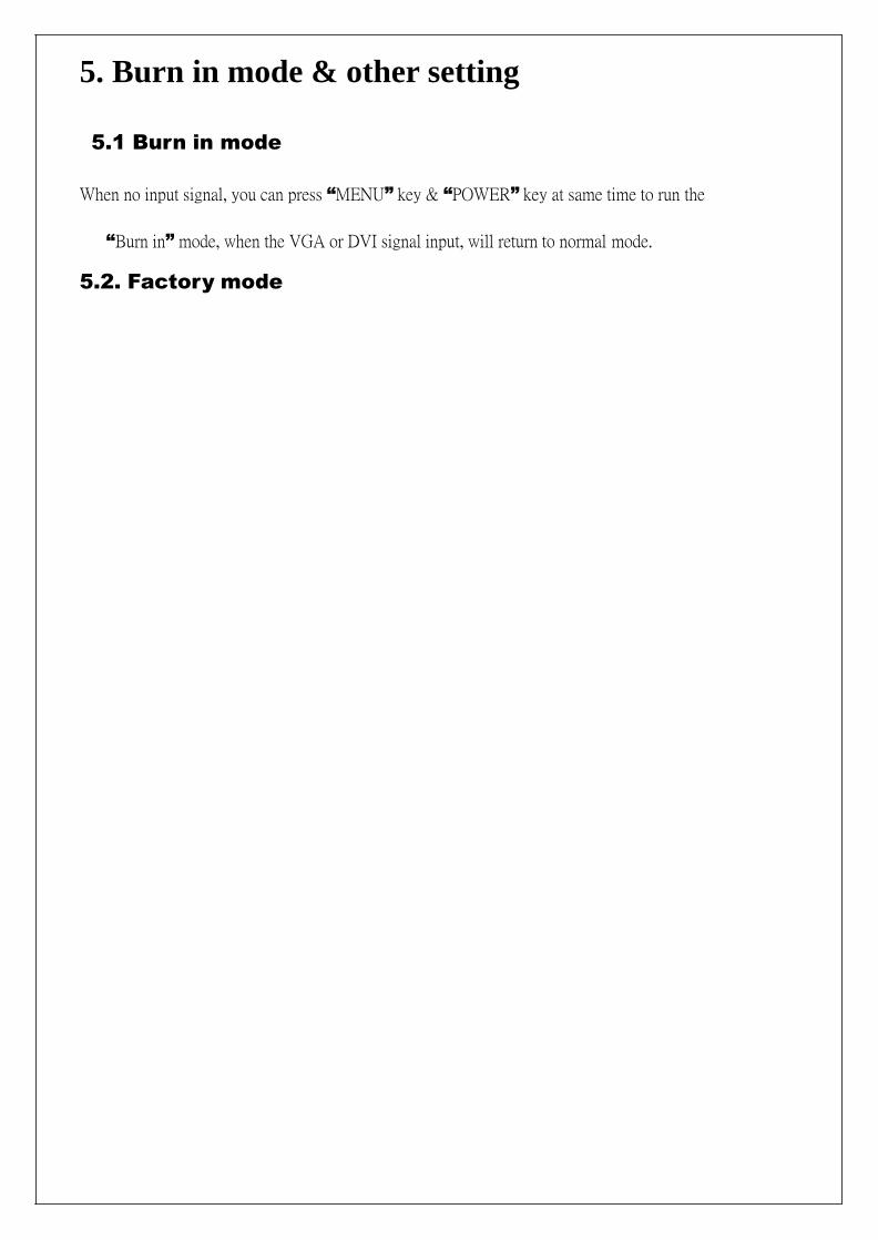
4.2 OSD (On Screen Display) 4.2-1
Picture
4.2-2
Display
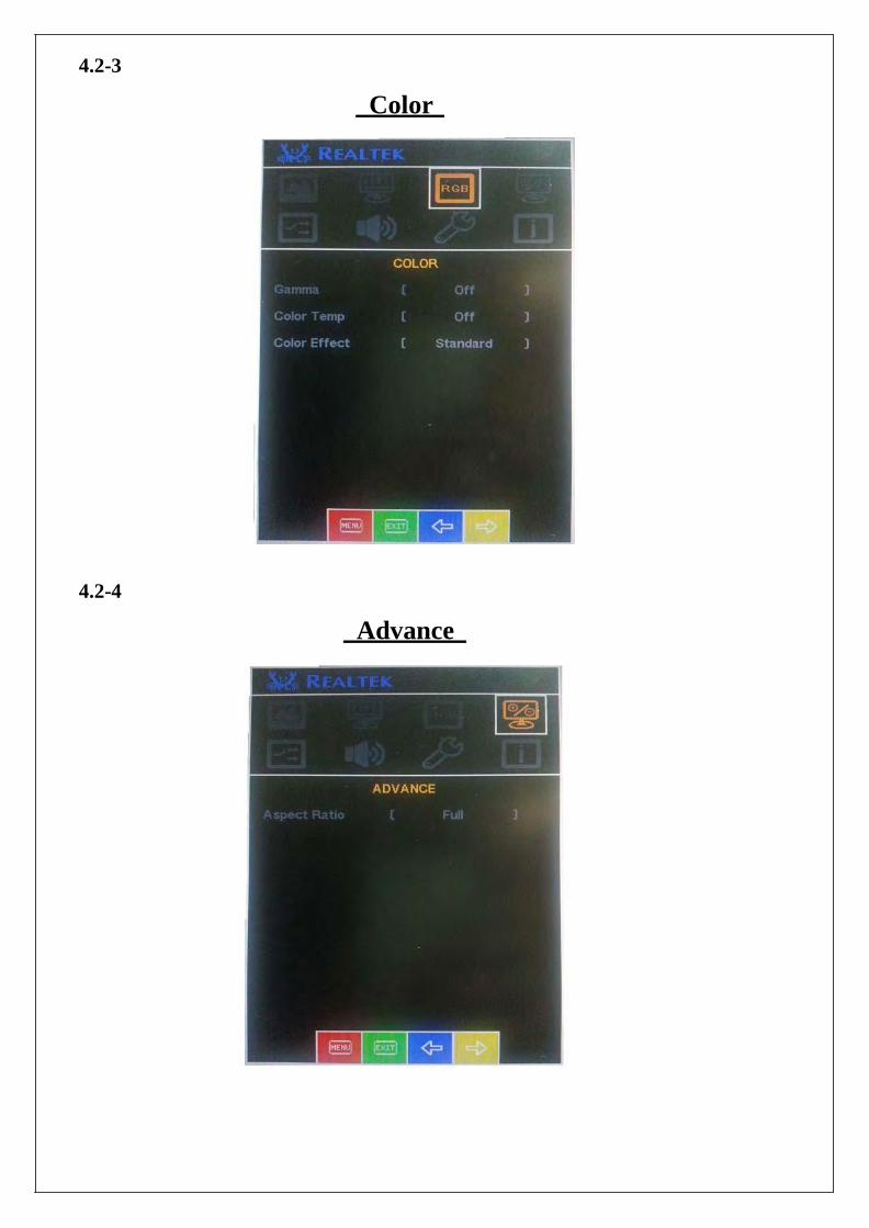
4.2-3
Color
4.2-4
Advance
4.2-5
Source
4.2-6
Audio
4.2-7
Other
4.2-8
Information
5. Burn in mode & other setting
5.1 Burn in mode
When no input signal, you can press “MENU” key & “POWER” key at same time to run the
“Burn in” mode, when the VGA or DVI signal input, will return to normal mode.
5.2. Factory mode