datasheet - renesas.com · 80c88 fn2949rev.5.00 page 5 of 39 sep 28, 2017 pin descriptions (minimum...
TRANSCRIPT
FN2949Rev.5.00
Sep 28, 2017
80C88CMOS 8-/16-Bit Microprocessor
DATASHEET
The Intersil 80C88 high performance 8-/16-bit CMOS CPU is manufactured using a self-aligned silicon gate CMOS process (Scaled SAJI IV). Two modes of operation, Minimum for small systems and Maximum for larger applications such as multiprocessing, allow user configuration to achieve the highest performance level.
Full TTL compatibility (with the exception of CLOCK) and industry-standard operation allow use of existing NMOS 8088 hardware and Intersil CMOS peripherals.
Complete software compatibility with the 80C86, 8086, and 8088 microprocessors allows use of existing software in new designs.
Related Literature• For a full list of related documents, visit our website
- 80C88 product page
Features• Compatible with NMOS 8088
• Direct software compatibility with 80C86, 8086, 8088
• 8-bit data bus interface; 16-bit internal architecture
• Completely static CMOS design
- DC . . . . . . . . . . . . . . . . . . . . . . . . . . . . . . . . . . 5MHz (80C88)
- DC . . . . . . . . . . . . . . . . . . . . . . . . . . . . . . . . 8MHz (80C88-2)
• Low power operation
- ICCSB. . . . . . . . . . . . . . . . . . . . . . . . . . . . . 500µA maximum
- ICCOP. . . . . . . . . . . . . . . . . . . . . . . . . 10mA/MHz maximum
• 1 MB of direct memory addressing capability
• 24 operand addressing modes
• Bit, byte, word, and block move operations
• 8-bit and 16-bit signed/unsigned arithmetic
• Bus-hold circuitry eliminates pull-up resistors
• Wide operating temperature ranges
- C80C88 . . . . . . . . . . . . . . . . . . . . . . . . . . . . . . .0°C to +70°C
- M80C88 . . . . . . . . . . . . . . . . . . . . . . . . . . . -55°C to +125°C
• Pb-free available (RoHS compliant)
Ordering Information
PART NUMBER(5MHz)
PARTMARKING
PART NUMBER(8MHz)
PARTMARKING
TEMPERATURERANGE
(°C) PACKAGE PKG. DWG. #
MD80C88/B MD80C88/B -55 to +125 40 LD CERDIP F40.6
CP80C88Z(Note)
CP80C88Z CP80C88-2Z 0 to +70 40 LD PDIP*(Pb-Free)
E40.6
NOTE: These Intersil Pb-free plastic packaged products employ special Pb-free material sets; molding compounds/die attach materials and 100% matte tin plate PLUS ANNEAL - e3 termination finish, which is RoHS compliant and compatible with both SnPb and Pb-free soldering operations. Intersil Pb-free products are MSL classified at Pb-free peak reflow temperatures that meet or exceed the Pb-free requirements of IPC/JEDEC J STD-020.
FN2949 Rev.5.00 Page 1 of 39Sep 28, 2017
80C88
Table of ContentsOrdering Information . . . . . . . . . . . . . . . . . . . . . . . . . . . . . . . . . . . . . . . . . . . . . . . . . . . . . . . . . . . . . . . . . . . . . . . . . . . . . . . . . . . . . . . . 1
Pin Configurations. . . . . . . . . . . . . . . . . . . . . . . . . . . . . . . . . . . . . . . . . . . . . . . . . . . . . . . . . . . . . . . . . . . . . . . . . . . . . . . . . . . . . . . . . . . 3
Functional Diagram . . . . . . . . . . . . . . . . . . . . . . . . . . . . . . . . . . . . . . . . . . . . . . . . . . . . . . . . . . . . . . . . . . . . . . . . . . . . . . . . . . . . . . . . . . 4
Pin Descriptions (Minimum or Maximum Mode) . . . . . . . . . . . . . . . . . . . . . . . . . . . . . . . . . . . . . . . . . . . . . . . . . . . . . . . . . . . . . . . . . . 5
Pin Descriptions (Minimum Mode) . . . . . . . . . . . . . . . . . . . . . . . . . . . . . . . . . . . . . . . . . . . . . . . . . . . . . . . . . . . . . . . . . . . . . . . . . . . . . 6
Pin Description (Maximum Mode) . . . . . . . . . . . . . . . . . . . . . . . . . . . . . . . . . . . . . . . . . . . . . . . . . . . . . . . . . . . . . . . . . . . . . . . . . . . . . . 7
Functional Description . . . . . . . . . . . . . . . . . . . . . . . . . . . . . . . . . . . . . . . . . . . . . . . . . . . . . . . . . . . . . . . . . . . . . . . . . . . . . . . . . . . . . . . 8Static Operation . . . . . . . . . . . . . . . . . . . . . . . . . . . . . . . . . . . . . . . . . . . . . . . . . . . . . . . . . . . . . . . . . . . . . . . . . . . . . . . . . . . . . . . . . . . . . . . . . . .8Internal Architecture . . . . . . . . . . . . . . . . . . . . . . . . . . . . . . . . . . . . . . . . . . . . . . . . . . . . . . . . . . . . . . . . . . . . . . . . . . . . . . . . . . . . . . . . . . . . . . .8Memory Organization . . . . . . . . . . . . . . . . . . . . . . . . . . . . . . . . . . . . . . . . . . . . . . . . . . . . . . . . . . . . . . . . . . . . . . . . . . . . . . . . . . . . . . . . . . . . . .8Minimum and Maximum Modes . . . . . . . . . . . . . . . . . . . . . . . . . . . . . . . . . . . . . . . . . . . . . . . . . . . . . . . . . . . . . . . . . . . . . . . . . . . . . . . . . . . . .9Bus Operation. . . . . . . . . . . . . . . . . . . . . . . . . . . . . . . . . . . . . . . . . . . . . . . . . . . . . . . . . . . . . . . . . . . . . . . . . . . . . . . . . . . . . . . . . . . . . . . . . . . 10I/O Addressing . . . . . . . . . . . . . . . . . . . . . . . . . . . . . . . . . . . . . . . . . . . . . . . . . . . . . . . . . . . . . . . . . . . . . . . . . . . . . . . . . . . . . . . . . . . . . . . . . . 12
External Interface . . . . . . . . . . . . . . . . . . . . . . . . . . . . . . . . . . . . . . . . . . . . . . . . . . . . . . . . . . . . . . . . . . . . . . . . . . . . . . . . . . . . . . . . . . 13Processor Reset and Initialization . . . . . . . . . . . . . . . . . . . . . . . . . . . . . . . . . . . . . . . . . . . . . . . . . . . . . . . . . . . . . . . . . . . . . . . . . . . . . . . . . . 13Bus Hold Circuitry. . . . . . . . . . . . . . . . . . . . . . . . . . . . . . . . . . . . . . . . . . . . . . . . . . . . . . . . . . . . . . . . . . . . . . . . . . . . . . . . . . . . . . . . . . . . . . . . 13Interrupt Operations . . . . . . . . . . . . . . . . . . . . . . . . . . . . . . . . . . . . . . . . . . . . . . . . . . . . . . . . . . . . . . . . . . . . . . . . . . . . . . . . . . . . . . . . . . . . . 13Non-Maskable Interrupt (NMI) . . . . . . . . . . . . . . . . . . . . . . . . . . . . . . . . . . . . . . . . . . . . . . . . . . . . . . . . . . . . . . . . . . . . . . . . . . . . . . . . . . . . . 13Maskable Interrupt (INTR) . . . . . . . . . . . . . . . . . . . . . . . . . . . . . . . . . . . . . . . . . . . . . . . . . . . . . . . . . . . . . . . . . . . . . . . . . . . . . . . . . . . . . . . . 13Halt . . . . . . . . . . . . . . . . . . . . . . . . . . . . . . . . . . . . . . . . . . . . . . . . . . . . . . . . . . . . . . . . . . . . . . . . . . . . . . . . . . . . . . . . . . . . . . . . . . . . . . . . . . . 14Read/Modify/Write (Semaphore) Operations Via LOCK . . . . . . . . . . . . . . . . . . . . . . . . . . . . . . . . . . . . . . . . . . . . . . . . . . . . . . . . . . . . . . . 14External Synchronization Via TEST . . . . . . . . . . . . . . . . . . . . . . . . . . . . . . . . . . . . . . . . . . . . . . . . . . . . . . . . . . . . . . . . . . . . . . . . . . . . . . . . . 14Basic System Timing . . . . . . . . . . . . . . . . . . . . . . . . . . . . . . . . . . . . . . . . . . . . . . . . . . . . . . . . . . . . . . . . . . . . . . . . . . . . . . . . . . . . . . . . . . . . . 14System Timing - Minimum System . . . . . . . . . . . . . . . . . . . . . . . . . . . . . . . . . . . . . . . . . . . . . . . . . . . . . . . . . . . . . . . . . . . . . . . . . . . . . . . . . 14Bus Timing - Medium Complexity Systems . . . . . . . . . . . . . . . . . . . . . . . . . . . . . . . . . . . . . . . . . . . . . . . . . . . . . . . . . . . . . . . . . . . . . . . . . . 15The 80C88 Compared to the 80C86. . . . . . . . . . . . . . . . . . . . . . . . . . . . . . . . . . . . . . . . . . . . . . . . . . . . . . . . . . . . . . . . . . . . . . . . . . . . . . . . 15
Absolute Maximum Ratings . . . . . . . . . . . . . . . . . . . . . . . . . . . . . . . . . . . . . . . . . . . . . . . . . . . . . . . . . . . . . . . . . . . . . . . . . . . . . . . . . . 17
Thermal Information . . . . . . . . . . . . . . . . . . . . . . . . . . . . . . . . . . . . . . . . . . . . . . . . . . . . . . . . . . . . . . . . . . . . . . . . . . . . . . . . . . . . . . . . 17
Operating Conditions . . . . . . . . . . . . . . . . . . . . . . . . . . . . . . . . . . . . . . . . . . . . . . . . . . . . . . . . . . . . . . . . . . . . . . . . . . . . . . . . . . . . . . . 17
Die Characteristics . . . . . . . . . . . . . . . . . . . . . . . . . . . . . . . . . . . . . . . . . . . . . . . . . . . . . . . . . . . . . . . . . . . . . . . . . . . . . . . . . . . . . . . . . 17
Electrical Specifications . . . . . . . . . . . . . . . . . . . . . . . . . . . . . . . . . . . . . . . . . . . . . . . . . . . . . . . . . . . . . . . . . . . . . . . . . . . . . . . . . . . . 17
Capacitance . . . . . . . . . . . . . . . . . . . . . . . . . . . . . . . . . . . . . . . . . . . . . . . . . . . . . . . . . . . . . . . . . . . . . . . . . . . . . . . . . . . . . . . . . . . . . . . 17
AC Electrical Specifications. . . . . . . . . . . . . . . . . . . . . . . . . . . . . . . . . . . . . . . . . . . . . . . . . . . . . . . . . . . . . . . . . . . . . . . . . . . . . . . . . . 18
Waveforms . . . . . . . . . . . . . . . . . . . . . . . . . . . . . . . . . . . . . . . . . . . . . . . . . . . . . . . . . . . . . . . . . . . . . . . . . . . . . . . . . . . . . . . . . . . . . . . . 20
AC Electrical Specifications. . . . . . . . . . . . . . . . . . . . . . . . . . . . . . . . . . . . . . . . . . . . . . . . . . . . . . . . . . . . . . . . . . . . . . . . . . . . . . . . . . 22
Waveforms . . . . . . . . . . . . . . . . . . . . . . . . . . . . . . . . . . . . . . . . . . . . . . . . . . . . . . . . . . . . . . . . . . . . . . . . . . . . . . . . . . . . . . . . . . . . . . . . 24
AC Test Circuit . . . . . . . . . . . . . . . . . . . . . . . . . . . . . . . . . . . . . . . . . . . . . . . . . . . . . . . . . . . . . . . . . . . . . . . . . . . . . . . . . . . . . . . . . . . . . 27
AC Testing Input, Output Waveform . . . . . . . . . . . . . . . . . . . . . . . . . . . . . . . . . . . . . . . . . . . . . . . . . . . . . . . . . . . . . . . . . . . . . . . . . . . 27
Burn-In Circuits. . . . . . . . . . . . . . . . . . . . . . . . . . . . . . . . . . . . . . . . . . . . . . . . . . . . . . . . . . . . . . . . . . . . . . . . . . . . . . . . . . . . . . . . . . . . . 27
Die Characteristics . . . . . . . . . . . . . . . . . . . . . . . . . . . . . . . . . . . . . . . . . . . . . . . . . . . . . . . . . . . . . . . . . . . . . . . . . . . . . . . . . . . . . . . . . 28
Metallization Mask Layout . . . . . . . . . . . . . . . . . . . . . . . . . . . . . . . . . . . . . . . . . . . . . . . . . . . . . . . . . . . . . . . . . . . . . . . . . . . . . . . . . . . 29
Instruction Set Summary . . . . . . . . . . . . . . . . . . . . . . . . . . . . . . . . . . . . . . . . . . . . . . . . . . . . . . . . . . . . . . . . . . . . . . . . . . . . . . . . . . . . 30
Revision History. . . . . . . . . . . . . . . . . . . . . . . . . . . . . . . . . . . . . . . . . . . . . . . . . . . . . . . . . . . . . . . . . . . . . . . . . . . . . . . . . . . . . . . . . . . . 37
About Intersil . . . . . . . . . . . . . . . . . . . . . . . . . . . . . . . . . . . . . . . . . . . . . . . . . . . . . . . . . . . . . . . . . . . . . . . . . . . . . . . . . . . . . . . . . . . . . . 37
Dual-In-Line Plastic Packages (PDIP) . . . . . . . . . . . . . . . . . . . . . . . . . . . . . . . . . . . . . . . . . . . . . . . . . . . . . . . . . . . . . . . . . . . . . . . . . . 38
Ceramic Dual-In-Line Frit Seal Packages (CERDIP) . . . . . . . . . . . . . . . . . . . . . . . . . . . . . . . . . . . . . . . . . . . . . . . . . . . . . . . . . . . . . . . . . . . . . . . . . . . . . . . . . . . . . 39
FN2949 Rev.5.00 Page 2 of 39Sep 28, 2017
80C88
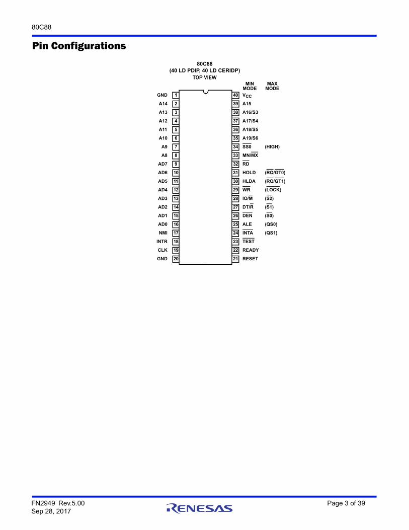
Pin Configurations
80C88(40 LD PDIP, 40 LD CERIDP)
TOP VIEW
13
1
2
3
4
5
6
7
8
9
10
11
12
14
15
16
17
18
19
20
GND
A14
A13
A12
A11
A10
A9
A8
AD7
AD6
AD5
AD4
AD3
AD2
AD1
AD0
NMI
INTR
CLK
GND
28
40
39
38
37
36
35
34
33
32
31
30
29
27
26
25
24
23
22
21
VCC
A15
A16/S3
A17/S4
A18/S5
A19/S6
SS0
MN/MX
RD
(RQ/GT0)
(RQ/GT1)
(LOCK)
(S2)
(S1)
(S0)
(QS0)
(QS1)
TEST
READY
RESET
INTA
ALE
DEN
DT/R
IO/M
WR
HLDA
HOLD
MIN MAX
(HIGH)
MODEMODE
FN2949 Rev.5.00 Page 3 of 39Sep 28, 2017

80C88
Functional Diagram
REGISTER FILEEXECUTION UNIT
CONTROL AND TIMING
INSTRUCTIONQUEUE
4-BYTE
FLAGS
16-BIT ALU
BUS 8
4
QS0, QS1
S2, S1, S0
2
4
3
GNDVCC
CLK RESET READY
BUS INTERFACE UNITRELOCATION
REGISTER FILE
3
A19/S6. . . A16/S3
INTA, RD, WR
DT/R, DEN, ALE, IO/M
SSO/HIGH
2
SEGMENT REGISTERSAND
INSTRUCTION POINTER(5 WORDS)
DATA POINTERAND
INDEX REGS(8 WORDS)
TESTINTRNMI
HLDAHOLD
RQ/GT0, 1
LOCK
MN/MX
3
ES
CS
SS
DSIP
AH
BH
CH
DH
AL
BL
CL
DL
SP
BP
SI
DI
ARITHMETIC/LOGIC UNIT
B-BUS
C-BUS
EXECUTIONUNIT
INTERFACEUNIT
BUS
QUEUE
INSTRUCTIONSTREAM BYTE
EXECUTION UNITCONTROL SYSTEM
FLAGS
MEMORY INTERFACE
A-BUS
AD7-AD0
8 A8-A15INTERFACE
UNIT
FN2949 Rev.5.00 Page 4 of 39Sep 28, 2017
80C88
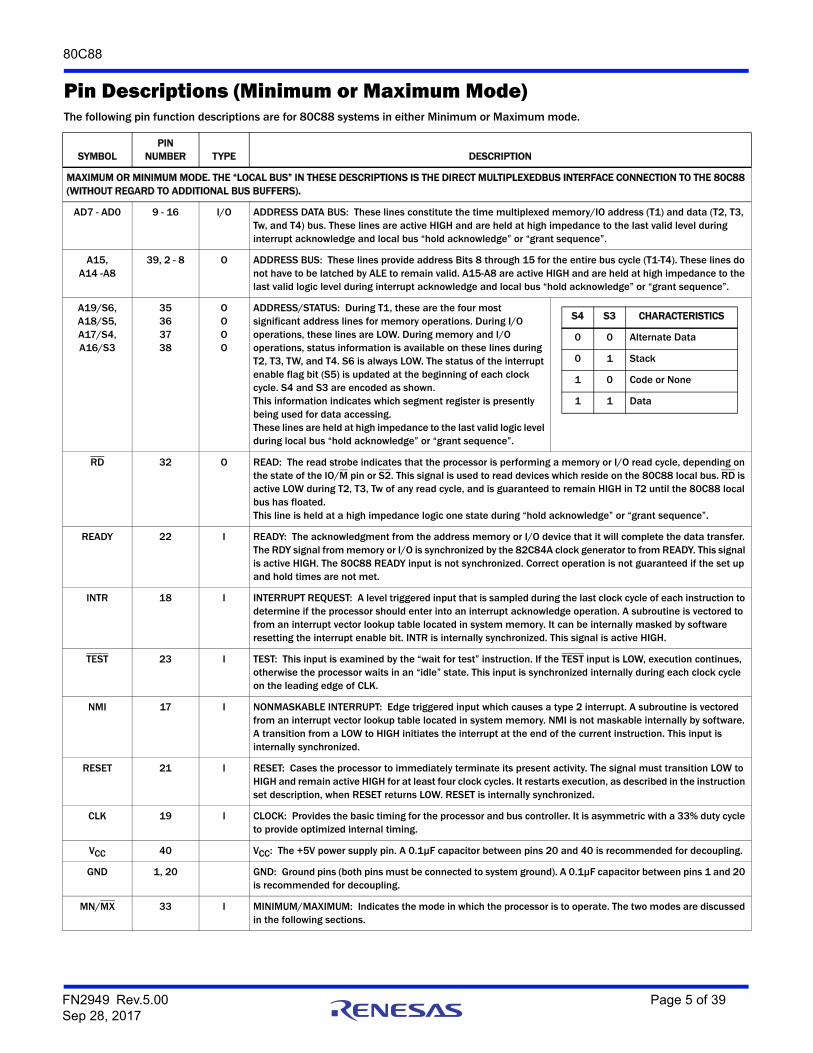
Pin Descriptions (Minimum or Maximum Mode)The following pin function descriptions are for 80C88 systems in either Minimum or Maximum mode.
SYMBOLPIN
NUMBER TYPE DESCRIPTION
MAXIMUM OR MINIMUM MODE. THE “LOCAL BUS” IN THESE DESCRIPTIONS IS THE DIRECT MULTIPLEXEDBUS INTERFACE CONNECTION TO THE 80C88 (WITHOUT REGARD TO ADDITIONAL BUS BUFFERS).
AD7 - AD0 9 - 16 I/O ADDRESS DATA BUS: These lines constitute the time multiplexed memory/IO address (T1) and data (T2, T3, Tw, and T4) bus. These lines are active HIGH and are held at high impedance to the last valid level during interrupt acknowledge and local bus “hold acknowledge” or “grant sequence”.
A15,A14 -A8
39, 2 - 8 O ADDRESS BUS: These lines provide address Bits 8 through 15 for the entire bus cycle (T1-T4). These lines do not have to be latched by ALE to remain valid. A15-A8 are active HIGH and are held at high impedance to the last valid logic level during interrupt acknowledge and local bus “hold acknowledge” or “grant sequence”.
A19/S6, A18/S5, A17/S4, A16/S3
35363738
OOOO
ADDRESS/STATUS: During T1, these are the four most significant address lines for memory operations. During I/O operations, these lines are LOW. During memory and I/O operations, status information is available on these lines during T2, T3, TW, and T4. S6 is always LOW. The status of the interrupt enable flag bit (S5) is updated at the beginning of each clock cycle. S4 and S3 are encoded as shown.This information indicates which segment register is presently being used for data accessing.These lines are held at high impedance to the last valid logic level during local bus “hold acknowledge” or “grant sequence”.
RD 32 O READ: The read strobe indicates that the processor is performing a memory or I/O read cycle, depending on the state of the IO/M pin or S2. This signal is used to read devices which reside on the 80C88 local bus. RD is active LOW during T2, T3, Tw of any read cycle, and is guaranteed to remain HIGH in T2 until the 80C88 local bus has floated.This line is held at a high impedance logic one state during “hold acknowledge” or “grant sequence”.
READY 22 I READY: The acknowledgment from the address memory or I/O device that it will complete the data transfer. The RDY signal from memory or I/O is synchronized by the 82C84A clock generator to from READY. This signal is active HIGH. The 80C88 READY input is not synchronized. Correct operation is not guaranteed if the set up and hold times are not met.
INTR 18 I INTERRUPT REQUEST: A level triggered input that is sampled during the last clock cycle of each instruction to determine if the processor should enter into an interrupt acknowledge operation. A subroutine is vectored to from an interrupt vector lookup table located in system memory. It can be internally masked by software resetting the interrupt enable bit. INTR is internally synchronized. This signal is active HIGH.
TEST 23 I TEST: This input is examined by the “wait for test” instruction. If the TEST input is LOW, execution continues, otherwise the processor waits in an “idle” state. This input is synchronized internally during each clock cycle on the leading edge of CLK.
NMI 17 I NONMASKABLE INTERRUPT: Edge triggered input which causes a type 2 interrupt. A subroutine is vectored from an interrupt vector lookup table located in system memory. NMI is not maskable internally by software. A transition from a LOW to HIGH initiates the interrupt at the end of the current instruction. This input is internally synchronized.
RESET 21 I RESET: Cases the processor to immediately terminate its present activity. The signal must transition LOW to HIGH and remain active HIGH for at least four clock cycles. It restarts execution, as described in the instruction set description, when RESET returns LOW. RESET is internally synchronized.
CLK 19 I CLOCK: Provides the basic timing for the processor and bus controller. It is asymmetric with a 33% duty cycle to provide optimized internal timing.
VCC 40 VCC: The +5V power supply pin. A 0.1µF capacitor between pins 20 and 40 is recommended for decoupling.
GND 1, 20 GND: Ground pins (both pins must be connected to system ground). A 0.1µF capacitor between pins 1 and 20 is recommended for decoupling.
MN/MX 33 I MINIMUM/MAXIMUM: Indicates the mode in which the processor is to operate. The two modes are discussed in the following sections.
S4 S3 CHARACTERISTICS
0 0 Alternate Data
0 1 Stack
1 0 Code or None
1 1 Data
FN2949 Rev.5.00 Page 5 of 39Sep 28, 2017
80C88
Pin Descriptions (Minimum Mode)The following pin function descriptions are for 80C88 systems in Minimum mode (MN/MX = VCC). Only the pin functions which are unique to the minimum mode are described; all other pin functions are as described above.
SYMBOLPIN
NUMBER TYPE DESCRIPTION
MINIMUM MODE SYSTEM (MN/MX = VCC)
IO/M 28 O STATUS LINE: An inverted Maximum mode S2. It distinguishes a memory access from an I/O access. IO/M becomes valid in the T4 preceding a bus cycle and remains valid until the final T4 of the cycle (I/O = HIGH, M = LOW). IO/M is held to a high impedance logic one during local bus “hold acknowledge”.
WR 29 O Write: Strobe indicating that the processor is performing a write memory or write I/O cycle, depending on the state of the IO/M signal. WR is active for T2, T3, and Tw of any write cycle. It is active LOW, and is held to high impedance logic one during local bus “hold acknowledge”.
INTA 24 O INTA: Used as a read strobe for interrupt acknowledge cycles. It is active LOW during T2, T3, and Tw of each interrupt acknowledge cycle. Note that INTA is never floated.
ALE 25 O ADDRESS LATCH ENABLE: Provided by the processor to latch the address into the 82C82/82C83 address latch. It is a HIGH pulse active during clock low of T1 of any bus cycle. Note that ALE is never floated.
DT/R 27 O DATA TRANSMIT/RECEIVE: Needed in a minimum system that uses an 82C86/82C87 data bus transceiver. It is controls the direction of data flow through the transceiver. Logically, DT/R is equivalent to S1 in the maximum mode, and its timing is the same as for IO/M (T = HIGH, R = LOW). This signal is held to a high impedance logic one during local bus “hold acknowledge”.
DEN 26 O DATA ENABLE: Provided as an output enable for the 82C86/82C87 in a minimum system which uses the transceiver. DEN is active LOW during each memory and I/O access, and for INTA cycles. For a read or INTA cycle, it is active from the middle of T2 until the middle of T4, while for a write cycle, it is active from the beginning of T2 until the middle of T4. DEN is held to high impedance logic one during local bus “hold acknowledge”.
HOLD,HLDA
3130
IO
HOLD: Indicates that another master is requesting a local bus “hold”. To be acknowledged, HOLD must be active HIGH. The processor receiving the “hold” request will issue HLDA (HIGH) as an acknowledgment, in the middle of a T4 or T1 clock cycle. Simultaneous with the issuance of HLDA, the processor will float the local bus and control lines. After HOLD is detected as being LOW, the processor lowers HLDA, and when the processor needs to run another cycle, it will again drive the local bus and control lines.Hold is not an asynchronous input. External synchronization should be provided if the system cannot otherwise guarantee the set up time.
SS0 34 O STATUS LINE: Is logically equivalent to S0 in Maximum mode. The combination of SS0, IO/M and DT/R allows the system to completely decode the current bus cycle status. SS0 is held to high impedance logic one during local bus “hold acknowledge”.
IO/M DT/R SS0 CHARACTERISTICS
1 0 0 Interrupt Acknowledge
1 0 1 Read I/O Port
1 1 0 Write I/O Port
1 1 1 Halt
0 0 0 Code Access
0 0 1 Read Memory
0 1 0 Write Memory
0 1 1 Passive
FN2949 Rev.5.00 Page 6 of 39Sep 28, 2017
80C88
Pin Description (Maximum Mode)The following pin function descriptions are for 80C88 systems in Maximum mode (MN/MX = GND). Only the pin functions which are unique to the maximum mode are described; all other pin functions are as described above.
SYMBOLPIN
NUMBER TYPE DESCRIPTION
MAXIMUM MODE SYSTEM (MN/MX = GND).
S0S1S2
262728
OOO
STATUS: Is active during clock high of T4, T1, and T2, and is returned to the passive state (1, 1, 1) during T3 or during Tw when READY is HIGH. This status is used by the 82C88 bus controller to generate all memory and I/O access control signals. Any change by S2, S1, or S0 during T4 is used to indicate the beginning of a bus cycle. The return to the passive state in T3 or Tw is used to indicate the end of a bus cycle. These signals are held at a high impedance logic one state during “grant sequence”.
RQ/GT0,RQ/GT1
3130
I/O REQUEST/GRANT: These pins are used by other local bus masters to force the processor to release the local bus at the end of the processor’s current bus cycle. Each pin is bidirectional with RQ/GT0 having higher priority than RQ/GT1. RQ/GT has internal bus-hold high circuitry and can be left unconnected if unused. The request/grant sequence is as follows (see RQ/GT Timing Sequence):A pulse of one CLK wide from another local bus master indicates a local bus request (“hold”) to the 80C88 (pulse 1).During a T4 or T1 clock cycle, a pulse one clock wide from the 80C88 to the requesting master (pulse 2), indicates that the 80C88 has allowed the local bus to float and that it will enter the “grant sequence” state at the next CLK. The CPUs bus interface unit is disconnected logically from the local bus during “grant sequence”.A pulse one CLK wide from the requesting master indicates to the 80C88 (pulse 3) that the “hold” request is about to end and that the 80C88 can reclaim the local bus at the next CLK. The CPU then enters T4 (or T1 if no bus cycles pending).Each master-master exchange of the local bus is a sequence of three pulses. There must be one idle CLK cycle after bus exchange. Pulses are active LOW.If the request is made while the CPU is performing a memory cycle, it will release the local bus during T4 of the cycle when all the following conditions are met:1. The request occurs on or before T2.2. The current cycle is not the low bit of a word.3. The current cycle is not the first acknowledge of an interrupt acknowledge sequence.A locked instruction is not currently executing.If the local bus is idle when the request is made the two possible events will follow:1. The local bus will be released during the next clock.2. A memory cycle will start within three clocks. Now the four rules for a currently active memory cycle apply with condition number 1 already satisfied.
LOCK 29 O LOCK: Indicates that other system bus masters must not gain control of the system bus while LOCK is active (LOW). The LOCK signal is activated by the “LOCK” prefix instruction and remains active until the completion of the next instruction. This signal is active LOW, and is held at a high impedance logic one state during “grant sequence”. In Maximum Mode, LOCK is automatically generated during T2 of the first INTA cycle and removed during T2 of the second INTA cycle.
QS1, QS0 24, 25 O QUEUE STATUS: Provides status to allow external tracking of the internal 80C88 instruction queue.The queue status is valid during the CLK cycle after which the queue operation is performed. Note that the queue status never goes to a high impedance statue (floated).
34 O Pin 34 is always a logic 1e in Maximum mode and is held at a high impedance logic 1 during a “grant sequence”.
S2 S1 S0 CHARACTERISTICS
0 0 0 Interrupt Acknowledge
0 0 1 Read I/O Port
0 1 0 Write I/O Port
0 1 1 Halt
1 0 0 Code Access
1 0 1 Read Memory
1 1 0 Write Memory
1 1 1 Passive
QS1 QS0 CHARACTERISTICS
0 0 No Operation
0 1 First Byte of Opcode from Queue
1 0 Empty the Queue
1 1 Subsequent Byte from Queue
FN2949 Rev.5.00 Page 7 of 39Sep 28, 2017

80C88
Functional DescriptionStatic OperationAll 80C88 circuitry is static in design. Internal registers, counters, and latches are static and do not require refresh as with dynamic circuit design. This eliminates the minimum operating frequency restriction placed on other microprocessors. The CMOS 80C88 can operate from DC to the specified upper frequency limit. The processor clock can be stopped in either state (high/low) and held there indefinitely. This type of operation is especially useful for system debug or power critical applications.
The 80C88 can be single stepped using only the CPU clock. This state can be maintained as long as is necessary. Single step clock operation allows simple interface circuitry to provide critical information for start-up.
Static design also allows very low frequency operation (as low as DC). In a power critical situation, this can provide extremely low power operation since 80C88 power dissipation is directly related to operation frequency. As the system frequency is reduced, so is the operating power until the power requirement is the 80C88 standby current at a DC input frequency.
Internal ArchitectureThe internal functions of the 80C88 processor are partitioned logically into two processing units. The first is the Bus Interface Unit (BIU) and the second is the Execution Unit (EU) as shown in the “Functional Diagram” on page 4.
These units can interact directly but for the most part perform as separate asynchronous operational processors. The BIU provides the functions related to instruction fetching and queuing, operand fetch and store, and address relocation. This unit also provides the basic bus control. The overlap of instruction pre-fetching provided by this unit serves to increase processor performance through improved bus bandwidth utilization. Up to four bytes of the instruction stream can be queued while waiting for decoding and execution.
The instruction stream queuing mechanism allows the BIU to keep the memory utilized very efficiently. Whenever there is space for at least one byte in the queue, the BIU will attempt a byte fetch memory cycle. This greatly reduces “dead time” on the memory bus. The queue acts as a First-In-First-Out (FIFO) buffer, from which the EU extracts instruction bytes as required. If the queue is empty (following a branch instruction, for example), the first byte into the queue immediately becomes available to the EU.
The execution unit receives pre-fetched instructions from the BIU queue and provides unrelocated operand addresses to the BIU. Memory operands are passed through the BIU for processing by the EU, which passes results to the BIU for storage.
Memory OrganizationThe processor provides a 20-bit address to memory which locates the byte being referenced. The memory is organized as a linear array of up to 1 million bytes, addressed as 00000(H) to FFFFF(H). The memory is logically divided into code, data, extra, and stack segments of up to 64 bytes each, with each segment falling on 16-byte boundaries (see Figure 1).
.
All memory references are made relative to base addresses contained in high speed segment registers. The segment types were chosen based on the addressing needs of programs. The segment register to be selected is automatically chosen according to specific rules as shown in Table 1. All information in one segment type shares the same logical attributes (for example, code or data). By structuring memory into relocatable areas of similar characteristics and by automatically selecting segment registers, programs are shorter, faster, and more structured.
Word (16-bit) operands can be located on even or odd address boundaries. For address and data operands, the least significant byte of the word is stored in the lower valued address location and the most significant byte in the next higher address location.
The BIU will automatically execute two fetch or write cycles for 16-bit operands.
Certain locations in memory are reserved for specific CPU operations, as shown in Figure 2 on page 9). Locations from
TABLE 1.
MEMORYREFERENCE
NEED
SEGMENTREGISTER
USEDSEGMENT
SELECTION RULE
Instructions CODE (CS) Automatic with all instruction prefetch.
Stack STACK (SS) All stack pushes and pops. Memory references relative to BP base register except data references.
Local Data DATA (DS) Data references when: relative to stack, destination of string operation, or explicitly overridden.
External Data(Global)
EXTRA (ES) Destination of string operations: Explicitly selected using a segment override.
SEGMENTREGISTER FILE
CS
SS
DS
ES
64K-BIT
+ OFFSET
FFFFFH
CODE SEGMENT
XXXXOH
STACK SEGMENT
DATA SEGMENT
EXTRA SEGMENT
00000H
FIGURE 1. MEMORY ORGANIZATION
MSB
BYTE
LSB
7 0
WORD
FN2949 Rev.5.00 Page 8 of 39Sep 28, 2017

80C88
addresses FFFF0H through FFFFFH are reserved for operations including a jump to initial system initialization routine. Following RESET, the CPU will always begin execution at location FFFF0H where the jump must be located. Locations 00000H through 003FFH are reserved for interrupt operations. Each of the 256 possible interrupt service routines is accessed through its own pair of 16-bit pointers - the segment address pointer and offset address pointer. The first pointer, used as the offset address, is loaded into the IP. The second pointer, which designates the base address, is loaded into the CS. At this point program control is transferred to the interrupt routine. The pointer elements are assumed to have been stored at their respective places in reserved memory before the occurrence of interrupts.
Minimum and Maximum ModesThe requirements for supporting minimum and maximum 80C88 systems are sufficiently different that they cannot be done efficiently with 40 uniquely defined pins. Consequently, the 80C88 is equipped with a strap pin (MN/MX) which defines the system configuration. The definition of a certain subset of the pins changes is dependent on the condition of the strap pin. When the MN/MX pin is strapped to GND, the 80C88 defines pins 24 through 31 and pin 34 in Maximum mode. When the
MN/MX pins are strapped to VCC, the 80C88 generates bus control signals itself on pins 24 through 31 and pin 34.
The minimum mode 80C88 can be used with either a multiplexed or demultiplexed bus. This architecture provides the 80C88 processing power in a highly integrated form.
The demultiplexed mode requires one latch (for 64k address ability) or two latches (for a full megabyte of addressing). An 82C86 or 82C87 transceiver can also be used if data bus buffering is required (see Figure 3 on page 10). The 80C88 provides DEN and DT/R to control the transceiver, and ALE to latch the addresses. This configuration of the minimum mode provides the standard demultiplexed bus structure with heavy bus buffering and relaxed bus timing requirements.
The maximum mode employs the 82C88 bus controller (see Figure 4 on page 11). The 82C88 decodes status lines S0, S1, and S2, and provides the system with all bus control signals. Moving the bus control to the 82C88 provides better source and sink current capability to the control lines, and frees the 80C88 pins for extended large system features. The 80C88 provides hardware lock, queue status, and two request/grant interfaces in Maximum mode. These features allow coprocessors in local bus and remote bus configurations.
TYPE 255 POINTER(AVAILABLE)
RESET BOOTSTRAPPROGRAM JUMP
TYPE 33 POINTER(AVAILABLE)
TYPE 32 POINTER(AVAILABLE)
TYPE 31 POINTER(AVAILABLE)
TYPE 5 POINTER(RESERVED)
TYPE 4 POINTEROVERFLOW
TYPE 3 POINTER1 BYTE INT INSTRUCTION
TYPE 2 POINTERNON MASKABLE
TYPE 1 POINTERSINGLE STEP
TYPE 0 POINTERDIVIDE ERROR
CS BASE ADDRESS
IP OFFSET
014H
010H
00CH
008H
004H
000H
07FH
080H
084H
FFFF0H
FFFFFH
3FFH
3FCH
AVAILABLEINTERRUPT
POINTERS(224)
DEDICATEDINTERRUPT
POINTERS(5)
RESERVEDINTERRUPT
POINTERS(27)
FIGURE 2. RESERVED MEMORY LOCATIONS
16-BITS
FN2949 Rev.5.00 Page 9 of 39Sep 28, 2017

80C88
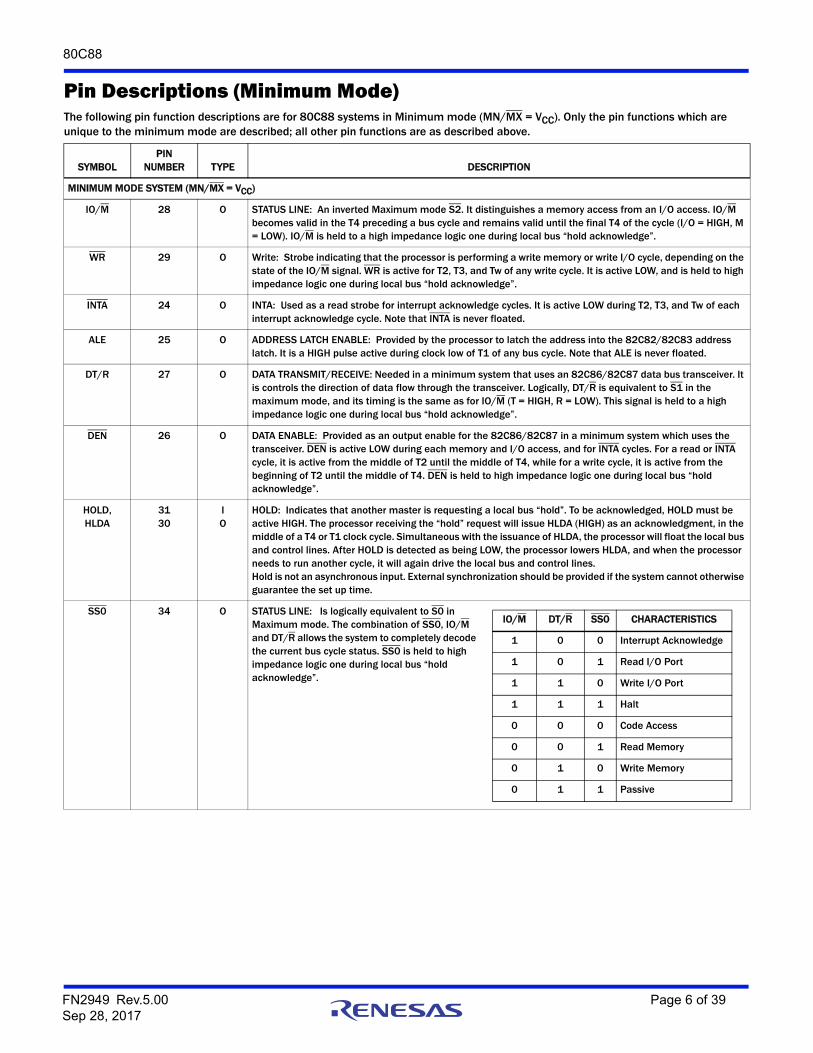
Bus OperationThe 80C88 address/data bus consists of three parts: the lower eight address/data bits (AD0-AD7), the middle eight address bits (A8-A15), and the upper four address bits (A16-A19). The address/data bits and the highest four address bits are time multiplexed. This technique provides the most efficient use of pins on the processor, permitting the use of standard 40 Ld package. The middle eight address bits are not multiplexed - they remain valid throughout each bus cycle. In addition, the bus can be demultiplexed at the processor with a single address latch if a standard, non multiplexed bus is desired for the system.
Each processor bus cycle consists of at least four CLK cycles. These are referred to as T1, T2, T3, and T4, as shown in Figure 5 on page 12. The address is emitted from the processor during T1 and data transfer occurs on the bus during T3 and T4. T2 is used primarily for changing the direction of the bus during read operations. In the event that a “Not Ready” indication is given by the addressed device, “wait” states (TW) are inserted between T3 and T4. Each inserted “wait” state is of the same duration as a
CLK cycle. Periods can occur between 80C88 driven bus cycles. These are referred to as “idle” states (TI), or inactive CLK cycles. The processor uses these cycles for internal housekeeping.
During T1 of any bus cycle, the ALE signal is emitted (by either the processor or the 82C88 bus controller, depending on the MN/MX strap). At the trailing edge of this pulse, a valid address and certain status information for the cycle can be latched.
Status bits S0, S1, and S2 are used by the bus controller while in Maximum mode to identify the type of bus transaction according to Table 2 on page 12.
Status bits S3 through S6 are multiplexed with high order address bits and are therefore valid during T2 through T4. S3 and S4 indicate which segment register was used to this bus cycle in forming the address according to Table 3 on page 12.
S5 is a reflection of the PSW interrupt enable bit. S6 is always equal to 0.
FIGURE 3. DEMULTIPLEXED BUS CONFIGURATION
RES
GND
82C84A/85
RDY
A8-A19AD0-AD7
80C88CPU
WR
RD
IO/MMN/MX
RESET
READY
CLK
VCCC1
C2
GND
GND1
20
40
C1 = C2 = 0.1F
VCC
VCC
DEN
DT/R
ALE
INTA
STB
OE
82C82LATCH
T
OE82C86
TRANSCEIVER
OE
HS-6616CMOS PROM
CS RDWR
82CXXPERIPHERALS
82C59AINTERRUPTCONTROL
GND
VCC
ADDR/DATA
INTR
ADDRESS
DATA
HM-65162CMOS PROM
IR0-7
(1, 2 OR 3)
INT
EN
CLOCKGENERATOR
FN2949 Rev.5.00 Page 10 of 39Sep 28, 2017

80C88
FIGURE 4. FULLY BUFFERED SYSTEM USING BUS CONTROLLER
RES
GND
82C84A/85
RDY
A8-A19AD0-AD7
80C88CPU
S2
S1
S0MN/MX
RESET
READY
CLK
VCCC1
C2
GND
GND1
20
40
C1 = C2 = 0.1F
GND
VCC
CLK
S0
S1S2DENDT/RALE
MRDC
MWTC
AMWC
IORC
IOWC
AIOWC
INTA
82C88
STB
OE
82C82LATCH
T
OE82C86
TRANSCEIVER
NC
NC
OE
HS-6616CMOS PROM
CS RDWR
82CXXPERIPHERALS
82C59AINTERRUPTCONTROL
GND
VCC
ADDR/DATA
INT
ADDRESS
DATA
HM-65162CMOS PROM
IR0-7
(1, 2 OR 3)
FN2949 Rev.5.00 Page 11 of 39Sep 28, 2017
80C88
I/O AddressingIn the 80C88, I/O operations can address up to a maximum of 64k I/O registers. The I/O address appears in the same format as the memory address on bus lines A15-A0. The address lines A19-A16 are zero in I/O operations. The variable I/O instructions, which use register DX as a pointer, have full address capability, while the direct I/O instructions directly address one or two of the 256 I/O byte locations in page 0 of the I/O address space. I/O ports are addressed in the same manner as memory locations.
FIGURE 5. BASIC SYSTEM TIMING
(4 + NWAIT) = TCY
T1 T2 T3 T4TWAIT T1 T2 T3 T4TWAIT
(4 + NWAIT) = TCY
GOES INACTIVE IN THE STATEJUST BEFORE T4
A19-A16 S6-S3
A7-A0 D15-D0VALID A7-A0 DATA OUT (D7-D0)
READYREADY
WAIT WAIT
MEMORY ACCESS TIME
ADDRSTATUS
CLK
ALE
S2-S0
ADDR DATA
RD, INTA
READY
DT/R
DEN
WP
S6-S3A19-A16
A15-A8ADDR A15-A8
BUS RESERVEDFOR DATA IN
TABLE 2.
S2 S1 S0 CHARACTERISTICS
0 0 0 Interrupt Acknowledge
0 0 1 Read I/O
0 1 0 Write I/O
0 1 1 Halt
1 0 0 Instruction Fetch
1 0 1 Read Data from Memory
1 1 0 Write Data to Memory
1 1 1 Passive (No Bus Cycle)
TABLE 3.
S4 S3 CHARACTERISTICS
0 0 Alternate Data (Extra Segment)
0 1 Stack
1 0 Code or None
1 1 Data
FN2949 Rev.5.00 Page 12 of 39Sep 28, 2017
80C88
Designers familiar with the 8085 or upgrading an 8085 design should note that the 8085 addresses I/O with an 8-bit address on both halves of the 16-bit address bus. The 80C88 uses a full 16-bit address on its lower 16 address lines.
External InterfaceProcessor Reset and InitializationProcessor initialization or start up is accomplished by activating (setting HIGH) the RESET pin. The 80C88 RESET is required to be HIGH for greater than four clock cycles. The 80C88 will terminate operations on the high-going edge of RESET and will remain dormant as long as RESET is HIGH. The low-going transition of RESET triggers an internal reset sequence for approximately seven clock cycles. After this interval the 80C88 operates normally, beginning with the instruction in absolute location FFFFOH (see Figure 2 on page 9). The RESET input is internally synchronized to the processor clock. At initialization, the HIGH to LOW transition of RESET must occur no sooner than 50µs after power up to allow complete initialization of the 80C88.
NMI will not be recognized if asserted before the second CLK cycle following the end of RESET.
Bus Hold CircuitryTo avoid high current conditions caused by floating inputs to CMOS devices and to eliminate the need for pull-up/down resistors, “bus-hold” circuitry has been used on 80C88 pins 2-16, 26-32, and 34-39 (see Figure 6A and 6B). These circuits maintain a valid logic state if no driving source is present (that is, an unconnected pin or a driving source which goes to a high impedance state).
To override the “bus hold” circuits, an external driver must be capable of supplying 400µA minimum sink or source current at valid input voltage levels. Since this “bus hold” circuitry is active and not a “resistive” type element, the associated power supply current is negligible. Power dissipation is significantly reduced when compared to the use of passive pull-up resistors.
Interrupt OperationsInterrupt operations fall into two classes: software initiated or hardware initiated. The software initiated interrupts and software aspects of hardware interrupts are specified in the instruction set description. Hardware interrupts can be classified as nonmusical or maskable.
Interrupts result in a transfer of control to a new program location. A 256 element table containing address pointers to the interrupt service program locations resides in absolute locations 0 through 3FFH (see Figure 2 on page 9), which are reserved for this purpose. Each element in the table is four bytes in size and corresponds to an interrupt “type”. An interrupting device supplies an 8-bit type number, during the interrupt acknowledge
sequence, which is used to vector through the appropriate element to the new interrupt service program location.
Non-Maskable Interrupt (NMI)The processor provides a single non-maskable interrupt (NMI) pin which has higher priority than the maskable interrupt request (INTR) pin. A typical use would be to activate a power failure routine. The NMI is edge-triggered on a LOW to HIGH transition. The activation of this pin causes a type 2 interrupt.
NMI is required to have a duration of greater than two cycles in the HIGH state but is not required to be synchronized to the clock. A high-going transition of NMI is latched on-chip and will be serviced at the end of the current instruction or between whole moves (2-bytes in the case of word moves) of a block type instruction. Worst case response to NMI would be for multiply, divide, and variable shift instructions. There is no specification on the occurrence of the low-going edge; it can occur before, during, or after the servicing of NMI. Another high-going edge triggers another response if it occurs after the start of the NMI procedure.
The signal must be free of logical spikes in general and be free of bounces on the low-going edge to avoid triggering extraneous responses.
Maskable Interrupt (INTR)The 80C88 provides a singe interrupt request input (INTR) which can be masked internally by software with the resetting of the interrupt enable (IF) flag bit. The interrupt request signal is level triggered. It is internally synchronized during each clock cycle on the high-going edge of CLK.
To receive a response, INTR must be present (HIGH) during the clock period preceding the end of the current instruction or the end of a whole move for a block type instruction. INTR can be removed anytime after the falling edge of the first INTA signal. During the interrupt response sequence, further interrupts are
FIGURE 6A. BUS HOLD CIRCUITRY PINS 2-16 AND 35-39
FIGURE 6B. BUS HOLD CIRCUITRY PINS 26-32 AND 34
FIGURE 6.
OUTPUTDRIVER
INPUTBUFFER
INPUTPROTECTIONCIRCUITRY
BONDPAD
EXTERNALPIN
OUTPUTDRIVER
INPUTBUFFER
INPUTPROTECTIONCIRCUITRY
BONDPAD
EXTERNALPIN
PVCC
FN2949 Rev.5.00 Page 13 of 39Sep 28, 2017
80C88
disabled. The enable bit is reset as part of the response to any interrupt (INTR, NMI, software interrupt, or single step). The FLAGS register, which is automatically pushed onto the stack, reflects the state of the processor before the interrupt. The enable bit will be zero until the old FLAGS register is restored, unless specifically set by an instruction.
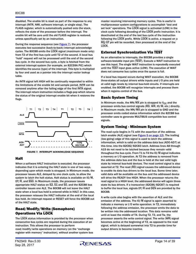
During the response sequence (see Figure 7), the processor executes two successive (back-to-back) interrupt acknowledge cycles. The 80C88 emits the LOCK signal (maximum mode only) from T2 of the first bus cycle until T2 of the second. A local bus “hold” request will not be processed until the end of the second bus cycle. In the second bus cycle, a byte is fetched from the external interrupt system (for example, an 82C59A PIC) which identifies the source (type) of the interrupt. This byte is multiplied by four and used as a pointer into the interrupt vector lookup table.
An INTR signal left HIGH will be continually responded to within the limitations of the enable bit and sample period. INTR can be removed anytime after the falling edge of the first INTA signal. The interrupt return instruction includes a flags pop which returns the status of the original interrupt enable bit when it restores the flags.
HaltWhen a software HALT instruction is executed, the processor indicates that it is entering the HALT state in one of two ways, depending upon which mode is strapped. In Minimum mode, the processor issues ALE, delayed by one clock cycle, to allow the system to latch the halt status. Halt status is available on IO/M, DT/R, and SS0. In Maximum mode, the processor issues appropriate HALT status on S2, S1 and S0, and the 82C88 bus controller issues one ALE. The 80C88 will not leave the HALT state when a local bus hold is entered while in HALT. In this case, the processor reissues the HALT indicator at the end of the local bus hold. An interrupt request or RESET will force the 80C88 out of the HALT state.
Read/Modify/Write (Semaphore) Operations Via LOCKThe LOCK status information is provided by the processor when consecutive bus cycles are required during the execution of an instruction. This allows the processor to perform read/modify/write operations on memory (on the “exchange register with memory” instruction), without another system bus
master receiving intervening memory cycles. This is useful in multiprocessor system configurations to accomplish “test and set lock” operations. The LOCK signal is activated (LOW) in the clock cycle following decoding of the LOCK prefix instruction. It is deactivated at the end of the last bus cycle of the instruction following the LOCK prefix. While LOCK is active, a request on a RQ/GT pin will be recorded, then processed at the end of the LOCK.
External Synchronization Via TESTAs an alternative to interrupts, the 80C88 provides a single software-testable input pin (TEST). Execute a WAIT instruction to use this input. The single WAIT instruction is repeatedly executed until the TEST input goes active (LOW). The execution of WAIT does not consume bus cycles once the queue is full.
If a local bus request occurs during WAIT execution, the 80C88 three-states all output drivers while inputs and I/O pins are held at valid logic levels by internal bus-hold circuits. If interrupts are enabled, the 80C88 will recognize interrupts and process them when it regains control of the bus.
Basic System TimingIn Minimum mode, the MN/MX pin is strapped to VCC and the processor emits bus control signals (RD, WR, IO/M, etc.) directly. In Maximum mode, the MN/MX pin is strapped to GND and the processor emits coded status information which the 82C88 bus controller uses to generate MULTIBUS compatible bus control signals.
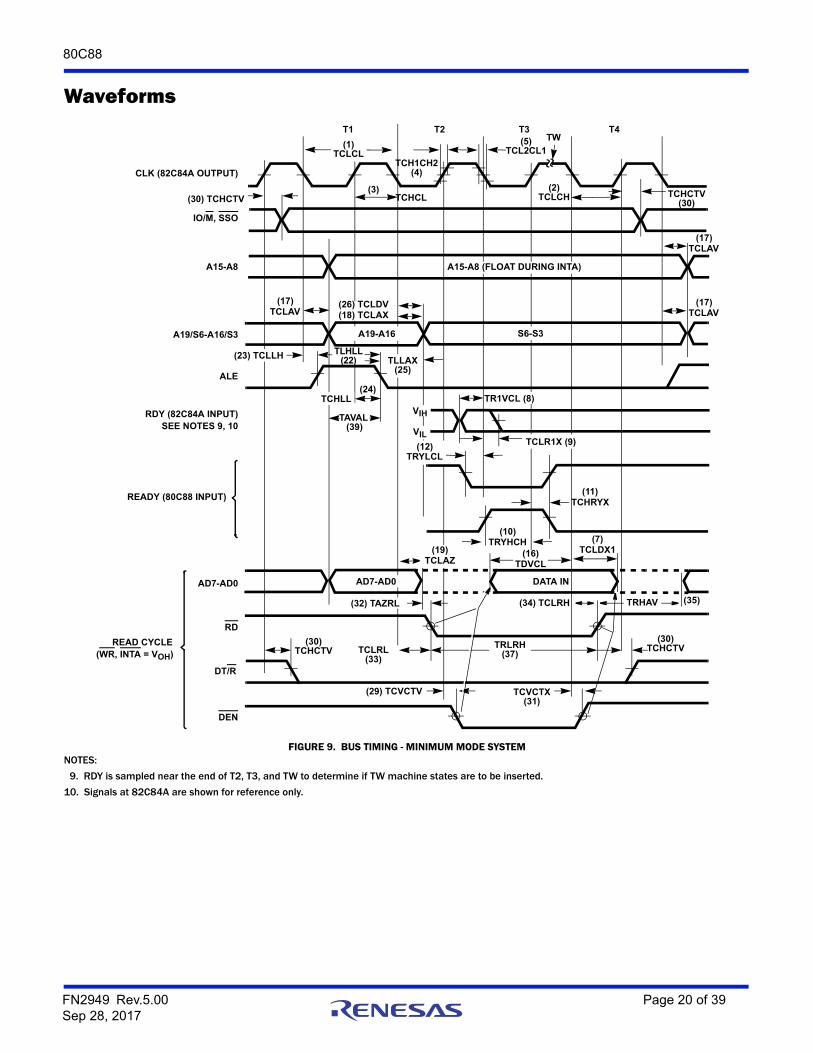
System Timing - Minimum SystemThe read cycle begins in T1 with the assertion of the address latch enable (ALE) signal (see Figure 5 on page 12). The trailing (low-going) edge of this signal is used to latch the address information, which is valid on the address data bus (ADO-AD7) at this time, into the 82C82/82C83 latch. Address lines A8 through A15 do not need to be latched because they remain valid throughout the bus cycle. From T1 to T4 the IO/M signal indicates a memory or I/O operation. At T2 the address is removed from the address data bus and the bus is held at the last valid logic state by internal bus-hold devices. The read control signal is also asserted at T2. The read (RD) signal causes the addressed device to enable its data bus drivers to the local bus. Some time later, valid data will be available on the bus and the addressed device will drive the READY line HIGH. When the processor returns the read signal to a HIGH level, the addressed device will again three-state its bus drivers. If a transceiver (82C86/82C87) is required to buffer the local bus, signals DT/R and DEN are provided by the 80C88.
A write cycle also begins with the assertion of ALE and the emission of the address. The IO/M signal is again asserted to indicate a memory or I/O write operation. In T2, immediately following the address emission, the processor emits the data to be written into the addressed location. This data remains valid until at least the middle of T4. During T2, T3, and Tw, the processor asserts the write control signal. The write (WR) signal becomes active at the beginning of T2, as opposed to the read signal, which is delayed somewhat into T2 to provide time for output drivers to become inactive.
FIGURE 7. INTERRUPT ACKNOWLEDGE SEQUENCE
ALE
LOCK
INTA
AD0- TYPE AD7
T1 T2 T3 T4 T1 T2 T3 T4
VECTOR
FN2949 Rev.5.00 Page 14 of 39Sep 28, 2017
80C88
The basic difference between the interrupt acknowledge cycle and a read cycle is that the interrupt acknowledge (INTA) signal is asserted in place of the read (RD) signal and the address bus is held at the last valid logic state by internal bus-hold devices (see Figure 6 on page 13. In the second of two successive INTA cycles, a byte of information is read from the data bus, as supplied by the interrupt system logic (i.e., 82C59A priority interrupt controller). This byte identifies the source (type) of the interrupt. It is multiplied by four and used as a pointer into the interrupt vector lookup table, as described earlier.
Bus Timing - Medium Complexity SystemsFor medium complexity systems, the MN/MX pin is connected to GND and the 82C88 bus controller is added to the system, as well as an 82C82/82C83 latch for latching the system address, and an 82C86/82C87 transceiver to allow for bus loading greater than the 80C88 is capable of handling (see Figure 8 on page 16). Signals ALE, DEN, and DT/R are generated by the 82C88 instead of the processor in this configuration, although their timing remains relatively the same. The 80C88 status outputs (S2, S1, and S0) provide the type of cycle information and become 82C88 inputs. This bus cycle information specifies a read (code, data, or I/O), write (data or I/O), interrupt acknowledge, or software halt. The 82C88 thus issues control signals specifying memory read or write, I/O read or write, or interrupt acknowledge. The 82C88 provides two types of write strobes, normal and advanced, to be applied as required. The normal write strobes have data valid at the leading edge of write. The advanced write strobes have the same timing as read strobes, and hence, data is not valid at the leading edge of write. The 82C86/82C87 transceiver receives the usual T and OE inputs from the 82C88 DT/R and DEN outputs.
The pointer into the interrupt vector table, which is passed during the second INTA cycle, can derive from an 82C59A located on either the local bus or the system bus. If the master 82C59A priority interrupt controller is positioned on the local bus, the 82C86/82C87 transceiver must be disabled when reading from the master 82C59A during the interrupt acknowledge sequence and software “poll”.
The 80C88 Compared to the 80C86The 80C88 CPU is an 8-bit processor designed around the 8086 internal structure. Most internal functions of the 80C88 are identical to the equivalent 80C86 functions. The 80C88 handles the external bus the same way the 80C86 does with the distinction of handling only 8-bits at a time. Sixteen-bit operands are fetched or written in two consecutive bus cycles. Both processors will appear identical to the software engineer, with
the exception of execution time. The internal register structure is identical and all instructions have the same end result. Internally, there are three differences between the 80C88 and the 80C86. All changes are related to the 8-bit bus interface.
• The queue length is four bytes in the 80C88, whereas the 80C86 queue contains six bytes, or three words. The queue was shortened to prevent overuse of the bus by the BIU when prefetching instructions. This was required because of the additional time necessary to fetch instructions eight bits at a time.
• To further optimize the queue, the prefetching algorithm was changed. The 80C88 BIU will fetch a new instruction to load into the queue each time there is a 1-byte space available in the queue. The 80C86 waits until a 2-byte space is available.
The internal execution time of the instruction set is affected by the 8-bit interface. All 16-bit fetches and writes from/to memory take an additional four clock cycles. The CPU is also limited by the speed of instruction fetches. This latter problem occurs only when a series of simple operations occur. When the more sophisticated instructions of the 80C88 are being used, the queue has time to fill the execution proceeds as fast as the execution unit will allow.
The 80C88 and 80C86 are completely software compatible by virtue of their identical execution units. Software that is system dependent may not be completely transferable, but software that is not system dependent will operate equally as well on an 80C88 or an 80C86.
The hardware interface of the 80C88 contains the major differences between the two CPUs. The pin assignments are nearly identical, however, with the following functional changes:
• A8-A15: These pins are only address outputs on the 80C88. These address lines are latched internally and remain valid throughout a bus cycle in a manner similar to the 8085 upper address lines.
• BHE has no meaning on the 80C88 and has been eliminated.
• SS0 provides the S0 status information in Minimum mode. This output occurs on pin 34 in Minimum mode only. DT/R, IO/M and SS0 provide the complete bus status in Minimum mode.
• IO/M has been inverted to be compatible with the 8085 bus structure.
• ALE is delayed by one clock cycle in Minimum mode when entering HALT, to allow the status to be latched with ALE.
FN2949 Rev.5.00 Page 15 of 39Sep 28, 2017

80C88
T1 T2 T3 T4
A7-A0 DATA IN
CLK
QS1, QS0
S2, S1, S0
A19/S6 - A16/S3
ALE
80C88
AD7 - AD0
DEN
S6 - S3
DT/R
MRDC
82C84RDY
READY
80C88
A19 - A16
A15 - A8
FIGURE 8. MEDIUM COMPLEXITY SYSTEM TIMING
RD
A15 - A880C88
80C88
80C88
DATA OUT
FN2949 Rev.5.00 Page 16 of 39Sep 28, 2017
80C88
Absolute Maximum Ratings Thermal InformationSupply Voltage . . . . . . . . . . . . . . . . . . . . . . . . . . . . . . . . . . . . . . . . . . . . +8.0VInput, Output or I/O Voltage . . . . . . . . . . . . . . . . . GND - 0.5V to VCC + 0.5VESD Classification. . . . . . . . . . . . . . . . . . . . . . . . . . . . . . . . . . . . . . . . . Class 1
Operating ConditionsOperating Voltage Range. . . . . . . . . . . . . . . . . . . . . . . . . . . . .+4.5V to +5.5V
M80C88-2 Only. . . . . . . . . . . . . . . . . . . . . . . . . . . . . . . . +4.75V to +5.25VOperating Temperature Range
C80C88/-2 . . . . . . . . . . . . . . . . . . . . . . . . . . . . . . . . . . . . . . 0°C to +70°CM80C88. . . . . . . . . . . . . . . . . . . . . . . . . . . . . . . . . . . . . . .-55°C to +125°C
Thermal Resistance (Typical) . . . . . . . . . . . . . . . . . . . . . . . . . . . . JA (oC/W)PDIP Package* . . . . . . . . . . . . . . . . . . . . . . . . . . . . . . . . . . . . . . . . . . . . .50CERDIP Package . . . . . . . . . . . . . . . . . . . . . . . . . . . . . . . . . . . . . . . . . . . .30
Maximum Junction TemperatureCeramic Package. . . . . . . . . . . . . . . . . . . . . . . . . . . . . . . . . . . . . . . +175°CPlastic Package . . . . . . . . . . . . . . . . . . . . . . . . . . . . . . . . . . . . . . . . +150°C
Storage Temperature Range . . . . . . . . . . . . . . . . . . . . . . . -65°C to +150°CPb-free reflow profile . . . . . . . . . . . . . . . . . . . . . . . . . . . . . . . . refer to TB493*Pb-free PDIPs can be used for through hole wave solder processing only.They are not intended for use in Reflow solder processing applications.
Die CharacteristicsGate Count . . . . . . . . . . . . . . . . . . . . . . . . . . . . . . . . . . . . . . . . . . .9750 Gates
CAUTION: Do not operate at or near the maximum ratings listed for extended periods of time. Exposure to such conditions can adversely impact productreliability and result in failures not covered by warranty.
Electrical SpecificationsVCC = 5.0V, ±10%; TA = 0°C to +70°C (C80C88, C80C88-2)VCC = 5.0V, ±10%; TA = -55°C to +125°C (M80C88)
SYMBOL PARAMETER TEST CONDITION MIN MAX UNITS
VlH Logical One Input Voltage C80C88 (Note 4) 2.0 - V
M80C88 (Note 4) 2.2 V
VIL Logical Zero Input Voltage - 0.8 V
VIHC CLK Logical One Input Voltage VCC - 0.8 - V
VILC CLK Logical Zero Input Voltage - 0.8 V
VOH Output High Voltage lOH = -2.5mA 3.0 - V
lOH = -100µA VCC - 0.4 V
VOL Output Low Voltage lOL = +2.5mA - 0.4 V
II Input Leakage Current VIN = 0V or VCCPins 17 through 19, 21 through 23, and 33
-1.0 1.0 µA
lBHH Input Current-Bus Hold High VIN = - 3.0V (Note 1) -40 -400 µA
lBHL Input Current-Bus Hold Low VIN = - 0.8V (Note 2) 40 400 µA
IO Output Leakage Current VOUT = 0V (Note 5) - -10.0 µA
ICCSB Standby Power Supply Current VCC = 5.5V (Note 3) - 500 µA
ICCOP Operating Power Supply Current FREQ = Max, VIN = VCC or GND,Outputs Open
- 10 mA/MHz
NOTES:
1. lBHH should be measured after raising VIN to VCC and then lowering to 3.0V on the following pins 2 through 16, 26 through 32, 34 through 39.
2. IBHL should be measured after lowering VIN to GND and then raising to 0.8V on the following pins: 2 through16, 35 through 39.
3. lCCSB tested during clock high time after HALT instruction executed. VIN = VCC or GND, VCC = 5.5V, outputs unloaded.
4. MN/MX is a strap option and should be held to VCC or GND.
5. IO should be measured by putting the pin in a high impedance state and then driving VOUT to GND on the following pins: 26-29 and 32.
Capacitance TA = +25°C
SYMBOL PARAMETER TEST CONDITIONS TYPICAL UNITS
CIN Input Capacitance FREQ = 1MHz. All measurements are referenced to device GND 25 pF
COUT Output Capacitance FREQ = 1MHz. All measurements are referenced to device GND 25 pF
CI/O I/O Capacitance FREQ = 1MHz. All measurements are referenced to device GND 25 pF
FN2949 Rev.5.00 Page 17 of 39Sep 28, 2017

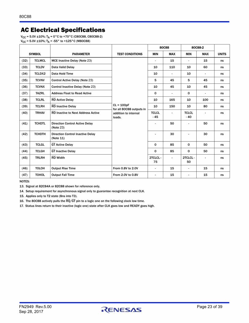
80C88
AC Electrical SpecificationsVCC = 5.0V ±10%; TA = 0°C to +70°C (C80C88, C80C88-2)VCC = 5.0V ±10%; TA = -55° to +125°C (M80C88)
SYMBOL PARAMETERTEST
CONDITIONS
80C88 80C88-2
UNITSMIN MAX MIN MAX
MINIMUM COMPLEXITY SYSTEM
Timing Requirements
(1) TCLCL CLK Cycle Period 200 - 125 - ns
(2) TCLCH CLK Low Time 118 - 68 - ns
(3) TCHCL CLK High Time 69 - 44 - ns
(4) TCH1CH2 CLK Rise Time From 1.0V to 3.5V - 10 - 10 ns
(5) TCL2CL1 CLK FaIl Time From 3.5V to 1.0V - 10 - 10 ns
(6) TDVCL Data In Setup Time 30 - 20 - ns
(7) TCLDX1 Data In Hold Time 10 - 10 - ns
(8) TR1VCL RDY Setup Time into 82C84A (Notes 6,7)
35 - 35 - ns
(9) TCLR1X RDY Hold Time into 82C84A (Notes 6,7)
0 - 0 - ns
(10) TRYHCH READY Setup Time into 80C88 118 - 68 - ns
(11) TCHRYX READY Hold Time into 80C88 30 - 20 - ns
(12) TRYLCL READY Inactive to CLK (Note 8) -8 - -8 - ns
(13) THVCH HOLD Setup Time 35 - 20 - ns
(14) TINVCH lNTR, NMI, TEST Setup Time(Note 7)
30 - 15 - ns
(15) TILIH Input Rise Time (Except CLK) From 0.8V to 2.0V - 15 - 15 ns
(16) TIHIL Input FaIl Time (Except CLK) From 2.0V to 0.8V - 15 - 15 ns
Timing Responses
(17) TCLAV Address Valid Delay CL = 100pF 10 110 10 60 ns
(18) TCLAX Address Hold Time CL = 100pF 10 - 10 - ns
(19) TCLAZ Address Float Delay CL = 100pF TCLAX 80 TCLAX 50 ns
(20) TCHSZ Status Float Delay CL = 100pF - 80 - 50 ns
(21) TCHSV Status Active Delay CL = 100pF 10 110 10 60 ns
(22) TLHLL ALE Width CL = 100pF TCLCH-20 - TCLCH-10 - ns
(23) TCLLH ALE Active Delay CL = 100pF - 80 - 50 ns
(24) TCHLL ALE Inactive Delay CL = 100pF - 85 - 55 ns
(25) TLLAX Address Hold Time to ALE Inactive CL = 100pF TCHCL-10 - TCHCL-10 - ns
(26) TCLDV Data Valid Delay CL = 100pF 10 110 10 60 ns
(27) TCLDX2 Data Hold Time CL = 100pF 10 - 10 - ns
(28) TWHDX Data Hold Time After WR CL = 100pF TCLCL-30 - TCLCL-30 - ns
(29) TCVCTV Control Active Delay 1 CL = 100pF 10 110 10 70 ns
(30) TCHCTV Control Active Delay 2 CL = 100pF 10 110 10 60 ns
(31) TCVCTX Control Inactive Delay CL = 100pF 10 110 10 70 ns
(32) TAZRL Address Float to READ Active CL = 100pF 0 - 0 - ns
FN2949 Rev.5.00 Page 18 of 39Sep 28, 2017

80C88
(33) TCLRL RD Active Delay CL = 100pF 10 165 10 100 ns
(34) TCLRH RD Inactive Delay CL = 100pF 10 150 10 80 ns
(35) TRHAV RD Inactive to Next Address Active CL = 100pF TCLCL-45 - TCLCL-40 - ns
(36) TCLHAV HLDA Valid Delay CL = 100pF 10 160 10 100 ns
(37) TRLRH RD Width CL = 100pF 2TCLCL-75 - 2TCLCL-50 - ns
(38) TWLWH WR Width CL = 100pF 2TCLCL-60 - 2TCLCL-40 - ns
(39) TAVAL Address Valid to ALE Low CL = 100pF TCLCH-60 - TCLCH-40 - ns
(40) TOLOH Output Rise Time From 0.8V to 2.0V - 15 - 15 ns
(41) TOHOL Output Fall Time From 2.0V to 0.8V - 15 - 15 ns
NOTES:
6. Signal at 82C84A shown for reference only.
7. Setup requirement for asynchronous signal only to guarantee recognition at next CLK.
8. Applies only to T2 state (8ns into T3).
AC Electrical SpecificationsVCC = 5.0V ±10%; TA = 0°C to +70°C (C80C88, C80C88-2)VCC = 5.0V ±10%; TA = -55° to +125°C (M80C88)
SYMBOL PARAMETERTEST
CONDITIONS
80C88 80C88-2
UNITSMIN MAX MIN MAX
FN2949 Rev.5.00 Page 19 of 39Sep 28, 2017
80C88
Waveforms
FIGURE 9. BUS TIMING - MINIMUM MODE SYSTEMNOTES:
9. RDY is sampled near the end of T2, T3, and TW to determine if TW machine states are to be inserted.
10. Signals at 82C84A are shown for reference only.
TCVCTX(31)
(29) TCVCTV
DEN
DT/R
(30)TCHCTV TCLRL
(33)
(30)TCHCTV
READ CYCLE
(35)(34) TCLRH
RD
DATA IN
(7)TCLDX1
(10)TRYHCH
AD7-AD0
(24)
(17)TCLAV
READY (80C88 INPUT)
RDY (82C84A INPUT)SEE NOTES 9, 10
ALE
A19/S6-A16/S3
(17)TCLAV
IO/M, SSO
(30) TCHCTV
CLK (82C84A OUTPUT)
(3)TCHCL
TCH1CH2(4)
(2)TCLCH TCHCTV
(30)
(5)TCL2CL1
T1 T2 T3TW
T4
(WR, INTA = VOH)
(1)TCLCL
(26) TCLDV(18) TCLAX
A19-A16
(23) TCLLH TLHLL(22) TLLAX
(25)
TCHLL
TAVAL(39) VIL
VIH
(12)TRYLCL
(11)TCHRYX
(19)TCLAZ
(16)TDVCL
AD7-AD0
TRHAV(32) TAZRL
TRLRH(37)
TCLR1X (9)
TR1VCL (8)
S6-S3
(17)TCLAV
A15-A8 A15-A8 (FLOAT DURING INTA)
FN2949 Rev.5.00 Page 20 of 39Sep 28, 2017
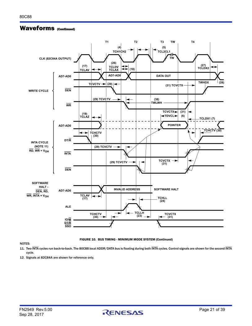
80C88
FIGURE 10. BUS TIMING - MINIMUM MODE SYSTEM (Continued)NOTES:
11. Two INTA cycles run back-to-back. The 80C88 local ADDR/DATA bus is floating during both INTA cycles. Control signals are shown for the second INTA cycle.
12. Signals at 82C84A are shown for reference only.
Waveforms (Continued)
T4T3T2T1
TW
TCLDX1 (7)
TWHDX
TCVCTX
TCHCTV (30)
TCLAV
TCLAZ
TCHCTV
(31) TCVCTXTCVCTV
(17)(26)
(27)
(29) TCVCTV
DATA OUTAD7-AD0
INVALID ADDRESS
CLK (82C84A OUTPUT)
WRITE CYCLE
AD7-AD0
DEN
WR
INTA CYCLE
(NOTE 11)
RD, WR = VOH
AD7-AD0
DT/R
INTA
DEN
AD7-AD0
SOFTWAREHALT -
DEN, RD,
WR, INTA = VOH
SOFTWARE HALT
(29) TCVCTV
POINTER
TCL2CL1
(5)
TW
TCLAVTCLDVTCLAX (18) TCLDX2
(29) (28)
(29) TCVCTV
(19)TCVCTX
(6)
(30)
(31)
(17)
TCH1CH2
(4)
ALE
IO/MDT/RSSO
TCLLH(23)
TCHLL(24)
TCVCTX(31)
TCHCTV(30)
TDVCL
(31)
TWLWH(38)
FN2949 Rev.5.00 Page 21 of 39Sep 28, 2017

80C88
AC Electrical SpecificationsVCC = 5.0V ±10%; TA = 0°C to +70°C (C80C88, C80C88-2)VCC = 5.0V ±10%; TA = -55° to +125°C (M80C88)
SYMBOL PARAMETER TEST CONDITIONS
80C88 80C88-2
UNITSMIN MAX MIN MAX
TIMING REQUIREMENTS
(1) TCLCL CLK Cycle Period 200 - 125 - ns
(2) TCLCH CLK Low Time 118 - 68 - ns
(3) TCHCL CLK High Time 69 - 44 - ns
(4) TCH1CH2 CLK Rise Time From 1.0V to 3.5V - 10 - 10 ns
(5) TCL2CL1 CLK Fall Time From 3.5V to 1.0V - 10 - 10 ns
(6) TDVCL Data in Setup Time 30 - 20 - ns
(7) TCLDX1 Data In Hold Time 10 - 10 - ns
(8) TR1VCL RDY Setup Time into 82C84(Notes 23,24)
35 - 35 - ns
(9) TCLR1X RDY Hold Time into 82C84(Notes 23,24)
0 - 0 - ns
(10) TRYHCH READY Setup Time into 80C88 118 - 68 - ns
(11) TCHRYX READY Hold Time into 80C88 30 - 20 - ns
(12) TRYLCL READY Inactive to CLK (Note25) -8 - -8 - ns
(13) TlNVCH Setup Time for Recognition (lNTR, NMl, TEST) (Note 24)
30 - 15 - ns
(14) TGVCH RQ/GT Setup Time 30 - 15 - ns
(15) TCHGX RQ Hold Time into 80C88 (Note 26) 40 TCHCL + 10
30 TCHCL + 10
ns
(16) TILlH Input Rise Time (Except CLK) From 0.8V to 2.0V - 15 - 15 ns
(17) TIHIL Input Fall Time (Except CLK) From 2.0V to 0.8V - 15 - 15 ns
TIMING RESPONSES
(18) TCLML Command Active Delay (Note23)
CL = 100pFfor all 80C88 outputs in addition to internal loads.
5 35 5 35 ns
(19) TCLMH Command Inactive (Note 23) 5 35 5 35 ns
(20) TRYHSH READY Active to Status Passive (Notes 25, 27)
- 110 - 65 ns
(21) TCHSV Status Active Delay 10 110 10 60 ns
(22) TCLSH Status Inactive Delay (Note 27) 10 130 10 70 ns
(23) TCLAV Address Valid Delay 10 110 10 60 ns
(24) TCLAX Address Hold Time 10 - 10 - ns
(25) TCLAZ Address Float Delay TCLAX 80 TCLAX 50 ns
(26) TCHSZ Status Float Delay - 80 - 50 ns
(27) TSVLH Status Valid to ALE High (Note 23) - 20 - 20 ns
(28) TSVMCH Status Valid to MCE High (Note 23) - 30 - 30 ns
(29) TCLLH CLK Low to ALE Valid (Note 23) - 20 - 20 ns
(30) TCLMCH CLK Low to MCE High (Note 23) - 25 - 25 ns
(31) TCHLL ALE Inactive Delay (Note 23) 4 18 4 18 ns
FN2949 Rev.5.00 Page 22 of 39Sep 28, 2017
80C88
(32) TCLMCL MCE Inactive Delay (Note 23)
CL = 100pFfor all 80C88 outputs in addition to internal loads.
- 15 - 15 ns
(33) TCLDV Data Valid Delay 10 110 10 60 ns
(34) TCLDX2 Data Hold Time 10 - 10 - ns
(35) TCVNV Control Active Delay (Note 23) 5 45 5 45 ns
(36) TCVNX Control Inactive Delay (Note 23) 10 45 10 45 ns
(37) TAZRL Address Float to Read Active 0 - 0 - ns
(38) TCLRL RD Active Delay 10 165 10 100 ns
(39) TCLRH RD Inactive Delay 10 150 10 80 ns
(40) TRHAV RD Inactive to Next Address Active TCLCL- 45
- TCLCL- 40
- ns
(41) TCHDTL Direction Control Active Delay(Note 23)
- 50 - 50 ns
(42) TCHDTH Direction Control Inactive Delay(Note 11)
- 30 - 30 ns
(43) TCLGL GT Active Delay 0 85 0 50 ns
(44) TCLGH GT Inactive Delay 0 85 0 50 ns
(45) TRLRH RD Width 2TCLCL - 75
- 2TCLCL - 50
- ns
(46) TOLOH Output Rise Time From 0.8V to 2.0V - 15 - 15 ns
(47) TOHOL Output Fall Time From 2.0V to 0.8V - 15 - 15 ns
NOTES:
13. Signal at 82C84A or 82C88 shown for reference only.
14. Setup requirement for asynchronous signal only to guarantee recognition at next CLK.
15. Applies only to T2 state (8ns into T3).
16. The 80C88 actively pulls the RQ/GT pin to a logic one on the following clock low time.
17. Status lines return to their inactive (logic one) state after CLK goes low and READY goes high.
AC Electrical SpecificationsVCC = 5.0V ±10%; TA = 0°C to +70°C (C80C88, C80C88-2)VCC = 5.0V ±10%; TA = -55° to +125°C (M80C88)
SYMBOL PARAMETER TEST CONDITIONS
80C88 80C88-2
UNITSMIN MAX MIN MAX
FN2949 Rev.5.00 Page 23 of 39Sep 28, 2017

80C88
Waveforms
FIGURE 11. BUS TIMING - MAXIMUM MODE (USING 82C88)NOTES:
18. RDY is sampled near the end of T2, T3, and TW to determine if TW machine states are to be inserted.
19. Signals at 82C84A or 82C88 are shown for reference only.
20. Status inactive in state just before T4.
21. The issuance of the 82C88 command and control signals (MRDC, MWTC, AMWC, IORC, IOWC, AIOWC, INTA, and DEN) lags the active high 82C88 CEN.
T1 T2 T3 T4
TCLCL
TCH1CH2
TCL2CL1 TW
TCHCL (3)
(21) TCHSV
(SEE NOTE 20)
TCLDV
TCLAX(23) TCLAV
TCLAV
A19-A16
TSVLH
TCLLH
TR1VCL
TCHLL
TCLR1X
TCLAV TDVCLTCLDX1
TCLAX
AD7-AD0 DATA IN
TRYHSH
(39) TCLRH TRHAV
(41) TCHDTL
TCLRLTRLRH
TCHDTH
(37) TAZRL
TCLML TCLMH
(35) TCVNV
TCVNX
CLK
QS0, QS1
S2, S1, S0 (EXCEPT HALT)
A19/S6-A16/S3
ALE (82C88 OUTPUT)
RDY (82C84 INPUT)
NOTES 18, 19
READY 80C86 INPUT)
READ CYCLE
82C88OUTPUTS
SEE NOTES 19, 21
MRDC OR IORC
DEN
S6-S3
AD7-AD0
RD
DT/R
TCLAV
(1)
(4)
(23)TCLCH
(2)
TCLSH(22)
(24)(23)
(27)
(29)
(31)
(8)
(9)
TCHRYX(11)
(20)
(12) TRYLCL
(24)
TRYHCH(10)
(6)(7)
(23)
(40)
(42)
(45)(38)
(18) (19)
(36)
(33)
TCLAZ(25)
(5)
A15-A8A15-A8
FN2949 Rev.5.00 Page 24 of 39Sep 28, 2017

80C88
FIGURE 12. BUS TIMING - MAXIMUM MODE SYSTEM (USING 82C88) (Continued)NOTES:
22. Signals at 82C84A or 82C86 are shown for reference only.
23. The issuance of the 82C88 command and control signals (MRDC, MWTC, AMWC, IORC, IOWC, AIOWC, INTA and DEN) lags the active high 82C88 CEN.
24. Status inactive in state just before T4.
25. Cascade address is valid between first and second INTA cycles.
26. Two INTA cycles run back-to-back. The 80C88 local ADDR/DATA bus is floating during both INTA cycles. Control for pointer address is shown for second INTA cycle.
Waveforms (Continued)
T1 T2 T3 T4TW
TCLSH
(SEE NOTE 24)
TCLDX2TCLDVTCLAX
TCLMH
(18) TCLML
TCHDTH
(19) TCLMH
TCVNX
TCLAV
TCHSV TCLSH
CLK
S2, S1, S0 (EXCEPT HALT)
WRITE CYCLE
AD7-AD0
DEN
AMWC OR AIOWC
MWTC OR IOWC
82C88OUTPUTS
SEE NOTES 22, 23
INTA CYCLE
A15-A8(SEE NOTES 25, 26)
AD7-AD0
MCE/PDEN
DT/R
INTA
DEN
82C88 OUTPUTSSEE NOTES 22, 23, 25
RESERVED FORCASCADE ADDR
(25) TCLAZ
(28) TSVMCH
(30) TCLMCH
TCVNV
SOFTWAREHALT - RD, MRDC, IORC, MWTC, AMWC, IOWC, AIOWC, INTA, S0, S1 = VOH
(18) TCLML
TCLMH (19)
TCLDX1 (7)
(18)TCLML
POINTER
INVALID ADDRESSAD7-AD0
S2, S1, S0
TCHDTL
TCHSV (21)
(34)(22)(33)(24)
DATA
TCVNX (36)
(19)
(6) TDVCL
TCLMCL (32)
(41)
(42)
(35)
(36)
(23)
(21) (22)
TCLAV (23)
TCVNV(35)
A15-A8
FN2949 Rev.5.00 Page 25 of 39Sep 28, 2017
80C88
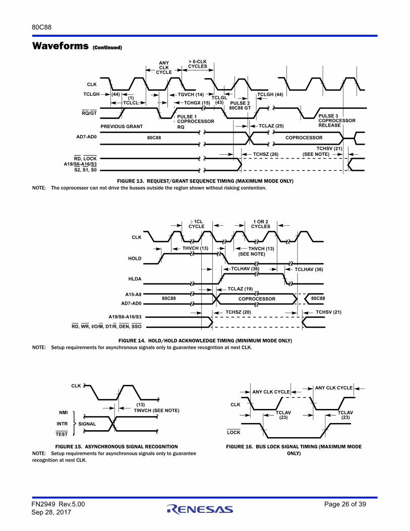
FIGURE 13. REQUEST/GRANT SEQUENCE TIMING (MAXIMUM MODE ONLY)NOTE: The coprocessor can not drive the busses outside the region shown without risking contention.
FIGURE 14. HOLD/HOLD ACKNOWLEDGE TIMING (MINIMUM MODE ONLY)NOTE: Setup requirements for asynchronous signals only to guarantee recognition at next CLK.
FIGURE 15. ASYNCHRONOUS SIGNAL RECOGNITIONNOTE: Setup requirements for asynchronous signals only to guarantee recognition at next CLK.
FIGURE 16. BUS LOCK SIGNAL TIMING (MAXIMUM MODEONLY)
Waveforms (Continued)
CLK
TCLGH
RQ/GT
PREVIOUS GRANT
AD7-AD0
RD, LOCKA19/S6-A16/S3
S2, S1, S0
TCLCL
ANYCLK
CYCLE
> 0-CLKCYCLES
PULSE 2
80C88
TGVCH (14)
TCHGX (15)
TCLGH (44)
PULSE 1COPROCESSORRQ TCLAZ (25)
80C88 GT
PULSE 3COPROCESSORRELEASE
(SEE NOTE)TCHSZ (26)
(1) TCLGL(43)
COPROCESSOR
TCHSV (21)
(44)
CLK
HOLD
HLDA
A15-A8
A19/S6-A16/S3
RD, WR, I/O/M, DT/R, DEN, SSO
80C88
THVCH (13)
TCLHAV (36)
1CL 1 OR 2CYCLES
TCLAZ (19)
COPROCESSOR 80C88
TCLHAV (36)
CYCLE
TCHSZ (20)
THVCH (13)
TCHSV (21)
(SEE NOTE)
AD7-AD0
NMI
INTR
TEST
CLK
SIGNAL
TINVCH (SEE NOTE)(13)
ANY CLK CYCLE
CLK
LOCK
TCLAV
ANY CLK CYCLE
(23)TCLAV
(23)
FN2949 Rev.5.00 Page 26 of 39Sep 28, 2017
80C88
AC Test Circuit AC Testing Input, Output Waveform
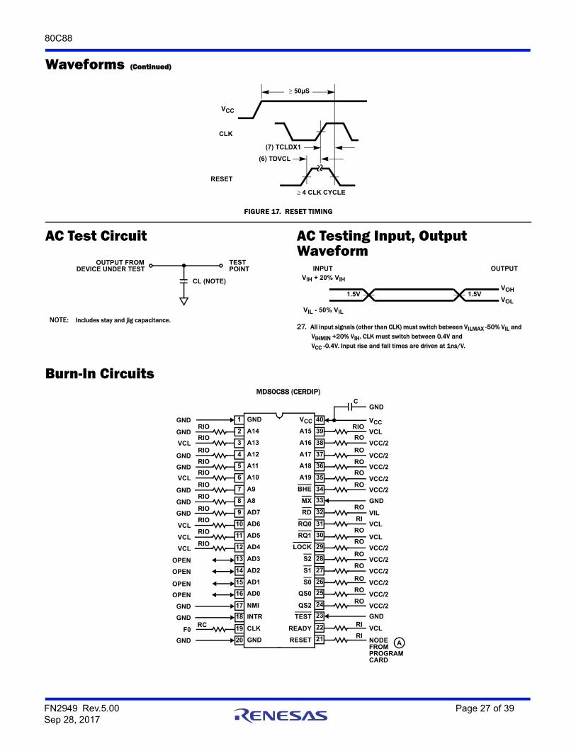
FIGURE 17. RESET TIMING
Waveforms (Continued)
VCC
CLK
RESET
50µS
4 CLK CYCLE
(7) TCLDX1
(6) TDVCL
OUTPUT FROMDEVICE UNDER TEST
TEST
CL (NOTE)
POINT
NOTE: Includes stay and jig capacitance.
INPUTVIH + 20% VIH
VIL - 50% VIL
OUTPUT
VOH
VOL1.5V 1.5V
27. All input signals (other than CLK) must switch between VILMAX -50% VIL and
VIHMIN +20% VIH. CLK must switch between 0.4V and
VCC -0.4V. Input rise and fall times are driven at 1ns/V.
Burn-In Circuits MD80C88 (CERDIP)
33
34
35
36
37
38
40
32
31
30
29
24
25
26
27
28
21
22
23
13
2
3
4
5
6
7
8
9
10
11
12
14
15
16
17
18
19
20
39
GND
GND
NMI
INTR
CLK
GND
1RIO
RIO
RIO
RIO
RIO
RIO
RIO
RIO
RIO
RIO
RIO
RC
RI
RI
VCC/2
VCL
VCL
VIL
GND
VCC/2
VCC/2
RI
VCC/2
VCC/2
VCC/2
VCL
VCC
GND
RIO
RO
RO
RO
VCC/2
VCC/2
VCC/2
VCC/2
VCC/2
GND
VCL
NODEFROMPROGRAMCARD
GND
GND
VCL
GND
GND
VCL
GND
GND
GND
VCL
VCL
VCL
OPEN
OPEN
OPEN
OPEN
GND
GND
F0
RO
RO
RO
RO
RO
RO
RO
RO
RO
RO
A
A14
A13
A12
A11
A10
A9
A8
AD7
AD6
AD5
AD4
AD3
AD2
AD1
AD0
VCC
QS2
TEST
READY
RESET
A15
A16
A17
A18
A19
BHE
MX
RD
RQ0
RQ1
LOCK
S2
S1
S0
QS0
C
FN2949 Rev.5.00 Page 27 of 39Sep 28, 2017

80C88
Die CharacteristicsMETALLIZATION:
Type: Silicon - AluminumThickness: 11KÅ 2kÅ
GLASSIVATION:Type: SiO2Thickness: 8kÅ 1kÅ
WORST CASE CURRENT DENSITY:1.5 x 10⁵ A/cm2
Burn-In Circuits (Continued)
COMPONENTS:
1. RI = 10kΩ 5%, 1/4W
2. RO = 1.2kΩ ±5%, 1/4W
3. RIO = 2.7kΩ ±5%, 1/4W
4. RC = 1kΩ ±5%, 1/4W
5. C = 0.01µF (Minimum)
NOTES:
1. VCC = 5.5V 0.5V, GND = 0V.
2. Input voltage limits (except clock):VIL (Maximum) = 0.4VVIH (Minimum) = 2.6V, VIH (Clock) = VCC - 0.4V) minimum.
3. VCC/2 is external supply set to 2.7V 10%.
4. VCL is generated on program card (VCC - 0.65V).
5. Pins 13 - 16 input sequenced instructions from internal hold devices, (DIP Only).
6. F0 = 100kHz 10%.
7. Node = a 40s pulse every 2.56ms.A
FN2949 Rev.5.00 Page 28 of 39Sep 28, 2017

80C88
Metallization Mask Layout80C88
A11 A12 A13 A14 A17/S4 A18/S5GND A16/S3VCC A15
A19/S6
SSO
MN/MX
RD
A10
A9
A8
AD7
AD6
AD5
AD4
AD3
AD2
AD1
AD0
NMI INTR CLK GND RESET READY TEST ALE DEN
HOLD
HLDA
WR
IO/M
DT/R
INTA
FN2949 Rev.5.00 Page 29 of 39Sep 28, 2017

80C88
Instruction Set Summary
MNEMONIC AND DESCRIPTION
INSTRUCTION CODE
7 6 5 4 3 2 1 0 7 6 5 4 3 2 1 0 7 6 5 4 3 2 1 0 7 6 5 4 3 2 1 0
DATA TRANSFERMOV = MOVE:
Register/Memory to/from Register
1 0 0 0 1 0 d w mod reg r/m
Immediate to Register/Memory
1 1 0 0 0 1 1 w mod 0 0 0 r/m data data if w 1
Immediate to Register 1 0 1 1 w reg data data if w 1
Memory to Accumulator 1 0 1 0 0 0 0 w addr-low addr-high
Accumulator to Memory 1 0 1 0 0 0 1 w addr-low addr-high
Register/Memory to Segment Register ††
1 0 0 0 1 1 1 0 mod 0 reg r/m
Segment Register to Register/Memory
1 0 0 0 1 1 0 0 mod 0 reg r/m
PUSH = Push:
Register/Memory 1 1 1 1 1 1 1 1 mod 1 1 0 r/m
Register 0 1 0 1 0 reg
Segment Register 0 0 0 reg 1 1 0
POP = Pop:
Register/Memory 1 0 0 0 1 1 1 1 mod 0 0 0 r/m
Register 0 1 0 1 1 reg
Segment Register 0 0 0 reg 1 1 1
XCHG = Exchange:
Register/Memory with Register
1 0 0 0 0 1 1 w mod reg r/m
Register with Accumulator 1 0 0 1 0 reg
IN = Input from:
Fixed Port 1 1 1 0 0 1 0 w port
Variable Port 1 1 1 0 1 1 0 w
OUT = Output to:
Fixed Port 1 1 1 0 0 1 1 w port
Variable Port 1 1 1 0 1 1 1 w
XLAT = Translate Byte to AL 1 1 0 1 0 1 1 1
LEA = Load EA to Register2 1 0 0 0 1 1 0 1 mod reg r/m
LDS = Load Pointer to DS 1 1 0 0 0 1 0 1 mod reg r/m
LES = Load Pointer to ES 1 1 0 0 0 1 0 0 mod reg r/m
LAHF = Load AH with Flags 1 0 0 1 1 1 1 1
SAHF = Store AH into Flags 1 0 0 1 1 1 1 0
PUSHF = Push Flags 1 0 0 1 1 1 0 0
POPF = Pop Flags 1 0 0 1 1 1 0 1
FN2949 Rev.5.00 Page 30 of 39Sep 28, 2017
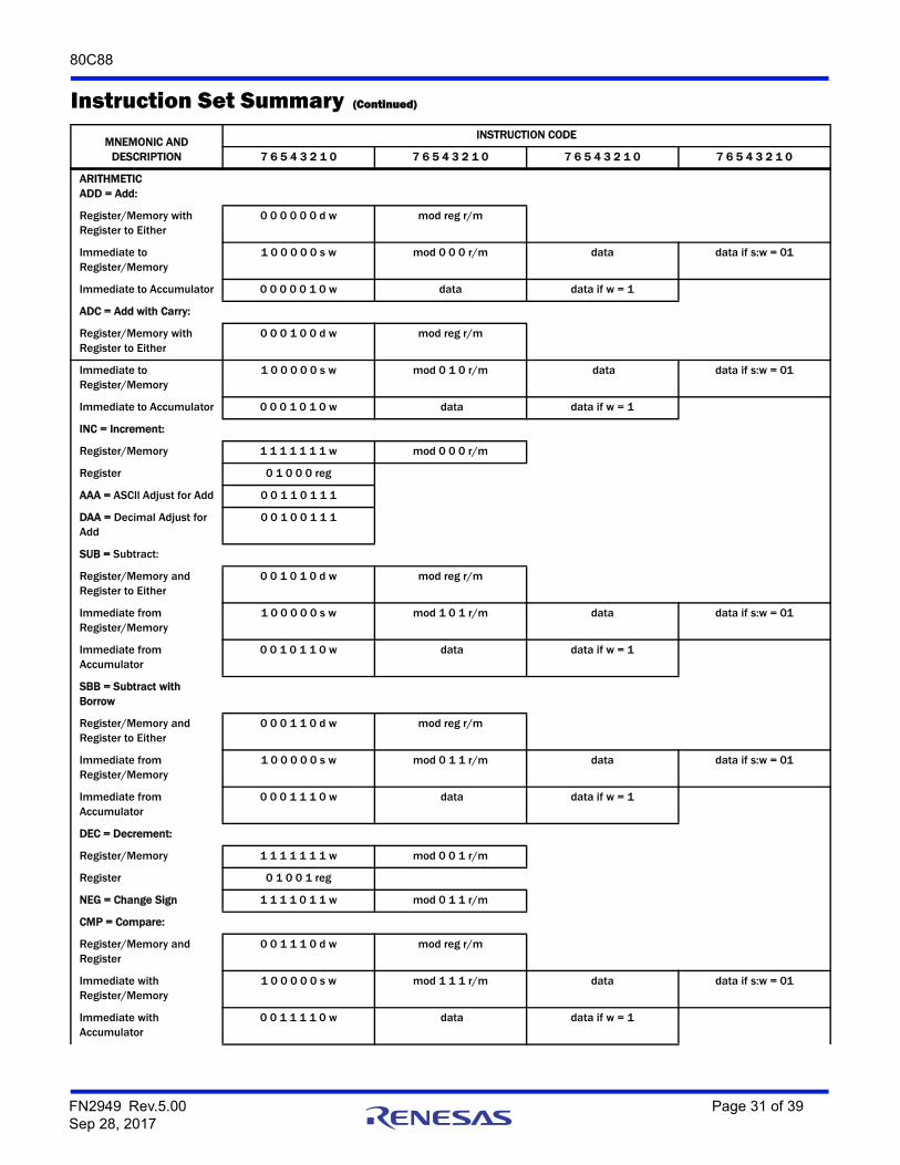
80C88
ARITHMETICADD = Add:
Register/Memory with Register to Either
0 0 0 0 0 0 d w mod reg r/m
Immediate to Register/Memory
1 0 0 0 0 0 s w mod 0 0 0 r/m data data if s:w = 01
Immediate to Accumulator 0 0 0 0 0 1 0 w data data if w = 1
ADC = Add with Carry:
Register/Memory with Register to Either
0 0 0 1 0 0 d w mod reg r/m
Immediate to Register/Memory
1 0 0 0 0 0 s w mod 0 1 0 r/m data data if s:w = 01
Immediate to Accumulator 0 0 0 1 0 1 0 w data data if w = 1
INC = Increment:
Register/Memory 1 1 1 1 1 1 1 w mod 0 0 0 r/m
Register 0 1 0 0 0 reg
AAA = ASCll Adjust for Add 0 0 1 1 0 1 1 1
DAA = Decimal Adjust for Add
0 0 1 0 0 1 1 1
SUB = Subtract:
Register/Memory and Register to Either
0 0 1 0 1 0 d w mod reg r/m
Immediate from Register/Memory
1 0 0 0 0 0 s w mod 1 0 1 r/m data data if s:w = 01
Immediate from Accumulator
0 0 1 0 1 1 0 w data data if w = 1
SBB = Subtract with Borrow
Register/Memory and Register to Either
0 0 0 1 1 0 d w mod reg r/m
Immediate from Register/Memory
1 0 0 0 0 0 s w mod 0 1 1 r/m data data if s:w = 01
Immediate from Accumulator
0 0 0 1 1 1 0 w data data if w = 1
DEC = Decrement:
Register/Memory 1 1 1 1 1 1 1 w mod 0 0 1 r/m
Register 0 1 0 0 1 reg
NEG = Change Sign 1 1 1 1 0 1 1 w mod 0 1 1 r/m
CMP = Compare:
Register/Memory and Register
0 0 1 1 1 0 d w mod reg r/m
Immediate with Register/Memory
1 0 0 0 0 0 s w mod 1 1 1 r/m data data if s:w = 01
Immediate with Accumulator
0 0 1 1 1 1 0 w data data if w = 1
Instruction Set Summary (Continued)
MNEMONIC AND DESCRIPTION
INSTRUCTION CODE
7 6 5 4 3 2 1 0 7 6 5 4 3 2 1 0 7 6 5 4 3 2 1 0 7 6 5 4 3 2 1 0
FN2949 Rev.5.00 Page 31 of 39Sep 28, 2017

80C88
AAS = ASCll Adjust for Subtract
0 0 1 1 1 1 1 1
DAS = Decimal Adjust for Subtract
0 0 1 0 1 1 1 1
MUL = Multiply (Unsigned) 1 1 1 1 0 1 1 w mod 1 0 0 r/m
IMUL = Integer Multiply (Signed)
1 1 1 1 0 1 1 w mod 1 0 1 r/m
AAM = ASCll Adjust for Multiply
1 1 0 1 0 1 0 0 0 0 0 0 1 0 1 0
DlV = Divide (Unsigned) 1 1 1 1 0 1 1 w mod 1 1 0 r/m
IDlV = Integer Divide (Signed)
1 1 1 1 0 1 1 w mod 1 1 1 r/m
AAD = ASClI Adjust for Divide
1 1 0 1 0 1 0 1 0 0 0 0 1 0 1 0
CBW = Convert Byte to Word
1 0 0 1 1 0 0 0
CWD = Convert Word to Double Word
1 0 0 1 1 0 0 1
LOGIC
NOT = Invert 1 1 1 1 0 1 1 w mod 0 1 0 r/m
SHL/SAL = Shift Logical/Arithmetic Left
1 1 0 1 0 0 v w mod 1 0 0 r/m
SHR = Shift Logical Right 1 1 0 1 0 0 v w mod 1 0 1 r/m
SAR = Shift Arithmetic Right
1 1 0 1 0 0 v w mod 1 1 1 r/m
ROL = Rotate Left 1 1 0 1 0 0 v w mod 0 0 0 r/m
ROR = Rotate Right 1 1 0 1 0 0 v w mod 0 0 1 r/m
RCL = Rotate Through Carry Flag Left
1 1 0 1 0 0 v w mod 0 1 0 r/m
RCR = Rotate Through Carry Right
1 1 0 1 0 0 v w mod 0 1 1 r/m
AND = And:
Reg./Memory and Register to Either
0 0 1 0 0 0 0 d w mod reg r/m
Immediate to Register/Memory
1 0 0 0 0 0 0 w mod 1 0 0 r/m data data if w = 1
Immediate to Accumulator 0 0 1 0 0 1 0 w data data if w = 1
TEST = And Function to Flags, No Result:
Register/Memory and Register
1 0 0 0 0 1 0 w mod reg r/m
Immediate Data and Register/Memory
1 1 1 1 0 1 1 w mod 0 0 0 r/m data data if w = 1
Immediate Data and Accumulator
1 0 1 0 1 0 0 w data data if w = 1
Instruction Set Summary (Continued)
MNEMONIC AND DESCRIPTION
INSTRUCTION CODE
7 6 5 4 3 2 1 0 7 6 5 4 3 2 1 0 7 6 5 4 3 2 1 0 7 6 5 4 3 2 1 0
FN2949 Rev.5.00 Page 32 of 39Sep 28, 2017

80C88
OR = Or:
Register/Memory and Register to Either
0 0 0 0 1 0 d w mod reg r/m
Immediate to Register/Memory
1 0 0 0 0 0 0 w mod 1 0 1 r/m data data if w = 1
Immediate to Accumulator 0 0 0 0 1 1 0 w data data if w = 1
XOR = Exclusive or:
Register/Memory and Register to Either
0 0 1 1 0 0 d w mod reg r/m
Immediate to Register/Memory
1 0 0 0 0 0 0 w mod 1 1 0 r/m data data if w = 1
Immediate to Accumulator 0 0 1 1 0 1 0 w data data if w = 1
STRING MANIPULATION
REP = Repeat 1 1 1 1 0 0 1 z
MOVS = Move Byte/Word 1 0 1 0 0 1 0 w
CMPS = Compare Byte/Word
1 0 1 0 0 1 1 w
SCAS = Scan Byte/Word 1 0 1 0 1 1 1 w
LODS = Load Byte/Word to AL/AX
1 0 1 0 1 1 0 w
STOS = Stor Byte/Word from AL/A
1 0 1 0 1 0 1 w
CONTROL TRANSFER
CALL = Call:
Direct Within Segment 1 1 1 0 1 0 0 0 disp-low disp-high
Indirect Within Segment 1 1 1 1 1 1 1 1 mod 0 1 0 r/m
Direct Intersegment 1 0 0 1 1 0 1 0 offset-low offset-high
seg-low seg-high
Indirect Intersegment 1 1 1 1 1 1 1 1 mod 0 1 1 r/m
JMP = Unconditional Jump:
Direct Within Segment 1 1 1 0 1 0 0 1 disp-low disp-high
Direct Within Segment-Short
1 1 1 0 1 0 1 1 disp
Indirect Within Segment 1 1 1 1 1 1 1 1 mod 1 0 0 r/m
Direct Intersegment 1 1 1 0 1 0 1 0 offset-low offset-high
seg-low seg-high
Indirect Intersegment 1 1 1 1 1 1 1 1 mod 1 0 1 r/m
RET = Return from CALL:
Within Segment 1 1 0 0 0 0 1 1
Within Seg Adding lmmed to SP
1 1 0 0 0 0 1 0 data-low data-high
Intersegment 1 1 0 0 1 0 1 1
Instruction Set Summary (Continued)
MNEMONIC AND DESCRIPTION
INSTRUCTION CODE
7 6 5 4 3 2 1 0 7 6 5 4 3 2 1 0 7 6 5 4 3 2 1 0 7 6 5 4 3 2 1 0
FN2949 Rev.5.00 Page 33 of 39Sep 28, 2017

80C88
Intersegment Adding Immediate to SP
1 1 0 0 1 0 1 0 data-low data-high
JE/JZ = Jump on Equal/Zero
0 1 1 1 0 1 0 0 disp
JL/JNGE = Jump on Less/Not Greater or Equal
0 1 1 1 1 1 0 0 disp
JLE/JNG = Jump on Less or Equal/ Not Greater
0 1 1 1 1 1 1 0 disp
JB/JNAE = Jump on Below/Not Above or Equal
0 1 1 1 0 0 1 0 disp
JBE/JNA = Jump on Below or Equal/Not Above
0 1 1 1 0 1 1 0 disp
JP/JPE = Jump on Parity/Parity Even
0 1 1 1 1 0 1 0 disp
JO = Jump on Overflow 0 1 1 1 0 0 0 0 disp
JS = Jump on Sign 0 1 1 1 1 0 0 0 disp
JNE/JNZ = Jump on Not Equal/Not Zero
0 1 1 1 0 1 0 1 disp
JNL/JGE = Jump on Not Less/Greater or Equal
0 1 1 1 1 1 0 1 disp
JNLE/JG = Jump on Not Less or Equal/Greater
0 1 1 1 1 1 1 1 disp
JNB/JAE = Jump on Not Below/Above or Equal
0 1 1 1 0 0 1 1 disp
JNBE/JA = Jump on Not Below or Equal/Above
0 1 1 1 0 1 1 1 disp
JNP/JPO = Jump on Not Par/Par Odd
0 1 1 1 1 0 1 1 disp
JNO = Jump on Not Overflow
0 1 1 1 0 0 0 1 disp
JNS = Jump on Not Sign 0 1 1 1 1 0 0 1 disp
LOOP = Loop CX Times 1 1 1 0 0 0 1 0 disp
LOOPZ/LOOPE = Loop While Zero/Equal
1 1 1 0 0 0 0 1 disp
LOOPNZ/LOOPNE = Loop While Not Zero/Equal
1 1 1 0 0 0 0 0 disp
JCXZ = Jump on CX Zero 1 1 1 0 0 0 1 1 disp
INT = Interrupt
Type Specified 1 1 0 0 1 1 0 1 type
Type 3 1 1 0 0 1 1 0 0
INTO = Interrupt on Overflow
1 1 0 0 1 1 1 0
IRET = Interrupt Return 1 1 0 0 1 1 1 1
Instruction Set Summary (Continued)
MNEMONIC AND DESCRIPTION
INSTRUCTION CODE
7 6 5 4 3 2 1 0 7 6 5 4 3 2 1 0 7 6 5 4 3 2 1 0 7 6 5 4 3 2 1 0
FN2949 Rev.5.00 Page 34 of 39Sep 28, 2017

80C88
PROCESSOR CONTROL
CLC = Clear Carry 1 1 1 1 1 0 0 0
CMC = Complement Carry 1 1 1 1 0 1 0 1
STC = Set Carry 1 1 1 1 1 0 0 1
CLD = Clear Direction 1 1 1 1 1 1 0 0
STD = Set Direction 1 1 1 1 1 1 0 1
CLl = Clear Interrupt 1 1 1 1 1 0 1 0
ST = Set Interrupt 1 1 1 1 1 0 1 1
HLT = Halt 1 1 1 1 0 1 0 0
WAIT = Wait 1 0 0 1 1 0 1 1
ESC = Escape (to External Device)
1 1 0 1 1 x x x mod x x x r/m
LOCK = Bus Lock Prefix 1 1 1 1 0 0 0 0
Instruction Set Summary (Continued)
MNEMONIC AND DESCRIPTION
INSTRUCTION CODE
7 6 5 4 3 2 1 0 7 6 5 4 3 2 1 0 7 6 5 4 3 2 1 0 7 6 5 4 3 2 1 0
FN2949 Rev.5.00 Page 35 of 39Sep 28, 2017

80C88
NOTES:
AL = 8-bit accumulatorAX = 16-bit accumulatorCX = Count registerDS= Data segmentES = Extra segmentAbove/below refers to unsigned value.Greater = more positive;Less = less positive (more negative) signed valuesif d = 1 then “to” reg; if d = 0 then “from” regif w = 1 then word instruction; if w = 0 then byte
instructionif mod = 11 then r/m is treated as a REG fieldif mod = 00 then DISP = 0†, disp-low and disp-high
are absentif mod = 01 then DISP = disp-low sign-extended
16-bits, disp-high is absentif mod = 10 then DISP = disp-high:disp-lowif r/m = 000 then EA = (BX) + (SI) + DISPif r/m = 001 then EA = (BX) + (DI) + DISPif r/m = 010 then EA = (BP) + (SI) + DISPif r/m = 011 then EA = (BP) + (DI) + DISPif r/m = 100 then EA = (SI) + DISPif r/m = 101 then EA = (DI) + DISPif r/m = 110 then EA = (BP) + DISP †if r/m = 111 then EA = (BX) + DISPDISP follows 2nd byte of instruction (before data
if required)† except if mod = 00 and r/m = 110 then
EA = disp-high: disp-low.†† MOV CS, REG/MEMORY not allowed.
if s:w = 01 then 16-bits of immediate data form the operand.if s:w = 11 then an immediate data byte is sign extended
to form the 16-bit operand.if v = 0 then “count” = 1; if v = 1 then “count” in (CL)x = don't carez is used for string primitives for comparison with ZF FLAG.
SEGMENT OVERRIDE PREFIX
001 reg 11 0
REG is assigned according to the following table:
16-BIT (w = 1) 8-BIT (w = 0) SEGMENT
000 AX 000 AL 00 ES
001 CX 001 CL 01 CS
010 DX 010 DL 10 SS
011 BX 011 BL 11 DS
100 SP 100 AH
101 BP 101 CH
110 SI 110 DH
111 DI 111 BH
Instructions which reference the flag register file as a 16-bit object use the symbol FLAGS to represent the file:
FLAGS =
X:X:X:X:(OF):(DF):(IF):(TF):(SF):(ZF):X:(AF):X:(PF):X:(CF)
Mnemonics Intel, 1978
Instruction Set Summary (Continued)
MNEMONIC AND DESCRIPTION
INSTRUCTION CODE
7 6 5 4 3 2 1 0 7 6 5 4 3 2 1 0 7 6 5 4 3 2 1 0 7 6 5 4 3 2 1 0
FN2949 Rev.5.00 Page 36 of 39Sep 28, 2017

80C88
Intersil products are manufactured, assembled and tested utilizing ISO9001 quality systems as notedin the quality certifications found at www.intersil.com/en/support/qualandreliability.html
Intersil products are sold by description only. Intersil may modify the circuit design and/or specifications of products at any time without notice, provided that such modification does not, in Intersil's sole judgment, affect the form, fit or function of the product. Accordingly, the reader is cautioned to verify that datasheets are current before placing orders. Information furnished by Intersil is believed to be accurate and reliable. However, no responsibility is assumed by Intersil or its subsidiaries for its use; nor for any infringements of patents or other rights of third parties which may result from its use. No license is granted by implication or otherwise under any patent or patent rights of Intersil or its subsidiaries.
For information regarding Intersil Corporation and its products, see www.intersil.com
For additional products, see www.intersil.com/en/products.html
© Copyright Intersil Americas LLC 2002-2017. All Rights Reserved.All trademarks and registered trademarks are the property of their respective owners.
About IntersilIntersil Corporation is a leading provider of innovative power management and precision analog solutions. The company's products address some of the largest markets within the industrial and infrastructure, mobile computing, and high-end consumer markets.For the most updated datasheet, application notes, related documentation, and related parts, see the respective product information page found at www.intersil.com. For a listing of definitions and abbreviations of common terms used in our documents, visit www.intersil.com/glossary.You can report errors or suggestions for improving this datasheet by visiting www.intersil.com/ask.Reliability reports are also available from our website at www.intersil.com/support.
Revision History The revision history provided is for informational purposes only and is believed to be accurate, but not warranted. Please visit our website to make sure you have the latest revision.
DATE REVISION CHANGE
Sep 28, 2017 FN2949.5 Added Related Literature section.Updated Ordering Information table.Applied Intersil A Renesas Company template.
FN2949 Rev.5.00 Page 37 of 39Sep 28, 2017
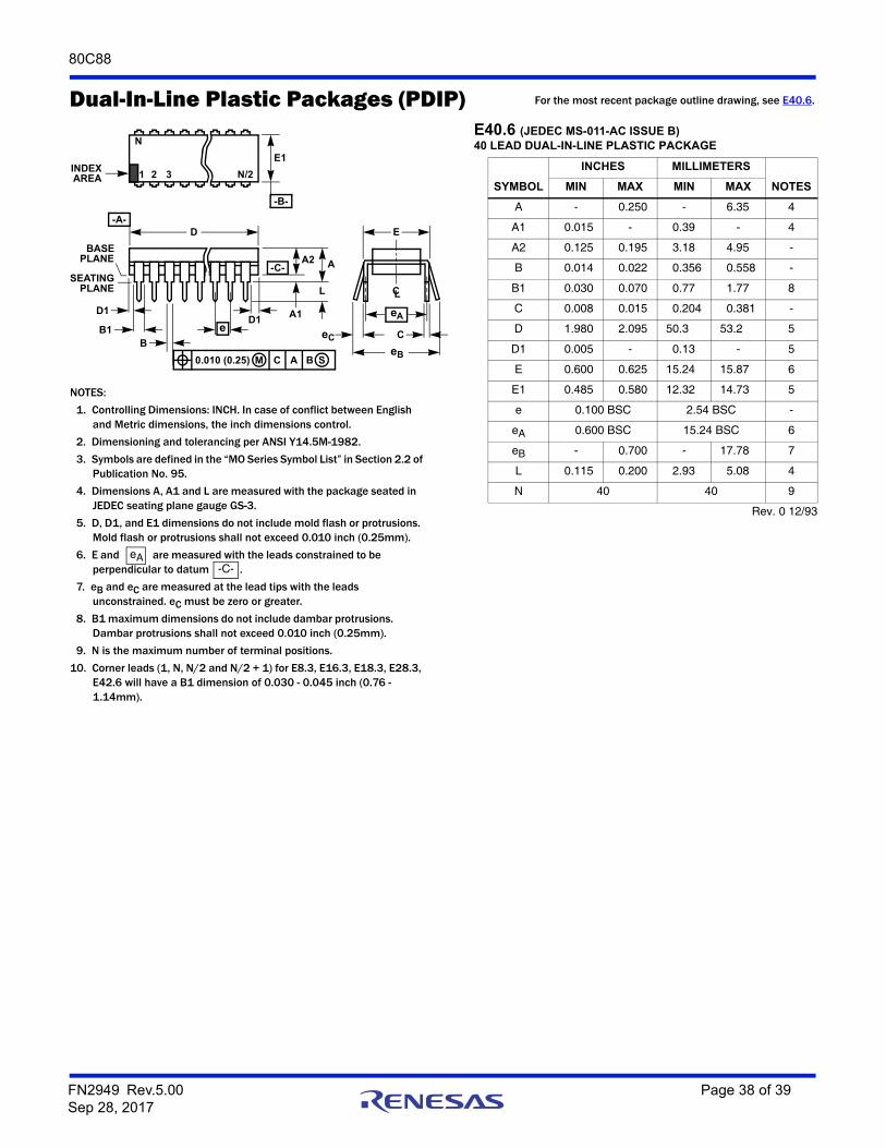
80C88
FN2949 Rev.5.00 Page 38 of 39Sep 28, 2017
Dual-In-Line Plastic Packages (PDIP)
NOTES:
1. Controlling Dimensions: INCH. In case of conflict between English and Metric dimensions, the inch dimensions control.
2. Dimensioning and tolerancing per ANSI Y14.5M-1982.
3. Symbols are defined in the “MO Series Symbol List” in Section 2.2 of Publication No. 95.
4. Dimensions A, A1 and L are measured with the package seated in JEDEC seating plane gauge GS-3.
5. D, D1, and E1 dimensions do not include mold flash or protrusions. Mold flash or protrusions shall not exceed 0.010 inch (0.25mm).
6. E and are measured with the leads constrained to be perpendicular to datum .
7. eB and eC are measured at the lead tips with the leads unconstrained. eC must be zero or greater.
8. B1 maximum dimensions do not include dambar protrusions. Dambar protrusions shall not exceed 0.010 inch (0.25mm).
9. N is the maximum number of terminal positions.
10. Corner leads (1, N, N/2 and N/2 + 1) for E8.3, E16.3, E18.3, E28.3, E42.6 will have a B1 dimension of 0.030 - 0.045 inch (0.76 - 1.14mm).
eA-C-
CL
E
eA
C
eB
eC
-B-
E1INDEX
1 2 3 N/2
N
AREA
SEATING
BASEPLANE
PLANE
-C-
D1
B1B
e
D
D1
AA2
L
A1
-A-
0.010 (0.25) C AM B S
E40.6 (JEDEC MS-011-AC ISSUE B)40 LEAD DUAL-IN-LINE PLASTIC PACKAGE
SYMBOL
INCHES MILLIMETERS
NOTESMIN MAX MIN MAX
A - 0.250 - 6.35 4
A1 0.015 - 0.39 - 4
A2 0.125 0.195 3.18 4.95 -
B 0.014 0.022 0.356 0.558 -
B1 0.030 0.070 0.77 1.77 8
C 0.008 0.015 0.204 0.381 -
D 1.980 2.095 50.3 53.2 5
D1 0.005 - 0.13 - 5
E 0.600 0.625 15.24 15.87 6
E1 0.485 0.580 12.32 14.73 5
e 0.100 BSC 2.54 BSC -
eA 0.600 BSC 15.24 BSC 6
eB - 0.700 - 17.78 7
L 0.115 0.200 2.93 5.08 4
N 40 40 9
Rev. 0 12/93
For the most recent package outline drawing, see E40.6.

80C88
FN2949 Rev.5.00 Page 39 of 39Sep 28, 2017
Ceramic Dual-In-Line Frit Seal Packages (CERDIP)
NOTES:
1. Index area: A notch or a pin one identification mark shall be located adjacent to pin one and shall be located within the shaded area shown. The manufacturer’s identification shall not be used as a pin one identification mark.
2. The maximum limits of lead dimensions b and c or M shall be measured at the centroid of the finished lead surfaces, when solder dip or tin plate lead finish is applied.
3. Dimensions b1 and c1 apply to lead base metal only. Dimension M applies to lead plating and finish thickness.
4. Corner leads (1, N, N/2, and N/2+1) can be configured with a partial lead paddle. For this configuration dimension b3 replaces dimension b2.
5. This dimension allows for off-center lid, meniscus, and glass overrun.
6. Dimension Q shall be measured from the seating plane to the base plane.
7. Measure dimension S1 at all four corners.
8. N is the maximum number of terminal positions.
9. Dimensioning and tolerancing per ANSI Y14.5M - 1982.
10. Controlling dimension: INCH.
bbb C A - BS
c
Q
L
ASEATING
BASE
D
PLANE
PLANE
-D--A-
-C-
-B-
D
E
S1
b2
b
A
e
M
c1
b1
(c)
(b)
SECTION A-A
BASE
LEAD FINISH
METAL
eA/2
A
M
S S
ccc C A - BM DS S aaa C A - BM DS S
eA
F40.6 MIL-STD-1835 GDIP1-T40 (D-5, CONFIGURATION A)40 LEAD CERAMIC DUAL-IN-LINE FRIT SEAL PACKAGE
SYMBOL
INCHES MILLIMETERS
NOTESMIN MAX MIN MAX
A - 0.225 - 5.72 -
b 0.014 0.026 0.36 0.66 2
b1 0.014 0.023 0.36 0.58 3
b2 0.045 0.065 1.14 1.65 -
b3 0.023 0.045 0.58 1.14 4
c 0.008 0.018 0.20 0.46 2
c1 0.008 0.015 0.20 0.38 3
D - 2.096 - 53.24 5
E 0.510 0.620 12.95 15.75 5
e 0.100 BSC 2.54 BSC -
eA 0.600 BSC 15.24 BSC -
eA/2 0.300 BSC 7.62 BSC -
L 0.125 0.200 3.18 5.08 -
Q 0.015 0.070 0.38 1.78 6
S1 0.005 - 0.13 - 7
90o 105o 90o 105o -
aaa - 0.015 - 0.38 -
bbb - 0.030 - 0.76 -
ccc - 0.010 - 0.25 -
M - 0.0015 - 0.038 2, 3
N 40 40 8
Rev. 0 4/94
For the most recent package outline drawing, see F40.6.