datasheet - stwbc2-hp - digital controller for wireless
TRANSCRIPT

Features• Digital controller for Qi certified wireless power transmitters
– Compliant with WPC 1.3– Power Class 0 BPP (5 W) and EPP (15 W)– Power Tx design topologies MP-A2 and MP-A22– Proprietary ST Super Charge extension for high power charging
• SiP with uC and front end device:– ARM 32-bit Cortex™-M0+ CPU, frequency up to 64 MHz– 3x half-bridge drivers– Embedded 3.6 V / 5 V DC-DC– 3.3 V and 1.8 V LDOs– 6 V to 9 V voltage doubler– Qi FSK programmable modulator– Integrated current, voltage and phase demodulators– Integrated current and voltage sensors.
• Support for half- and full-bridge topologies with input DC-DC– Single and multi-coil topologies– Support for limited power sources such as 5 V 500 mA USB
• VIN operative range: 4.1 V to 24 V• USB physical interfaces
– USB power delivery• Communication interfaces
– UART– SPI (up to 28 Mbit/s)– I2C (up to 1 Mbit/s)– Up to 8x GPIOs
• Peripherals– 8-channel 12-bit 0.5 us ADC– Low side differential current sensor– Q-Factor driver
• Memory– 128 Kbytes of Flash memory with ECC– 32 Kbytes of SRAM with HW parity check
• Development support: serial wire debug (SWD)• Operating temperature: -40°C up to 125°C.• Package: VFQFPN68L 8x8 mm pitch 0.4• 96-bit unique ID
DescriptionThe STWBC2 -HP is a digital controller specifically dedicated to design Qi-certifiedWireless Power TX applications. The STWBC2-HP is a SiP including an STM32™microcontroller and an application-specific front-end die.
Product status link
STWBC2 -HP
Product label
Table 1. Ordering information
Order code Package Packaging
STWBC2-HP VFQFPN68 Tape & Reel
Digital controller for wireless battery charger transmitters
STWBC2-HP
Datasheet
DS13825 - Rev 1.0 - September 2021For further information contact your local STMicroelectronics sales office.
www.st.com

Specifically, the STM32™ microcontroller embedded into the STWBC2-HP is theSTM32G071.
The STWBC2-HP is capable of driving the DC-DC stage and the half- or full-bridgeinverter stage of a generic Qi wireless battery charging TX. It generates andcontrols the relevant PWM signals by means of a PWM machine capable of 1.47ns resolution. In order to achieve that, the front-end die includes a 40 MHz PLL and a17-step DLL.
The STWBC2-HP front end is capable of working from any DC voltage in the range of4.1 V to 24 V and embeds:• 3x half-bridge drivers capable of driving both the FB inverter or the DC-DC
MOSFET• 2x PWM outputs for external gate drivers• 2x LED / speaker drivers• 3.6 V / 5 V monolithic buck DC-DC to supply the analog portion of the die• 3.3 V LDO to supply the STM32• 1.8 V LDO to supply the core• 6 V to 9 V voltage doubler to supply the gate drivers• Resonant tank current, voltage and phase sense circuitry and Q-factor driver• USB D+/D- external interface pins for USB PD
The Front End die also includes specific registers and an SPI interface with theSTM32, in combination with an output mux for analog signals to the STM32 ADC,and GPIOs for digital signals to the STM32 core.
The STM32 microcontroller embeds an ARM Cortex™-M0+ CPU with up to 128 kFlash memory and up to 32 k of SRAM with parity check, with a clock frequency upto 64 MHz. It also embeds a 12-bit, 0.5 μs ADC and provides UART, I2C, SPI andGPIOs
The STM32G071 embedded in STWBC2-HP also provides two 12-bit DACs andUSB-PD controller.
STWBC2-HP
DS13825 - Rev 1.0 page 2/96

1 Block diagrams
1.1 STWBC2-HP architectureThe following image illustrates the overall system blocks implemented in the STWBC2-HP architecture.The STWBC2-HP is a system-in-package combining an STM32G071 MCU die with a Wireless Power specific diewhich integrates several application-specific functions.The STWBC2-HP supports both half-bridge and full-bridge coil driver topologies, together with a digital DC-DCcontroller, which regulates the input voltage of the bridge in order to control the amount of power transmitted tothe receiver.The digital controller also regulates the inverter operating frequency and duty cycle to further adjust the amount ofpower increasing the overall efficiency at light load.It implements the WPC Qi protocol, including Foreign Object Detection (FOD) extensions. An accurate Q-factormeasurement provides enhanced FOD.The STWBC2-HP is able to manage both WPC Baseline Power Profile (up to 5 W) and Extended Power Profile(EPP).
Figure 1. STWBC2-HP device architecture
STWBC2-HP Block diagrams
DS13825 - Rev 1.0 page 3/96

1.2 Typical application
1.2.1 Qi single coil, fixed frequency full-bridge, USB powered
Figure 2. Qi single coil, fixed frequency full-bridge, USB powered
STWBC2-HP Typical application
DS13825 - Rev 1.0 page 4/96

1.2.2 Qi single coil, variable frequency full-bridge, USB powered
Figure 3. Qi single coil, variable frequency full-bridge, USB powered
STWBC2-HP Typical application
DS13825 - Rev 1.0 page 5/96

2 Analog Front-End (AFE)
The following figure shows a simplified block diagram of STWBC2-HP AFE.
Figure 4. STWBC2-HP AFE block diagram
2.1 Analog AFE functions
2.1.1 Power managementThe figure below shows the block diagram of the STWBC2-HP power management. The power management ofthe whole system is fully integrated in STWBC2-HP AFE. Power supply for µC (STM32G071) is provided by LDO3V3.The power source of the STWBC2-HP application is a DC voltage. In industrial applications it is generally asimple DC source up to VIN=24 V. In consumer applications most power sources are interfaced using µUSB orUSB-C connector, therefore the STWBC2-HP is designed to support current-limited supplies operating down to4.1 V. The STWBC2-HP is able to negotiate power contract with USB-C signaling or using USB Power Deliveryprotocol.STWBC2-HP generates its own power supplies from the power source directly and with good efficiency: to obtainthis result a DC-DC BUCK converter is integrated into the STWBC2-HP.
STWBC2-HP Analog Front-End (AFE)
DS13825 - Rev 1.0 page 6/96

Figure 5. Power management
The on-board DC-DC BUCK converter provides VDD supply voltage starting from external VIN DC source. VDDvoltage is available on the external pin and supplies the internal voltage regulators LDO 3V3 and LDO 1V8. Bothoutputs of these regulators are available on the external pin as shown in Figure 5.LDO 3V3 provides supply voltage for STM32G071 (internal bonding connection), for analog low-voltage circuitson STWBC2-HP AFE and finally for the level shift stages (from 1.8 V up to 3.3 V) used to interface digital signalbetween the STWBC2-HP (1.8 V digital domain) and the STM32G071 (3.3 V digital domain).LDO 1V8 provides supply voltage for STWBC2-HP AFE digital core and for input stage of the level shifter blocksmentioned before.
2.1.2 Reset strategyThe STWBC2-HP includes a single NRST pin that is star-connected to both AFE and STM32G071; both STM32and AFE use bi-directional pad for NRST. The following figure shows the simplified schematic of NRST functionimplementation.For STM32G071 the NRST pin function is:• Reset input• Warm reset output from WDG, SW reset, …
For AFE the NRST pin function is:• Reset input• Power ON Reset in link with BUCK DC-DC startup and LDOs startup.
STWBC2-HP Analog AFE functions
DS13825 - Rev 1.0 page 7/96

Figure 6. Reset strategy
The NRST pin electrical specifications are described in Section 3.5 .System reset filter is typically 440 ns.
2.1.3 Buck Boost DC-DC analog sectionThe DC-DC BUCK-BOOST converter provides power to the bridge which drives the wireless charging coil;this operation is done by using external power MOS driven by internal gate drivers. DC-DC BUCK-BOOST(hereinafter named BB-DCDC) is based on digital controller: the digital machine drives the gate drivers and useslow complexity analog circuits. Several different topologies can be implemented as shown by the following figures(LS=Low-Side driver, HS=High-Side driver):
Figure 7. Boost topologies
Figure 8. Buck topologies
STWBC2-HP Analog AFE functions
DS13825 - Rev 1.0 page 8/96

Figure 9. Buck/boost topologies
The BB-DCDC controller (see 2.1.3 Buck Boost DC-DC analog section) requires the following circuit from analogdomain:
Figure 10. BB DC-DC analog section
2.1.4 Analog monitorsThe STWBC2-HP AFE integrates 3 analog mux that are connected to STM32G071 die ADC inputs. Each muxselects a signal provided by an analog monitor cell. The mux switch time is fast enough allowing high speedconversion time from STM32 die.3 multiplexers are in use:• ADC0: this is the mux used for general purpose measurements• ADC1: this mux is either used as general purpose or to provide the voltage demodulation analog form.• ADC2: this mux is either used as general purpose or to provide the current demodulation analog form.
The channel selection (Sel_adcX[2:0]) is provided using SPI registers; selection is either directly applied to themux or through a latch. This is configured using SPI register (Latch_adcX). When the channel selection is usinglatch mode, the Adc_mux_trig signal is used to latch the selection. The Adc_mux_trig signal comes from STM32die GPIO. When using latch mode, the FW can prepare the next mux selection by accessing SPI registers whilean ADC conversion is on-going. This selection is applied only after the Adc_mux_trig GPIO toggling. In this way,the SPI access time can be pipelined with the ADC conversion which improves the overall timing for multiplechannel conversion. The internal signals are shipped to the STM32 ADC input with the necessary rescaling andgain to fit the ADC conversion range.
STWBC2-HP Analog AFE functions
DS13825 - Rev 1.0 page 9/96

Figure 11. Analog monitors
The mux channel assignment is described below:
Table 2. ADC MUX assignment
Channel ADC mux 0 ADC Mux 1 ADC mux 2
0 VIN voltage (In_V)
1 Bridge voltage (Bridge_V)
2 VIN current (In_I)
3 Bridge current (Bridge_I)
4 Ring node voltage (Ring_V)
5 USB DP pin voltage(Usb_dp_V)
Voltage demodulator filter output(Demod_V)
Current demodulator filter output(Demod_I)
6 USB DM pin voltage(Usb_dm_V) VDD voltage (Buck_V) VDD of gate driver (GD_vdd)
7 Reference voltage of ringnode circuit (Vref_ring)
Reference voltage of current sensor(Vref_Isns)
Reference voltage of demodulators(Vref_demod)
Each ADC mux output voltage ranges from 0 V to 2 V and channel selection time is 0.2 µs typ.
2.1.4.1 VIN voltage monitor (In_V)The VIN voltage monitor provides a scaled down low pass filtered signal to the ADC mux.
STWBC2-HP Analog AFE functions
DS13825 - Rev 1.0 page 10/96

Figure 12. VIN voltage monitor
Table 3. Vin voltage monitor operating parameters
Parameter Value
Division factor from VDD_DRIVER to ADC mux / 14.2
LPF 10kHz 2nd order
2.1.4.2 Bridge voltage monitor (Bridge_V)The Bridge voltage monitor provides a scaled down low pass filtered signal to the ADC mux. The division factor isadjustable.
Figure 13. Bridge voltage monitor
Table 4. Bridge voltage monitor operating parameters
Parameter Condition Value
Division factor from BRG_VSNS to ADC mux Range = 0 / 21.33
STWBC2-HP Analog AFE functions
DS13825 - Rev 1.0 page 11/96

Parameter Condition Value
Division factor from BRG_VSNS to ADC mux Range = 1 / 3.33
LPF 8kHz 2nd order
2.1.4.3 VDD_DRIVER voltage monitor (GD_vdd)
The VDD_DRIVER voltage monitor provides a scaled down low pass filtered signal to the ADC mux.
Figure 14. VDD_DRIVER voltage monitor
Table 5. VDD_DRIVER voltage monitor operating parameters
Parameter Value
Division factor from VDD_DRIVER to ADC mux / 5.26
LPF 10kHz 2nd order
2.1.4.4 VIN current monitor (In_I)The input current sense provides a filtered value to the ADC mux and BUCK-BOOST DC-DC controller (currentlimitation). The circuit provides also a direct signal to the BB-DCDC controller in order to monitor the peak currentin the BB-DCDC inductor.
Figure 15. VIN current monitor
STWBC2-HP Analog AFE functions
DS13825 - Rev 1.0 page 12/96

Table 6. VIN current monitor operating parameters
Parameter Value
Multiplication factor from V(VIN_SNS_P, VIN_SNS_N) to ADC mux x 4.1
LPF 160Hz 2nd order
2.1.4.5 Bridge current monitor (Bridge_I)The Bridge Current Sense stage provides a voltage proportional to the filtered value of current flowing inRBRG_SNS to the ADC MUX. Since the sense resistor RBRG_SNS is placed at the bridge GND node, asynchronous rectification is indirectly applied on the sensed voltage.The current flowing in the sense resistor can be positive or negative; the zero cross detector is a simplecomparator (ZCD COMP) providing the polarity of the current flowing in RBRG_SNS.The required 2nd order low pass filter (1 ms LPF) is implemented by means of external passive components asshown in the figure below (requirement is T=1ms ±10%).
Figure 16. Bridge current monitor
Table 7. Bridge current monitor operating parameters
Parameter Condition Value
Multiplication factor from V(BRG_ISNS_P, BRG_ISNS_N) to ADC mux
Gain = 0 x 4
Gain = 1 x 8
Gain = 2 x 16
Gain = 3 x 32
2.1.4.6 Ring voltage monitor (Ring_V)The tank ring voltage is AC coupled with the STWBC2-HP using an RC circuit. As RNG_SNS pin is maintained ata fixed voltage, the ring voltage is converted in current flowing in the RNG_SNS pin thanks to the resistor:IRNG_SNS = VRINGRThe current to voltage amplifier (IV) converts the input current in voltage. It rectifies also the signal.The peak-to-peak detector tracks the positive and negative peaks of the ring signal.The RNG_FT_S pin is driven by the rectified signal from IV converter or from the peak-to-peak detector. Anexternal 1 ms low pass filter is connected to the RNG_FT_S pin.The output of the external low pass filter is connected to the RNG_FT_R pin. This signal is internally routed to theADC mux Ring_V input.
STWBC2-HP Analog AFE functions
DS13825 - Rev 1.0 page 13/96

Figure 17. Ring voltage interface
2.1.4.7 USB DP and DM monitors (Usb_dx_V)The USB DP and USB DM voltage monitors provide scaled down low pass filtered signals to the ADC mux.
Figure 18. USB DP/DM monitor
Table 8. USB DP/DM monitor operating parameters
Parameter Value
Division factor from USB_DP or DM to ADC mux / 2.5
LPF 10 kHz 2nd order
2.1.4.8 VDD voltage monitor (Buck_V)The DC-DC buck voltage monitor provides a scaled down low pass filtered signal to the ADC mux.
STWBC2-HP Analog AFE functions
DS13825 - Rev 1.0 page 14/96

Figure 19. DC-DC buck monitor
Table 9. DC-DC buck monitor operating parameters
Parameter Value
Division factor from VDD to ADC mux 2.86
LPF 10k Hz 2nd order
2.1.5 Analog demodulators
2.1.5.1 Voltage demodulatorThe voltage demodulator detects Rx modulation from the variation of the ringing node voltage.
Figure 20. Voltage demodulator
The ring voltage monitor cell provides the peak-to-peak of the probed voltage (see Ring voltage monitor(Ring_V)). It provides also a rectification of the ringing voltage. From SPI register, the FW can select on-the-flythe peak-to-peak or the rectified signal to be demodulated. The selected signal is directly filtered using a HPFand an LPF to select the band of the useful modulation. This filtered signal is shipped to ADC mux for STM32acquisition through ADC. The signal is also sent to a comparator in order to provide a direct digital 1bit form of themodulation to an STM32 GPIO.
Table 10. Voltage demodulator operating parameters
Parameter Value
Demodulation HPF
2nd order
F0 adjustable by SPI registers to 300 Hz, 450 Hz, 600 Hz, 750 Hz
Frequency tolerance +/-10%
STWBC2-HP Analog AFE functions
DS13825 - Rev 1.0 page 15/96

Parameter Value
Demodulation LPF
3rd order
F1 adjustable by SPI registers to 4k-Hz, 8k-Hz, 12k-Hz, 16k-Hz
Frequency tolerance +/-10%
Comparator hysteresis
Adjustable by SPI registers
0,
0.6 mV,
1.2 mV,
2.4 mV
2.1.5.2 Current demodulatorThe current demodulator detects Rx modulation from the variation of the bridge current.
Figure 21. Current demodulator
The bridge current monitor provides a voltage image Bridge_I. As the current is sensed on the bridge supply,it is naturally rectified by the toggling of the driver. Hence, the image of the current can be directly filtered toretrieve the modulation. This signal is filtered using a HPF and an LPF to select the band of the useful modulation.This filtered signal is shipped to ADC mux for STM32 acquisition through ADC. The signal is also pushed to acomparator in order to ship a direct digital 1bit form of the modulation to an STM32 GPIO. A configurable gainallows adapting the signal level to the filtering chain.
Table 11. Current demodulator operating parameters
Topic Value
Demodulation HPF
2nd order
F0 adjustable by SPI registers to 300 Hz, 450 Hz, 600 Hz, 750 Hz
Frequency tolerance +/-10%
Demodulation LPF
3rd order
F1 adjustable by SPI registers to 4k Hz, 8k Hz, 12k Hz, 16k Hz
Frequency tolerance +/-10%
Comparator hysteresis
Adjustable by SPI registers
0,
0.6 mV,
1.2 mV,
2.4 mV
STWBC2-HP Analog AFE functions
DS13825 - Rev 1.0 page 16/96

2.1.6 Quality factor driverThe purpose of the circuit is to drive the resonant LC network used in the wireless power transfer in order totransmit a steady oscillation by which to measure its quality factor (Q factor).When a Qi receiver is coupled, the Q factor of the network would decrease. Moreover, a foreign objectinadvertently and dangerously placed in the coupling region would absorb power from the transmitter causingthe Q factor to fall by even orders of magnitude.The measurement is done by evaluating the amplitude and the period of the waveform so obtained on the ringingnode. The Q factor is first evaluated on the transmitter in absence of receiver during the final assembly testprocedure. The measurement needs not to be absolute but it is recorded in the device NVM as a calibrationpoint. The same measurement is repeated during normal functioning before starting the power transfer process.By comparison with the stored value, the application can reveal the presence of a receiver or detect an undesiredforeign object.
Figure 22. QF driver
The analog driver is a square current generator with symmetrical source/sink programmable current strength.During power transfer, the QF_DRV pin must be shorted to GND to avoid damage from the high voltage ringingnode. In this case the total internal/external QF_DRV pin resistance to GND has to be as low as to guarantee amaximum voltage on the QF_DRV pin of ±300 mV.The QF_drv signal is driven by the QF controller digital machine (see Section 2.2.3 ).
Table 12. QF driver operating parameters
Topic Value
Current generator 250 µA to 4 mA, 16 steps
QF_DRV swing
20 mVpp min. (low Q)
1Vpp typ.
2Vpp max.
Ringing node voltage20 mVpp min. (low Q)
1Vpp typ. (high Q)
STWBC2-HP Analog AFE functions
DS13825 - Rev 1.0 page 17/96

2.1.7 LED/buzzer driverLED/buzzer driver is a VDD (3.6 V/5 V) digital IO or current source that can be driven by a pattern generator fromthe digital section (see Section 2.2.6 ). The frequency of pattern generator output is in the range of Hz for LEDand kHz for buzzer. The pattern generator can be bypassed for a direct driving of the pin (GPIO mode).The digital driver can be configured in open drain modes. The current source current value can be configured.
Figure 23. LED/buzzer driver
Table 13. LED/buzzer driver operating parameters
Parameter Value Comment
Driver mode HiZ, push-pull, open drain high-side, open drain low-side, current source
Input mode Yes, pad state readable in register
Operating voltage 3.6 V/5 V
Digital IO drive current20 mA for LED with 0.5 V driver drop
Optionally, 50 mA for buzzer with 0.5 V driver dropVCC=5 V
Constant current sink Configurable at 2.5 mA, 5 mA, 7.5 mA, 10 mA
2.1.8 USB detectionThe USB detection circuit allows the biasing and signaling of DP and DM USB pins. Using this circuit incombination with an adequate FW that uses ADC measurement on DP and DM, it is possible to detect theconnection of:• Basic downstream ports (USB simple host)• Downstream ports with charging capabilities as per USB BC 1.2 specification• Dedicated chargers as per USB BC 1.2 specification• Other manufacturer specific chargers
The detection circuit integrates two independent voltage sources driving DP and DM pins with up to 1mA currentcapability. The voltage can be either 0.6 V, 2.8 V or 3.3 V. Optionally, a 15 kohms resistor can be enabled in serieswith the voltage source.
STWBC2-HP Analog AFE functions
DS13825 - Rev 1.0 page 18/96

The detection circuit integrates two independent 20k pull-down resistor that can be enabled on DP and DM.The detection circuit integrates a 100 µA current sink that can be applied either on DP or on DM.Finally, the voltage on DP and DM are scaled down and filtered and then sent to the ADC mux (seeSection 2.1.4.7 ).
Figure 24. USB detection
The detection of USB source type is done by FW. It configures the USB detection circuit and uses ADCmeasurements to check the response of source.The first step of detection consists in checking the battery charging capability as per the USB BC 1.2specification:1. Primary detection: DP is driven at 0.6 V and DM is biased with 100 µA current sink. DM voltage is
measured.2. Secondary detection: DM is driven at 0.6 V and DP is biased with 100 µA current sink. DP voltage is
measured.3. Based on table below and DM/DP voltage measures, the FW can deduce the BC1.2 compatible type of
source.
Table 14. USB source type detection
Mode USB source type DP BIAS DM BIAS Check
Primary Detection
Dedicated charger 0.6 V 100 µA sink DM > 0.4 V
USB host with charging cap 0.6 V 100 µA sink DM > 0.4 V
Simple USB host 0.6 V 100 µA sink DM ~ 0.0 V
Secondary DetectionDedicated charger 100 µA sink 0.6 V DP > 0.4 V
USB host with charging cap 100 µA sink 0.6 V DP ~ 0.0 V
In case of dedicated charger detected, the FW proceeds in detection of high voltage charger. To do so:1. Drive DP to 0.6 V and enable 100 µA sink on DM.
STWBC2-HP Analog AFE functions
DS13825 - Rev 1.0 page 19/96

2. Wait 1.5 s3. Check DM voltage.
a. If DM voltage has felt to 0V, the dedicated charger is a high voltage one.b. If DM stays > 0.4 V, the source is a simple dedicated charger.
If the source is a USB host or a simple dedicated charger, the DP and DM pins can be turned to a 20k pull-downresistor.If a high voltage dedicated charger is detected, the DP voltage should be maintained equal or above 0.6 V. TheUSB detection circuit can be used to configure the charger to produce a desired VBUS voltage.
2.1.9 Gate driversThe STWBC2-HP embeds 3 gate drivers designed to drive NMOS for low- and high-side using a bootstraptechnique.
Figure 25. Gate driver
All gate drivers are powered from VDD_DR and GND_DR pins. VDD_DR supports up to 10 V.The sense and bootstrap pins are designed to support high voltage switching up to 40 V.The gate drivers integrate their own anti-cross conduction circuit based on gate current analysis. The anti-crossconduction circuit can be individually disabled on each gate driver. This mode allows using fixed deadtime fromPWM source directly. This mode is recommended if the gate driver is fed by the DC-DC digital controller. It canalso be needed if NMOS gate resistor is too large. In this case, the embedded anti-cross conduction circuit can beinefficient and explicit fixed deadtime should be programmed in PWM generator.
2.1.10 PLLThe STWBC2-HP AFE embeds Phase Locked Loop IP which main purpose is to generate the accurate 17phases required for High Resolution PWM implementation (see Section 2.2.1 for details about HR PWM).The PLL typical operating frequency is 40 MHz.
STWBC2-HP Analog AFE functions
DS13825 - Rev 1.0 page 20/96

Figure 26. PLL
The PLL IP is comprised by the following main blocks:• Input Frequency Pre-Divider IFPD• Phase/Frequency Detector PFD• Charge Pump CPUMP• Loop Filter LF• Voltage Controlled Oscillator VCO• Loop Frequency Divider (in which LDF is the Loop Division Factor)• Delay Locked Loop DLL
Table 15. PLL operating parameters
PARAMETER/FEATURES/TOPIC VALUE COMMENT
Input Reference Clock Frequency (ωi) 8MHz to 56MHz Typical 16MHz from MCU (MCO/XTAL)
Input Frequency Pre-Divider Factor – IFPD (M) 1 to 32 Adjustable
Pre-Divider Output Frequency (ωm) 2.375MHz to 20MHz
Loop Frequency Divider Factor – LDF (N) 2 to 16 Adjustable
VCO Frequency (ω0) 38MHz to 70MHz ωo =(M/N)·ωi
Delay Locked Loop Output Frequency 38MHz to 70MHz Frequency value of the 17 phases(CLK<16:0>)
Maximum Lock Time
30ms + 256 cycles of PFD inputfrequency PFD frequency of 8 MHz÷20 MHz
60ms + 256 cycles of PFD inputfrequency PFD frequency of 4 MHz÷8 MHz
120ms + 256 cycles of PFD inputfrequency PFD frequency of 2.375 MHz÷4 MHz
2.1.11 GPIOThe STWBC2-HP AFE includes 4 GPIO (GPIO_DRx) that can be driven from internal PWM sources (seeSection 2.2.4 ). Using the dedicated SPI registers, these GPIO can also be used as general purpose digital inputor output.
Table 16. GPIO operating parameters
PARAMETER/FEATURES/TOPIC VALUE COMMENT
GPIO VDD 3.3 V LDO3V3
STWBC2-HP Analog AFE functions
DS13825 - Rev 1.0 page 21/96

PARAMETER/FEATURES/TOPIC VALUE COMMENT
Sink and source current >6 mA
Output voltage low 0.4 V max. at 6 mA load
Output voltage high LDO3V3-0.4 V min. at 6 mA load
Fall time, Rise time 11 ns max. with 50 pF 10%-90% threshold
2.1.12 Control of analog functionsThe analog functions can be independently enabled in order to optimize the power consumption of the STWBC2-HP. This can be done through the SPI registers ANA_PWR_CTRL_x of page 0.
Table 17. ANA_PWR_CTRL_0 mapping
Bit position Controled cell Comment
7 Current demodulator LPF
6 Current demodulator HPF
5 Current demodulator comparator
4 Bridge zero cross detector
3 Bridge voltage monitor
2 ADC mux 2
1 ADC mux 1
0 ADC mux 0
Table 18. ANA_PWR_CTRL_1 mapping
Bit position Controled cell Comment
7 Gate driver 1 low-side Force input of gate driver to 0 before enabling
6 Gate driver 1 high-side Force input of gate driver to 0 before enabling
5 Voltage demodulator LPF
4 Voltage demodulator HPF
3 Voltage demodulator comparator
2 VCCD monitor
1 Ring node peak-to-peak detector
0 Ring node I to V amplifier
Table 19. ANA_PWR_CTRL_2 mapping
Bit position Controled cell Comment
7 VIN voltage sense monitor
6 VIN current sense Used for BB-DCDC
5 VIN peak current comparator Used for BB-DCDC
4 Bridge current amplifier
3 Gate driver 3 low-side Force input of gate driver to 0 before enabling
2 Gate driver 3 high-side Force input of gate driver to 0 before enabling
1 Gate driver 2 low-side Force input of gate driver to 0 before enabling
STWBC2-HP Analog AFE functions
DS13825 - Rev 1.0 page 22/96

Bit position Controled cell Comment
0 Gate driver 2 high-side Force input of gate driver to 0 before enabling
Table 20. ANA_PWR_CTRL_3 mapping
Bit position Controled cell Comment
7 BB-DCDC general enabling Used for BB-DCDC
6 Reserved, keep at 0
5 Reserved, keep at 0
4 Reserved, keep at 0
3 Voltage demodulator VR
2 Voltage demodulator comp Int
1 Current demodulator INA
0 Current demodulator comp Int
Table 21. ANA_PWR_CTRL_4 mapping
Bit position Controled cell Comment
7 Reserved, keep at 0
6 BB-DCDC V2 high comparator Used for BB-DCDC
5 BB-DCDC V1 high comparator Used for BB-DCDC
4 BB-DCDC Ipeak max. DAC Used for BB-DCDC
3 BB-DCDC feedback comparator Used for BB-DCDC
2 BB-DCDC VIN drop detection Used for BB-DCDC
1 BB-DCDC overcurrent detection Used for BB-DCDC
0 BB-DCDC buck boost OK comparator Used for BB-DCDC
Table 22. ANA_PWR_CTRL_5 mapping
Bit position Controled cell Comment
7 PLL supply
6 Reserved, keep at 0
5 Reserved, keep at 0
4 Reserved, keep at 0
3 Reserved, keep at 0
2 Reserved, keep at 0
1 Enable digital pads that are in parallel to analog functions
0 Demodulators pre regulator
2.2 Digital AFE functionsThis section describes the digital core logic implemented in the Analog Front-End (AFE).The digital block integrates an SPI slave interface providing access to registers through a parallel peripheral bus.Registers are arranged by pages. The registers allow controlling both digital IPs and analog macros.
The digital block embedded the following functional IPs:
STWBC2-HP Digital AFE functions
DS13825 - Rev 1.0 page 23/96

HR-PWM: High resolution PWMPhase demodulator: Digital phase demodulatorQF controller: Quality factor measurement digital partGD modes: Management of integrated gate driver modesGD mux: Driving signal mux for gate driversADC mux latch controller: Set of mux with latch capabilitiesLED pattern generator: Pattern generation for LED blinking or buzzer sound generationITC: Interrupt controllerProtection: Fault detection logicNVM controller: NVM control logic interfaceRCC controller: Reset and Clock Controller logicSPI: SPI interfaceBB-DCDC: Back Boost DCDC voltage regulatorVDoubler: Voltage doubler control logicReg-banks: Internal bank of register
Figure 27. Digital top level block diagram overview
STWBC2-HP Digital AFE functions
DS13825 - Rev 1.0 page 24/96

2.2.1 Main PWM
2.2.1.1 OverviewThis block implements the high resolution PWM (HR-PWM) configurable to synthesize very accurate frequenciesand duty cycle to fulfil the wireless charger standard requirements.
Figure 28. HR-PWM block diagram overview
2.2.1.2 Feature list• Timing with high resolution using 17-step DLL• PWM generation based on a sequence of steps• Integrated FSK generation using data FIFO• External event reactivity• High resolution chronometer• Chronometer output port for phase demodulation• Graceful start-up and stop-down• Synchronous update of sequence• Pipeline configuration through shadow registers
2.2.1.3 Functional descriptionThe Main PWM is composed of two essential blocks:• The signal generation block produces PWM outputs based on a programmable sequence• The chronometer block captures the timing of external events
Here below is shown the internal block diagram.
STWBC2-HP Digital AFE functions
DS13825 - Rev 1.0 page 25/96

Figure 29. HR-PWM subsystem overview
The Main PWM runs with high resolution timings. To do so, the clocking of the cell is made through 17 phases ofa 40 MHz typical clock. This provides a resolution equivalent to a clock at 680 MHz.
2.2.1.3.1 Sequencer PWM signal generationThe signal generation block is designed around a controller that processes the event list. Each event in the list isinforming about a delay before applying a specific toggling of the PWM outputs. The delay is made of a coarsevalue corresponding to a count of clock cycles and a fine value corresponding to a count of clock phases.When the delay expires, the controller applies the required toggling on PWM outputs and selects the clock phasein order to achieve the next fine delay. The controller treats then the next active event in the list. When thecontroller reaches the end of the event list, it restarts processing the list from the beginning.Figure 30 shows the sequences controlled by the scheduler logic.
Figure 30. Sequencer circuit overview
2.2.1.3.2 FSK modulationEach event in the list can be tagged to be active only with a specific state of FSK bit, either 0 or 1. With suchtagging, some events in the list become conditionals so the PWM generation depends on the state of the FSK bit.This feature allows programming the signal generation block to generate frequency shift keying messaging.The FSK bit generation is using a FIFO:
STWBC2-HP Digital AFE functions
DS13825 - Rev 1.0 page 26/96

Figure 31. FSK modulation circuit overview
A bit from the FIFO is drained after a programmable count of the Main PWM cycle. A cycle is completed eachtime the list of events rolls over.
Note: FW has to guarantee the non-overflow of the FSK FIFO data.
2.2.1.3.3 ChronometerThe chronometer block measures the time for which external events occurs. In a full PWM cycle, it is consideredthat a positive and negative event will occur. The chronometer then stores two event times in registers.
Figure 32. Chronometer circuit overview
The external events are gated using two outputs of the signal generation block (CaptureP & N). The chronometertracks the count of cycles that elapsed since the start of PWM cycle. When external event occurs, the on-going count cycles is sampled as well as the phase number at which the event appears. The phase count isreadjusted considering the phase selected at the beginning of the signal generation cycle. Then, the adjustedtiming is written into the dump registers. In addition to write data in dump registers, the Main PWM provides achronometer data port to be used externally. This port is connected typically to a phase demodulator. The signalgeneration block can also be programmed to terminate the current step since an external event occurs. Thesignal generation block can also fake an event on a defined polarity based on the timing of the other polarity.The event list of signal generation block is copied locally so that programming of new list can be done duringPWM operation. The update of the list can be asynchronous or synchronous with the rollover of the event listprocessing.
2.2.1.3.4 Enabling/DisablingThe Main PWM supports smart enabling and disabling:
STWBC2-HP Digital AFE functions
DS13825 - Rev 1.0 page 27/96

Figure 33. Sequencer timing diagram overview
The disabling sequence is starting when list rolls over.
2.2.1.4 ProgrammingThis section gives details about the HR-PWM SW configuration.
2.2.1.4.1 Sequencer configurationThe HR-PWM provides PWM0 & 1 primary outputs. PWM0 drives a half-bridge or one side of a full-bridge. PWM1drives the other side of a full-bridge.The HR-PWM provides also the complementary output of PWM0 and PWM1. By default, the complementarysignals are simply the inverse of the primary outputs. Hence, PWM0 and its complementary drive a half-bridge.PWM1 and its complementary drive the other half-bridge. This default mode relies on the capability of the gatedriver to deal with anti-cross conduction.If the gate drivers do not have anti-cross conduction function, the complementary outputs can be driven by PWM2& PWM3. In this case, PWM0 & PWM2 drive one half-bridge. PWM1 & PWM3 drive the other half-bridge. Toenable this mode, set the bit PWM_2_3_AS_COMPLEMENT in the PWM_CONTROL_3 register.The HR-PWM executes steps one by one. Each step codes a toggling of PWM outputs, a toggling of time capturewindows. Each step can be activated with a particular state of the FSK bit. Each step codes finally a delay beforeapplying the toggling of outputs or capture windows. At the moment the step delay elapses, the HR-PWM appliesthe step toggling and moves to the next step.
STWBC2-HP Digital AFE functions
DS13825 - Rev 1.0 page 28/96

The HR-PWM processes step incrementally from 0 to n (max. step number). The steps associated with an FSKbit polarity different from the running FSK bit are ignored. In the steps that have no output toggling and no capturetoggling are ignored. However, it is possible to insert a step that has no output or capture toggling request ifFSK and FSKb bits of the step are both set to 1. Such a step can be considered as a simple delay step. Whenreaching the end of the step list, the HR-PWM rolls over to step 0. By default, the end of the step list correspondsto the first step programmed with no output toggling or capture window having FSK & FSKb at 1. It is possibleto force the HR-PWM to scan the entire list of steps (so from 0 to n) before rolling over. To do so, set the bitSCAN_FULL_LIST in the PWM_CONTROL_2 register.• Sequencer enable:
– At enabling, the HR-PWM applies an initial state coded in PWM_INITIAL_STATE register to the outputsand capture window. By default, the next output and capture states depend on the toggling coded inthe different steps. It is however possible to force the application of PWM_INITIAL_STATE register tothe outputs and capture window at each list of step rollover. To do so, set the bit OUTPUT_REINIT inthe PWM_CONTROL_2 register.
• Sequencer disable:– At disabling, the HR-PWM waits for list of step rollover and then engages a disabling procedure. The
steps in the list are processed normally except that only the toggling from 1 to 0 are applied to theoutputs and capture window. When all outputs are 0, the HR-PWM is effectively disabled. The state ofHR-PWM is monitored by the bit PWM_RUNNING in the PWM_STATUS register.
The enabling/disabling of HR-PWM is done using the bit ENABLE in the PWM_CONTROL_1 register. WhenHR-PWM is running and ENABLE bit is written to 0, the disabling procedure is engaged. In this case, thedisabling time depends on the programming of steps. If an immediate disabling of HR-PWM is required, set thebit FORCE_OFF in the PWM_CONTROL_2 register and wait for the bit PWM_RUNNING in the PWM_STATUS topass to 0. Then, clear the FORCE_OFF bit.• Pipeline configuration
– The HR-PWM runs on a copy of steps registers and the PWM_INITIAL_STATE register. It is thenpossible to write a new step configuration in registers without disrupting a running sequence. A copyof steps registers and PWM_INITIAL_STATE register is done automatically when the HR-PWM isenabled. A copy can also be triggered while HR-PWM is running to update the sequence. Whenwriting 1 in bit UPDATE_STEPS of the PWM_CONTROL_2 register, a copy is done at next rollover oflist of steps. This allows doing a synchronous update of the PWM generation. When writing 1 in bitPUSH_STEPS of the PWM_CONTROL_2 register, the copy of registers is done immediately.
The basic configuration HR-PWM requires the following steps:1. Configure the complementary mode of PWM0 & 1 (bit PWM_2_3_AS_COMPLEMENT)2. Write the sequence of steps in the corresponding registers3. Write the initial state of outputs (PWM_INITIAL_STATE)4. Set the options of list processing (OUTPUT_REINIT bit and SCAN_FULL_LIST bit)5. Enable the HR-PWM (ENABLE bit)6. While running, a new sequence can be written in the registers. When registers write is done, update this new
sequence in the HR-PWM sequencer (UPDATE_STEPS bit or PUSH_STEPS bit).7. The HR-PWM can be gracefully disabled by clearing the ENABLE bit. It will be effectively disabled when
PWM_RUNNING bit is 0. Alternatively, the HR-PWM can be immediately disabled using FORCE_OFF bit.
2.2.1.4.2 FSK configurationThe HR-PWM includes an FSK function that allows sending data to a WPC-Qi receiver using Frequency ShiftKeying messaging. The variation of PWM frequency is pre-programmed in the list of steps. In fact, the differentsteps in the list can be associated to a polarity of the FSK signal. When the FSK polarity of a step is not the sameas the FSK signal in the HR-PWM, the step is simply ignored. Then, the list can include some steps associatedwith a particular polarity of FSK. Depending on the running FSK signal polarity, the PWM timings are differentas some steps will be active or not. This can lead to different PWM frequencies depending on the state of FSKsignal.
For debug or verification, it is possible to force the FSK signal to 1 in a continuous way (by default FSK signal is0). To do so, set the bit DBG_FSK in the PWM_CONTROL_2 register. This debug mode allows verifying that theFSK enabled sequence is giving the expected result.The WPC-Qi FSK consists of converting data bits in NRZ symbols. A data bit at 1 gives 2 opposite symbols (01 or10), a data bit at 0 gives 2 similar symbols (00 or 11). Between each bit, the symbol polarity inverts.
STWBC2-HP Digital AFE functions
DS13825 - Rev 1.0 page 29/96

Figure 34. FSK bit streaming overview
The WPC-Qi fixes the duration of a symbol to 256 cycles of PWM.The HR-PWM manages FSK function using a FIFO of 72 symbols. The FIFO is filled with symbols by writingFSK_FIFO_DATA register (8 symbols written per access). When FSK is enabled using the bit FSK_EN of thePWM_CONTROL_1 register and the FSK FIFO is not empty, the HR-PWM gets bits from FIFO and assigns theFSK signal accordingly.The bit rate of FIFO data sent is configured in the FSK_SYMBOL_DURATION registers. The value corresponds tobit rate counted in number of PWM cycles. A PWM cycle corresponds to a list of steps rollover.
For WPC-Qi compliant FSK, FSK_SYMBOL_DURATION is set to 256. The FIFO can be flushed by settingthe bit FLUSH_FSK_FIFO in the PWM_CONTROL_2 register. The PWM_STATUS register gives FIFO statusinformation: FSK_FIFO_EMPTY, FSK_FIFO_FULL and FSK_FIFO_HALF_FULL bits.
The FSK_FIFO_HALF_FULL passes 1 if the quantity of symbols in the FIFO is strictly above 36. Thisinformation is useful to reload the FIFO in case of message occupying more than 72 symbols. In fact, sinceFSK_FIFO_HALF_FULL is 0, it is certain that 36 symbols can be written in the FIFO. Because of 8bits mapping, itis certain that 4 writes to FSK_FIFO_DATA register can be done (so 32 symbols).The FSK functionality requires the following configuration steps:
1. Configure the duration of a symbol in FSK_SYMBOL_DURATION (256 for WPC-Qi).2. Upload up to 72 symbols in the FSK FIFO by writing FSK_FIFO_DATA (8 symbols per write).3. Enable the FSK function by setting 1 the bit FSK_EN in the PWM_CONTROL_1 register.4. The FSK function drains the FIFO at the configured rate.5. While some symbols have not been pushed in the FIFO:
a. Wait for FSK_FIFO_HALF_FULL passing 0.b. Write up to 32 symbols in FSK_FIFO_DATA (4 writes).
6. Wait for FSK_FIFO_EMPTY passing 1. That signals that message has been sent.7. Disable the FSK by writing 0 in FSK_EN bit.
It is possible to let FSK_EN always be 1. In this case, the FSK starts since a write is done in the FSK_FIFO_DATAregister. This method imposes that subsequent symbols must be written at a rate higher than the FSK drainingone.
2.2.1.4.3 Chronometer configurationThe HR-PWM includes a chronometer function that allows measuring time elapsed between the start of PWMperiod (so when list of steps rolls over) and a HW event. The HW event can be chosen by programming the fieldEXT_EVENT_SEL in the PWM_CONTROL_1 register:1. Quarter wave of LC ringing node2. Inverse of quarter wave of LC ringing node3. Zero crossing of bridge current4. Inverse of zero crossing of bridge current5. Zero crossing of LC ringing node6. Inverse of zero crossing of LC ringing node7. pwm_output[3]8. Inverse of pwm_output[3]
STWBC2-HP Digital AFE functions
DS13825 - Rev 1.0 page 30/96

From the selected HW event, the chronometer captures by default the time for which the event islogic 1 (P polarity) and for which the event is logic 0 (N polarity). These two times are stored in thePWM_TIME_COARSE_P + PWM_TIME_FINE_P registers for P polarity and PWM_TIME_COARSE_N +PWM_TIME_FINE_N registers for N polarity. It is possible to force the N polarity to logic 1 as well. To do so,write 1 to the bit COPY_EVENT of the PWM_CONTROL_2 register.
The time is captured in registers only once. After the capture, the values in the PWM_TIME_x registers arememorized. To capture a new time, the PWM_TIME_x registers must be cleared. This is done by writing 1 to theCLEAR_CAPTURE bit of the PWM_CONTROL_1 register. When a new time is captured, the corresponding bitsTIME_N_CAPTURED and TIME_P_CAPTURED in the PWM_STATUS register pass 1.
The time capture is gated by the CAPTURE_P and CAPTURE_N produced by the HR-PWM sequence. The timeis effectively captured only if the HW event polarity is reached and the CAPTURE_x corresponding signal is high.The CAPTURE_x signals are useful to mask some glitches present in the HW event signal.
The sensitivity on HW event is by default on level. It can be set to rising edge by writing 1 to theEXT_EVENT_EDGE bit of the PWM_CONTROL_1 register.Even if the time is captured only once in the PWM_TIME_x registers, the chronometer runs continuously andprovides time information to the phase demodulator.
It is possible to choose which time event is provided to the phase demodulator using the bits DEMOD_ON_N andDEMOD_ON_P in the PWM_CONTROL_3 registers. If both DEMOD_ON_N and DEMOD_ON_P are set to 1, thesum of time P and time N is provided to the phase demodulator.
The event mux can select pwm_output[3] as source. Using this, it is possible to qualify the chronometerexactness by programming precise timing of pwm_output[3] toggling.
• Oscillator mode:– The HR-PWM can run in oscillator mode. In this mode, the HW event interacts directly with the PWM
sequence so that the effective PWM frequency depends on the HW event timing. When this mode isenabled, the HR-PWM sequencer can exit the current running step since the HW event happens. Thisearly exit of step is enabled by the EXIT_ON_EVENT bit of the PWM_CONTROL_1 register.
• During oscillator mode, it is possible to be in a situation where the HW event is valid only for P polarity or Npolarity (this is typically the case on the bridge current of a half-bridge circuit). In this case, it could miss avalid event to exit the step.
The HR-PWM is capable of faking the missing event by producing one having the same timing as the validone. By writing 1 to the bit FAKE_EVENT_N of the PWM_CONTROL_3 register, the HR-PWM generates afake N event having the same timing than the valid P event. By writing 1 to the bit FAKE_EVENT_0 of thePWM_CONTROL_3 register, the HR-PWM generates a fake P event having the same timing as the valid N event.The time capture functionality requires the next configuration steps:
1. Be sure that PWM sequence of steps includes the management of CAPTURE_N and CAPTURE_P signalsthat gate the HW event (CAPTURE_N & P are exclusives).
2. Select the HW event source in the EXT_EVENT_SEL field. If edge sensitivity is needed, set theEXT_EVENT_EDGE bit. If N timing has to be linked to the HW event logic 1, set the COPY_EVENT bit.
3. For each needed time capture:a. Set CLEAR_CAPTURE bit to clear the PWM_TIME_x registers.b. Wait for TIME_N_CAPTURED and/or TIME_P_CAPTURED bits passing one.c. Read the time captured in PWM_TIME_x registers.
Oscillator mode requires the next configuration steps:
1. Configure the chronometer function as detailed above.2. If needed, fake an invalid event using the FAKE_EVENT_N or FAKE_EVENT_P bits.3. Set the bit EXIT_ON_EVENT that indirectly configures the HR-PWM in oscillator mode.4. Enable the HR-PWM.
2.2.1.5 Operating parametersTable 23 summarizes the IP functional target operating parameters.
STWBC2-HP Digital AFE functions
DS13825 - Rev 1.0 page 31/96

Table 23. Main PWM operating parameters
Parameter Value
Frequency 40 MHz max.
Phase count 17
Number of signal generation steps 16
FSK FIFO data size 72-bit
Step coarse time value 2 to 4095
Step fine time value 0 to 16
FSK FIFO cycle count 1 to 1023
2.2.1.6 Configuration register overviewFor the HR-PWM complete configuration register list overview please contact our sales representative.
2.2.2 Phase demodulator
2.2.2.1 OverviewThe phase demodulator is used to detect the variation of tank phase linked to the Rx modulation. The phasedemodulator provides a digital output being the detected modulation.
2.2.2.2 Feature list• Variable input frequency decimator• 3rd order digital LP & HP filter with programmable cut-off frequency• Comparator with programmable hysteresis
2.2.2.3 Functional descriptionHere below is shown the internal circuit block diagram.
Figure 35. Phase modulator block diagram overview
The Main PWM provides chronometer values. These values are sampled in a form coarse + fine.The phase/frequency demodulator uses chronometer information. The times captured at each half-wave of MainPWM are summed together. The sample rate is a direct function of PWM frequency so variable from 100 ks/s to300 ks/s. A simple decimation is implemented using an exponential average. The average value is sampled at 40ks/s fixed sample rate. A filtering machine calculates the required LPF & HPF to select the modulation bandwidth.Finally, a comparator with 0 provides a digital 1bit form of the demodulation.The exponential average computes the following formulae at each Input sample:Average = Average+ Input − Average4When the 40 ks/s sampling time occurs, the Average/4 value is captured and is used by the filtering machine.After the sampling, the Average value is initialized at the first incoming sample with the following formulae:Average = 4*InputThe filtering machine runs HPF and LPF filters to select the modulation bandwidth. The filters have the followingequations:
STWBC2-HP Digital AFE functions
DS13825 - Rev 1.0 page 32/96

H z = a0 + a1 . z−1 + a2 . z−2 + a3 . z−31 + b1 . z−1 + b2 . z−2 + b3 . z−3To perform the required operation, the filtering machine has the following structure:
Figure 36. Phase modulator filter machine structures overview
The machine is based on a MAC (multiply-and-accumulate) and a set of registers to implement the samplesdelay. The sequencer drives the MAC operation, selects the delayed sample to be processed and supplies thecoefficient. Filter coefficients are fixed but 4 sets exist for the HPF and LPF.The corresponding frequency response is shown below:
Figure 37. LPF (Low Pass Filter) demodulator frequency response
STWBC2-HP Digital AFE functions
DS13825 - Rev 1.0 page 33/96

Figure 38. HPF (High Pass Filter) demodulator frequency response
The digital comparator compares the output of filter machine with 0. It includes hysteresis. The hysteresismagnitude is configured through the SPI registers.
2.2.2.4 ProgrammingThe phase modulator logic requires the following configuration sequences:
2.2.2.4.1 Enable sequenceThe phase modulator enabling sequence has the following configuration steps:1. Configure the P_DEMOD_CLK_L register value2. Configure the P_DEMOD_CLK_H register value3. Configure the P_DEMOD_HYSTERESIS register value4. Program the P_DEMOD register value as follows:
a. Select the high pass filter frequency coefficient value bit1-0b. Select the low pass filter frequency coefficient value bit3-2c. Set the Enable bit7
2.2.2.4.2 Reconfigure sequenceWhen the phase modulator is active the reconfiguration of the filter coefficient value requires the followingoperations:
1. Disabling the phase modulator by writing 0x00 to the P_DEMOD register2. Program the P_DEMOD register with the newer value as follows:
a. Select the high pass filter frequency coefficient value bit1-0b. Select the low pass filter frequency coefficient value bit3-2c. Set the Enable bit7
2.2.2.4.3 Disable sequenceThe phase demodulator disabling sequence requires to clear the P_DEMOD register value.
2.2.2.5 Operating parametersTable 24 summarizes the IP functional target operating parameters.
STWBC2-HP Digital AFE functions
DS13825 - Rev 1.0 page 34/96

Table 24. Phase demodulator operating parameters
Parameter Condition Value
Operating frequency 8 MHz to 16 MHz
Chronometer data rate 100 – 300 ks/s
Target sampling rate 40 ks/s
LPF frequencies Fs=40 ks/s 4 kHz, 8 kHz, 12 kHz, 16 kHz
HPF frequencies Fs=40 ks/s 200 Hz, 300 Hz, 500 Hz, 650 Hz
Input data width 17 bits
Output data width 1 bit
2.2.2.6 Configuration register overview
Table 25. Phase demodulator configuration registers overview
Registers overview
Name Description Type Page Offset Reset val.
P_DEMOD Phase demodulation configuration R/W 0 0x1E 0x01
P_DEMOD_CLK_L Phase demodulation clock configuration R/W 0 0x1F 0x00
P_DEMOD_CLK_H Phase demodulation clock configuration R/W 0 0x20 0x00
P_DEMOD_HYSTERESIS Phase demodulation hysteresis configuration R/W 0 0x21 0x00
2.2.3 QF controller
2.2.3.1 OverviewThis block is used to control the analog driver which stimulates the LC resonant network keeping its naturaloscillation at steady-state. Changes in the Q factor allows the system to detect foreign object presence and tocheck for an in-range receiver periodically (according to the Qi standard) and with minimum SW intervention.
2.2.3.2 Feature list• Blank time to get noise and disturbances immunity (frequency high limit)• Input capture of waveform zero-cross for oscillation period measurement• Synchronous FSM controlling an asynchronous loop for optimal capture resolution• Time-out function to set the frequency low limit
2.2.3.3 Functional descriptionThe QF measurement system uses an analog driver providing a symmetrical square wave current ofprogrammable strength. The system uses the IV-converter zero-voltage cross detector attached to the ringingnode. The zc_det signal is the output of this detector and is asynchronously fed back to the current generator assource/sink command (QF_drv). A counter in the digital machine is dedicated to capturing the oscillation periodand to providing blanking and time-out function. The polarity of the output driver (QF_drv) may be inverted by thePOLARITY field of the QF_CTRL control register.Here below is shown the circuit block diagram.
STWBC2-HP Digital AFE functions
DS13825 - Rev 1.0 page 35/96

Figure 39. QF block diagram overview
Note that by default the QF circuit is configured with the PLL source clock.
2.2.3.3.1 Digital FSMThe digital machine includes the asynchronous RS path to close the loop with the analog cell.The controller uses 12bits counters to process the blank time, the time-out and to evaluate the ringing half-period.The cycle_time output is the sum of two consecutive half-period durations so that the full period of ring isavailable.The digital machine is clocked with the PLL by default to get enough timing resolution of the ringing period. It canbe also clocked by the AFE clock to reduce current consumption accepting a lower timing resolution.
2.2.3.3.2 Startup oscillationThe QF controller drives the current generator synchronously with the tank zero cross. Hence, the QF controllerand the LC tank form an oscillator where the LC tank contributes to the loop delay. However, at startup, the LCtank is not yet ringing so that no zero cross event can happen to synchronize the controller. By default, the currentgenerator polarity is reverted when the time-out time is reached. By consequence, at startup, the QF controllerdrives the tank at an effective period of 2 times the time-out value. This period represents the effective start-upperiod.
2.2.3.3.3 Spread functionalityIf the start-up period is far away from the resonating point of the LC tank or if the tank is very selective, the LCoscillation is small. Considering some offset in the zero-cross comparator, these oscillations can be small enoughso that they never trig the comparator. If this happens, the system does not run an oscillator mode and stays atthe start-up period.To avoid this situation, the QF controller integrates a spread function that can be enabled independently. Whenthe QF system is not locked in oscillator mode, the spread function changes the effective time-out time at eachloop of the state machine.The effective time-out is incremented from blanking-time value to the programmed time-out value by 1/8 steps (soeach step is (time-out – blanking-time)/8).This time-out variation allows exciting the LC tank with a variable frequency and a variable duty cycle. Byconsequence, the LC tank excitation could come to be closer to the resonant frequency. Then, the ring voltageenlarges enough to pass the zero-cross comparator threshold and the system can expect to lock in oscillatormode.
The QF controller reports a locked status information. Locked status bit is set if the controller detects a zero-crosshappening before the time-out. If the time-out occurs, the locked bit is cleared.
The blanking time and time-out values can be freely modified when the QF controller is disabled. When QFcontroller is running, the values are synchronized using an update bit present in the registers.
STWBC2-HP Digital AFE functions
DS13825 - Rev 1.0 page 36/96

2.2.3.4 ProgrammingThe QF controller builds an oscillating loop through the LC tank of the transmitter. To do so, the controller drivesthe analog current generator polarity synchronously with a polarity feedback of the LC tank. The polarity feedbackis typically made with a voltage zero-cross detector probing the common node of the L and the C. When the QFcontroller runs a normal case, the resulting oscillating frequency is equal to the self-resonant frequency of the LCtank.
2.2.3.4.1 Oscillation widthThe QF controller limits the oscillating period to a minimum and maximum value. This allows the locking of theoscillation.
• The minimum period is set in the QF_BLANKING_TIME registers. The blanking value corresponds to theminimum time between each toggling of the current generator. Hence, the programmed value correspondsto the minimum half period of the oscillation.
• The maximum period is set in the QF_TIMEOUT registers. The time-out value corresponds to themaximum time between each toggling of the current generator. Hence, the programmed value correspondsto the maximum half period of the oscillation. When the time-out time is reached, the current generatorpolarity is forced to toggle. If the LC tank polarity comparator toggles between the blanking and the time-outtimes, the QF controller toggles the current generator polarity.
If the zcd_det signal coming from the zero-cross comparator toggles between the blanking and the time-out times,the QF controller toggles the current generator polarity QF_drv
2.2.3.4.2 Cycle time oscillationThe QF controller tracks the time taken between each toggling of the current generator polarity. It sums thetime taken when polarity is low and the time taken when polarity is high. The results are available in theQF_CYCLE_TIME registers. The cycle_time value corresponds directly to the period of oscillation.
The timing of the QF controller is expressed in clock cycles of the selected source operation.The drive current is tunable in the QF_ISET register.
2.2.3.4.3 Programmable current levelThe drive current is programmable through the QF_ISET register. Depending on losses of the tank, the user hasto set the correct current level to make the LC network oscillate around 1 Vpp.
2.2.3.4.4 Enable sequenceThe QF controller requires the following configuration sequences:1. Selection frequency operation2. Program the blanking and time-out times. Typically the blanking time is 0.75 times the typical half period of
the LC tank and time-out is 1.25 times the typical half period of the LC tank.3. Set the current generator drive current as needed for the tank.4. In the QF_CTRL control register, clear the SHORT bit, choose the POLARITY needed and set the ENABLE
bit (this can be done in a single access). The POLARITY bit inverts the polarity of the current generator toadapt to an inverted configuration of the tank.
5. Wait for the oscillation to lock (1 ms to 10 ms).6. Get the cycle time measured by the QF controller from the corresponding register.
2.2.3.4.5 Disable sequenceThe disabling of QF controller consists in writing the QF_CTRL control register with the ENABLE bit cleared.The current generator injects current through a capacitor connected to the LC common node. During powertransfer, this LC node rings up to 200 Vpp.To avoid damaging the QF current generator due to this high voltage, the QF driver pin of the STWBC2-HPmust be shorted to GND during power transfer phase.The on-chip NMOS short switch is enabled by setting the bit SHORT in the QF_CTRL control register.
STWBC2-HP Digital AFE functions
DS13825 - Rev 1.0 page 37/96

2.2.3.4.6 Change timing on-the-flyBlanking time and time-out can be changed on-the-fly. To do so, write the new value and set the bit UPDATEof the QF_BLANKING_TIME_H or QF_TIMEOUT_H registers respectively. The update can be done optimally bywriting the low byte first and then writing the high part of the value ORed with 0x80. 0x80 corresponds to theUPDATE bit.
2.2.3.5 Operating parametersTable 26 summarizes the IP functional operating parameters:
Table 26. QF controller main parameters
Parameter Condition Value
Operating frequency 8 MHz – 40 MHz
Measurable ring frequency
clk = 40 MHz
clk = 16 MHz
clk = 8 MHz
>4.9 kHz
>1.9 kHz
>0.9 kHz
2.2.3.6 Configuration register overviewTable 27 shows the list of QF configuration registers overview:
Table 27. QF configuration registers overview
Registers overview
Name Description Type Page Offset Reset val.
QF_CTRL Control configuration R/W 0 0x14 0x10
QF_BLANKING_TIME_L Blanking time low value R/W 0 0x15 0x00
QF_BLANKING_TIME_H Blanking time high value R/W 0 0x16 0x00
QF_TIMEOUT_L Time-out low value R/W 0 0x17 0x00
QF_TIMEOUT_H Time-out high value R/W 0 0x18 0x00
QF_CYCLE_TIME_L Cycle time low value R/W 0 0x19 0x00
QF_CYCLE_TIME_H Cycle time high value R/W 0 0x1A 0x00
QF_ISET Drive current setting R/W 0 0x1B 0x00
2.2.4 Gate driver mode, IO mode and mux
2.2.4.1 OverviewThis logic generates the gate driver and the I/O signals.
2.2.4.2 Feature list• Control embedded gate driver operations• Control IO line mode operation• Control mux signals routed to GD or I/O lines
2.2.4.3 Functional descriptionThe STWBC2-HP embeds three gate drivers and four configurable external I/O lines (GPIO_DR0 to GPIO_DR3).A mux allows routing the different generators to the gate drivers or IO control cells:
STWBC2-HP Digital AFE functions
DS13825 - Rev 1.0 page 38/96

Figure 40. Gate driver and IO signal overview
The mux logic is composed of individual mux instance cells as shown below in Figure 41.
Figure 41. Multiplexer control logic
Each cell allows connecting a LS/HS couple source to a LS/HS couple output.
For an asynchronous buck/boost case requiring connecting HSB and LSA for BB-DCDC to a single gate driver,the BB-DCDC integrates the capability to swap LSA and LSB on its output. Hence, the BB-DCDC source isLSA/HSB instead of LSB/HSB.
The embedded gate drivers can be configured to ignore any PWM signal and to drive a constant high or low state.
STWBC2-HP Digital AFE functions
DS13825 - Rev 1.0 page 39/96

Figure 42. Gate driver control signal configuration
The IO mode is controlled per pair GPIO_DR0/1 and GPIO_DR2/3 by the following logic:
Figure 43. IO mode configuration
Note that some signals in the above figure may be not aligned with the RTL implementation.• IOx_mode[1:0] & IOy_mode[1:0]: Configure the mode of operation of each I/O pin:
– 00: high Z– 01: push-pull output at 0– 10: push-pull output at 1– 11: output driven by HS_in or LS_in
• GD_IF_sel: Select the interface with the external gate driver:– 0 : Direct interface, HS_in drives IOx, LS_in drives IOy– 1: PWM/EN interface with IOx behaving as EN signal and IOy as PWM signal.
When GD_IF_sel is 1, the state of IOx/IOy follows the following truth in Table 28:
STWBC2-HP Digital AFE functions
DS13825 - Rev 1.0 page 40/96

Table 28. IO selection overview
IO selection overview
LS_in = 0
HS_in = 0
LS_in = 1
HS_in = 0
LS_in = 0
HS_in = 1
LS_in = 1
HS_in = 1
IOx (EN) 0 1 1 0
IOy (PWM) 0 0 1 1
Table 29 provides the effective routing of mux to the gate driver and IO control cells.
Table 29. Signal routing
Signal routing
HSB/LSB selected HAS/LSA selected PWM0 selected PWM1 selected QF drv selectedPB2
selected
GD LS input LSB LSA ~PWM0 ~PWM1 ~QF_drv ~PB2
GD HS input HSB HSA PWM0 PWM1 QF_drv PB2
IO LS input LSB LSA ~PWM0 ~PWM1 ~QF_drv ~PB2
IO HS input HSB HSA PWM0 PWM1 QF_drv PB2
2.2.4.4 Configuration register overviewTable 30 shows the list of GD_IOmux configuration registers overview:
Table 30. GD_IOmux configuration registers overview
Registers overview
Name Description Type Page Offset Reset val.
GATE_DRIVER_1_CFG Gate Driver 1 configuration R/W 0 0x2C 0xY0(1)
GATE_DRIVER_2_CFG Gate Driver 2 configuration R/W 0 0x2D 0xY0(1)
GATE_DRIVER_3_CFG Gate Driver 3 configuration R/W 0 0x2E 0xY0(1)
GATE_DRIVER_IO_0_1_CTRL GD_IO 0 & 1 control R/W 0 0x2F 0xY0(1)
GATE_DRIVER_IO_2_3_CTRL GD_IO 2 & 3 control R/W 0 0x30 0xY0(1)
GATE_DRIVER_IO_MUX Mux configuration for GD_IO R/W 0 0x31 0x00
1. Refer to register definition.
2.2.5 ADC_MUX
2.2.5.1 OverviewThis block generates the ADC selection lines of an eight-way analog multiplexer.
2.2.5.2 Feature list• Programmable multiplexed line selection• Pipeline ADC channel selection line• Three independent module instantiated
STWBC2-HP Digital AFE functions
DS13825 - Rev 1.0 page 41/96

2.2.5.3 Functional descriptionThe IP generates the ADC selection lines interconnected to an eight-way analog multiplexer; this IPis instantiated three times (one instance per ADC channel). The sel_in[2:0] lines are provided by theADC_MUX_<x>_ADC_MUX_<x> internal registers while the latch_en signal is interconnected with the register bitADC_MUX_<x>_LATCH_ADC<x>_EN. The trig signal is interconnected with the adc_mux_trig signal generatedby a GPIO signal; this command allows to pipeline the analog mux channel selection during fast ADC conversion.
When the channel selection is configured in latch mode, the Adc_mux_trig signal latches the mux selection lines.The Adc_mux_trig comes from the STM32 GPIO signal. When using latch mode, the FW can prepare the nextmux selection by accessing the SPI registers while an ADC conversion is on-going. This selection is applied onlyafter the Adc_mux_trig GPIO toggling. In this way, the SPI access time can be pipelined in respect to the ADCconversion improving the bandwidth conversion.
Note that “<x>” in the register name means that the bit field is replicated three times to be interconnected with allinstance modules.Here below is shown the internal circuit block diagram:
Figure 44. ADC_MUX block diagram overview
2.2.5.4 Configuration register overviewTable 31 shows the list of ADC_MUX configuration registers overview:
Table 31. ADC_MUX configuration registers overview
Registers overview
Name Description Type Page Offset Reset val.
ADC_MUX_0 Mux0 to ADC0 R/W 0 0x05 0x00
ADC_MUX_1 Mux1 to ADC1 R/W 0 0x06 0x00
ADC_MUX_2 Mux2 to ADC2 R/W 0 0x07 0x00
2.2.6 LED_SPK pattern generator
2.2.6.1 OverviewThis block generates a configurable pattern output signal in the range of Hz for LED monitor or kHz for the buzzeraudio speaker.
2.2.6.2 Feature list• Programmable pulse pattern generator• Configurable parameters:
– Pattern output data– Clock pre-scale– Clock pre-divider– Current sink
• Control enable functionality• Two independent modules instantiated• Alternatively, I/O signal configuration
STWBC2-HP Digital AFE functions
DS13825 - Rev 1.0 page 42/96

2.2.6.3 Functional descriptionThis IP generates a repetitive programmable pulse pattern (usable with LED or Buzzer circuit) accordingly withthe register parameter's configuration values. Alternatively, the LED signal may be used as a general I/O signalcontrolled by SW.Here below is shown an outline view of the LED pattern generator block diagram:
Figure 45. LED_SPK block diagram overview
2.2.6.4 ProgrammingAfter power-up the IP is disabled; the usage of this requires the following program sequences:
2.2.6.4.1 Pattern generator1. Configure the 16-bit repetition data pattern through the registers: LED_BUZZER_<x>_PATTERN_L and
LED_BUZZER_<x>_PATTERN_H.2. Configure the pulse frequency by programming the clock pre-scale (Prescale) through
register field LED_BUZZER_<x>_CLK_DIV[1:0] and clock division (Clkdivision) via register fieldLED_BUZZER_<x>_CLK_DIV[7:2].
The pulse pattern frequency is generated according to the following equation:Fpulse = FafeClkdivision+ 1 * Prescale Table 32 summarizes the range of pulse frequency configurable with the register parameters assuming Fafe= 16 MHz:
Table 32. Pulse range configuration values
Pulse frequency configuration
Prescale Step division Clkdivision = 0 Clkdivision = 126 Unit
00 256 62500 492.126
Hz01 2048 7812.5 61.51575
10 16384 976.5625 7.689469
11 131072 122.0703 0.961184
3. Selecting the I/O driver mode operations and current sink configuring respectively the register fieldsLED_BUZZER_<x>_CFG[2:0] and LED_BUZZER_<x>_CFG[4:3].
4. Enabling the pulse logic generation by clearing the register field LED_BUZZER_<x>_CFG[5] enable bit.
STWBC2-HP Digital AFE functions
DS13825 - Rev 1.0 page 43/96

2.2.6.4.2 I/O signal1. Disabling the pattern generator by setting the LED_BUZZER_<x>_CFG[5] enable bit.2. Direct controls of the I/O signal through the LED_BUZZER_<x>_IO[1:0] register bits.
2.2.6.5 Configuration register overviewTable 33 shows the list of LED configuration registers overview:
Table 33. LED configuration registers overview
Registers overview
Name Description Type Page Offset Reset val.
LED_BUZZER_1_CFG Led/Buzzer driver configuration R/W 0 0x22 0x00
LED_BUZZER_1_IO Led/Buzzer I/O State R/W 0 0x23 0x0Y(1)
LED_BUZZER_1_PATTERN_L Low byte of pattern R/W 0 0x24 0x00
LED_BUZZER_1_PATTERN_H High byte of pattern R/W 0 0x25 0x00
LED_BUZZER_1_CLK_DIV Clock division R/W 0 0x26 0x00
LED_BUZZER_2_CFG Led/Buzzer driver configuration R/W 0 0x27 0x00
LED_BUZZER_2_IO Led/Buzzer I/O State R/W 0 0x28 0x0Y(1)
LED_BUZZER_2_PATTERN_L Low byte of pattern R/W 0 0x29 0x00
LED_BUZZER_2_PATTERN_H High byte of pattern R/W 0 0x2A 0x00
LED_BUZZER_2_CLK_DIV Clock division R/W 0 0x2B 0x00
1. Refer to register definition.
2.2.7 BB-DCDC
2.2.7.1 OverviewThe BB-DCDC is a digital controller for buck, boost, buck-boost DC to DC conversion.
2.2.7.2 Feature list• Synchronous clocked machine• Uses only comparators as analog resources• Configurable as boost, buck or buck-boost• Run burst, DCM, QR and CCM conversion modes• Detects overload• Can regulate VIN drop• Can limit output current
2.2.7.3 Functional descriptionHere below is shown the group of signals handled by the BB-DCDC.
STWBC2-HP Digital AFE functions
DS13825 - Rev 1.0 page 44/96

Figure 46. BB-DCDC block diagram overview
2.2.7.4 Charging stepThe digital DC-DC controller uses a variable charging time to control the current in the coil:• The charge time is increased if the DC-DC does not reach the target regulation voltage during the discharge
phase. So, the next cycle furnishes more energy. The charge time increase is only applied if the coil currentdoes not reach the max. value.
• The charge time is decreased if the target regulation voltage is overshot at the beginning of the dischargephase. So, the next cycle furnishes less energy.
• The charge time is also decreased if the output voltage is above the target at the end of the discharge step.• If the output voltage overshoots the target regulation voltage around the middle of the discharge phase, the
charge time is not modified.
2.2.7.5 Boost in QR modeThe drawing below shows a case of boost in QR mode where the control loop has converged. During the chargephase, the output voltage drops because of the DC-DC load. During the discharge phase, the output voltagepasses above the target but not too early. So, the charge time is not changed. Furthermore, as the output voltageis below the target at the end of discharge phase, a new charge cycle is engaged immediately.
Figure 47. QR mode converged loop operation
2.2.7.6 DCM caseThe drawing below shows a DCM case where the output voltage is above the target at the end of the dischargestep. In this situation, the charge time is probably decreased because the output voltage overshoots the target tooearly during the discharge step.The charge time is also decreased because the output voltage stays above the target at the end of the dischargephase. In addition, after the discharge step, the DC-DC controller waits for output voltage to be below the target tostart a new charge cycle. This is the way DCM and burst mode can operate.
STWBC2-HP Digital AFE functions
DS13825 - Rev 1.0 page 45/96

Figure 48. DCM operation output voltage above target
2.2.7.7 CCM caseThe drawing below shows a CCM case which happens because the coil current reached the maximum peakcurrent allowed for the coil. In this case, the charge time is not increased.
Figure 49. CCM Icoil reach max. peak
2.2.7.8 Discharge and ProbingAs for the charge step, the discharge step is controlled by its duration. The discharge step is adjusted to target aQR operation while ensuring that current in the coil is not reverting.The current reversal detection during the discharge step is done using an additional probing step placed rightafter the discharge step. During this probe step, the output stage of the converted is placed in high impedance(both high- and low-side MOS are OFF):• If the current in the coil Icoil was still flowing to VOUT before the probe step, the switching node voltage Vsw
rises up to VOUT+0.7 V through the high-side MOS body diode.• If the current in the coil Icoil has reverted before the probe step, the switching node voltage Vsw drops down
to -0.7 V through the low-side MOS body diode.
STWBC2-HP Digital AFE functions
DS13825 - Rev 1.0 page 46/96

Figure 50. Vsw switch node voltage
By consequence, checking the Vsw voltage during the probe step is sufficient to conclude that current in the coilhas reverted or not.
The current reversal information is combined with others to adjust the discharge time:
• If current is not reverted and max. peak current in the coil is not reached, the discharge time is enlarged.This offers more chance to drain completely the coil current during the discharge phase in order to run QRmode.
• If current has reverted or max. peak current in the coil is reached, the discharge time is decreased.Reducing the discharge time helps avoiding the over-discharging of coil. In case of max. peak current,reducing the discharge time pushes the controller in CCM mode.
• If the output voltage overshoots the target at the end of the discharge step, the discharge time is increased.This pushes the DC-DC duty cycle in the direction of lowering the output voltage.
2.2.7.9 Check stepThe check step is simply stalling the converter while the output voltage is above the target. A new charge/discharge cycle is engaged only if the output voltage is lower than the target.
2.2.7.10 Refresh stepDepending on the DC-DC converter topology and gate driver usage, it is possible that a toggling of a gate driver isrequired to recharge the bootstrap capacitor. This is the role of these steps.
2.2.7.11 FSM control logicThe BB-DCDC main operations are controlled by an embedded finite state machine control logic.Figure 51 shows the controller FSM state diagram:
STWBC2-HP Digital AFE functions
DS13825 - Rev 1.0 page 47/96

Figure 51. BB-DCDC FSM state diagram overview
Note that some signals in the flow diagram may be not aligned with the RTL implementation.
2.2.7.11.1 FSM state overviewHere below are listed all the FSM states:
• IDLE: enabling waiting state• CHECK: check feedback comparator and start a new cycle• REFRESH_GDB: refresh gate driver B• REFRESH_GDA: refresh gate driver A• PRECHARGE: charge the inductor for a fixed amount of time• CHARGE: charge the inductor for a variable time or up to max. peak current• PREDISCHARGE: discharge the inductor for fixed amount of time• DISCHARGE: discharge the inductor for a variable time• PROBE: probe the switching node to check inductor current reversal
2.2.7.11.2 Overcurrent caseWhen an overcurrent situation has been detected during the CHECK state, the charge and discharge timings areupdated systematically with a specific rule. The goal of this rule is to regulate the current information to stay at thelimit of overcurrent.
STWBC2-HP Digital AFE functions
DS13825 - Rev 1.0 page 48/96

The algorithm allows a pseudo steady-state operation even if the overcurrent comparator is fed with a signal lowpass filtered with 1 ms time constant.At least at the beginning of an overcurrent condition, the charging time is updated every fixed number of cycles(the rate is fixed by overcurrent_rate parameter). If the comparator states there is an overcurrent, the charge timeis decreased, or else the charge time is increased.At every cycle, the discharge time is adjusted in order to stay in QR operation.
When overcurrent comparator is high and charge time is decreased, the output voltage decreases, whichreduces the current. At some point, the current is lower than the overcurrent threshold. However, any LPF inthe comparator path adds delay before having the comparator toggling low.Hence, the charge time is decreased much more than needed.After the charge time decreasing and the overcurrent comparator toggling low, the charge time is increased again,enlarging the current. At some point, the current is above the threshold but the comparator is delayed because ofLPF. So, the charge time still increases before the comparator toggles high again. Hence, the current ends higherthan the limit.
Based on this fact, since the DC-DC controller has acquired these min & max charge times, it forces the chargetime to (max+min)/2 and freezes charge time variation during a programmable time (overcurrent_lock_time).This freeze allows the LPF to converge.When the freeze time ends, the charge time is again increased or decreased depending on the state of theovercurrent comparator. By default, the rate of charge time modification is still fixed by the overcurrent_rateparameter. However, if the min & max captured charge times are close together, the rate is fixed by theovercurrent_lock_time parameter which is slower.If the converter changes his mode (buck or boost or buck/boost), the min & max captured times are cleared whichforces a new “learning” phase for overcurrent mode.During overcurrent mode, the buck mode is allowed only if it was on-going when the overcurrent happens.To avoid this current oscillation directly linked with the LPF delay, the DC-DC controller stores the on-goingcharging time at the time the comparator toggles low and at the time the comparator toggles high. These twodata represent the peaks of current, one being below the overcurrent threshold, the other one being above theovercurrent threshold. So, it is very probable that a steady-state operation can happen in the middle of these twocharge times.
2.2.7.12 Short-circuit and overloadDuring short-circuit or overload, the DC-DC stays far away from target voltage. The DC-DC controller counts at aslow rate the consecutive time the DC-DC stays far away from the target (the rate is dcdc_clk/8192).If this count is above a programmable threshold, the DC-DC is stopped in error case. It can be enabled again onlyif it is first disabled from the control bit.The counter is not enabled during start-up time.
2.2.7.13 StartupWhen enabled, the DC-DC controller starts with a progressive ramping of input current. The timings are updatedwith the same calculation than in normal operation. However, the timings are updated at a slow rate of dcdc_clk/8192.
In addition, a stalling time is added between each DC-DC cycle. This time begins at 241 cycle of dcdc_clk and itis decremented by 2, 4 or 16 depending on a programmable start-up rate. This stalling time is updated at a rate ofdcdc_clk/8192.If the output voltage reaches the target during the start-up phase, this one is cleared and the DC-DC operatesnormally.
2.2.7.14 DeadtimeThe DC-DC controller embeds a programmable fixed deadtime circuit.
2.2.7.15 Voltage rampEven if the DC-DC controller embeds a soft-start solution, this does not prevent large input current that canhappen when the regulation target voltage rises significantly. In fact, if the converter uses large output capacitor,the converter raises its energy transfer significantly in order to charge the capacitors as fast as possible.
STWBC2-HP Digital AFE functions
DS13825 - Rev 1.0 page 49/96

To avoid this large transfer current associated with the rise of target voltage, an automatic voltage ramp canbe enabled. When activated, the ramp generator increments the target voltage value at the rate of AFE clock(16 MHz typically) only if the feedback comparator is high and the maximum peak current is not reached. Thisindirectly produces a rise of target voltage that tracks the progression of output voltage. This avoids having theDC-DC entering in a high energy transfer mode to charge the output capacitor.
2.2.7.16 ProgrammingThe BB-DCDC digital controller must be first configured according to the system application topologyimplemented in the PCB.
Figure 52. BB-DCDC application topology configuration
The conversion type is configured through the DCDC_HW_CONFIG register fields as shown in the followingtable:
Table 34. BB-DCDC conversion type configuration
Conversion type
BB-DCDC BUCK_ONLY BOOST_ONLY Switch HSB Switch LSA
Buck 1 0 Active(1) 0
Boost 0 1 0 Active(1)
Buck/boost 0 0 Active(1) Active(1)
1. Toggling signal driven from BB-DCDC logic.
Table 35 shows the Boost HSA switch configuration mode:
Table 35. Boost switch configuration overview
Switch Boost side (after inductor)
Switch configuration HSA_ACTIVE Comment
High-side switch is diode 0
High-side switch is MOSFET 1
Table 36 shows the Buck LSB switch configuration mode:
STWBC2-HP Digital AFE functions
DS13825 - Rev 1.0 page 50/96

Table 36. Buck switch configuration overview
Switch Buck side (before inductor)
Switch configuration LSB_ACTIVE Comment
Low-side switch is diode 0
Low-side switch is MOSFET 1
When the BB-DCDC is running a buck/boost hardware with passive switches on low-side buck and high-sideboost, a single gate driver can drive the two remaining active switches. This means that HSB+LSA have to drivethe gate driver.However, coherent pairs of BB-DCDC controller signals are routed to the gate driver, so HSB+LSB andHSA+LSA. To obtain HSB+LSA in the gate driver, it is possible to swap LSA and LSB at the output of theBB-DCDC controller. Set the bit SWAP_LSA_LSB of the DCDC_CTRL register to enable the LSA/LSB swapping.
Depending on the application, it is possible to disable some protection functions in the DCDC_CTRL register:• Set DISABLE_OVER_CURRENT to disable the overcurrent limiter function• Set DISABLE_VIN_DROP to disable the VIN drop limiter function• Set DISABLE_OVERLOAD to disable the overload detection function
The STARTUP_RATE field in the DCDC_STARTUP_BLANK_TIME register allows adjusting the smoothing ofstart-up current. Set this field to the slowest start-up time if possible.The BB-DCDC supports on-the-fly changes of target voltage. In case of large increase of target voltage, theBB-DCDC can create large input current spikes to reach the required voltage as fast as possible. Automaticvoltage ramp can be enabled to reduce such current spikes. To do so, set the bit PROGRESSIVE_V_DAC in theDCDC_CTRL register.
The BB-DCDC must probe the switching node it is driving. BB-DCDC uses V1 comparator to monitor the buckside (if any) and V2 comparator to monitor the boost side (if any). Different pins of the STWBC2-HP can beassigned to V1 and V2 comparator. Use the V1_MUX and V2_MUX fields of the DCDC_COMPARATOR_MUXregister to route the V1 and V2 comparators to the right pin (SWx (HB_SW1 or HB_SW2 or HB_SW3) pins ofgate drivers or GD_IO3 pin).
The BB-DCDC manages fixed deadtime between high-side and low-side drive. Adjust theDCDC_GD_DEAD_TIME register to set the deadtime required by the gate drivers.
The start of charge step of BB-DCDC can be synchronized with a self-generated clock. Adjust theDCDC_SYNC_PERIOD register to set the period of this clock in counts of BB-DCDC clock period. A value of0 disables the synchronization. The synchronization clock can be changed during the BB-DCDC operation.When the new value is written, set the bit UPDATE of the DCDC_CTRL register and the BB-DCDC takes it intoaccount.
The default timing values of the BB-DCDC controller are valid for inductance in the range of 2 µH to 10 µH. It isrecommended to keep these default values in the registers
(DCDC_PRECHARGE_TIME_SHORT, DCDC_PRECHARGE_TIME_LONG,DCDC_PRESDISCHARGE_TIME_SHORT, DCDC_PRESDISCHARGE_TIME_LONG, DCDC_PROBE_TIME,DCDC_RELAX_TIME_L, DCDC_RELAX_TIME_H, DCDC_GD_TIME_BEFORE_REFRESH,DCDC_GD_REFRESH_TIME, DCDC_OVERCURRENT_RATE, DCDC_OVERCURRENT_LOCK_TIME,DCDC_OVERLOAD_THR).
The output voltage range of the BB-DCDC has to be configured according to the range of the application. Set therange in the DCDC_DAC_RANGE register.
When the configuration above is done, the DC-DC can be enabled or disabled and the voltage can be changedon-the-fly.
To enable the BB_DCDC set the bit ENABLE in the DCDC_CTRL register. Clear this bit to disable the BB_DCDC.
To change the voltage target, set the corresponding code to the registers DCDC_DAC_VALUE_L &DCDC_DAC_VALUE_H. The written value is taken into account only when the self-clearing bit UPDATE_V_DACof register DCDC_DAC_VALUE_H is set. It is then recommended to write the L register first and when writing theH register, OR the value with 0x80. This procedure combines the H value write with the update request.
STWBC2-HP Digital AFE functions
DS13825 - Rev 1.0 page 51/96

During the DC-DC operation, the DCDC_STATUS register reports the status of the controller. If the BB-DCDCdetects a hard error (overload), the DCDC_ERROR bit is set to 1 and the BB-DCDC stops its operationimmediately. To restart the BB-DCDC, disable it by clearing the ENABLE bit in the DCDC_CTRL register andenable it again.
2.2.7.17 Configuration register overviewFor the BB-DCDC complete configuration registers overview please contact our sales representative.
2.2.8 VDoubler
2.2.8.1 OverviewThe voltage doubler provides approximatively twice the buck DC-DC voltage to power the gate drivers. The digitalpart is a simple programmable clock source.
2.2.8.2 Feature list• Provide clock to the analog power buffer• Select base clock from AFE main clock or PLL
2.2.8.3 Functional descriptionThe VDoubler digital module is simply providing a configurable clock to the analog cell. The analog cell buffersthis clock with anti-cross-conduction circuit. By using external diodes and capacitor, the buck DC-DC voltage isapproximatively doubled.Figure 53 shows the internal circuit block diagram
Figure 53. VDoubler block diagram overview
2.2.8.4 ProgrammingThe VDoubler circuit requires the following program sequences:
• If the Vdoubler circuit is enabled disable this by clearing the V_DOUBLER register.• Configure the constant division from 2 to 255 in the V_DOUBLER_CLK register.• Configure the clock source operation through the CLK_SEL bit field of the V_DOUBLER register.• Enable the Vdoubler circuit by setting the ENABLE bit field of the V_DOUBLER register.
Note that any constant division update or change of frequency requires the iteration of the above procedures.
2.2.8.5 Operating parametersTable 37 summarizes the IP functional operating parameters
Table 37. VDoubler operating parameters
Parameter Value
Operating frequency 16 MHz or 40 MHz
STWBC2-HP Digital AFE functions
DS13825 - Rev 1.0 page 52/96

Parameter Value
Division factor 2 - 256
Output frequency 100 kHz – 2 MHz
2.2.8.6 Configuration register overviewTable 38 shows the list of the VDoubler configuration register overview.
Table 38. VDoubler configuration registers overview
Registers overview
Name Description Type Page Offset Reset val
V_DOUBLER Configuration and enabling R/W 0 0x0B 0x00
V_DOUBLER_CLK Clock division R/W 0 0x0C 0x01
2.2.9 ITC (Interrupt Controller)
2.2.9.1 OverviewThe interrupt controller IP captures signal events and generates a maskable notify interrupt to the MCUcompanion DIE.
2.2.9.2 Feature list• The IP controls 24 request lines• Interrupt output request level or pulse• Configurable parameters:
– Rising edge interrupt capture request line– Maskable interrupt lines– Interrupt status interrupt– Readable interrupt sources active high
2.2.9.3 Functional descriptionThis IP manages all the interrupt request lines within the AFE logic like error events and status events requiringlow latency notification and fast recovery actions from the MCU DIE.The interrupt controller generates an interrupt whenever it detects an interrupt request rising edge transition andthe related interrupt line request line is enabled.Here below is shown an outline view of the ITC block diagram.
Figure 54. ITC block diagram overview
STWBC2-HP Digital AFE functions
DS13825 - Rev 1.0 page 53/96

After power-up all the interrupt request lines are masked; these may be enabled by configuring the INT_EN_<x>registers. When the interrupt rising edge is detected the “IRQ” interrupt request signal is asserted.The interrupt source request is memorized and stored in the readable register INT_STATUS_<x> then theinterrupt notify is clearable by setting to “1” the corresponding INT_CLEAR_<x> bit. The interrupt row requestlines may be read from the INT_SOURCE_<x> registers.
Note that enabling of a line for which the source is already 1 has no effect.
The status signal of each line is ORed together to generate the IRQ signal going to MCU. The source, enable,clear and status vectors are mapped to SPI registers. Some interrupt source signals are externally synchronized.
2.2.9.3.1 Interrupt level or pulse generationThe interrupt controller can generate a pulse on IRQ output if pulse_duration is not 0. The pulse generation isinteresting to use if the microcontroller that receives the IRQ line is edge sensitive only and cannot be configuredin level.
When the controller is configured to generate pulse, the IRQ line is forced to 0 for pulse_duration cycle countwhen any interrupt is cleared. By consequence, if another interrupt was pending, after being forced to 0, the IRQline returns to 1 and is representing an edge that can be captured by the microcontroller.
2.2.9.3.2 Interrupt tableTable 39 shows the Interrupt request assignment:
Table 39. ITC Interrupt table overview
Interrupt Table
Irq# Request line Description
0 io0_incoherent IO0 drive incoherence fault
1 io1_incoherent IO1 drive incoherence fault
2 Io2_incoherent IO2 drive incoherence fault
3 Io3_incoherent IO3 drive incoherence fault
4 gdls0_incoherent gdls0 drive incoherence fault
5 gdls1_incoherent gdls1 drive incoherence fault
6 gdls2_incoherent gdls2 drive incoherence fault
7 pll_unlock PLL lose lock
8 dcdc_error DCDC error fault
9 dcdc_vin_drop DCDC voltage drop fault
10 dcdc_over_current DCDC overcurrent fault
11-17 RFU Reserved for future use
18 pwm_status_fsk_fifo_half_full PWM FSK FIFO count is passing below half capacity (time to refill)
19 pwm_status_fsk_fifo_empty PWM FSK FIFO is empty (end of FSK data)
Note: 1. All interrupt request signals are active high.2. Register with post-fix “_0” controls the interrupt request lines [7:0].3. Register with post-fix “_1” controls the interrupt request lines [15:8].4. Register with post-fix “_2” controls the interrupt request lines [23:16].
STWBC2-HP Digital AFE functions
DS13825 - Rev 1.0 page 54/96

2.2.9.4 ProgrammingTo prevent interrupt missing, the following sequence should be applied during the interrupt controllerconfiguration:1. Configure INT_PULSE_DURATION to generate pulse on the IRQ line (0 means no pulse).2. Enable all the interrupt source lines needed to be monitored through the registers INT_EN_<x>.3. When a source edge happens, the IRQ signal generates an interrupt on the MCU companion DIE.4. While the IRQ signal is 1, the MCU enters into its interrupt handler. The handler routine (ISR) should perform
the following actions:a. Get interrupt status by reading INT_STATUS_<x> registers.b. Check the status lines at 1 by priority order and decide to treat a first one.c. Before treating the chosen, the interrupt, clear it by writing 1 to the corresponding bit in
INT_CLEAR_<x> register.d. Manage the interrupt and reach the end of interrupt handler (don’t loop on the status).e. The clearing of the chosen line might release the IRQ line. It is the case if this line was the only one
active. In this situation, the interrupt handler exits. If another interrupt were present or if the sameinterrupt fires again, the IRQ line is 1 at the end of interrupt handler. So, since the handler exits, theMCU re-enters it immediately and the same sequence is processed again (this creates indirectly aloop).
To simplify the SW interrupt handling routine, the fault interrupts are mapped on the lower interrupt request lines.
2.2.9.5 Configuration register overviewTable 40 shows the list of ITC configuration registers overview
Table 40. ITC configuration registers overview
Registers overview
Name Description Type Page Offset Reset val.
INT_EN_0 Interrupt enabling R/W 0 0x40 0x00
INT_EN_1 Interrupt enabling R/W 0 0x41 0x00
INT_EN_2 Interrupt enabling R/W 0 0x42 0x00
INT_CLEAR_0 Interrupt clear Wsc 0 0x43 0x00
INT_CLEAR_1 Interrupt clear Wsc 0 0x44 0x00
INT_CLEAR_2 Interrupt clear Wsc 0 0x45 0x00
INT_STATUS_0 Interrupt status R 0 0x46 0x00
INT_STATUS_1 Interrupt status R 0 0x47 0x00
INT_STATUS_2 Interrupt status R 0 0x48 0x00
INT_SOURCE_0 Interrupt source status R 0 0x49 0xYY(1)
INT_SOURCE_1 Interrupt source status R 0 0x4A 0xYY(1)
INT_SOURCE_2 Interrupt source status R 0 0x4B 0xYY(1)
INT_PULSE Interrupt pulse configuration R/W 0 0x4C 0x00
1. Refer to register definition.
2.2.10 Protection
2.2.10.1 OverviewThis block is responsible of the fault error detection inside the Analog Front-End (AFE) logic which is notified tothe FW application running on the MCU companion DIE.
STWBC2-HP Digital AFE functions
DS13825 - Rev 1.0 page 55/96

2.2.10.2 Feature list• Fault event capture logic equipped with debounce filter• Individual enable control line• IO signals fault detection logic• GDLS signals fault detection logic• Notify the fault event to the interrupt controller logic (ITC)
2.2.10.3 Functional descriptionHere below is shown the internal Protection circuit block diagram.
Figure 55. Protection logic block diagram overview
This block detects the fault events raised in the AFE logic during functional operation; most of them are notifieddirectly to the FW for the error management handling sequence, while some of them are controlled by theProtection block.Once the IP is enabled, by configuring the PROT_CTRL_1 register, the error detection logic is allowed to triggerthe fault events. Two class of faults may be detected:• Hard fault: The highest priority faults due to the undervoltage lockout events; these are detected and
managed in the analog logic domain.• Soft fault: According to the fault type this may be detected by the protection logic and notified to the MCU or
may be recognized indirectly by the FW application through the ADC conversion process. In both cases thefault recovery action is submitted to the FW application.
The configuration of the EN_FLTDIS_ANA and EN_FLTDIS_PWM fields of register PROT_CTRL_0 allows tomask the enable functionality respectively of the Analog macros and the PWM signals when one of the followingfault events is triggered by the interrupt controller logic:• IO coherency[3:0]• GDLS coherency[2:0]• PLL unlock• DCDC error
The masking condition is active until the fault error event is recovered by FW.
2.2.10.4 IO fault detectionThe IO coherence checker verifies that the state of an IO corresponds effectively to the configured value. Thisallows detecting short-circuit on IO signals.When enabled (IO data_oe), the cell compares a probed state of IO (data_in) with a reference state (IO data_out).
STWBC2-HP Digital AFE functions
DS13825 - Rev 1.0 page 56/96

Figure 56. IO fault detection circuit overview
While the probed state is equal to the reference, the counter and the FF used to memorize the fault condition arereset, so incoherence_det_io is 0. When the probed state differs from the reference state, the counter increments.If the counter counts to its maximum, the “RS” is set and incoherence_det_io signal passes 1.The presence of the counter offers a debounce filter and accommodates for propagation delays. The counterwidth is set to 3 bits.The fault signal is a dynamic event in case of toggling IO. It has to be captured by an external logic to bememorized and reported to the MCU. The incoherence_det_io lines are connected to the interrupt controller thatlatches the request event.
The checkers' outputs are connected to the interrupt controller. This block is instantiating two times.
2.2.10.5 GDLS fault detectionThe GDLS coherence checker verifies that the state of a GDLS corresponds effectively to the configured value.This allows detecting short-circuit on GDLS signals.When enabled, the cell compares a probed state of GDLS (data_in) with a reference state (GDLS data_out).
Figure 57. GDLS fault detection circuit overview
Note: In the current implementation the “enable_check_gdls[2:0]” vector signal is kept fixed high.
While the probed state is equal to the reference, the counter and the FF used to memorize the fault conditionare reset, so incoherence_det_gdls is 0. When the probed state differs from the reference state, the counterincrements. If the counter counts to its maximum, the “RS” is set and incoherence_det_gdls signal passes 1.The presence of the counter offers a debounce filter and accommodates for propagation delays. The counterwidth is set to 3 bits.The fault signal is a dynamic event in case of toggling IO. It has to be captured by an external logic to bememorized and reported to the MCU. The incoherence_det_gdls lines are connected to the interrupt controllerthat latches the request event.
The checkers' outputs are connected to the interrupt controller. This block instantiates twice.
2.2.10.6 Operating parametersTable 41 summarizes the IP functional operating parameters.
STWBC2-HP Digital AFE functions
DS13825 - Rev 1.0 page 57/96

Table 41. Protection operating parameters
Parameter Value
Operating frequency 16 MHz
IO check timer 4 clock cycles
GDLS check timer 3 clock cycles
2.2.10.7 Configuration register overviewTable 42 shows the list of PROTECTION configuration registers overview.
Table 42. Protection configuration registers overview
Registers overview
Name Description Type Page Offset Reset val.
PROT_CTRL_0 Protection control config. R/W 0 0x58 0x00
PROT_CTRL_1 Protection control config. R/W 0 0x59 0x00
2.2.11 NVM control logic
2.2.11.1 OverviewThis block manages the control access to the embedded NVM memory.
2.2.11.2 Feature list• NVM deferred transaction• NVM single sector operation• NVM control enable bit to save consumption• NVM data order from LSB to MSB• NVM auto-load trimming data• NVM soft-program, erase and word program allowed in test mode• NVM clock operation configurable
2.2.11.3 Functional descriptionThis IP manages the i/f with the NVM macro which allows read, erase and program memory commandoperations.Only a single sector operation (64-bit access) is allowed; multi-sector operation requires the iteration of the singlesector command sequences.In functional mode the IP supports only the memory read operation while in test mode all commands arepermitted.All memory commands are executed in a deferred way by an internal FSM controller leaving the SPI bus i/f free tosupport other transactions. The memory read data are posted in the NVM_DATA_0-7 registers readable from theSPI i/f.Here below is shown a high level overview of the internal block diagram.
STWBC2-HP Digital AFE functions
DS13825 - Rev 1.0 page 58/96

Figure 58. NVM block diagram overview
Note: For readability reasons, the block diagram shows only the most relevant signals.
2.2.11.3.1 NVM details operationThe memory command requests are set through the SPI register signals NVM_HW_REQ and NVM_PC_REQbelonging to register NVM_CTRL_0, then the controller sets the NVM_BUSY bit notifying an access in progressor the NVM_ABRT bit in case of an ongoing transaction triggering the FSM flow execution. As soon as the NVMoperation is completed the NVM_EOC status bit is set and the NVM_BUSY flag is reset. All status bits are resetby the NVM_STS_CLR command bit.The memory command operations are controlled by an internal FSM logic which generates the STANDBYcommand at the beginning and at the end of any user command sequences to meet the NVM memory accessrequirements.The FSM works according to an embedded counter timer count value (the timer is enabled/disabled directlyfrom the FSM logic) an additional long timer counter is used to control the modify timing access used duringSOFT-ERASE, ERASE and WORD-PROGAM commands.
2.2.11.3.2 NVM clock operationThe NVM clock frequency is configured through the NVM_CLK_DIV[1:0] bit fields of register NVM_CTRL_2. Inorder to minimize the dynamic power consumption, the CLK_NVM is enabled only during the memory commandexecution. The CLK_NVM operating frequency should be configured in a range between 4 MHz to 5 MHz; theclock line is generated by a programmable clock divider logic interconnected to the NVM controller “afe_clk” clocksignal.Table 43 summarizes the NVM legal clock frequency configurations.
Table 43. NVM clock frequency configuration overview
AFE_CLK NVM_CLK_DIV[1:0] CLK_NVM Comment
20 MHz 2 5 MHz ATE_CLK
16 MHz 2 4 MHz AFE_CLK
10 MHz 1 5 MHz ATE_CLK
8 MHz 1 4 MHz AFE_CLK
STWBC2-HP Digital AFE functions
DS13825 - Rev 1.0 page 59/96

2.2.11.3.3 NVM commands overviewThe NVM controller allows configuring all user command operations on the NVM_OP_REG[3:0] signals withcodes comprised between 0x0 up to 0x6; all the other commands are provided in test mode by the ATE testerequipment driving directly the NVM memory exposed pins during the EWS and FT.
Table 44. NVM memory command overview
Operation OP_REG[3:0] Description
Standby 0x0 No operation
Read Memory 0x1 Read memory data
Soft-Program 0x2 Soft program selected sector
Erase 0x3 Erase selected sector
Word Program 0x4 Program Word selected sector
Write Data on PL 0x5 Write Pre-Load data
Read PL data 0x6 Read Pre-Load data
FDMA direct 0x8 Read single ended mode – direct cell
FDMA complementary 0x9 Read single ended mode – comp. cell
DMA direct 0xA Direct Memory Access – direct cell
DMA complementary 0xB Direct Memory Access – comp cell
Write TOP_REG 0xC Write Test Operation Register
Read TOP_REG 0xD Read Test Operation Register
Read complementary PL 0xE Read Pre-Load complementary data
2.2.11.4 Programming
2.2.11.4.1 SW accessThe NVM memory access requires the following program sequences:• Evaluate that there is no NVM pending command by checking the NVM_BUSY bit of the NVM_CTRL_0
register (the bit must be cleared); wait until NVM_BUSY bit is cleared before moving to the next step.
• Configure the memory operation command and the sector number respectively in the NVM_OP_REG andthe NVM_SECT_SEL fields of the NVM_CTRL_1 register.
• Select the NVM memory access request by setting the NVM_PC_REQ wc-bit field of register NVM_CTRL_0.• Waiting for the command completion notified by the NVM_EOC; if the on-going operation was a read
command the return data may read back from the NVM_DATA_0 to 7 registers. In case of abort notified byNVM_ABRT bit field (this event should be avoided thanks to the SW interlock procedures described in thefirst step) the entire command sequence has to be reiterated.
• Reset the NVM status bit by setting the NVM_STS_CLR wc bit field of register NVM_CTRL_0.• To deeply reduce the power consumption, the NVM should be disabled (power down) after reading the
manufacturing parameters in functional mode.
2.2.11.4.2 HW accessThe sector-0 of NVM which stores the trimming data parameters is uploaded automatically from HW eitherfollowing the reset sequence or by setting the NVM_HW_REQ command bit. During the NVM access the trimmingdata are written by HW.
Here below follows the related program sequences:• Evaluate that there is no NVM pending command by checking the NVM_BUSY bit of the NVM_CTRL_0
register (the bit must be cleared); wait until NVM_BUSY bit is cleared before moving to the next step.• Configure the memory operation command and the sector number respectively in the NVM_OP_REG
and the NVM_SECT_SEL fields of the NVM_CTRL_1 register selecting the sector-0 “000” and commandmemory read “0x1”.
STWBC2-HP Digital AFE functions
DS13825 - Rev 1.0 page 60/96
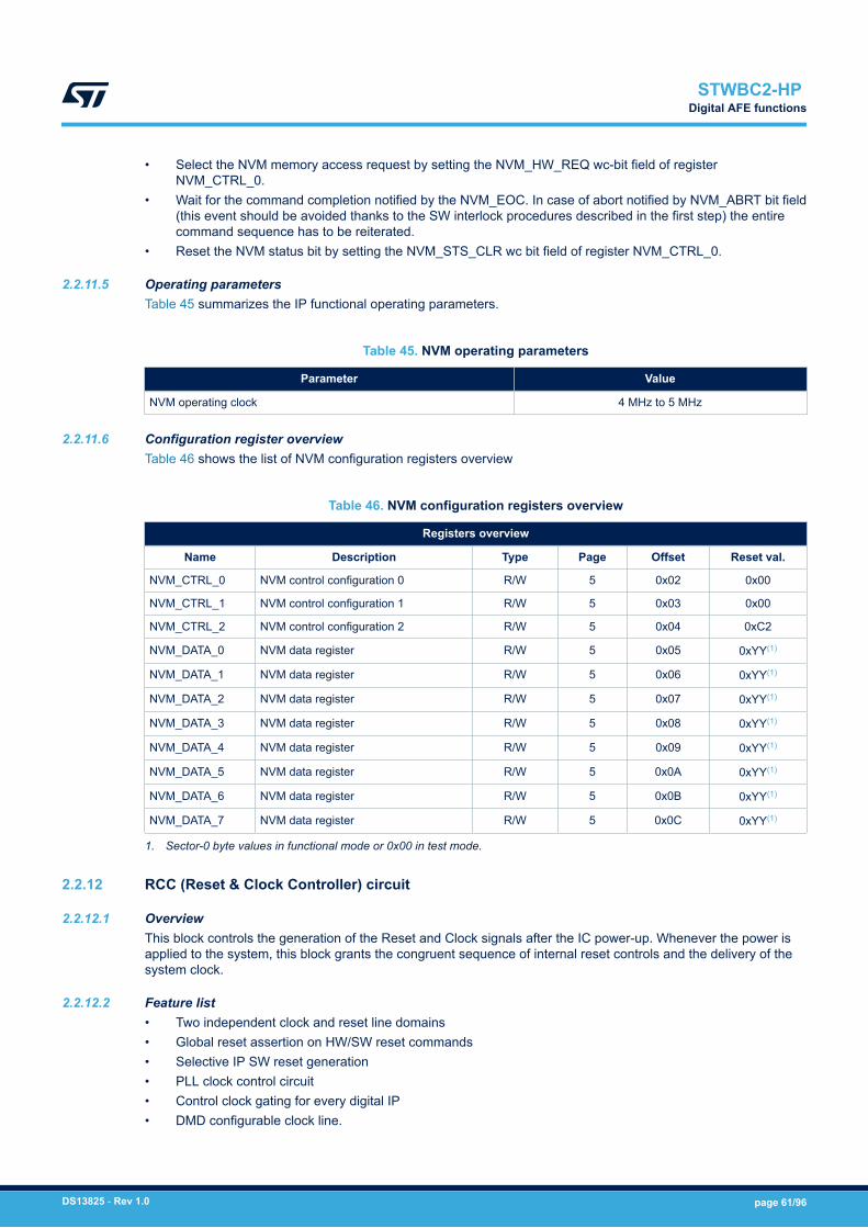
• Select the NVM memory access request by setting the NVM_HW_REQ wc-bit field of registerNVM_CTRL_0.
• Wait for the command completion notified by the NVM_EOC. In case of abort notified by NVM_ABRT bit field(this event should be avoided thanks to the SW interlock procedures described in the first step) the entirecommand sequence has to be reiterated.
• Reset the NVM status bit by setting the NVM_STS_CLR wc bit field of register NVM_CTRL_0.
2.2.11.5 Operating parametersTable 45 summarizes the IP functional operating parameters.
Table 45. NVM operating parameters
Parameter Value
NVM operating clock 4 MHz to 5 MHz
2.2.11.6 Configuration register overviewTable 46 shows the list of NVM configuration registers overview
Table 46. NVM configuration registers overview
Registers overview
Name Description Type Page Offset Reset val.
NVM_CTRL_0 NVM control configuration 0 R/W 5 0x02 0x00
NVM_CTRL_1 NVM control configuration 1 R/W 5 0x03 0x00
NVM_CTRL_2 NVM control configuration 2 R/W 5 0x04 0xC2
NVM_DATA_0 NVM data register R/W 5 0x05 0xYY(1)
NVM_DATA_1 NVM data register R/W 5 0x06 0xYY(1)
NVM_DATA_2 NVM data register R/W 5 0x07 0xYY(1)
NVM_DATA_3 NVM data register R/W 5 0x08 0xYY(1)
NVM_DATA_4 NVM data register R/W 5 0x09 0xYY(1)
NVM_DATA_5 NVM data register R/W 5 0x0A 0xYY(1)
NVM_DATA_6 NVM data register R/W 5 0x0B 0xYY(1)
NVM_DATA_7 NVM data register R/W 5 0x0C 0xYY(1)
1. Sector-0 byte values in functional mode or 0x00 in test mode.
2.2.12 RCC (Reset & Clock Controller) circuit
2.2.12.1 OverviewThis block controls the generation of the Reset and Clock signals after the IC power-up. Whenever the power isapplied to the system, this block grants the congruent sequence of internal reset controls and the delivery of thesystem clock.
2.2.12.2 Feature list• Two independent clock and reset line domains• Global reset assertion on HW/SW reset commands• Selective IP SW reset generation• PLL clock control circuit• Control clock gating for every digital IP• DMD configurable clock line.
STWBC2-HP Digital AFE functions
DS13825 - Rev 1.0 page 61/96

2.2.12.3 Functional descriptionFigure 59 shows the RCC block diagram.
Figure 59. RCC block diagram
2.2.12.4 Reset functionalityThe block uses the ASYNC_NRST_0 signal coming from the pad and the ASYNC_NRST_1 provided by a GPIOdriven from the FW application. These signals concur to generate the internal main reset signal in the two clockdomains.A selective reset may be generated by SW in order to reset a specific IP without impacting the functionalities ofother circuits.Figure 60 shows an outline view of the AFE reset circuit.
Figure 60. Reset circuit overview
Note: 1. SYNC_NRST_PLL_0 used for DOMAIN_NRST_OUT[13-152. PLL_CLK_GATED[0] used for DOMAIN_NRST_OUT[13-15]Note that the reset scheme is intended to show the circuit functionality and may be not aligned with the RTLimplementation.
STWBC2-HP Digital AFE functions
DS13825 - Rev 1.0 page 62/96

2.2.12.5 Clock functionalityThe AFE companion DIE has two asynchronous clock lines.• The main clock is originated by the MCU companion device after the initialization. The clock is
interconnected to a programmable divisor logic to select the AFE target operating frequency in a rangeof 8 – 16 MHz. The main clock is supplied to the PLL reference clock line in a range of 8 – 18 MHz.
• The high-speed clock is provided by a PLL phase locked circuit interconnected to a 17 phase DLL whichprovides 17 clocks up to 40 MHz
Note: After reset the CLK_OUT is equal to the CLK_IN.
Figure 61 shows the clock divisor circuit overview.
Figure 61. Clock divisor circuit overview
Figure 62 shows the clock enable circuit overview.
Figure 62. Clock enable circuit overview
Note: 1. SYNC_NRST_PLL_0 used for DOMAIN_CLK_OUT[13-15]2. PLL_CLK_GATED[0] used for DOMAIN_CLK_OUT[13-15]3. The clock enable controllability of PLL_CLK_GATED[15] is reserved4. PLL_CLK_GATE[16:0] clock lines are directly interconnected to the HR-PWM IP
2.2.12.5.1 DMD clockFigure 63 shows the clock circuit used to generate the demodulation comparator auto-zero offset functionality.
STWBC2-HP Digital AFE functions
DS13825 - Rev 1.0 page 63/96

Figure 63. DMD clock circuit overview
The clk_dmd is used in both current and voltage demodulator circuits to provide a fixed frequency closed to about100 kHz (+/-30%). The controllability of the above circuit is done through the DEMOD_CTRL register.The ENABLE bit controls the clock toggle functionality while the CLK_DIV represents the clock count.
The clk_out is divided by a fixed prescale value of 4-bits and is then counting the value configured in theCLK_DIV register field from 0x01 up to 0x7F.
The CLK_DMD equation is shown in the next equation.Fdmd = FafeClkdiv* Prescale + 1 *2 Where:• Prescale = 4• CLK_DIV is comprised between 0x01 up to 0x7F
2.2.12.5.2 PLL clock configurationThe PLL configuration parameters require first to disable the PLL by clearing the PLL_EN bit field of registerRCC_CLK_CONFIG_1 then configures both PLL_PRE_DIV and PLL_MULT bit fields belonging to registersRCC_CLK_CONFIG_1 and RCC_CLK_CONFIG_2, finally the PLL should be re-enabled by setting the PLL_ENbit.Any further register modification parameters require the iteration of the above procedures.The RCC provides clock and reset to 16 controllable domains (peripherals). The clock source of each domain isassigned to clk_out or pll_clk_gated[0]. Similarly, the async reset source for each domain is assigned to sync_nrstor sync_nrst_pll_0. The configuration is static (list of define).Table 47 shows the clock and reset signal vector assignment.
Table 47. RCC SW RST and Clock gating bit control
SW RST and Clock gating
bit Peripheral source Comment
0 RFU Reserved
1 Page 1 registers clk_out / sync_nrst BB-DCDC registers
2 Page 2 registers clk_out / sync_nrst HR-PWM registers
3 RFU Reserved
4 RFU Reserved
5 Page 5 registers(1) clk_out / sync_nrst Trimming registers, NVM and DFT registers
6 RFU Reserved
7 Reserved clk_out / sync_nrst Reserved
8 Common IPs clk_out / sync_nrst LEDs, ADC_MUXs, Prot, and ITC IPs
9 Phase demod. clk_out / sync_nrst Phase demodulator
10 RFU Reserved
11 RFU Reserved
12 RFU Reserved
STWBC2-HP Digital AFE functions
DS13825 - Rev 1.0 page 64/96

SW RST and Clock gating
13 BB-DCDC pll_clk_gated[0] /sync_nrst_pll_0 BB-DCDC IP
14 QF controller pll_clk_gated[0] /sync_nrst_pll_0 Qfactor IP
15 HR-PWM(2) sync_nrst_pll_0Controls only the reset. The clock of HR-PWMis directly provided by the pll_clk_gated[16:0] linesdisabling by PLL_ENABLE signal.
1. The trimming and DFT registers are reset with the main reset signal line.2. The clock enable controllability PLL_CLK_GATED[15] line is reserved.
2.2.12.6 Operating parametersTable 48 summarizes the IP functional operating parameters:
Table 48. RCC operating parameters
Parameter Value Comment
AFE input clock (CLK_IN) 16 MHz Basic clock low speed
PLL reference output clock 16 MHz Synch. with CLK_IN
CLK_OUT output clocks 16 MHz Synch. with CLK_IN
PLL_CLK input clock 40 MHz Clock high speed
PLL_CLK_GATED output clocks 40 MHZ Synch. with PLL_CLK
CLK_DMD output clock 100 kHz Synch. with CLK_IN
2.2.12.7 Configuration register overviewTable 49 shows the list of RCC configuration registers overview:
Table 49. RCC configuration registers overview
Registers overview
Name Description Type Page Offset Reset val.
RCC_CLOCK_EN_0 Clock enabling of digital cells 0 R/W 0 0x38 0xFF
RCC_CLOCK_EN_1 Clock enabling of digital cells 1 R/W 0 0x39 0xFF
RCC_RESET_N_0 Reset of digital cells 0 R/W 0 0x3A 0xFF
RCC_RESET_N_1 Reset of digital cells 1 R/W 0 0x3B 0x1F
RCC_CLK_CONFIG_0 Clock configuration 0 R/W 0 0x3C 0x00
RCC_CLK_CONFIG_1 Clock configuration 1 R/W 0 0x3D 0x00
RCC_CLK_CONFIG_2 Clock configuration 2 R/W 0 0x3E 0x00
RCC_STATUS Reset and clock status R 0 0x3F 0x0Y(1)
1. Refer to register definition.
2.2.13 SPI slave interface
2.2.13.1 OverviewThis block is the AFE communication interface with the MCU companion DIE; the SPI slave interface decodesSPI serial signals and generates a corresponding parallel peripheral bus transaction.
Figure 64 shows the SPI block diagram overview.
STWBC2-HP Digital AFE functions
DS13825 - Rev 1.0 page 65/96

Figure 64. SPI block diagram overview
2.2.13.2 Feature list• Slave 16bits serial interface to master parallel peripheral bus• Complete asynchronous link between the SPI and PB bus• Clock ratio of spi_clk vs afe_clk is 2• Supports multi-byte read and write with fixed, auto-increment or explicit address• Supports read-modify-write atomic sequence• Serial data order from MSB to LSB• Disable synchronizer stages in ATE test mode
2.2.13.3 Functional descriptionThe cell has 2 separate clock domains:
Figure 65. SPI clock domain overview
• The spi_clk domain contains the serial engine. It is reset with resetn and partially also with spi_csn.• The clk domain generates parallel peripheral bus access corresponding to the SPI transaction.
The spi_clk domain serializer/deserializer is reset with spi_csn at 1. Hence, the machine restarts from scratch ateach new SPI access.The serial machine is clocked on neg edge of spi_clk. During the SPI transaction, the machine decodes theaccess direction, the access address and the eventual write data.
STWBC2-HP Digital AFE functions
DS13825 - Rev 1.0 page 66/96

The addr vector is asynchronously provided to the peripheral bus based on the spi_clk. The peripheral bus readoperation being completely combinational, there is no synchronization between clk and spi_clk domain.The clk domain receives access request from the spi_clk domain through read and write toggling flags. Theseflags are synchronized on clk domain with dual edge. Since a flag is seen toggled, the clk domain generates thecorresponding re or we pulse. The addr and wdata vectors are guaranteed to be static before and during the re orwe pulse generated on clk domain.Here below is shown the SPI basic timing diagram.
Figure 66. MCU-SPI interface timing diagram overview
The next section details all the supported transaction operations.
2.2.13.3.1 Single byte write access:The first byte transmitted by the master after NSS goes low corresponds to the access address. The MSB of thisbyte is 0, meaning that it is a write access. During the transmission of the first byte, the slave transmits 8bits dataat 0.The second byte sent by the master is the 8bits data to be written at the requested address. While the databyte to be written is sent by the master, the slave transmits the value at address+1. This offers the possibility tocombine a write and read on adjacent address.The write process stops when NSS comes high.
Figure 67. Single byte write access
2.2.13.3.2 Single byte read access:The first byte transmitted by the master after NSS goes low corresponds to the access address. The MSB of thisbyte is 1 meaning that it is a read access. During the transmission of the first byte, the slave transmits 8bits dataat 0.The second byte sent by the master is not used and must be 0. During the master transmission of second byte,the slave transmits the value at address.The read process stops when NSS comes high.
STWBC2-HP Digital AFE functions
DS13825 - Rev 1.0 page 67/96

Figure 68. Single byte read access
2.2.13.3.3 Multiple byte write access with address auto-increment:The auto-increment is activated with a specific signal of the I/F.The first byte transmitted by the master after NSS goes low corresponds to the initial access address. The MSB ofthis byte is 0, meaning that it is a write access. During the transmission of the first byte, the slave transmits 8bitsdata at 0.The second byte sent by the master is the 8bits data to be written at the requested address. While the databyte to be written is sent by the master, the slave transmits the value at address+1. This offers the possibility tocombine a write and read on adjacent address.For each following byte, the address of the access is automatically incremented up to 0x7F. When 0x7F isreached, the address is no more incremented.The write process stops when NSS comes high.
Figure 69. Multiple byte write with address auto-increment
2.2.13.3.4 Multiple byte write access at fixed address:The auto-increment is deactivated with a specific signal of the I/F.The first byte transmitted by the master after NSS goes low corresponds to the initial access address. The MSB ofthis byte is 0, meaning that it is a write access. During the transmission of the first byte, the slave transmits 8bitsdata at 0.The second byte sent by the master is the 8bits data to be written at the requested address. While the databyte to be written is sent by the master, the slave transmits the value at address+1. This offers the possibility tocombine a write and read on adjacent address.For each following byte, the address of the access is the same. This mode of operation fits perfectly with a FIFOfill operation.The write process stops when NSS comes high.
Figure 70. Multiple byte write with fixed address
2.2.13.3.5 Multiple byte read access with explicit addresses:The first byte transmitted by the master after NSS goes low corresponds to the first access address. The MSB ofthis byte is 1, meaning that it is a read access. During the transmission of the first byte, the slave transmits 8bitsdata at 0.Each following byte transmitted by the master corresponds to a new address on which the read has to be done.These bytes must have their MSB bit at 1. During the transmission of the new address, the slave responds to thedata read at the previous address request.The read process stops when NSS comes high.
STWBC2-HP Digital AFE functions
DS13825 - Rev 1.0 page 68/96

Figure 71. Multiple byte read access with explicit address
2.2.13.3.6 Multiple byte read access with address auto-increment:The auto-increment is activated with a specific signal of the I/F.The first byte transmitted by the master after NSS goes low corresponds to the first access address. The MSB ofthis byte is 1, meaning that it is a read access. During the transmission of the first byte, the slave transmits 8bitsdata at 0.Each following byte must be 0 to engage the auto-increment of the address. The address of the access isautomatically incremented up to 0x7F. When 0x7F is reached, the address is no more incremented.The read process stops when NSS comes high.
Figure 72. Multiple byte read access with address auto-increment
2.2.13.3.7 Multiple byte read access at fixed address:The auto-increment is deactivated with a specific signal of the I/F.The first byte transmitted by the master after NSS goes low corresponds to the first access address. The MSB ofthis byte is 1, meaning that it is a read access. During the transmission of the first byte, the slave transmits 8bitsdata at 0.Each following byte must be 0 to engage the fixed address access. For each byte, the slave transmits the dataread at the same address. This mode is useful to read a FIFO content at a fixed address.The read process stops when NSS comes high.
Figure 73. Multiple byte read access at fixed address
2.2.13.3.8 Read-Modify-Write access:The Read-Modify-Write (RMW) access allows modifying one bit or two contiguous bits at a given position in aregister.The first byte transmitted by the master after NSS goes low corresponds to the access address. The MSB of thisbyte is 1, meaning that it is a read access. During the transmission of the first byte, the slave transmits 8bits dataat 0.The second byte transmitted must have bit 7 = 0 and bit 6 = 1. This informs the SPI slave that access is an RMW.Bit 5, called n, informs of the number of bits to modify. If bit 5 = 0, only 1 bit is modified. If bit 5 = 1, 2 bits aremodified.Bit 4 & 3, called bits[1:0], gives the bit value to set in the register. If the RMW is only 1bit, the bits[0] bit is used.Bit 2, 1 & 0, called pos[2:0], gives the position in the register byte to apply the bit modification.
STWBC2-HP Digital AFE functions
DS13825 - Rev 1.0 page 69/96

Figure 74. Read Modify Write access
Example 1:• Register is 8’b00110100• RMW operation is done on 1 bit, pos[2:0] = 1 and bits[0] = 1.• Then register becomes 8’b00110110
Example 2:• Register is 8’b00110100• RMW operation is done on 2 bit, pos[2:0] = 2 and bits[1:0] = 2’b10.• Then register becomes 8’b00111000
2.2.13.4 Operating parametersTable 50 summarizes the IP functional operating parameters.
Table 50. SPI operating parameters
Parameter Value
Operating frequency 16 MHz
SPI frequency 16 MHz
Note: The minimum clock ratio of SPI_CLK vs AFE_CLK is 2.
2.2.14 Register sub-system
2.2.14.1 OverviewThis block is a multifunction IP which includes the page register bank selection and the data register arrayselected by the page register contents.Figure 75 shows the page register bank selection block diagram.
STWBC2-HP Digital AFE functions
DS13825 - Rev 1.0 page 70/96

Figure 75. Register subsystem diagram overview
2.2.14.2 Feature list• Provides page selection register• Performs read data mux• Data register array (8bits registers with R/W, R only or self-clearing bit-fields)• Register banks organization:
– Bank-0: Miscellaneous registers of common peripherals– Bank-1: BB-DCDC configuration registers– Bank-2: HR-PWM configuration registers– Bank-5: Manufacturing trimming parameters, NVM and DFT registers– Bank-7: Reserved for FPGA emulator environment
2.2.14.3 Functional description
2.2.14.3.1 Page register:Here below is shown the internal block diagram of the page register selection.
STWBC2-HP Digital AFE functions
DS13825 - Rev 1.0 page 71/96

Figure 76. Page Register sub-block diagram overview
The register sub-system is arranged around a page select cell and a single register located at address 0. Theaddress 0 register is always accessed since the PB bus address is 0. This register has the following layout:
Offset: 0x00Default Value: 0x00PAGE_REGISTER Control Interface
7 6 5 4 3 2 1 0
auto_inc RFU page_sel
R/W R R/W
R/W R R/W
• auto_inc bit: this bit is provided to the SPI slave interface to control the auto increment of access address.• page_sel[2:0]: this vector is provided to the page select cell in order to select a page of registers.
2.2.14.4 Operating parametersTable 51 summarizes the IP functional operating parameters:
Table 51. Register subsystem operating parameters
Parameter Value
Bus data width 8 bits
Bus address width 7 bits
2.2.14.5 Configuration register overviewTable 52 shows the list of Register subsystem configuration registers overview:
STWBC2-HP Digital AFE functions
DS13825 - Rev 1.0 page 72/96

Table 52. Reg. subsystem configuration registers overview
Registers overview
Name Description Type Page Offset Reset val.
PAGE_SELECTION Register at address 0 as described in celldescription section R/W 0 0x00 0x00
Note: For data register description please contact our sales representative.
STWBC2-HP Digital AFE functions
DS13825 - Rev 1.0 page 73/96

3 Electrical data
3.1 Absolute Maximum RatingsStresses above the absolute maximum ratings listed in Table 53 may cause permanent damage to the device.Exposure to maximum rating conditions for extended periods may affect device reliability.
Table 53. Absolute maximum ratings
Symbol Parameter Test condition Min. Max. Unit
VIN Power supply voltage (VIN) - -0.3 27 V
VDD_DRIVERGate driver supply voltage(VDD_DR) -0.3 15 V
VLSn_GDLow-side gate driver voltage(LS1_GD, LS2_GD, LS3_GD) -0.3 VDR + 0.3 V
VHBn_SWHB Switching node voltage(HB1_SW, HB2_SW, HB3_SW) -2 50 V
VBRG_VSNS BRG_VSNS, DCDC_SNS -0.3 50 V
VHBn_BTHB Bootstrap voltage (HB1_BT,HB2_BT, HB3_BT)
Max(VHBn_SW - 0.3or -0.3)
Min((VHBn_SW + VDR +0.3) or 60) V
VHSn_GDHB High-side gate driver voltage(HS1_GD, HS2_GD, HS3_GD) VHBn_SW -0.3 VHBn_BT V
VDD Input voltage for Analog die (VDD) -0.3 5.5 V
VBUCK_SWBuck switching node voltage(BUCK_SW) -1 27 V
VBUCK_BOOTBuck bootstrap voltage(BUCK_BOOT) -0.3 32.0 V
VIN_SNSVin sense voltage (VIN_ISNS_P,VIN_ISNS_M, VIN_SNS) -0.3 Vin V
VLDO_3V3Input voltage for MCU die(LDO_3V3, VREF_A, MCU_3V3) -0.3 4 V
VIO_TT
MCU logic input voltage (I/O TTstructure pins – see
Internal signal connection
Table 38)
-0.3 4 V
VIO_FT
MCU logic input voltage (I/O FTstructure pins – see
Internal signal connection
Table 38)
-0.3 VLDO_3V3 + 4 V
VIO_DRVGeneral purpose driver I/Os(GP_DRV<0:3>) -0.3 4 V
VNRST NRST I/O -0.3 4 V
VLDO_1V8Supply voltage for digital circuitry(LDO_1V8) -0.3 2 V
STWBC2-HP Electrical data
DS13825 - Rev 1.0 page 74/96

Symbol Parameter Test condition Min. Max. Unit
VIO_AN
Analog pin voltage (BUCK_FB,BRG_ISNSP, BRG_ISNSM,BRG_SNSB, BRG_IDEM,BRG_FT_R, BRG_FT_S,RNG_FT_R, RNG_FT_S,RNG_SNS, USB_DP, USB_DM,QF_DRV,LED1,LED2)
-0.3 VDD V
TSTG Storage temperature -55 150 °C
3.2 Recommended Operating Conditions
Table 54. Recommended operating conditions
Symbol Parameter Testcondition Min. Typ. Max. Unit
VIN Power supply voltage - 4.1 24 V
Power supply voltage slope VIN=22V 100 V/μs
VDD_DRIVERVoltage doubler output and gate driversupply voltage 5 7.5 10 V
VBUCK_SW Buck switching node voltage (BUCK_SW) 24 V
VBUCK_BOOT Buck bootstrap voltage (BUCK_BOOT) 29 V
VHBn_BTHB bootstrap voltage (HB1_BT, HB2_BT,HB3_BT) 50 V
VHBn_SWHB switching node voltage (HB1_SW,HB2_SW, HB3_SW) 40 V
VDDBuck regulator output and input voltage forAnalog die 3.4 5.2 V
LBUCK Buck regulator inductance 10 22 μH
CBUCK Buck regulator capacitance 10 μF
ESRBUCK Buck regulator capacitance ESR 0.1 ◻
VLDO_3V3Linear regulator output and input voltagefor MCU die 3.0 3.3 3.6 V
CLDO_3V3 Linear regulator output capacitance 4.7 22 μF
VLDO_1V8Linear regulator output and supply voltagefor digital circuitry 1.8 1.95 V
C LDO_1V8 Linear regulator output capacitance -20% 4.7 +20% μF
VHS HB floating supply voltage(2) VDD_DRIVER(1) 10 V
Tj Operating junction temperature -40 125 °C
1. VHS = VBT_HS - VHB_SW
3.3 ESD Protections
Table 55. ESD protection ratings
Symbol Parameter Test condition Value Unit
HBM Conforming to ANSI/ESDA/JEDEC 2 kV
STWBC2-HP Recommended Operating Conditions
DS13825 - Rev 1.0 page 75/96

Symbol Parameter Test condition Value UnitHuman body model JS-001-2014
CDM Charged device modelConforming to ANSI/ESDA/JEDEC
JS-001-2014250 kV
3.4 Thermal data
Table 56. Thermal data
Symbol Parameter Value Unit
Rth(JA) Thermal resistance junction to ambient 45 °C/W
3.5 Electrical characteristicsConditions: VIN=12 V, VDD_DRIVER=7.5 V, VDD=5 V, VLDO_3V3=3.3 V, VLDO_1V8=1.8 V, TJ from -40°C to125°C, CLSn_GD=CHSn_GD=1 nF, CBRIDGE_VREF=10 nF, LBUCK=10 μH, CLDO_1V8=1 μF, CLDO_3V3=4.7 μF,CBUCK=10 μF (ceramic capacitor), CEXT=6.8 nF, REXT=100 kohm (CEXT with REXT is AC coupling networkon RING_NODE_SNS), CQFDRV_VRING=2.2 nF (coupling cap for Q-factor measurement), LBUCKBOOST=3.6 μH,CD+=CD-=100 pF; unless otherwise noted.Typical values are tested at TJ = 25°C, minimum and maximum values are guaranteed by thermalcharacterization in the temperature range of -40 to 125°C, unless otherwise specified.
Table 57. Electrical charachteristics
Symbol Parameter Test condition Min. Typ. Max. Unit
POWER SUPPLY
IIN_STBYPower supply currentconsumption in quiescentstate
VIN=22 V;
VDD_DRIVER=7.5 V,
VDD=5 V externally supplied
0.5 mA
Fault condition, NRST=0
VIN=22 V;
VDD_DRIVER=7.5 V,
VDD=3.6 V externally supplied
0.5 mA
VINon VIN UVLO turn-on threshold VIN rising from 0 V 2.5 3.5 V
IDD_DRIVERVDD_DRIVER currentconsumption
VDD_DRIVER=7.5 V externallysupplied, no commutation. 0.2 mA
IVDD VDD current consumption
VDD=5 V
fSW=100 kHz (system frequency)10 15 mA
QF on
VIN=22 V;
VDD_DRIVER=7.5 V,
VDD=5 V
5 mA
Standby (NRST=0) VDD=3.6 V
Tj = 25°C0.5 mA
Standby (NRST=0) VDD=3.6 V
Tj = 125°C1 mA
VON,VDD3V6
VDD UVLO turn-onthreshold at startup (notrimming)
VDD turn-on threshold 3.25 3.35 3.45 V
STWBC2-HP Thermal data
DS13825 - Rev 1.0 page 76/96

Symbol Parameter Test condition Min. Typ. Max. Unit
VOFF,VDD3V6
VDD UVLO turn-offthreshold
(with 3.6 V selection)
VDD turn-off threshold 3.25 3.35 3.45 V
VOFF,VDD5V
VDD UVLO turn-offthreshold (with 5 Vselection)
VDD turn-off threshold 4.55 4.65 4.75 V
TDELAY_VDDComparator propagationdelay dV/dt=100 mV/ms 1 μs
TFILTER_VDD Comparator output filter -25% 1 +25% μs
NRST PIN(1)
VIL(NRST)NRST input low levelvoltage 0.3 x VLDO_3V3 V
VIH(NRST)NRST input high levelvoltage 0.7 x VLDO_3V3 V
Vhys(NRST)NRST Schmitt triggervoltage hysteresis
0.6 x
VLDO_3V3mV
RPUWeak pull-up equivalentresistor(2)
STM32G071 parameter,
VSS=VLDO_3V375 kΩ
BUCK SWITCHING REGULATOR
VIN
VIN operative range forVDD=5 V 5.5 24 V
VIN operative range forVDD=3.6 V 4.1 24 V
VBUCK_FB Average output voltageVDD=5 V selection, VIN ≥ 6V 4.75 5.0 5.25 V
VDD=3.6 V selection, VIN ≥ 4.5V 3.42 3.6 3.78 V
ILOAD Output load current 450 mA
DVBUCK_FB_DO VDD Dropout VoltageILOAD=[0÷450] mA DC;
VDD=3.6 V/5 V500 mV
IVALLEYLIMIT_BUCK Valley Current Limit L=10 μH 450 600 750 mA
IPEAKLIMIT_BUCK Peak Current Limit In Low-Dropout operations only 700 900 1100 mA
fSW_BUCK Switching frequencyCCM when not in LDO,
L=10 μH1 MHz
RDSON_HSBuck switching node pull-upresistance ILOAD=100 mA, TJ = 25°C 300 430 685 mΩ
RDSON_LSBuck switching node pull-down resistance ILOAD=100mA, TJ = 25°C 240 340 540 mΩ
LINEAR REGULATORS
VLDO_3V3LDO_3V3 regulationvoltage
ILDO_3V3=[0÷150] mA;
VDD=[3.4÷5.25] V3.1 3.3 3.5 V
ILDO_3V3LDO_3V3 DC currentcapability 150 mA
◻VLDO_3V3_DO LDO_3V3 dropout voltageILDO_3V3=150 mA DC;
VDD=3.1 V350 mV
ILIMIT_LDO3V3LDO_3V3 output currentlimit Trimmed parameter 270 380 520 mA
CLDO_3V3LDO_3V3 outputcapacitance allowed range Ceramic capacitor 4.7 22 μF
VLDO_1V8LDO_1V8 regulationvoltage
ILDO_1V8=[0÷50] mA;
VDD=[3.4÷5.25] 1.7 1.8 1.9 V
ILDO_1V8LDO_1V8 DC currentcapability 50 mA
STWBC2-HP Electrical characteristics
DS13825 - Rev 1.0 page 77/96

Symbol Parameter Test condition Min. Typ. Max. Unit
ILIMIT_LDO1V8LDO_1V8 output currentlimit Trimmed parameter 80 160 mA
CLDO_1V8LDO_1V8 outputcapacitance allowed range Ceramic capacitor -20% 4.7 +20% μF
VON,V3V3 VLDO_3V3 rising voltage 2.85 2.95 3.05 V
VOFF,V3V3 VLDO_3V3 falling voltage 2.7 2.8 2.9 V
TDELAY_V3V3Comparator propagationdelay dV/dt=100 mV/ms 1 μs
TFILTER_V3V3 Comparator output filter -25% 0.85 +25% μs
VON,V1V8 VLDO_1V8 rising voltage 1.67 1.7 1.73 V
VOFF,V1V8 VLDO_1V8 falling voltage 1.64 1.67 1.7 V
TDELAY_V1V8 Comparator propagationdelay dV/dt=100 mV/μs 1 μs
TFILTER_V1V8 Comparator output filter -25% 0.85 +25% μs
VOLTAGE DOUBLER CONTROL
fSW_VOLTDOUBLE_RNGSwitching frequency range(clock source from AFE/PLL)
0.01 1 MHz
RUP_VOLTDOUBLEInternal
PMOS ON-resistance10.5 Ω
RDOWN_VOLTDOUBLEInternal
NMOS ON-resistance3.5 Ω
BUCK BOOST DC DC
VINVIN
operating range4.1 24 V
fSW_BBOperating
frequency1 MHz
VBRIDGE Output voltage Selectable via FW
1 V
14 V
18 V
24 V
30 V
40 V
GATE DRIVERS
GD1RUPGate driver 1 high-side onresistance TJ = 25°C 5 Ω
GD1RDWNGate driver 2 low-side onresistance TJ = 25°C 2.5 Ω
GD2RUPGate driver 2 high-side onresistance TJ = 25°C 5 Ω
GD2RDWNGate driver 2 low-side onresistance TJ = 25°C 2.5 Ω
GD3RUPGate driver 3 high-side onresistance TJ = 25°C 5 Ω
GD3RDWNGate driver 3 low-side onresistance 2.5 Ω
LED DRIVER (can be bypassed to 5 V-GPIO with pad operating voltage VDD)
ILEDDRV Sink current values
2.5 mA
5 mA
7.5 mA
10 mA
ILEDDIM Dimming current step 2.5 mA
STWBC2-HP Electrical characteristics
DS13825 - Rev 1.0 page 78/96

Symbol Parameter Test condition Min. Typ. Max. Unit
ILED_FREQ Pattern frequency 10 kHz
VLED_ILGPIO operations(2): lowinput voltage level 0.8 V
VLED_IHGPIO operations(2): highinput voltage level 2 V
VLED_OLGPIO operations(2): lowoutput voltage level
ILOAD=6 mA (sourced) 0.4 V
VLED_OHGPIO operations(2): highoutput voltage level
ILOAD=-6 mA (sunk)VLDO_3V3-
0.4V
fLED_GPIOGPIO operations(2):operating frequency C=50 pF 2 MHz
Q-FACTOR DRIVER
VRING_NODE_RNG Oscillation amplitude Steady-state with ZCD lock 0.020 1 2 Vpp
EIQF_SINKSink current capability erroron all steps
VDD=5 V
VQF_DRV≤VDD-0.5 V
SHORT=0, IQF_SOURCE=0
10 %
EIQF_SOURCESource current capabilityerror on all steps
VDD=5 V
VQF_DRV≥0.5 V
SHORT=0, IQF_SINK=0
10 %
EΔI Sink/Source mismatch erroron all steps
VDD=5 V
VQF_DRV=VDD/2
SHORT=0
7 %
ISELCurrent programmable stepcount (excluded off state) 16
IQF_STEP Current regulation step 250 μA
RINGING NODE VOLTAGE SENSE & DEMODULATION
IRING_NODE
RING_NODE_SNS inputcurrent
during power transfer
V-I conversion is made by meansof 100 kΩ external resistor. ±0.01 ±1 mA
RING_NODE_SNS inputcurrent
during Q-factormeasurement
V-I conversion is made by meansof 100 kΩ external resistor. ±0.1 ±10 μA
fRING_NODECurrent & Voltagefrequency range 100 300 kHz
RGAIN_NODE_SNSTrans-resistance gainvalues of the internal I-Vconverter
IRING_NODE=±[0.8÷1] mA 2.2 kW
IRING_NODE=±[0.6÷0.8] mA 3.0 kW
IRING_NODE=±[0.44÷0.6] mA 4.0 kW
IRING_NODE=±[0.32÷0.44] mA 5.4 kW
IRING_NODE=±[0.24÷0.32] mA 7.4 kW
IRING_NODE=±[0.18÷0.24] mA 9.9 kW
IRING_NODE=±[0.135÷0.18] mA 13.2 kW
IRING_NODE=±[0.060÷0.135] mA 17.7 kW
IRING_NODE=±[0.025÷0.060] mA 39.4 kW
IRING_NODE=±[0.001÷0.025] mA 94.8 kW
IRING_NODE=±[4÷1] μA(3) 224.8 kW
IRING_NODE=±[1.6÷4] μA(3) 566.2 kW
IRING_NODE=±[0.1÷1.6] μA(3) 1442 kW
fLPF_NODESNSDEMODLow pass filter frequencyvalues
-10% 4 +10% kHz
STWBC2-HP Electrical characteristics
DS13825 - Rev 1.0 page 79/96

Symbol Parameter Test condition Min. Typ. Max. Unit
fLPF_NODESNSDEMODLow pass filter frequencyvalues
-10% 8 +10% kHz
-10% 12 +10% kHz
-10% 16 +10% kHz
fHPF_NODESNSDEMODHigh pass filter
cut-off frequency values
-10% 300 +10% Hz
-10% 450 +10% Hz
-10% 600 +10% Hz
-10% 750 +10% Hz
BRIDGE CURRENT SENSE & DEMODULATION
IBRIDGE_ZCDZero cross detection offsetvoltage
Between BRIDGE_ISNS_P andBRIDGE_ISNS_N -10 0 +10 mV
VBDG_CURRSNS_CMSensing resistor commonmode voltage 0 V
VBDG_CURRSNS_RNGSensing resistor differentialvoltage range
Between BRIDGE_ISNS_P andBRIDGE_ISNS_N ±0.02 ±200 mV
GBDG_CURRSNS
Bridge Current Sense Gain
Four selectable values: 4, 8,16, 32.
4 32 V/V
ZIN_BDGCURRSNS Differential input impedance 5 kΩ
IIN_BDGCURRSNS Input Current 5 mA
fLPF_BDGCURRDEMODLow pass filter
cut-off frequency values
-10% 4 +10% kHz
-10% 8 +10% kHz
-10% 12 +10% kHz
-10% 16 +10% kHz
fHPF_NODESNSDEMODHigh pass filter
cut-off frequency values
-10% 300 +10% Hz
-10% 450 +10% Hz
-10% 600 +10% Hz
-10% 750 +10% Hz
VIN CURRENT SENSE
VIN_CURR_SNS_CMCommon mode voltage onsense resistor 4 24 V
VIN_CURR_SNS_RNGDifferential input voltagerange (across senseresistor)
±16 ±200 mV
IIN_CURR_SNS_CMCommon mode inputcurrent (through sensenodes)
5 mA
ZIN_CURR_SNS_CM Input differential impedance 50 Ω
EXTERNAL GATE DRIVERS (GPIOs with pad operating voltage VLDO_3V3)
VGP_IL Input low level voltage 0.8 V
VGP_IH Input high level voltage 2 V
VGP_OL Output low level voltage ILOAD=6 mA (sourced) 0.4 V
VGP_OH Output high level voltage ILOAD=- 6 mA (sunk)VLDO_3V3-
0.4V
fGP Output signal frequency C=50 pF, VLDO_3V3 25 MHz
COUT Pin capacitance 5 pF
PLL
fPLL Output frequency 40 68 MHz
HIGH RESOLUTION PWM GENERATOR
PWM_RES PWM resolution PLL frequency=40 MHz 1.47 ns
USB INTERFACE
STWBC2-HP Electrical characteristics
DS13825 - Rev 1.0 page 80/96

Symbol Parameter Test condition Min. Typ. Max. Unit
VGEN_DP(DM)DP & DM
generator
0.6 V voltage mode,
ILOAD: 0 ÷ 1 mA0.5 0.6 0.7 V
3.3 V voltage mode,
ILOAD: 0 ÷ 1 mA3.0 3.3 3.6 V
2.8 V voltage mode,
ILOAD: 0 ÷ 1 mA2.6 2.8 3.0 V
Current Mode Boundaries(4) 25 175 μA
IVGEN_DP(DM)VGEN_DP(DM) voltagegenerator current capability 0.5 1 mA
IDM_SINK/IDP_SINKSink current from USB_DMor USB_DP pad See STM32G071 62 100 144 μ
A
VISINK_DP(DM)IDP(DM)_SINK currentgenerator operative voltage 0.1 V
RLD_DP(DM)USB_DP & USB_DM pull-down resistance Pull-down mode - 20 k◻ load 16 20 24 kΩ
TSETT_VGEN_DM(DP) Configuration settling time 50 μs
1. See STM32G071 datasheet for details about NRST MCU pin.2. LED driver bypassed, direct pin driving (5 V GPIO).3. To be used during Q-factor measurement only.4. For source current less than IDP_SINK min. (25 μA), the voltage on USB_DP pin is required to be no higher than VDAT_SINK
max. (150 mV). For USB_DP voltage lower than VLGC max. (2 V) the current sunk from USB_DP pin shall to not higher thanIDP_SINK max. (175 μA). Same requirements apply to USB_DM pin.
STWBC2-HP Electrical characteristics
DS13825 - Rev 1.0 page 81/96

4 STWBC2-HP pinout and pin description
4.1 PinoutThis section shows the pinout used by the STWBC2-HP.
Figure 77. STWBC2-HP pin connection (top view)
Table 58. Pinout description
Pin Number Pin Name Pin Type Description
EP GND Power AFE substrate GND
1 IRQ Digital I/O Interrupt pin or GPIO ( PC15-OSC32-OUT )
2 LDO_3V3 Power LDO 3.3 V output (VBAT)
3 VREF_A Analog Out Analog reference voltage (VREF+)
4 MCU_3V3 Power MCU 3.3V supply input (VDD/VDDA)
5 LDO_1V8 Power LDO 1.8 V output
6 VDD Power AFE 5 V supply input
7 MCU_VSS Power MCU GND (VSS/VSSA)
STWBC2-HP STWBC2-HP pinout and pin description
DS13825 - Rev 1.0 page 82/96

Pin Number Pin Name Pin Type Description
8 MCU_VSS1 Power MCU GND (VDD_VREFM)
9 BUCK_FB Analog In DCDC 5 V output (feedback)
10 XTAL_IN Digital In PF0- XTAL in pin (OSC driver in)
11 XTAL_OUT Digital Out PF1 -XTAL out pin
12 NRST Digital I/O PF2 - nRST
13 PGND Power AFE analog Ground
14 BUCK_SW Analog Out Embedded DCDC Buck switching node
15 BUCK_BT Power Embedded DCDC Buck bootrstrap
16 VIN Power Input voltage
17 VIN_ISNS_P Analog In VIN current sensor Plus
18 VIN_ISNS_M Analog In VIN current sensor Minus
19 TEMPSNS Analog In ADC input for temperature sense
20 SPI_CLK Digital I/O SPI CLK
21 UART_TX Digital I/O USART Tx
22 UART_RX Digital I/O USART Rx
23 SPI_MISO Digital I/O SPI MISO
24 SPI_MOSI Digital I/O SPI MOSI
25 SPI_NSS Digital I/O SPI NSS
26 VDOUB_SW Analog Out Charge pump
27 VDD_DR Power Gate driver supply voltage
28 HS1_BT Power High-side gate driver bootstrap cap
29 HS1_GD Analog Out High-side gate driver output
30 HS1_SW Analog In Half-bridge switching node and voltage sense for DCDCbuck stage
31 LS1_GD Analog Out Low-side gate driver output
32 LS2_GD Analog Out Low-side gate driver output
33 DCDC_SNS Analog In Voltage sense for DCDC boost stage
34 HS2_SW Analog In Half-bridge switching node
35 HS2_GD Analog Out High-side gate driver output
36 HS2_BT Power High-side gate driver bootstrap cap
37 HS3_BT Power High-side gate driver bootstrap cap
38 HS3_GD Analog Out High-side gate driver output
39 HS3_SW Analog In Half-bridge switching node
40 LS3_GD Analog Out Low-side gate driver output
41 GND_DR Power Gate driver ground
42 GPIO_DR0 Analog Out Logic level pin to drive ext. gate driver
43 GPIO_DR1 Analog Out Logic level pin to drive ext. gate driver
44 GPIO_DR2 Analog Out Logic level pin to drive ext. gate driver
45 GPIO_DR3 Analog Out Logic level pin to drive ext. gate driver and DC voltagesensing function
46 LED1 Analog Out LED 1
47 LED2 Analog Out LED 2
STWBC2-HP Pinout
DS13825 - Rev 1.0 page 83/96

Pin Number Pin Name Pin Type Description
48 SWDIO Digital I/O Debugger IO
49 SWCLK Digital I/O Debugger CLK
50 BRG_VSNS Analog In Bridge voltage sense
51 DCDC_FB Analog In DCDC feedback pin
52 BRG_ISNS_M Analog In Bridge current sense Minus
53 BRG_ISNS_P Analog In Bridge current sense Plus
54 BRG_VREF Analog In/Out External filtering for internal voltage reference
55 BRG_IDEM Analog In Bridge current demodulation input
56 BRG_FT_S Analog Out Bridge LP filter send
57 BRG_FT_R Analog In Bridge LP filter return
58 CC1 Analog I/O USB power delivery CC1 pin
59 USB_DP Analog I/O USB D+ pin
60 USB_DM Analog I/O USB D- pin
61 CC2 Analog I/O USB power delivery CC2 pin
62 I2C_SDA Digital I/O I2C SDA
63 I2C_SCL Digital I/O I2C SCL
64 RNG_FT_S Analog Out Ringing node LP filter Send
65 RNG_FT_R Analog In Ringing node LP filter Return
66 QF_DRV Analog Out Q factor driver output
67 RNG_SNS Analog In Ringing node sense / PC14-OSC32-IN
68 AGND Power AFE analog Ground
4.2 Internal signal connection
Table 59. STWBC2-HP PAD Mapping
STWBC2-HPpin AFE pad MCU Pad MCU Function Type I/O
structure
EP SUB<1:2> - - A -
1 - PC15-OSC32-OUT PC15 I/O FT
2 LDO_3V3 <1:2> VBAT VBAT I/O -
3 - VREF+ VREF_OUT I/O -
4 - VDD<1:3> VDD S -
5 LDO_1V8<1:2> - - A -
6 VDD<1:3> - - A -
7 - VSS/VSSA<1:3> VSS S -
8 - VSS/VSSA<4:5> VSS S -
9 BUCK_FB - - A -
10 - PF0-OSC_IN PF0-OSC_IN I/O FT
11 - PF1-OSC_OUT PF1-OSC_OUT I/O FT
12 NRST PF2 - NRST PF2-NRST I/O -
STWBC2-HP Internal signal connection
DS13825 - Rev 1.0 page 84/96

STWBC2-HPpin AFE pad MCU Pad MCU Function Type I/O
structure
13 PGND<1:2> - - S -
14 BUCK_SW<1:2> - - A -
15 BUCK_BT - - A -
16 VIN<1:2> - - S -
17 VIN_SNS, VIN_ISNS_P - - A -
18 VIN_ISNS_N - - A -
19 ADC0 PA0 ADC_IN0 I/O FT_a
20 - PA1 SPI1_SCK I/O FT_a
21 - PA2 USART2_TX I/O FT_a
22 - PA3 USART2_RX I/O FT_a
- DAC0 PA4 DAC_OUT1 I/O FT_a
- DAC1 PA5 DAC_OUT2 I/O FT_a
23 - PA6 SPI1_MISO I/O FT_a
24 - PA7 SPI1_MOSI I/O FT_a
- ADC0 PC4 ADC_IN17 I/O FT_a
- ADC1 PC5 ADC_IN18 I/O FT_a
25 - PB0 SPI1_NSS I/O FT_da
- ADC2 PB1 ADC_IN9 I/O FT_a
- SPARE_ADC PB2 ADC_IN10 I/O FT_a
- SPARE PB10 PB10 I/O FT_fa
- SPI2_MOSI PB11 SPI2_MOSI I/O FT_fa
- SPI2_NSS PB12 SPI2_NSS I/O FT_a
- SPI2_SCK PB13 SPI2_SCK I/O FT_f
- SPI2_MISO PB14 SPI2_MISO I/O FT_f
- PDEMOD PB15 PB15 I/O FT_c
- MCO PA8 MCO I/O FT_c
- ADCMUX_TRIG PA9 PA9 I/O FT_fd
- VDEMOD PC7 PC7 I/O FT
- IDEMOD PD8 PD8 I/O FT
- AFE_INT PD9 PD9 I/O FT
- AFE_RST PA10 PA10 I/O FT_fd
26 VDOUB_SW - - A -
27 VDD_DR<1:3> - - S -
28 HS1_BT - - A -
29 HS1_GD - - A -
30 HS1_SW - - A -
31 LS1_GD - - A -
32 LS2_GD - - A -
33 DCDC_SNS - - A -
34 HS2_SW - - A -
STWBC2-HP Internal signal connection
DS13825 - Rev 1.0 page 85/96

STWBC2-HPpin AFE pad MCU Pad MCU Function Type I/O
structure
35 HS2_GD - - A -
36 HS2_BT - - A -
37 HS3_BT - - A -
38 HS3_GD - - A -
39 HS3_SW - - A -
40 LS3_GD - - A -
41 GND_DR<1:3> - - S -
42 GPIO_DR0 PA11 PA11 I/O FT_f
43 GPIO_DR1 PA12 PA12 I/O FT_f
44 GPIO_DR2 - - A FT
45 GPIO_DR3 - - A FT
46 LED1 - - A -
47 LED2 - - A -
48 - PA13 SWDIO I/O FT
49 - PA14 SWCLK I/O FT
50 BRG_VSNS - - A -
51 DCDC_FB - - A -
52 BRG_ISNS_M - - A -
53 BRG_ISNS_P - - A -
54 BRG_VREF - - A -
55 BRG_IDEM - - A -
56 BRG_FT_S - - A -
57 BRG_FT_R - - A -
58- PD0 USBPD2_CC1 I/O FT_c
- PD1 UCPD2_DBCC1 I/O FT_d
59 USB_DP - - A -
60 USB_DM - - A -
61- PD2 USBPD2_CC2 I/O FT_c
- PD3 USBPD2_DBCC2 I/O FT_d
62 - PB7 I2C1_SDA I/O FT_fa
63 - PB8 I2C1_SCL I/O FT_f
64 RNG_FT_S - - A -
65 RNG_FT_R - - A -
66 QF_DRV PC_14-OSC32IN PC14 A -
67 RNG_SNS - - I/O FT
68 AGND<1:2> - - S -
STWBC2-HP Internal signal connection
DS13825 - Rev 1.0 page 86/96

5 Package characteristics
5.1 Package design overview
Figure 78. Package drawing VFQFPN68L
STWBC2-HP Package characteristics
DS13825 - Rev 1.0 page 87/96

5.2 Package mechanical data
Figure 79. Package mechanical data VFQFPN68L
DIMENSIONS
DATABOOK (mm)
DRAWING (mm)
REF. MIN. TYP. MAX. MIN. TYP. MAX. NOTES A 0.80 0.90 1.00 0.90 0.95 1.00
A1 0.02 0.05 0.00 - 0.05 A3 0.10 REF. 0.10 REF b 0.15 0.20 0.25 0.15 0.20 0.25 D 7.90 8.00 8.10 7.90 8.00 8.10
D2 SEE EXPOSED PAD VARIATION 3.40 3.50 3.60 E 7.90 8.00 8.10 7.90 8.00 8.10
E2 SEE EXPOSED PAD VARIATION 3.40 3.50 3.60 e 0.40 0.40 BSC. L 0.30 0.40 0.50 0.30 0.40 0.50
SYMBOL TOLERANCE OF FORM AND POSITION DATABOOK
aaa 0.15 bbb 0.10 ccc 0.10 ddd 0.05 eee 0.08 fff 0.10
NOTE 1,2 REF
5.3 Recommended footprint
Figure 80. Recommended footprint
8.80
J0.40
STWBC2-HP Package mechanical data
DS13825 - Rev 1.0 page 88/96

Revision history
Table 60. Document revision history
Date Version Changes
14-Sep-2021 1 Initial release.
STWBC2-HP
DS13825 - Rev 1.0 page 89/96

Contents
1 Block diagrams . . . . . . . . . . . . . . . . . . . . . . . . . . . . . . . . . . . . . . . . . . . . . . . . . . . . . . . . . . . . . . . . . . .3
1.1 STWBC2-HP architecture . . . . . . . . . . . . . . . . . . . . . . . . . . . . . . . . . . . . . . . . . . . . . . . . . . . . . . . 3
1.2 Typical application. . . . . . . . . . . . . . . . . . . . . . . . . . . . . . . . . . . . . . . . . . . . . . . . . . . . . . . . . . . . . . 4
1.2.1 Qi single coil, fixed frequency full-bridge, USB powered . . . . . . . . . . . . . . . . . . . . . . . . . . . 4
1.2.2 Qi single coil, variable frequency full-bridge, USB powered. . . . . . . . . . . . . . . . . . . . . . . . . 5
2 Analog Front-End (AFE) . . . . . . . . . . . . . . . . . . . . . . . . . . . . . . . . . . . . . . . . . . . . . . . . . . . . . . . . . . .6
2.1 Analog AFE functions . . . . . . . . . . . . . . . . . . . . . . . . . . . . . . . . . . . . . . . . . . . . . . . . . . . . . . . . . . . 6
2.1.1 Power management . . . . . . . . . . . . . . . . . . . . . . . . . . . . . . . . . . . . . . . . . . . . . . . . . . . . . . 6
2.1.2 Reset strategy. . . . . . . . . . . . . . . . . . . . . . . . . . . . . . . . . . . . . . . . . . . . . . . . . . . . . . . . . . . 7
2.1.3 Buck Boost DC-DC analog section . . . . . . . . . . . . . . . . . . . . . . . . . . . . . . . . . . . . . . . . . . . 8
2.1.4 Analog monitors . . . . . . . . . . . . . . . . . . . . . . . . . . . . . . . . . . . . . . . . . . . . . . . . . . . . . . . . . 9
2.1.5 Analog demodulators . . . . . . . . . . . . . . . . . . . . . . . . . . . . . . . . . . . . . . . . . . . . . . . . . . . . 15
2.1.6 Quality factor driver . . . . . . . . . . . . . . . . . . . . . . . . . . . . . . . . . . . . . . . . . . . . . . . . . . . . . . 17
2.1.7 LED/buzzer driver . . . . . . . . . . . . . . . . . . . . . . . . . . . . . . . . . . . . . . . . . . . . . . . . . . . . . . . 18
2.1.8 USB detection . . . . . . . . . . . . . . . . . . . . . . . . . . . . . . . . . . . . . . . . . . . . . . . . . . . . . . . . . . 18
2.1.9 Gate drivers . . . . . . . . . . . . . . . . . . . . . . . . . . . . . . . . . . . . . . . . . . . . . . . . . . . . . . . . . . . 20
2.1.10 PLL . . . . . . . . . . . . . . . . . . . . . . . . . . . . . . . . . . . . . . . . . . . . . . . . . . . . . . . . . . . . . . . . . . 20
2.1.11 GPIO. . . . . . . . . . . . . . . . . . . . . . . . . . . . . . . . . . . . . . . . . . . . . . . . . . . . . . . . . . . . . . . . . 21
2.1.12 Control of analog functions . . . . . . . . . . . . . . . . . . . . . . . . . . . . . . . . . . . . . . . . . . . . . . . . 22
2.2 Digital AFE functions . . . . . . . . . . . . . . . . . . . . . . . . . . . . . . . . . . . . . . . . . . . . . . . . . . . . . . . . . . 23
2.2.1 Main PWM . . . . . . . . . . . . . . . . . . . . . . . . . . . . . . . . . . . . . . . . . . . . . . . . . . . . . . . . . . . . 25
2.2.2 Phase demodulator . . . . . . . . . . . . . . . . . . . . . . . . . . . . . . . . . . . . . . . . . . . . . . . . . . . . . . 32
2.2.3 QF controller . . . . . . . . . . . . . . . . . . . . . . . . . . . . . . . . . . . . . . . . . . . . . . . . . . . . . . . . . . . 35
2.2.4 Gate driver mode, IO mode and mux . . . . . . . . . . . . . . . . . . . . . . . . . . . . . . . . . . . . . . . . 38
2.2.5 ADC_MUX . . . . . . . . . . . . . . . . . . . . . . . . . . . . . . . . . . . . . . . . . . . . . . . . . . . . . . . . . . . . 41
2.2.6 LED_SPK pattern generator . . . . . . . . . . . . . . . . . . . . . . . . . . . . . . . . . . . . . . . . . . . . . . . 42
2.2.7 BB-DCDC . . . . . . . . . . . . . . . . . . . . . . . . . . . . . . . . . . . . . . . . . . . . . . . . . . . . . . . . . . . . . 44
2.2.8 VDoubler. . . . . . . . . . . . . . . . . . . . . . . . . . . . . . . . . . . . . . . . . . . . . . . . . . . . . . . . . . . . . . 52
2.2.9 ITC (Interrupt Controller) . . . . . . . . . . . . . . . . . . . . . . . . . . . . . . . . . . . . . . . . . . . . . . . . . . 53
2.2.10 Protection . . . . . . . . . . . . . . . . . . . . . . . . . . . . . . . . . . . . . . . . . . . . . . . . . . . . . . . . . . . . . 55
2.2.11 NVM control logic . . . . . . . . . . . . . . . . . . . . . . . . . . . . . . . . . . . . . . . . . . . . . . . . . . . . . . . 58
STWBC2-HP Contents
DS13825 - Rev 1.0 page 90/96

2.2.12 RCC (Reset & Clock Controller) circuit . . . . . . . . . . . . . . . . . . . . . . . . . . . . . . . . . . . . . . . 61
2.2.13 SPI slave interface . . . . . . . . . . . . . . . . . . . . . . . . . . . . . . . . . . . . . . . . . . . . . . . . . . . . . . 65
2.2.14 Register sub-system . . . . . . . . . . . . . . . . . . . . . . . . . . . . . . . . . . . . . . . . . . . . . . . . . . . . . 70
3 Electrical data . . . . . . . . . . . . . . . . . . . . . . . . . . . . . . . . . . . . . . . . . . . . . . . . . . . . . . . . . . . . . . . . . . . .74
3.1 Absolute Maximum Ratings . . . . . . . . . . . . . . . . . . . . . . . . . . . . . . . . . . . . . . . . . . . . . . . . . . . . . 74
3.2 Recommended Operating Conditions. . . . . . . . . . . . . . . . . . . . . . . . . . . . . . . . . . . . . . . . . . . . . 75
3.3 ESD Protections . . . . . . . . . . . . . . . . . . . . . . . . . . . . . . . . . . . . . . . . . . . . . . . . . . . . . . . . . . . . . . 75
3.4 Thermal data . . . . . . . . . . . . . . . . . . . . . . . . . . . . . . . . . . . . . . . . . . . . . . . . . . . . . . . . . . . . . . . . . 76
3.5 Electrical characteristics. . . . . . . . . . . . . . . . . . . . . . . . . . . . . . . . . . . . . . . . . . . . . . . . . . . . . . . . 76
4 STWBC2-HP pinout and pin description. . . . . . . . . . . . . . . . . . . . . . . . . . . . . . . . . . . . . . . . . . .82
4.1 Pinout . . . . . . . . . . . . . . . . . . . . . . . . . . . . . . . . . . . . . . . . . . . . . . . . . . . . . . . . . . . . . . . . . . . . . . . 82
4.2 Internal signal connection . . . . . . . . . . . . . . . . . . . . . . . . . . . . . . . . . . . . . . . . . . . . . . . . . . . . . . 84
5 Package characteristics . . . . . . . . . . . . . . . . . . . . . . . . . . . . . . . . . . . . . . . . . . . . . . . . . . . . . . . . . .87
5.1 Package design overview . . . . . . . . . . . . . . . . . . . . . . . . . . . . . . . . . . . . . . . . . . . . . . . . . . . . . . 87
5.2 Package mechanical data . . . . . . . . . . . . . . . . . . . . . . . . . . . . . . . . . . . . . . . . . . . . . . . . . . . . . . 88
5.3 Recommended footprint . . . . . . . . . . . . . . . . . . . . . . . . . . . . . . . . . . . . . . . . . . . . . . . . . . . . . . . . 88
Revision history . . . . . . . . . . . . . . . . . . . . . . . . . . . . . . . . . . . . . . . . . . . . . . . . . . . . . . . . . . . . . . . . . . . . . . .89
Contents . . . . . . . . . . . . . . . . . . . . . . . . . . . . . . . . . . . . . . . . . . . . . . . . . . . . . . . . . . . . . . . . . . . . . . . . . . . . . .90
List of tables . . . . . . . . . . . . . . . . . . . . . . . . . . . . . . . . . . . . . . . . . . . . . . . . . . . . . . . . . . . . . . . . . . . . . . . . . .92
List of figures. . . . . . . . . . . . . . . . . . . . . . . . . . . . . . . . . . . . . . . . . . . . . . . . . . . . . . . . . . . . . . . . . . . . . . . . . .94
STWBC2-HP Contents
DS13825 - Rev 1.0 page 91/96

List of tablesTable 1. Ordering information. . . . . . . . . . . . . . . . . . . . . . . . . . . . . . . . . . . . . . . . . . . . . . . . . . . . . . . . . . . . . . . . . . 1Table 2. ADC MUX assignment . . . . . . . . . . . . . . . . . . . . . . . . . . . . . . . . . . . . . . . . . . . . . . . . . . . . . . . . . . . . . . . 10Table 3. Vin voltage monitor operating parameters . . . . . . . . . . . . . . . . . . . . . . . . . . . . . . . . . . . . . . . . . . . . . . . . . . 11Table 4. Bridge voltage monitor operating parameters. . . . . . . . . . . . . . . . . . . . . . . . . . . . . . . . . . . . . . . . . . . . . . . . 11Table 5. VDD_DRIVER voltage monitor operating parameters . . . . . . . . . . . . . . . . . . . . . . . . . . . . . . . . . . . . . . . . . . 12Table 6. VIN current monitor operating parameters . . . . . . . . . . . . . . . . . . . . . . . . . . . . . . . . . . . . . . . . . . . . . . . . . 13Table 7. Bridge current monitor operating parameters . . . . . . . . . . . . . . . . . . . . . . . . . . . . . . . . . . . . . . . . . . . . . . . . 13Table 8. USB DP/DM monitor operating parameters . . . . . . . . . . . . . . . . . . . . . . . . . . . . . . . . . . . . . . . . . . . . . . . . . 14Table 9. DC-DC buck monitor operating parameters . . . . . . . . . . . . . . . . . . . . . . . . . . . . . . . . . . . . . . . . . . . . . . . . . 15Table 10. Voltage demodulator operating parameters . . . . . . . . . . . . . . . . . . . . . . . . . . . . . . . . . . . . . . . . . . . . . . . . . 15Table 11. Current demodulator operating parameters . . . . . . . . . . . . . . . . . . . . . . . . . . . . . . . . . . . . . . . . . . . . . . . . . 16Table 12. QF driver operating parameters . . . . . . . . . . . . . . . . . . . . . . . . . . . . . . . . . . . . . . . . . . . . . . . . . . . . . . . . . 17Table 13. LED/buzzer driver operating parameters . . . . . . . . . . . . . . . . . . . . . . . . . . . . . . . . . . . . . . . . . . . . . . . . . . . 18Table 14. USB source type detection . . . . . . . . . . . . . . . . . . . . . . . . . . . . . . . . . . . . . . . . . . . . . . . . . . . . . . . . . . . . 19Table 15. PLL operating parameters. . . . . . . . . . . . . . . . . . . . . . . . . . . . . . . . . . . . . . . . . . . . . . . . . . . . . . . . . . . . . 21Table 16. GPIO operating parameters . . . . . . . . . . . . . . . . . . . . . . . . . . . . . . . . . . . . . . . . . . . . . . . . . . . . . . . . . . . 21Table 17. ANA_PWR_CTRL_0 mapping . . . . . . . . . . . . . . . . . . . . . . . . . . . . . . . . . . . . . . . . . . . . . . . . . . . . . . . . . . 22Table 18. ANA_PWR_CTRL_1 mapping . . . . . . . . . . . . . . . . . . . . . . . . . . . . . . . . . . . . . . . . . . . . . . . . . . . . . . . . . . 22Table 19. ANA_PWR_CTRL_2 mapping . . . . . . . . . . . . . . . . . . . . . . . . . . . . . . . . . . . . . . . . . . . . . . . . . . . . . . . . . . 22Table 20. ANA_PWR_CTRL_3 mapping . . . . . . . . . . . . . . . . . . . . . . . . . . . . . . . . . . . . . . . . . . . . . . . . . . . . . . . . . . 23Table 21. ANA_PWR_CTRL_4 mapping . . . . . . . . . . . . . . . . . . . . . . . . . . . . . . . . . . . . . . . . . . . . . . . . . . . . . . . . . . 23Table 22. ANA_PWR_CTRL_5 mapping . . . . . . . . . . . . . . . . . . . . . . . . . . . . . . . . . . . . . . . . . . . . . . . . . . . . . . . . . . 23Table 23. Main PWM operating parameters . . . . . . . . . . . . . . . . . . . . . . . . . . . . . . . . . . . . . . . . . . . . . . . . . . . . . . . . 32Table 24. Phase demodulator operating parameters . . . . . . . . . . . . . . . . . . . . . . . . . . . . . . . . . . . . . . . . . . . . . . . . . . 35Table 25. Phase demodulator configuration registers overview . . . . . . . . . . . . . . . . . . . . . . . . . . . . . . . . . . . . . . . . . . 35Table 26. QF controller main parameters . . . . . . . . . . . . . . . . . . . . . . . . . . . . . . . . . . . . . . . . . . . . . . . . . . . . . . . . . 38Table 27. QF configuration registers overview . . . . . . . . . . . . . . . . . . . . . . . . . . . . . . . . . . . . . . . . . . . . . . . . . . . . . . 38Table 28. IO selection overview . . . . . . . . . . . . . . . . . . . . . . . . . . . . . . . . . . . . . . . . . . . . . . . . . . . . . . . . . . . . . . . . 41Table 29. Signal routing . . . . . . . . . . . . . . . . . . . . . . . . . . . . . . . . . . . . . . . . . . . . . . . . . . . . . . . . . . . . . . . . . . . . . 41Table 30. GD_IOmux configuration registers overview . . . . . . . . . . . . . . . . . . . . . . . . . . . . . . . . . . . . . . . . . . . . . . . . 41Table 31. ADC_MUX configuration registers overview . . . . . . . . . . . . . . . . . . . . . . . . . . . . . . . . . . . . . . . . . . . . . . . . 42Table 32. Pulse range configuration values . . . . . . . . . . . . . . . . . . . . . . . . . . . . . . . . . . . . . . . . . . . . . . . . . . . . . . . . 43Table 33. LED configuration registers overview . . . . . . . . . . . . . . . . . . . . . . . . . . . . . . . . . . . . . . . . . . . . . . . . . . . . . 44Table 34. BB-DCDC conversion type configuration. . . . . . . . . . . . . . . . . . . . . . . . . . . . . . . . . . . . . . . . . . . . . . . . . . . 50Table 35. Boost switch configuration overview . . . . . . . . . . . . . . . . . . . . . . . . . . . . . . . . . . . . . . . . . . . . . . . . . . . . . . 50Table 36. Buck switch configuration overview . . . . . . . . . . . . . . . . . . . . . . . . . . . . . . . . . . . . . . . . . . . . . . . . . . . . . . 51Table 37. VDoubler operating parameters . . . . . . . . . . . . . . . . . . . . . . . . . . . . . . . . . . . . . . . . . . . . . . . . . . . . . . . . . 52Table 38. VDoubler configuration registers overview. . . . . . . . . . . . . . . . . . . . . . . . . . . . . . . . . . . . . . . . . . . . . . . . . . 53Table 39. ITC Interrupt table overview. . . . . . . . . . . . . . . . . . . . . . . . . . . . . . . . . . . . . . . . . . . . . . . . . . . . . . . . . . . . 54Table 40. ITC configuration registers overview. . . . . . . . . . . . . . . . . . . . . . . . . . . . . . . . . . . . . . . . . . . . . . . . . . . . . . 55Table 41. Protection operating parameters . . . . . . . . . . . . . . . . . . . . . . . . . . . . . . . . . . . . . . . . . . . . . . . . . . . . . . . . 58Table 42. Protection configuration registers overview . . . . . . . . . . . . . . . . . . . . . . . . . . . . . . . . . . . . . . . . . . . . . . . . . 58Table 43. NVM clock frequency configuration overview . . . . . . . . . . . . . . . . . . . . . . . . . . . . . . . . . . . . . . . . . . . . . . . . 59Table 44. NVM memory command overview . . . . . . . . . . . . . . . . . . . . . . . . . . . . . . . . . . . . . . . . . . . . . . . . . . . . . . . 60Table 45. NVM operating parameters . . . . . . . . . . . . . . . . . . . . . . . . . . . . . . . . . . . . . . . . . . . . . . . . . . . . . . . . . . . . 61Table 46. NVM configuration registers overview . . . . . . . . . . . . . . . . . . . . . . . . . . . . . . . . . . . . . . . . . . . . . . . . . . . . . 61Table 47. RCC SW RST and Clock gating bit control . . . . . . . . . . . . . . . . . . . . . . . . . . . . . . . . . . . . . . . . . . . . . . . . . 64Table 48. RCC operating parameters . . . . . . . . . . . . . . . . . . . . . . . . . . . . . . . . . . . . . . . . . . . . . . . . . . . . . . . . . . . . 65Table 49. RCC configuration registers overview . . . . . . . . . . . . . . . . . . . . . . . . . . . . . . . . . . . . . . . . . . . . . . . . . . . . . 65Table 50. SPI operating parameters . . . . . . . . . . . . . . . . . . . . . . . . . . . . . . . . . . . . . . . . . . . . . . . . . . . . . . . . . . . . . 70Table 51. Register subsystem operating parameters. . . . . . . . . . . . . . . . . . . . . . . . . . . . . . . . . . . . . . . . . . . . . . . . . . 72Table 52. Reg. subsystem configuration registers overview . . . . . . . . . . . . . . . . . . . . . . . . . . . . . . . . . . . . . . . . . . . . . 73
STWBC2-HP List of tables
DS13825 - Rev 1.0 page 92/96

Table 53. Absolute maximum ratings . . . . . . . . . . . . . . . . . . . . . . . . . . . . . . . . . . . . . . . . . . . . . . . . . . . . . . . . . . . . 74Table 54. Recommended operating conditions. . . . . . . . . . . . . . . . . . . . . . . . . . . . . . . . . . . . . . . . . . . . . . . . . . . . . . 75Table 55. ESD protection ratings . . . . . . . . . . . . . . . . . . . . . . . . . . . . . . . . . . . . . . . . . . . . . . . . . . . . . . . . . . . . . . . 75Table 56. Thermal data. . . . . . . . . . . . . . . . . . . . . . . . . . . . . . . . . . . . . . . . . . . . . . . . . . . . . . . . . . . . . . . . . . . . . . 76Table 57. Electrical charachteristics . . . . . . . . . . . . . . . . . . . . . . . . . . . . . . . . . . . . . . . . . . . . . . . . . . . . . . . . . . . . . 76Table 58. Pinout description . . . . . . . . . . . . . . . . . . . . . . . . . . . . . . . . . . . . . . . . . . . . . . . . . . . . . . . . . . . . . . . . . . 82Table 59. STWBC2-HP PAD Mapping. . . . . . . . . . . . . . . . . . . . . . . . . . . . . . . . . . . . . . . . . . . . . . . . . . . . . . . . . . . . 84Table 60. Document revision history . . . . . . . . . . . . . . . . . . . . . . . . . . . . . . . . . . . . . . . . . . . . . . . . . . . . . . . . . . . . . 89
STWBC2-HP List of tables
DS13825 - Rev 1.0 page 93/96

List of figuresFigure 1. STWBC2-HP device architecture . . . . . . . . . . . . . . . . . . . . . . . . . . . . . . . . . . . . . . . . . . . . . . . . . . . . . . . 3Figure 2. Qi single coil, fixed frequency full-bridge, USB powered . . . . . . . . . . . . . . . . . . . . . . . . . . . . . . . . . . . . . . . . 4Figure 3. Qi single coil, variable frequency full-bridge, USB powered. . . . . . . . . . . . . . . . . . . . . . . . . . . . . . . . . . . . . . 5Figure 4. STWBC2-HP AFE block diagram . . . . . . . . . . . . . . . . . . . . . . . . . . . . . . . . . . . . . . . . . . . . . . . . . . . . . . . 6Figure 5. Power management . . . . . . . . . . . . . . . . . . . . . . . . . . . . . . . . . . . . . . . . . . . . . . . . . . . . . . . . . . . . . . . . 7Figure 6. Reset strategy . . . . . . . . . . . . . . . . . . . . . . . . . . . . . . . . . . . . . . . . . . . . . . . . . . . . . . . . . . . . . . . . . . . . 8Figure 7. Boost topologies . . . . . . . . . . . . . . . . . . . . . . . . . . . . . . . . . . . . . . . . . . . . . . . . . . . . . . . . . . . . . . . . . . . 8Figure 8. Buck topologies . . . . . . . . . . . . . . . . . . . . . . . . . . . . . . . . . . . . . . . . . . . . . . . . . . . . . . . . . . . . . . . . . . . 8Figure 9. Buck/boost topologies . . . . . . . . . . . . . . . . . . . . . . . . . . . . . . . . . . . . . . . . . . . . . . . . . . . . . . . . . . . . . . . 9Figure 10. BB DC-DC analog section . . . . . . . . . . . . . . . . . . . . . . . . . . . . . . . . . . . . . . . . . . . . . . . . . . . . . . . . . . . . 9Figure 11. Analog monitors . . . . . . . . . . . . . . . . . . . . . . . . . . . . . . . . . . . . . . . . . . . . . . . . . . . . . . . . . . . . . . . . . . 10Figure 12. VIN voltage monitor. . . . . . . . . . . . . . . . . . . . . . . . . . . . . . . . . . . . . . . . . . . . . . . . . . . . . . . . . . . . . . . . 11Figure 13. Bridge voltage monitor. . . . . . . . . . . . . . . . . . . . . . . . . . . . . . . . . . . . . . . . . . . . . . . . . . . . . . . . . . . . . . 11Figure 14. VDD_DRIVER voltage monitor . . . . . . . . . . . . . . . . . . . . . . . . . . . . . . . . . . . . . . . . . . . . . . . . . . . . . . . . 12Figure 15. VIN current monitor . . . . . . . . . . . . . . . . . . . . . . . . . . . . . . . . . . . . . . . . . . . . . . . . . . . . . . . . . . . . . . . . 12Figure 16. Bridge current monitor . . . . . . . . . . . . . . . . . . . . . . . . . . . . . . . . . . . . . . . . . . . . . . . . . . . . . . . . . . . . . . 13Figure 17. Ring voltage interface . . . . . . . . . . . . . . . . . . . . . . . . . . . . . . . . . . . . . . . . . . . . . . . . . . . . . . . . . . . . . . 14Figure 18. USB DP/DM monitor . . . . . . . . . . . . . . . . . . . . . . . . . . . . . . . . . . . . . . . . . . . . . . . . . . . . . . . . . . . . . . . 14Figure 19. DC-DC buck monitor . . . . . . . . . . . . . . . . . . . . . . . . . . . . . . . . . . . . . . . . . . . . . . . . . . . . . . . . . . . . . . . 15Figure 20. Voltage demodulator . . . . . . . . . . . . . . . . . . . . . . . . . . . . . . . . . . . . . . . . . . . . . . . . . . . . . . . . . . . . . . . 15Figure 21. Current demodulator . . . . . . . . . . . . . . . . . . . . . . . . . . . . . . . . . . . . . . . . . . . . . . . . . . . . . . . . . . . . . . . 16Figure 22. QF driver . . . . . . . . . . . . . . . . . . . . . . . . . . . . . . . . . . . . . . . . . . . . . . . . . . . . . . . . . . . . . . . . . . . . . . . 17Figure 23. LED/buzzer driver . . . . . . . . . . . . . . . . . . . . . . . . . . . . . . . . . . . . . . . . . . . . . . . . . . . . . . . . . . . . . . . . . 18Figure 24. USB detection . . . . . . . . . . . . . . . . . . . . . . . . . . . . . . . . . . . . . . . . . . . . . . . . . . . . . . . . . . . . . . . . . . . 19Figure 25. Gate driver. . . . . . . . . . . . . . . . . . . . . . . . . . . . . . . . . . . . . . . . . . . . . . . . . . . . . . . . . . . . . . . . . . . . . . 20Figure 26. PLL. . . . . . . . . . . . . . . . . . . . . . . . . . . . . . . . . . . . . . . . . . . . . . . . . . . . . . . . . . . . . . . . . . . . . . . . . . . 21Figure 27. Digital top level block diagram overview . . . . . . . . . . . . . . . . . . . . . . . . . . . . . . . . . . . . . . . . . . . . . . . . . . 24Figure 28. HR-PWM block diagram overview . . . . . . . . . . . . . . . . . . . . . . . . . . . . . . . . . . . . . . . . . . . . . . . . . . . . . . 25Figure 29. HR-PWM subsystem overview . . . . . . . . . . . . . . . . . . . . . . . . . . . . . . . . . . . . . . . . . . . . . . . . . . . . . . . . 26Figure 30. Sequencer circuit overview. . . . . . . . . . . . . . . . . . . . . . . . . . . . . . . . . . . . . . . . . . . . . . . . . . . . . . . . . . . 26Figure 31. FSK modulation circuit overview . . . . . . . . . . . . . . . . . . . . . . . . . . . . . . . . . . . . . . . . . . . . . . . . . . . . . . . 27Figure 32. Chronometer circuit overview . . . . . . . . . . . . . . . . . . . . . . . . . . . . . . . . . . . . . . . . . . . . . . . . . . . . . . . . . 27Figure 33. Sequencer timing diagram overview . . . . . . . . . . . . . . . . . . . . . . . . . . . . . . . . . . . . . . . . . . . . . . . . . . . . 28Figure 34. FSK bit streaming overview . . . . . . . . . . . . . . . . . . . . . . . . . . . . . . . . . . . . . . . . . . . . . . . . . . . . . . . . . . 30Figure 35. Phase modulator block diagram overview . . . . . . . . . . . . . . . . . . . . . . . . . . . . . . . . . . . . . . . . . . . . . . . . 32Figure 36. Phase modulator filter machine structures overview. . . . . . . . . . . . . . . . . . . . . . . . . . . . . . . . . . . . . . . . . . 33Figure 37. LPF (Low Pass Filter) demodulator frequency response. . . . . . . . . . . . . . . . . . . . . . . . . . . . . . . . . . . . . . . 33Figure 38. HPF (High Pass Filter) demodulator frequency response . . . . . . . . . . . . . . . . . . . . . . . . . . . . . . . . . . . . . . 34Figure 39. QF block diagram overview . . . . . . . . . . . . . . . . . . . . . . . . . . . . . . . . . . . . . . . . . . . . . . . . . . . . . . . . . . 36Figure 40. Gate driver and IO signal overview . . . . . . . . . . . . . . . . . . . . . . . . . . . . . . . . . . . . . . . . . . . . . . . . . . . . . 39Figure 41. Multiplexer control logic . . . . . . . . . . . . . . . . . . . . . . . . . . . . . . . . . . . . . . . . . . . . . . . . . . . . . . . . . . . . . 39Figure 42. Gate driver control signal configuration . . . . . . . . . . . . . . . . . . . . . . . . . . . . . . . . . . . . . . . . . . . . . . . . . . 40Figure 43. IO mode configuration . . . . . . . . . . . . . . . . . . . . . . . . . . . . . . . . . . . . . . . . . . . . . . . . . . . . . . . . . . . . . . 40Figure 44. ADC_MUX block diagram overview . . . . . . . . . . . . . . . . . . . . . . . . . . . . . . . . . . . . . . . . . . . . . . . . . . . . . 42Figure 45. LED_SPK block diagram overview . . . . . . . . . . . . . . . . . . . . . . . . . . . . . . . . . . . . . . . . . . . . . . . . . . . . . 43Figure 46. BB-DCDC block diagram overview . . . . . . . . . . . . . . . . . . . . . . . . . . . . . . . . . . . . . . . . . . . . . . . . . . . . . 45Figure 47. QR mode converged loop operation . . . . . . . . . . . . . . . . . . . . . . . . . . . . . . . . . . . . . . . . . . . . . . . . . . . . 45Figure 48. DCM operation output voltage above target . . . . . . . . . . . . . . . . . . . . . . . . . . . . . . . . . . . . . . . . . . . . . . . 46Figure 49. CCM Icoil reach max. peak . . . . . . . . . . . . . . . . . . . . . . . . . . . . . . . . . . . . . . . . . . . . . . . . . . . . . . . . . . 46Figure 50. Vsw switch node voltage . . . . . . . . . . . . . . . . . . . . . . . . . . . . . . . . . . . . . . . . . . . . . . . . . . . . . . . . . . . . 47Figure 51. BB-DCDC FSM state diagram overview . . . . . . . . . . . . . . . . . . . . . . . . . . . . . . . . . . . . . . . . . . . . . . . . . . 48Figure 52. BB-DCDC application topology configuration . . . . . . . . . . . . . . . . . . . . . . . . . . . . . . . . . . . . . . . . . . . . . . 50
STWBC2-HP List of figures
DS13825 - Rev 1.0 page 94/96

Figure 53. VDoubler block diagram overview . . . . . . . . . . . . . . . . . . . . . . . . . . . . . . . . . . . . . . . . . . . . . . . . . . . . . . 52Figure 54. ITC block diagram overview . . . . . . . . . . . . . . . . . . . . . . . . . . . . . . . . . . . . . . . . . . . . . . . . . . . . . . . . . . 53Figure 55. Protection logic block diagram overview. . . . . . . . . . . . . . . . . . . . . . . . . . . . . . . . . . . . . . . . . . . . . . . . . . 56Figure 56. IO fault detection circuit overview . . . . . . . . . . . . . . . . . . . . . . . . . . . . . . . . . . . . . . . . . . . . . . . . . . . . . . 57Figure 57. GDLS fault detection circuit overview. . . . . . . . . . . . . . . . . . . . . . . . . . . . . . . . . . . . . . . . . . . . . . . . . . . . 57Figure 58. NVM block diagram overview . . . . . . . . . . . . . . . . . . . . . . . . . . . . . . . . . . . . . . . . . . . . . . . . . . . . . . . . . 59Figure 59. RCC block diagram . . . . . . . . . . . . . . . . . . . . . . . . . . . . . . . . . . . . . . . . . . . . . . . . . . . . . . . . . . . . . . . . 62Figure 60. Reset circuit overview . . . . . . . . . . . . . . . . . . . . . . . . . . . . . . . . . . . . . . . . . . . . . . . . . . . . . . . . . . . . . . 62Figure 61. Clock divisor circuit overview . . . . . . . . . . . . . . . . . . . . . . . . . . . . . . . . . . . . . . . . . . . . . . . . . . . . . . . . . 63Figure 62. Clock enable circuit overview . . . . . . . . . . . . . . . . . . . . . . . . . . . . . . . . . . . . . . . . . . . . . . . . . . . . . . . . . 63Figure 63. DMD clock circuit overview. . . . . . . . . . . . . . . . . . . . . . . . . . . . . . . . . . . . . . . . . . . . . . . . . . . . . . . . . . . 64Figure 64. SPI block diagram overview . . . . . . . . . . . . . . . . . . . . . . . . . . . . . . . . . . . . . . . . . . . . . . . . . . . . . . . . . . 66Figure 65. SPI clock domain overview. . . . . . . . . . . . . . . . . . . . . . . . . . . . . . . . . . . . . . . . . . . . . . . . . . . . . . . . . . . 66Figure 66. MCU-SPI interface timing diagram overview . . . . . . . . . . . . . . . . . . . . . . . . . . . . . . . . . . . . . . . . . . . . . . . 67Figure 67. Single byte write access . . . . . . . . . . . . . . . . . . . . . . . . . . . . . . . . . . . . . . . . . . . . . . . . . . . . . . . . . . . . 67Figure 68. Single byte read access. . . . . . . . . . . . . . . . . . . . . . . . . . . . . . . . . . . . . . . . . . . . . . . . . . . . . . . . . . . . . 68Figure 69. Multiple byte write with address auto-increment . . . . . . . . . . . . . . . . . . . . . . . . . . . . . . . . . . . . . . . . . . . . 68Figure 70. Multiple byte write with fixed address. . . . . . . . . . . . . . . . . . . . . . . . . . . . . . . . . . . . . . . . . . . . . . . . . . . . 68Figure 71. Multiple byte read access with explicit address . . . . . . . . . . . . . . . . . . . . . . . . . . . . . . . . . . . . . . . . . . . . . 69Figure 72. Multiple byte read access with address auto-increment . . . . . . . . . . . . . . . . . . . . . . . . . . . . . . . . . . . . . . . 69Figure 73. Multiple byte read access at fixed address . . . . . . . . . . . . . . . . . . . . . . . . . . . . . . . . . . . . . . . . . . . . . . . . 69Figure 74. Read Modify Write access . . . . . . . . . . . . . . . . . . . . . . . . . . . . . . . . . . . . . . . . . . . . . . . . . . . . . . . . . . . 70Figure 75. Register subsystem diagram overview. . . . . . . . . . . . . . . . . . . . . . . . . . . . . . . . . . . . . . . . . . . . . . . . . . . 71Figure 76. Page Register sub-block diagram overview . . . . . . . . . . . . . . . . . . . . . . . . . . . . . . . . . . . . . . . . . . . . . . . 72Figure 77. STWBC2-HP pin connection (top view) . . . . . . . . . . . . . . . . . . . . . . . . . . . . . . . . . . . . . . . . . . . . . . . . . . 82Figure 78. Package drawing VFQFPN68L . . . . . . . . . . . . . . . . . . . . . . . . . . . . . . . . . . . . . . . . . . . . . . . . . . . . . . . . 87Figure 79. Package mechanical data VFQFPN68L . . . . . . . . . . . . . . . . . . . . . . . . . . . . . . . . . . . . . . . . . . . . . . . . . . 88Figure 80. Recommended footprint. . . . . . . . . . . . . . . . . . . . . . . . . . . . . . . . . . . . . . . . . . . . . . . . . . . . . . . . . . . . . 88
STWBC2-HP List of figures
DS13825 - Rev 1.0 page 95/96

IMPORTANT NOTICE – PLEASE READ CAREFULLY
STMicroelectronics NV and its subsidiaries (“ST”) reserve the right to make changes, corrections, enhancements, modifications, and improvements to STproducts and/or to this document at any time without notice. Purchasers should obtain the latest relevant information on ST products before placing orders. STproducts are sold pursuant to ST’s terms and conditions of sale in place at the time of order acknowledgement.
Purchasers are solely responsible for the choice, selection, and use of ST products and ST assumes no liability for application assistance or the design ofPurchasers’ products.
No license, express or implied, to any intellectual property right is granted by ST herein.
Resale of ST products with provisions different from the information set forth herein shall void any warranty granted by ST for such product.
ST and the ST logo are trademarks of ST. For additional information about ST trademarks, please refer to www.st.com/trademarks. All other product or servicenames are the property of their respective owners.
Information in this document supersedes and replaces information previously supplied in any prior versions of this document.
© 2021 STMicroelectronics – All rights reserved
STWBC2-HP
DS13825 - Rev 1.0 page 96/96