development and analysis of silicon based detectors …
TRANSCRIPT

DEPARTMENT OF PHYSICS
DEVELOPMENT AND ANALYSIS OF
SILICON BASED DETECTORS FOR
LOW ENERGY NUCLEAR RADIATION
BY
GEIR ANTON JOHANSEN
a thesis submitted to The Department of Physics, University of Bergen in partial fulfilment of the requirements for the degree of
Doctor Scientiarum
November 1990
UNIVERSITY OF BERGEN
BERGEN, NORWAY
Trust in the Lord with all your heart and lean not on your own understanding
Proverbs 3:5

Preface
I have, since this detector development project was started in 1986, worked as a member of The Space Research Group at the Department of Physics in Bergen. I have found this project challenging due to the strict demands to the detectors needed in space research. But it has at the same time been encouraging as the Norwegian technology in this field most certainly is on the leading edge. It has also been interesting to all the time discover other applications for the detectors I have been working with. This has emphasized the feeling of having done something useful.
First I wish to express my gratitude and appreciation to my two supervisors Johan Star'snes and Thor-Erik Hansen for many fruitful discussions and advises throughout these years. I am also grateful to colleagues, students and the staff at the department for practical help and cooperation. In particular I would like to thank the personnel at the mechanical and electronic workshops for their positive attitude and practical help.
I also owe a special debt of appreciation to the personnel at the external institutions where a considerable part of the experimental work has been done. I would especially like to mention: Anders Hanneborg and Lars Evensen at the Department of Microelectronics at Center for Industrial Research, Trond A. Hansen at ame, Hans Lauche and Hartmund Sommer at Max-Planck-institut fur Aeronomie, and Richard Lundin and Sven Olson at Swedish Institute of Space Physics. I also acknowledge the good cooperation with ITT Electro-Optical Products Division.
Special recognition is given to The Royal Norwegian Council for Scientific and Industrial Research (NTNF) who has made this project possible through financial support and also to The Norwegian Reseaich Council for Science and the Humanities (NAVF) who has been my employer the last year.
Finally I would like to thank my dear wife Kari Anne and all my good friends who have encouraged me and been patient with me through periods when I have "gone into hiding" at the department.
Bergen, November 19, 1990
Geir Anton Johansen
/in
Contents
Preface iii
1. Introduction 1
1.1 Aims 1 1.1.1 X-ray camera in space research 1 1.1.2 Particle detectors in space research 2 1.1.3 Other applications 3
1.2 Silicon based detector concepts 4 1.3 Theory and practice 4 1.4 Experimental setup 5
2. The ion implanted silicon diode 7
2.1 The fabrication process 7 2.1.1 Lithography, oxidation and doping 8 2.1.2 The UV-enhanced photo diode 8 2.1.3 Annealing and gettering 9 2.1.4 Bonding 9 2.1.5 Modification of the photo diode into a particle detector 9 2.1.6 Polyimide coating 10
2.2 Process simulation 10 2.2.1 Simulation results 11
2.3 Electrical properties of the diode 12 2.3.1 The junction capacitance, Cj 13 2.3.2 The series resistance, R d 14 2.3.3 The leakage current, I, 16
2.4 Charge generation and recombination in silicon 17 2.5 Diode stability 18
2.5.1 Radiation hardness 19
3. Radiation stopping In silicon 20
3.1 Sensitivity to light 20 3.2 Stopping efficiency for y- and x-rays 21
3.2.1 The interaction processes 22 3.2.2 Total attenuation 22
3.3 Stopping power of protons and ions 24 3.3.1 Reduced units of energy, range and stopping power 25

3.3.2 Nuclear stopping power 26 3.3.3 Electronic stopping power 27 3.3.4 Total stopping power of protons 29 3.3.5 Total stopping power of He* ions 29 3.3.6 Total stopping power of O* ions 30 3.3.7 Energy loss by nuclear collisions, v 31
3.4 Channelling 31 3.4.1 Effects of channelling 32 3.4.2 Condition for axial channelling 32 3.4.2 Channelling in silicon 33
3.5 Stopping power of electrons 34 3.5.1 Collision stopping power 34
3.6 Range 35 3.6.1 CSDA range 36
Detector surface dead layer and its influence on radiation detection -theory and practice 38 4.1 Theoretical approach 38
4.1.1 Dead layer form simulation results 39 4.2 Experimental methods for determination of dead layer thickness 39
4.2.1 Energy straggling method 39 4.2.2 Tilted beam method 40
4.3 Experimental set-up and data 41 4.3.1 Reduction in stopping power due to <111> channelling 41 4.3.2 Results 42 4.3.3 Discussion 43
4.4 Dependence of dead layer thickness on fabrication process parameters 44 4.4.1 Examples 44 4.4.2 Conclusion . 45
4.5 Influence of dead layer on radiation detection 46 4.5.1 y- and x-rays 46 4.5.2 Protons, He* and O* ions 46 4.5.3 Electrons 48 4.5.4 Discussion 50
Noise in a silicon diode and a charge sensitive preamplifier -theory and practice 52 5.1 Experimental setup 53
5.1.1 Cooling 54 5.2 Noise in the charge sensitive preamplifier 55
5.2.1 Preamplifier noise sources 55 5.2.2 Preamplifier noise relative to main amplifier output 56 5.2.3 Experimental determination of the contributions to
the preamplifier noise, EA 57 5.2.4 Reduction in EA by cooling the input FET 59 5.2.5 Preamplifier noise, discussion 59
5.3 Noise in the silicon diode 60

5.3.1 Silicon diode noise sources 60 5.3.2 Reduction in diode noise by cooling the diode 62 5.3.3 Ballistic deficit 63
5.4 Total noise 64
6. Silicon diode readout of scintillation light 65
6.1 Photo diode readout of scintillation light 65 6.1.1 Appropriate scintillation crystals 66 6.1.2 Experimental setup for scintillation crystal -
photo diode measurements 67 6.1.3 Results with CWO crystal 68 6.1.4 Results with BGO and NaI(Tl) crystals 70 6.1.5 Discussion including examples from the literature 71
6.2 Energy resolution in scintillation crystal detectors 73 6.2.1 The composition of line-width in a scintillation crystal -
photo multiplier tube detector 73 6.2.2 Energy resolution in a NaI(Tl) -
photo multiplier tube detector 75 6.2.3 The composition of line-width in a scintillation crystal -
photo diode detector 76 6.2.4 Line-width in a Csi(Tl) - photo diode detector 77
6.3 The scintillation crystal - photo diode configuration, conclusion 78
7. Theory and practical realization of the Electron diode photo multiplier tube 79
7.1 Theory of the EDPMT 79 7.1.1 Principle of operation 80 7.1.2 Gain, G Q 80 7.1.3 Scintillation crystal - EDPMT energy transfer considerations 81 7.1.4 Line-width of the scintillation crystal - EDPMT detector 82 7.1.5 Discussion 84
7.2 Practical realization of the EDPMT 84 7.2.1 Starting point 85 7.2.2 Demands to the electron diode 87 7.2.3 The detector tube 88 7.2.4 Discussion 90
8. Position sensitive detectors 91
8.1 The diode matrix detector 91 8.2 The linear position sensitive detector using
the charge division technique 92
9. Summary and conclusion 95
9.1 Noise 95 9.2 Detector dead layer 96 9.3 The silicon diode in combination with scintillation crystals 96 9.4 Summary and conclusion 97
References 98

Appendix A. Conversion of LSS formalism in cgs units to keV and jum units 106
A.1 Reduced units of energy and range 106 A.2 Stopping power in reduced energy and range terminology 107 A.3 Scaling of electronic stopping powers by the LSS-theory 109 A.4 Characteristic angle for axial channelling 110
Appendix B. Program flow charts 111
B.l Energy loss by nuclear collisions, v 112 B.2 Total path in silicon 113 B.3 Calculation of the low energy particle diode's dead layer thick
ness from measurements performed with the tilted beam method 114 B.4 Energy loss of particles in the dead layer of the low energy
particle diode 115
Some abbreviations and acronyms:
ame as micro electronics A, Flicker noise constant Aj Active area of diode C, Feedback capacitance in preamplifier C m Total capacitance at preamplifier input Cj Junction capacitance of diode C S D A Continuous Slowing Down Approximation d Thickness of diode d Atomic spacing along crystal channels ( de /dx ) c Collision stopping power of electrons (de/dx) c Electronic stopping power of ions (de/dx)„ Nuclear stopping power of ions (de/dx),- Total stopping power AE Energy loss in dead layer Ax Dead layer thickness E Energy E 1 Energy of "tilted beam" E c Energy of channelled particles E D Electron Diode E D P M T Electron Diode Photo Multiplier Tube E„ Initial energy E, Energy of y-radiat ion E S Q Measured energy in a scintillation pulse
Noise sources ( l ine-widths) : E A Preamplifier E c Scintillation crystal E D Diode Ej Diode and preamplifier Ej Fluctuations in T| in diode E, Flicker in FET E 0 Dielectric losses
viii

Noise sources (line-widths), continued: EN Nuclear energy straggling
ER Bias and feedback resistors Es Ew E,F
Energy straggling in radiation source
R* FET channel (equivalent scries resistance of FET)
E,„ Shot noise in diode Ep Total (all contributions) E w Energy straggling in dead layer
Eph Photon energy E Reduced (LSS) energy T] Charge collection efficiency of diode G E
Energy gain (in SC-EDPMT) G 0
Charge gain (in EDPMT) I Photon beam intensity Io Initial photon beam intensity
I. Leakage current of diode LEPD Low Energy Particle Diode LSS Lindhard, Scharff and Schiøtt v Energy loss by nuclear collisions PHA Pulse Height Analyzer PC Photo Cathode PD Photo Diode PMT Photo Multiplier Tube <P Characteristic angle for channelling
Qc Scintillation efficiency of photo cathode Q, Quantum Efficiency of photo diode Q p Quantum efficiency of photo cathode QpE Electron collection efficiency (in EDPMT)
QSP Scintillation light collection efficiency
P Reduced (LSS) range R Range= Total path R Energy resolution
R. Resistance in diode bias network Ri Feedback resistance in preamplifier R, Projected range
R,h Sheet resistance of doped regions
R* Series resistance of diode SC Scintillation Crystal T E
Energy transfer efficiency
to Amplifier peaking time
vA Electron acceleration voltage (in EDPMT)
v„ Reverse bias applied to diode w Average energy needed to create one e"h pair X J Depth of diode pn-junction
x„ Depletion width of pn-junction n-side X P Depletion width of pn-junction p-side x w Total depletion width
1
Chapter 1
Introduction
This project was initiated as a cooperation between The Space Research Group at the Department of Physics, University of Bergen and ame (a.s. micro electronics) in Horten, Norway, The idea was to combine the knowledge of these institutions on detector technology and semiconductor technology, respectively, and take advantage of this in the development of new detector concepts, ame had developed a new photo diode enhanced for detection of ultra violet light. The high performance of this diode made it very interesting for other demanding applications such as detection of low energy nuclear radiation. The Department of Physics has during several years been engaged in detector development projects and thereby gained a considerable know-how in this subject. The first Norwegian semiconductor detector was probably the surface barrier detector Søraas [1963] fabricated at the Department of Physics in 1961. This project has been funded by the Royal Norwegian Council for Scientific and Industrial Research (NTNF) and the Norwegian Research Council for Science and the Humanities (NAVF).
1.1 Aims Aims have been put in plural form on purpose as there are several interesting aspects in this project. The primary interest of ame has been to investigate how their diode can be modified to meet the requirements as detector for different types of nuclear radiation, and to experimentally verify its noise and detection properties. The Space Research Group at the Department of Physics has been using x-ray and particle detectors on board balloon and rocket payloads for many years. The group is today also involved in several satellite projects which have set increasing demands to the performance of the detectors. The primary aim of the project is to investigate the performance of silicon based detectors especially for detection of auroral x-rays. This has implied development of a silicon detector for low energy electrons and a considerable attention will also paid to this detector's properties for detection of low energy particles in general. The intention has been to develop detector prototypes which can be adopted for applications such as future satellite experiments.
1.1.1 X-ray camera in space research
During the last years great attention has been paid to the precipitation of energetic electrons into the earth's upper atmosphere. These electrons originates from the

2
magnetospherc where they are believed to be very important in the internal transfer of energy. When these energetic electrons interact with the atmosphere x-ray brems-strahlung is emitted. They also cause excitations which in turn leads to emission of auroral light. The precipitating electrons arc a controlling factor in the ionospheric conductivity as they arc the major source of ionization. This have important implications for the global magnctosphcric electrical circuit.
The goal is to map the spatial and spectral distributions of these electrons. The energy distribution can be measured by particle spectrometers, but only in the immediate vicinity of the spacecraft. Hence, this method will not give any information about the spatial distribution of the precipitating electrons. The only method which gives both spatial and spectral information, is remote sensing of the bremsstrahlung x-rays. In contrast to auroral light measurements, these x-ray measurements can be made on the day side of the earth as well as the night side. Both the intensity and energy distribution of the electrons can be deduced from intensity and energy distribution of the bremsstrahlung x-rays.
An x-ray camera on board a spacecraft in a high altitude polar orbit will be able to view an entire hemisphere of the earth, and pictures of the electron precipitation can be obtained with good time resolution [Imhofet al, 1980]. The x-ray camera has to fulfill several requirements, and the most promising cons-truction seems to be an adjustable multi-pinhole camera combined with a position sensitive x-ray detector. The detector can be regarded as the "film" of the camera while the adjustable multi-pinhole provides a variable field of view analogous to a zoom-lens in photography. An important feature of this camera is a broad x-ray energy range coverage (2 to 200 keV). This is crucial for unfolding the electron spectrum accurately and thereby characterizing the physical processes governing energetic electron dynamics in a meaningful way. The x-ray detector will also have to meet the requirement of high radiation stopping power as the x-ray fluxes arc expected to be relatively low.
The scintillation counter, which is a scintillation crystal mounted on a photo multiplier tube, has been widely used to study the phenomena related to the electron precipitation. Position sensitive scintillation counters have been made by stacking several detectors or by connecting several photo multiplier tubes to one crystal (Anger camera). The spatial resolution achieved with this techniques is limited. The Multi Wire Proportional Chamber (MWPC) has been used as position sensitive detector in x-ray cameras. This detector is a gasfillcd chamber where position sensitivity is maintained by a grid of electrode-wires. This detector have excellent properties concerning energy and spatial resolution. A relative large volume is, due to the low density of the gas, necessary to obtain a reasonable radiation stopping efficiency. This also implies that the camera will be heavy as it has to be covered by lead to reduce the background radiation. This is the motivation for the search for a more compact detector which combines the advantages of high spatial resolution and high stopping efficiency.
1.1.2 Particle detectors in space research
There is also a need of detectors for in-situ spectral measurements of ionized particles in the upper atmosphere. There is no efficient method which can be applied to do remote mapping of their spectral and spatiai distribution. The spatial information from in-situ measurements will of course be limited. The spectral distribution of the ions is
3
determined by using detectors especially designed for detection of ionized radiation. The conventional mass spectrometer has been widely used for this purpose. The solid state detector, especially the surface barrier detector, has also been used for similar measurements. This detector has basically two disadvantages which limit its lowest detectable particle energy to around 15 to 20 keV. The energy loss of the ions in the entrance window (dead layer) of the dctecto;, and further the relatively large electronic noise which affects the resolving power of the detector. The noise in a solid state detector is normally reduced by using a cryogenic cooling system, but this makes the detector system more complex and unacceptable on board a space craft. Thus, there is a need of low noise room temperature (or moderately cooled) solid state detectors with thin entrance windows. The latter is important in order to minimize the loss of energy outside the active volume of the detector.
Another interesting application of a low noise, thin window solid state device, is for detection of neutral particles. An electro-magnetic ion deflection arrangement will then have to be placed in front of the solid state detector. There is a need of neutral particle detectors in projects where the aim is to explore the energetic atom environment in the interplanetary space in order to achieve a better understanding of the interaction processes taking place there.
1.1.3 Other applications
The x-ray camera discussed in section 1.1.1 will also hai e other applications such as medical and industrial. The described camera could as well be called a low energy y-camera as the only difference between a y and x-ray quantum with equal energy, is their origins.*' Injection of y-isotopes into various fluids allows tracking the fluids' flow in an effective way. The performance of this technique which is called y-tracing, is to a large extent determined by the quality of the applied y-camera.
Computer tomography is another example where compact y or x-ray detectors are desirable. The specimen is inserted in between the radiation source and the detector and the beam attenuation in this position is recorded. The specimen (or the source -detector system) is rotated and a new measurement is done. This rotation is repeated for 360° back to the initial position. Based on the measurements, also called tomograms, a computer program is used to determine the specimen's density as function of position for this particular cross section. The three dimensional density profile is found by stepping the specimen (or the source - detector system) forward after each complete rotation. The speed of this process is increased if several detectors or an imaging detector are used allowing several tomograms to be recorded simultaneously. The three dimensional density information can further be used to determine the composition of the specimen. Computer tomography may, for example, be used to scan the head of a human being (radiography), to determine and gain more knowledge about the flow of oil and water in porous media, or simply to detect knots inside a log.
' ' In the proceeding the terms y and x-ray will be used interchangeably concerning absorption of radiation energy and phenomena related to this.

4
1.2 Silicon based detector concepts Low detector noise is a basic demand which is set in almost all the applications listed above. Further, a thin detector entrance window or dead layer is required for detection Of low energy particles and x-rays. Finally, high radiation stopping efficiency is essential for detection of low flux, high energy x-rays. All these demands cannot be fulfilled in one single detector. The main reason is that the limited thickness of a silicon diode will limit the stopping efficiency of directly absorbed high energy x-rays. The only practical way to improve the stopping efficiency is to use the silicon diode in combination with a scintillation crystal. Hence, the following detector concepts will be considered in this project and discussed in this thesis:
• The low energy particle detector (LEPD). This is a diode for direct absorption of both low energy particles and x-rays. The dead layer of this diode has been made as shallow as possible in order to minimize the energy loss of particles and the attenuation of x-rays. The energy limits are determined by the energy loss (beam attenuation) in the dead layer and the electronic noise downwards, and by the diode thickness upwards.
' The photo diode as readout device for iJntillation light. This is a detector most suitable for detection of high energy x-rays. The practical upper energy limit is set by the crystal type and thickness while the low energy limit is determined by the electronic noise.
• The electron diode photo multiplier tube (EDPMT). This is a new detector concept where a low energy particle diode is introduced in a photo cathode tube to detect the photo electrons emitted from the photo cathode. The internal gain of this tube is accomplished by accelerating the photo electrons in an electric field between the photo cathode and the low energy particle diode. This new tube can be used as a replacement for the traditional photomultiplier and be operated as an x-ray detector in combination with a scintillation crystal. This new detector concept was proposed by project leader Johan Stadsnes.
13 Theory and practice There are some other semiconductor materials which might be considered as alternatives to silicon in some applications. The intention is not to do a thorough evaluation of these materials in comparison to silicon. Silicon has, however, one important advantage which has to be emphasized: It is a well known material which detector properties has beep subject to extensive research since Davies [1958] introduced the first silicon based detector as a gold-silicon surface barrier detector in 1957. The phenomena related to radiation stopping and absorption in silicon are well known concerning light, x-rays and particles. The fabrication techniques are well known from VLSI (Very Large Scale Integration) technology which has provided an extra speed in the development. The fabrication techniques are of fundamental importance especially for the noise properties of a detector. No other semiconductor material have, for instance, a more suitable and effective p?ssivation oxide than silicon oxide on silicon.
The experimental side of this project has been the most time consuming. The practical
5
tasks in this project can be summarized in six categories which are related to the three detector concepts listed in the previous section:
• Development of a prototype of the low energy particle detector based on ames UV-enhanced photo diode (chapter 2).
• Measurements of the fundamental properties of the low energy particle detector and other diodes. This is leakage current, junction capacitance, serial resistance and electronic noise (chapters 2 and 5).
• Development and noise measurements of a low noise charge sensitive preamplifier with RC-feedback (chapter 5).
• Measurements of the radiation stopping properties of the low energy particle detector (chapter 4).
• Measurements of noise and efficiency of detectors where photo diodes are optically coupled to scintillation crystals (chapter 6).
• Development of a prototype of the electron diode photo multiplier tube (chapter 7).
The intention has been to, subject by subject, incorporate theory and practice in order to evaluate the performance of the different detector concepts. A considerable effort has been put into taking advantage of the thorough research available in publications. The latter has been especially important in determining the fundamental stopping cwss sections for the different types of radiation in silicon (chapter 3).
The lowest detectable energy is determined by r.oise and by energy loss or beam attenuation in the dead layer of the diode. Hence, large attention has been paid to noise in the detectors and the related read-out electronics, and to radiation stopping properties of silicon, especially in the low energy region. The properties of scintillation crystals and photo cathodes have been paid less attention to since these subjects are well known from the extensive use with traditional photo multiplier tubes.
All the detector concepts listed in the previous section can be made position sensitive by means of several techniques (chapter 8). This is, however, considered to be a second stage of the development as the largest challenge, both from a theoretical and practical point of view, is the basic detector concepts. Finally, measurements on radiation hardness have been done on comparable detectors only (chapter 2), and not on these particular devices. This is an important topic, especially for space research applications, and such measurements will have to be done in the further development of these detectors.
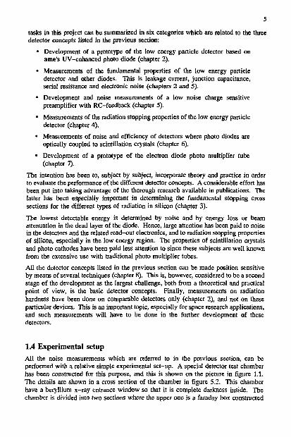
1.4 Experimental setup All the noise measurements which are referred to in the previous section, can be performed with a relative simple experimental set-up. A special detector test chamber has been constructed for this purpose, and this is shown on the picture in figure 1.1. The details are shown in a cross section of the chamber in figure 5.2. This chamber have a beryllium x-ray entrance window so that it is complete darkness inside. The chamber is divided into two sections where the upper one is a faraday box constructed
6
for moderate vacuum. This vacuum is achieved by an adsorption pump. The detector and/or preamplifier under test are placed in this section. The two sections are connected to each other through a heat conducting finger. The lowest section consists of a thermo-electric cooler, whose hot side can be cooled by flowing water through a radiator in the bottom of the chamber. This arrangement allows for moderate cooling of the units under test. A special heat-pump control circuit has been constructed as a NIM (Nuclear Instrument Module) to maintain control of the temperature of the units under test.
A 14 mCi 2 4 1Am source with principal y-encrgy at 59.5 keV has been applied for most of the noise and x-ray measurements. In addition to the heat-pump control the following instruments have been applied: An Ortec model 419 precision pulser, a Tsnnelec TC244 main amplifier, a Tennelec TC953 detector bias supply, and a battery powered Keithlev 485 picoammeter which was put floating on the bias voltage during the leakage current measurements. For measurements of leakage currents below 1 nA the pico-ammeter and detector were placed inside a faraday cage to avoid disturbances from external electric fields. For the measurements of the junction capacitance and the series resistance a Hewlett Packard 4192 LF impedance analyzer was applied. Two different charge sensitive preamplifiers have been used: A conventional Tennelec TC170 preamplifier, and a specially constructed device based on a hybrid Amptek A250. A Nucleus Personal Computer Analyzer with 8000 channels was used as pulse-height analyzer.
The detector chamber in figure 1.1 made it possible to do experiments with a-radiation from a 2 4 , Am source. All other particle stopping measurements where accelerators have been involved are not done at the Department of Physics. Some were carried out at Max-PIanck-institut Kir Aeronomie, Katlenburg-Lindau, FRG, and some at the Swedish Institute of Space Physics in Kiruna, Sweden. The diode processing has been done partly at Center of Industrial Research in Oslo, and partly at ame in Horten. The development of the electron diode photo multiplier tube (EDPMT) prototype, has been a time consuming process. A more detailed description of this work which has been done in cooperation with several external institutions, is given in chapter 7.
Figure 1.1 The detector test chamber which is constructed for moderate cooling and vacuum. The chamber is made at the mechanical workshop at the Department of Physics in Bergen. A closer description is given in section 5.1.1.
7
Chapter 2
The ion implanted silicon diode
The diodes tested in this work are made on n-type silicon with resistivity ranging from 1.5 to 8 kQcm. Their physical dimensions are ISO or ?80 urn thick with circular or square active areas of 33 and 100 mm2. (The active area of the diode is identical to the ion implanted area). The crystal orientation is <111>W and the diodes are processed on wafers with 3 inch diameter. Their rear sides are unpolished (standard lapped). The crystals are grown by the Float Zone technique at Wacker Chemitronics, Munich, FRG. The diodes have been fabricated partly at ame in Horten and partly at ame's division at Center of Industrial Research (SI) in Oslo.
The diodes may be sorted in three groups by the treatment of their active area surface. First, the standard UV-enhanced photodiode which has a thin antireflecting oxide layer covering the active area. Next, the conventional particle diode with a thin Al-layer, and finally the new low energy particle diode (LEPD) with bare surface only. Some of the photo diodes were epoxy coated to get an optimal protection against surface pollutions.
2.1 The fabrication process The combination of oxide passivation, photo engraving and ion implantation has several advantages [Kemmer et al, 1982; Kemmer, 1980]. The S i0 2 passivation layer gives an excellent protection of the pn-junction against pollutions and it is at the same time an effective mask in the ion implantation and diffusion process steps. Concerning diffusion, SiO, is relatively impermeable to several acceptor and donor impurities such as P, B and As [Sze, 1983]. Further, S i0 2 has excellent dielectric properties which makes it a good insulator. The photo engraving technique in the planar process not only enables precise geometrical configurations of the chips but it also makes it easy to change geometry just by changing masks. Ion implantation allows tailoring of asymmetric nearly abrupt pn-junctions resulting in very thin dead layers.
The planar, oxide passivated process applied for these diodes is developed by ame to give optimum properties with respect to low leakage current and high quantum efficiency for UV-light. This implies a shallow diode entrance window or dead layer.
w The <111> axis is perpendicular lo the surface of the diode.

8
which, as mentioned, is of fundamental importance for detection of low energy particles. As an example the fabrication of the UV-enhanced photo diode which is used as basis for the LEPD, will be described schematically. This process can unfortunately not be referred in details as it is proprietary to ame.
2.1.1 Lithography, oxidation and doping
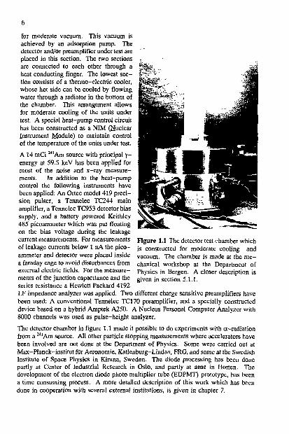
The lithography processes are done with UV-light and the proximity exposure method. In this method a small gap, 10 to 25 um wide, is maintained between the wafer and mask during exposure. This gap minimizes mask damage, and the approximately 2-4 urn resolution which is achieved by this method, is good enough for the relatively simple geometry of these masks. The chrome masks needed for the UV enhanced photo diode and the LEPD, shown schematically in figure 2.1, are produced by Align-rite, Wales, UK.
Mask 2: Mask 3:
I All dimensions in microns
Figure 2.1 Schematic illustration of the LEPD fabrication masks. Mask 1 defines the active area, mask 2 the contact hole, mask 3 the contact ring and bonding pads, mask 4 the particle entrance area, and mask 5 the polyimide coated area.
Two oxidation processes are performed during the fabrication of the UV-enhanced photo diode. The first results in a thick oxide layer. This oxide covers the whole front side of the finished diode except from the active area where it is removed as described below. On the back side this oxide is removed prior to the predeposition and diffusion of phosphorus which results in the back n* contact. In the second oxidation process an antireflection oxide layer is grown over the active area of the diode. T.e thickness of this layer matches the desired spectral response [Hansen, 1985].
The front p* layer is defined by implantation of boron. The wafers are installed tilted during the implantation process so that the ion beam is incident 7 degrees to the direction perpendicular to the surface. This is done to prevent any channelling effects along the <111> crystal axis. Subsequent to the implantation step annealing and gettering are performed.
2.1.2 The UV-enhi-.i.-ed photo diode
The first three masks in figure 2.1 are needed to make the UV-enhanced photo diode. Mask 1 defines the active area of the diode, that is, where the thick oxide layer is

9
removed. Hence, the thick oxide will act as a mask during boron implantation and only the active area will be implanted. The active area is about 100 mm2 as the diameter of this mask is 11.4 mm. Mask number 2 defines the hole for the contact ring through the antireflcction oxide to the implanted boron layer. This hole is lOum wide with 25 urn separation from the thick oxide. The contact to the implanted boron layer is formed by evaporating a 1 (im thick aluminum layer onto the diode front side. Mask number 3 defines the pattern of this contact and the bonding pads. The contact is then a 40 urn wide ring around the perimeter of the diode, that is, 15 fim Si0 2 on each side of the contact hole will be aluminum coated too. Four square bonding pads of size 125x125 jim2 are placed with 90° separation on the inner extension of the contact ring. An 1 u,m aluminum layer is also evaporated onto the diode n+ layer to form the back side contact.
2.1.3 Annealing and gettering
There are two annealing processes involved in the fabrication of these diodes. The purpose of the list of these, which is done next to evaporation of aluminum, is to get an optimum Si/AI-contact. This is done at 460° C in forming gas (about 90% N 2 and 10% HJ. The purpose of the first annealing, which is done next to implantation, is to restore the crystalline structure which is damaged by the implantation, and to achieve full acceptor (or donor) activity. Gettering is done to reduce contamination levels and trap impurities. The gettering action requires three physical effects: (1) the release of impurities, (2) the diffusion of the impurities to a capture zone, and (3) the capture of the impurities at some sink. To achieve good gettering, all these three mechanisms must be operative.
To fabricate a diode with low leakage current, that is, a low noise diode, the gettering processes are very important and have to be efficient. The n + layer on the diode back side will be the capture zone, and the phosphorus will act as the sink, ame has developed an efficient annealing/gettering process in N 2 environment. The annealing is done at a relatively high temperature so that the majority of the implanted acceptors are activated. Details cannot be given due to ame proprietary rights.
2.1.4 Bonding
The wafers are scribed and divided into separate chips which arc tested, sorted and prepared for the bonding. Each chip or diode is normally mounted on a printed gold film on a ceramic substrate. The diode is attached to this gold film by a conducting epoxy resin. The ceramic substrate contains two feedthrough pin connectors on each side of the diode. One of these is ball bonded to the gold film and the other to one of the four bonding pads on the diode surface contact ring. Gold wires with 3-5% elongation and 25 um diameter are normally used, but aluminum wires and wedge bonding may also be applied. The choice of bonding technique and material depends upon the application of the diode.
2.1.5 Modification of the photo diode into a particle detector
A 280 urn thick UV-cnhanced photo diode with circular active area and 4 kQcm bulk resistivity, was chosen as basis for the low energy particle diode (LEPD). One more processing step is needed to modify the photo diode into a LEPD. The thinnest possible deadlaycr is obtained by removing a part of the antireflcction oxide. Mask 4 in figure

10
2.1 defines the particle entrance area which has a diameter of 9.1 mm (-65 mm2 area). This area is smaller than the active area in order to maintain a good protection of the pn-junction. The selected part of the implantation oxide is etched away in 5% buffered hydrofluoric acid. Any oxide left after this process will be native oxide only, that is, about 3 nm thick.
2.1.6 Polyimide coating
The idea with the polyimide coating is to give a better surface protection of the diode pn-junction. The polyimide will act as a getter and is especially efficient in trapping alkali metal molecules. These are especially harmful to the diode and will cause an increase in the surface leakage current. This polyimide coating is believed to be especially important for the diode in the new Electron-diode Photo-multiplier-tube (EDPMT) as this diode will be exposed to an extra large amount of alkali metal vapor. This is because the fundamental ingredient in the photo cathode is cesium or another alkali metal. One drawback with the polyimide is its high ability to absorb moisture, which may cause an increasing leakage current. Hence, the mission of the polyimide is lost if the diode is used in a humid environment. This problem is avoided for the diode in the EDPMT or other closed system applications.
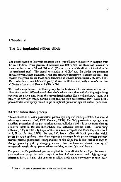
The Selectilux HTR3 polyimide applied here is photosensitive and is during fabrication ^ „ _ treated like a negative photoresist until the — t u Gå— development. The area to be coated is • "^ •— •— ' • defined by the pattern of mask 5. Except from four 125x125 (un2 holes over the bonding pads, this mask is identical to the g^igjgiji^^l inverse of mask 4. The polyimide is • = , . , . . . _ ., ,—, imidized for 60 minutes at 350°C in vacu- S o ^ L n « h i„ m n ! urn. The temperature is ramped slowly up D S ' - ° X i d e D S l b u l k H n +
and down to and from 350°C. The rampe rate depends upon thfi vacuum furnace that Figure 2.2 Schematic cross section of is applied. The result is an about 1.8|un the low energy particle diode (the bond-thick layer of polyimide. A schematic cross ing pads are not shown), section of the LEPD is shown in figure 2.2. This cut does not show the bonding pads and the holes in the polyimide layer over these.
22 Process simulation
The diode fabrication is a detailed, costly and time consuming process. Computer simulation of the process is a useful tool which can be used to determine the influence of changes in the different process parameters on some of the diode properties. However, the most important property of the diode, the leakage current, cannot be determined by simulation. This is because it is too complex to give a description of the influence of the different process parameters on the physical phenomena causing the leakage current.
The most interesting information available from simulation is the impurity profile

11
subsequent to each processing step. The resistivity and thickness of implanted and diffused layers can be found from this profile. For the diode described here, it is of particular interest to determine the profile of the implanted boron. This will give a good indication of the thickness of the diode's dead layer. The influence of changes in the implantation energy and dose, will also be found.
The annealing and gettering processing step will, of course, affect the implanted boron profile. But this processing step is, as mentioned, optimized to achieve a low leakage current, and it is therefore of no practical interest to probe the effects of any changes in temperatures and time periods involved here.
2.2.1 Simulation results
The SUPREM III (Stanford University Process Engineering Models) simulation program which are used here is not the most advanced. However, SUPREM III allows among other things simulation of the oxidation/drive-in and ion implantation processes which are necessary to determine the implanted boron profile and the sheet resistance. The implanted boron profile are, before annealing, described by a modified Pearson type IV distribution, and the sheet resistance is calculated as the reciprocal of the average conductivity of the implanted layer [Antoniadis et at, 1978].
10 "i
1 0 "
1 0 "
Relative change in £T-^~. implantation dose: • ' " " - - r ^ v +44S
' • • . X o% \ S \ _ 4 4 %
10
10
10 1 0 •"• ••K " 1 0
10 , 5 \ §10
10 "• \ F J 1 0
10 "• \ 10 i n
1 0 c 50 100 150 20 SILICON DEPTH [nm]
0 W
Figure 23 Simulated net impurity concentration versus depth (from the silicon surface) and relative change in implantation dose. The bulk phosphorus concentration is about 10 1 2 cm"3.
Relative change in implantation energy:
+10% +5% 0% -6%
<" \ \ -10%
\ V \ \
50 100 150 200 SILICON DEPTH [nm]
Figure 2.4 Simulated net impurity concentration versus silicon depth and relative change in implantation energy. The n-bulk concentration is about 1012cm"3.
The net impurity concentration profile subsequent to the annealing and gettering procedure is shown in figure 2.3 and 2.4. The n-type bulk concentration is about 1012cm~3. These figures indicates how changes in the implantation dose and energy respectively, affect the doping profile. The changes are given relative to the values adopted by ame in their "standard" process described in the previous section. The absolute values can, due to ame proprietary rights, unfortunately not be given. The junction depth, that is, where the chemical concentrations of implanted boron and predoped phosphorus are equal, is Xj-175 nm for the "standard" procedure. The thickness of the p* layer will be Xj-xp, where x p is the depletion width of the pn-junction's p-side. The doping profiles in figure 2.3 and 2.4 will therefor give a good indication of the p* layer thickness even

12
though x p depends on the actual boron concentration, too. Simulations where the n-bulk resistivity, p, was increased step-wise from 1 to 10 kSicm resulted in almost identical doping profiles. The only difference was in their upper tail where the junction depth, Xj, increased from 172 to 176 nm as a result of the decreasing n-type bulk concentration.
For the LEPD there are two aspects that have to be considered if the implantation dose or energy is to be altered. First a shallow deadlayer is desirable to keep the corresponding particle energy loss as low as possible. This implies a shallow depletion depth, x f. Next, low p* sheet resistance is important as there will be no conducting metal layer on top of the p* layer. This implies a high boron concentration in the top of the p* layer. Again it is assumed that the majority of the implanted boron is activated during ames efficient annealing procedure.
It is clear that changes in the implantation energy have the largest influence on Xj. The junction depth varies from X|~191 nm to Xj~148 nm for the examples shown in figure 2.4. The boron concentration drops, at the same time, one order of magnitude giving a corresponding increase in the p* sheet resistance. From figure 2.3 it can be seen that the junction depth is hardly altered at all by changes in the implantation dose (from Xj-178 run to x—170 nm). This result is as expected since the range of the implanted boron ions is determined by their energy and not their dose. The variation in x> with the implantation dose is due to difference in diffusion during the high temperature processing steps only. The conclusion is that to realize a shallower deadlayer without any reduction in the resistivity, the implantation energy has to be lowered while the implantation dose must be raised.
These simulation results should, however, be considered with a critical mind as the simulation program, unfortunately, contains some bugs. First, these became evident in a few occasions where weak changes in the input parameters caused large, unrealistic jumps in the output data. Late, there was found a large deviation between the measured p* sheet resistance (section 2.3.2) and that calculated from the simulation results. The latter was about 10 times larger. A possible explanation of this is an error in the calculation resulting in a too low boron concentration. Due to this no attention will be paid to the simulated p* sheet resistance, and the doping profiles shown in figure 2.3 and 2.4, must be considered as instructive only.
2 3 Electrical properties of the diode The silicon diode described in section 2.1, may to a large extent be regarded as a condenser in series with a resistor when used as a nuclear radiation detector. The fundamental electrical factors are then the junction capacitance, Cj, the leakage current, I,, and the series resistance, R,d. The junction capacitance is often simply referred to as the diode capacitance and the leakage current of the diode as the dark current. It will be shown in section 5.2 that if these factors are known, the total electronic noise of the diode may be calculated. Further, many of the diode properties with respect to detection of both x-rays and particles, may be predicted from knowledge of R,a and Cy
Measurements of C,, R„ and I, are therefore the first step in an evaluation of a diode as a radiation detector. The results of such measurements on one of the new LEPD devices

13
50 100 150 Reverse bias [V]
Figure 2.5 Measured leakage current, I„ junction capacitance, Cj, and series resistance, R r f, versus reverse bias of a LEPD at room temperature.
are displayed in figure 2.5 c ). Throughout this work the diodes will be operated in photo conductive mode only. A reverse bias, V R , is then applied to the pn-junction so that the front p* layer is put to the lowest potential.
2.3.1 The junction capacitance, Cj
The pn-junction may be regarded as a parallel plate condenser where the distance between the two plates is the depletion width, x„, that is, the distance between regions where the incremental charge appears. The capacitance per unit area is then given by the dielectric constant, E a, divided by x„. Due to this very simple relationship between Cj and x w l measurements of C, can provide useful information about the nature of the impurity distribution [Grove, 1967]. The depletion width may be expressed as [Leo, 1987):
x-x+x-
eN, 1+-N A
ifstv^U. eNjl+—i
N„
2ep eN, '(W*) (2.1)
The noise properties of this LEPD are shown in figure 5.S.

14
where x„ and x p are the depletion widths into the n and p region, respectively. Next, V 0
is the built-in voltage across the pn-junction, N D the predoped phosphorus concentration of the bulk, and N A the implanted boron concentration in the p* layer. It is assumed that all the impurities are electrically active. The approximation in this equation, which is called the one-sided-step approximation, is very accurate since N A generally is much larger than N D for a p*n diode. For the LEPD, N A -10 6 N D which makes x.-lO'x,, so that xw~x„. The result is a one-sided step junction which would be more clearly visualized in figure 2.3 and 2.4 if their Q, axes were linear and not logarithmic. An expression for the junction capacitance is easily derived from equation 2.1. It is, however, more interesting to look at the inverse square junction capacitance and it's relation to the reverse bias:
J_ C, 2 e«A.eN, -(v (2.2)
Here Aj is the active pn-junction area. The capacitance of the LEPD which is plotted versus reverse bias in figure 2.5, was measured on an HP4192 LF Impedance Analyzer at 100 kHz. Because this analyzer provides maximum 35 V reverse bias, a Tennelec TC908 Bias Supply was used for voltages above 35 V. The diode was then connected to the analyzer through a large (2 uF) decoupling condenser.
The plot of 1/C? versus V B in figure 2.6 verifies the validity of the one-sided-step- junction theory for the LEPD. The curve can with good accuracy be represented by a straight line in the low re verse bias region where the depletion width increases with increasing V„. When the diode is depleted the plot can be represented by a new straight line as the capacitance has reached its minimum and becomes approximately constant. The depletion voltage is defined as the reverse bias at the intercept of these two straight lines. This is illustrated in figure 2.6. Optimum noise properties are, however, often achieved at a somewhat larger reverse bias where C, and R ! d reach their minima. This will be shown in chapter 5. The depletion voltage of the LEPD is about 45 V while the reverse bias which gives minimum capacitance and optimum noise properties, is about 60 V. This can be seen from figure 2.5 and 2.6, respectively. Note that the predicted values of x„ and 1/C? in equation 2.2 and 2.3 respectively, have some deviation from their real values in the intermediate region around the depletion voltage. This can be seen from figure 2.6.
By inspecting equation 2.2 and the straight line plot of 1/C? against V„, more information about the diode can be found. The slope of this curve yields the doping
5 0 100 Reverse Bias
Figure 2.6 Illustration of the linear relation between Cj 2 and V„ (reverse bias) for the LEPD based on the measured capacitance also plotted in figure 2.5.

15
concentration of the bulk, N D , and the built-in voltage, V„, can be found from the Y-axis intercept where VR=U. Once N„ is found, the bulk resistivity, p, can be determined. Figure 2.7 shows a plot of the relationship between N„ and p for n-typc silicon at 300K [Sze, 1981]. For the LEPD V0= 0.66V and N D =110 1 2
cm"3, resulting in a resistivity of p=4 kQcm.
2.3.2 The series resistance, R^
10
o 10
\ ,. \ \
\ \
— 1 1 [kn 10 The major contributions to the total series
resistance of the planar ion implanted diode are the resistance of the undepleted silicon bulk and the series resistance of the p + layer. The resistance in the diode contacts are kept neglibile due to high doping concentrations (n* and p*) and efficient annealing subsequent to the aluminum evaporation. The total series resistance for a circular p*n diode with a line contact around the perimeter of the p* layer, was found by Rawlings and Deighton [1989] to be:
Figure 2.7 Impurity concentration versus resistivity in n-type silicon at 300 K [Sze, 1981]. The dashed line represents extrapolated data.
1 R , G„ 25
(2.3)
where G„ is the quasineutral silicon conductance, that is, G;1 is the effective series resistance of the undcpletcd n-bulk. The above equation is valid for frequencies up to [4nCj(G;'+R l h/25)]_ 1 in the case of the circular diode. Further, R l b is the sheet resistance of the emitter, that is, the p* layer. The emitter contribution to R s d does not depend on the radius of the noncontacted emitter region. For a square diode R l d equals R ! h/24.
The Revalues plotted for the LEPD in figure 2.5, was measured on an HP4192 LF Impedance Analyzer at 100 kHz up to 35 V reverse bias. Above this bias G„ has been calculated from the capacitance measurement according to the following relation:
G;'-P- (d-x n)-p ( !_. ! • Ar " A C
(2.4)
where d is the thickness of the n-bulk. The exact value of d is found from the minimum value of Cj at full depiction. The expression for x„ has been derived from the definition of Cj. The contribution of the emitter sheet resistance to R r i is from this found to be 22.5 £2. Four-point-probc measurements directly on the surface of some other LEPDs of the same batch confirm this as the emitter sheet resistance is measured to be R l h-590 Qfcj. The contribution to R ! d is then, according to this and equation 2.3, about 23.6 £2. Ballistic deficit due to the emitter sheet resistance and it's influence on

16
the noise properties of the diode is found to be neglibile, but this will be discussed in chapter S.
For a conventional particle diode with a metal covered surface, the only contribution to R,j should be the resistance of the undepleted n-bulk. The contribution from the emitter or the p* layer will be of the order of a few mQ only. This is confirmed by measurements on a square diode with a thin aluminum layer on top of the emitter.
2.3.3 The leakage current, i,
The leakage current is the most difficult parameter to control during the diode fabrication process. The average leakage current in a batch has been greatly reduced during the last years due to improved gettering and passivation techniques. The leakage currents of the different devices within a batch may, however, vary a lot. The LEPD which leakage current is plotted in figure 2.5, is a relatively good device. A Keithly 485 Picoammeter is used to measure I„ and the reverse bias is supplied by a Tennelec TC953. The temperature dependence of the leakage current and its influence on the diode noise, are treated in section 5.3.2.
The leakage current is due to thermal generation and recombination of electron hole pairs somewhere in the active volume of the diode. It is convenient to separate the total leakage current, I„ into two parts; the bulk leakage current, I,„, and the surface leakage current, I l s. For the bulk leakage current the thermally generated carriers may recombine directly or through recombination centers as explained in section 2.4. For the ame diodes the density of such centers are kept relatively low by the efficient gettering process. The bulk leakage current of this p*n diode may be expressed as [Sze, 1981]:
x . N„ (2.5)
where D p is the diffusion coefficient of holes, x p the hole life time, n the intrinsic carrier concentration, and x c the effective life time of the carriers. The first term inside the brackets is the diffusion current which is due to electron hole pairs generated outside the depletion region, that is, in the neutral p or n side of the diode. The second term, the generation current, is due to electron hole pairs generated inside the revers^ biased depletion region. For silicon with relatively small intrinsic carrier concent:,; n (ni=1.4510'°cm"3 at 300K) the generation current will be the dominating at rooii. temperature [Sze, 1981]. Hence, the bulk leakage current is to a good approximation proportional to the depletion volume, that is, ^«x^-Aj.
The surface leakage current, I u, is due primarily to charges which is in or outside the oxide on the diode surface and induce image charges in the semiconductor, and thereby cause the formation of surface channels and surface depiction layer regions. The composition of I„ is complex as it depends on many factors including surface chemistry, the existence of contaminants, the surface surrounding atmosphere, the type of mounting, etc. Clean encapsulation is generally required to minimize this I„, and the SiO, passivation layer gives a good protection of the surface pn-junction. This is the function of the polyimide coating too, if it is not exposed to an humid environment. An epoxy coated surface will give the best protection of the pn-junction against external

17
pollutions. Epoxy coating is, however, impossible to apply on the LEPD and other diodes where the radiation must enter with minimal absorption or attenuation. It is difficult to give an expression for I u, but the possibility of the formations of surface channels is, to a first approximation, proportional to the circumference of the active area.
The separation of the total leakage current, I„ into two parts is demonstrated in figure 2.8. The bulk leakage current, I,,,, and the surface leakage current, I,s have been measured on an ame AE9441 UV-enhanced photo diode with guard ring. The processing parameters of this diode is analogous to those of the LEPD and the results of the leakage current measurements should thereby be adoptable for the LEPD. The guard ring diode has a separate contact ring outside the p* contact ring. These rings are put the same potential and the contribution of I,b to I, is found by measuring the current through the p* contact ring. The current through the guard ring is, to a good approximation, equal to 1& It is clear from the figure that the surface contribution is nearly twice the bulk contribution at and below depletion voltage. This is the region of largest interest, so the increase in I l b at higher voltages does not play any important role. The surface of this guard ring diode was protected with an epoxy coating. This means that the unprotected surface of the LEPD may give an even larger contribution to I,.
2.4 Charge generation and recombination in silicon The intention here is to give a brief description of the generation and recombination processes taking place in silicon. The details can be found elsewhere [Grove, 1967; Sze, 1981]. When the electron hole pairs are generated inside the depletion region of the diode, they will be separated and swept in opposite directions by the dipolc field. To contribute to the output signal, a carrier has to move completely across the depletion region. In the neutral p and n regions, only the minority carriers can contribute to the output signal because the majority carriers will be repelled out of the depiction region by the electric field once they diffuse into it. Minority carriers are, on the other hand, accelerated across it.
When silicon is exposed to radiation, carriers are generated mainly by band-to-band transitions (intrinsic), but also by transitions involving forbidden-gap energy levels
1 0 ' <
a v
o
bfllO ' cd
' L L ' 1 1 1 1 1 1 1 1 1 ' ' ' •
/ ^ -'—(i
K / " "
^ -f " , - - * Mb
j . A
/ A
0 2 0 40 60 80 100 R e v e r s e b i a s [V]
Figure 2.8 The composition of the total leakage current in a guard ring diode at room temperature. This diode is, except for the guard ring arrangement, fabricated the same way and have the same specifications as the LEPD in figure 2.5.

18
(extrinsic) due to intermediate centers. Altogether a mean energy of 3.61 eV is needed to excite an electron across the bandgap and thereby create one electron hole pair in silicon at 300 K. About % of this energy is transferred to the lattice in form of phonons as the corresponding bandgap energy in silicon is only 1.12 eV.
Electrons in the conduction band and holes in the valence band may recombine directly band-to-band or through intermediate centers. Band-to-band recombination may be considered as the opposite to intrinsic generation, and the excess energy will be emitted in form of light or heat, or transferred to another free electron or hole. The latter is called the Auger process which occurs when electrons are injected into a heavily doped p* region or when holes are injected to a heavily doped n* region [Sze, 1981; Dziewior etal, 1977].
Recombination through intermediate centers can be described by four processes: electron emission, electron capture, hole emission, and hole capture. This is electrons moving between the conduction band and the centers, and holes moving between the valence band and the centers, respectively. The intermediate centers disrupt the perfect periodicity of the crystal and thereby introduce energy levels in the forbidden gap. The centers are imperfections within the lattice which may be due to impurities (foreign elements), radiation damage causing lattice defects, or surface states.
The surface states are irregularities associated with the surface where the lattice is terminated and the density of levels within the forbidden gap is large. Hence, the recombination rate is enhanced near the surface with the result that the excess carrier density will be smaller there. This will result in a diffusion of carriers from the body of the diode towards the surface. An additional complication may occur if, for example, positively charged ions are present on the diode surface (oxide) of the p + region. Holes will then be pushed away from the surface and electrons will be attracted there. This gives rise to a surface space-charge region as the charge neutrality no longer holds there. The result is an increased movement of generated carriers towards the surface where they recombine. Recombination due to these surface effects is called surface recombination.
2.5 Diode stability It is important that a detector remains as stable as possible in the environment where it operates. The silicon diode has, compared to detectors with internal gain, very low temperature drift in the amplitude of the output signal, [ts noise properties have, as will be shown in chapter 5, a stronger dependence on the temperature. The naked surface of the low energy particle detector (LEPD) makes this device sensitive to surface pollutions. F-posure to ether vapour for instance, gives rise to an increase in the leakage current. It is, however, possible to restore the conditions prior to exposure by baking the detector at 140°C in dry air for 48 hours or more. The leakage current of the tested LEPDs are, however, relatively stable if the detectors are stored in a closed box containing silica gel.
19
2.5.1 Radiation hardness
Radiation hardness is an important topic in all applications where the instrumentation is exposed to high radiation levels. No radiation hardness measurements have yet been performed on the low energy particle diode (LEPD) prototype. This is mainly because other experiments related to radiation stopping properties and noise properties have been given the highest priority. Some results from radiation hardness tests on comparable detectors are, however, available. These are detectors made on the same type of material from the same manufacturer, and with almost similar fabrication techniques concerning doping, passivation and gettering.
Some cryogenic detectors made at ame were tested to a total dose of 30 krad* without being measurable damaged [Hansen, 1990]. Each of these detectors had four 24 mm 2
active areas, they were 280 urn thick and made on 100 Qcm material. At Center for Industrial Research (SI) in Oslo a 300 urn thick capacitively coupled microstrip detector containing 257 diodes, each 39 mm x 25 urn was exposed to electrons from a "Sr source and given a total dose of 830 krad over 25 days. The increase in leakage current was observed to be 0.02 nA/(cm3rad) [Dijkstra et al, 1988], This microstrip detector was made on 4 k£2cm material.
A test chip containing gated diodes with 0.25 mm 2 active area, also fabricated at Center for LJMstrial Research (SI) in Oslo, was exposed to x-rays from a "Co source. A 100 um wide Al gate on top of a 500 nm oxide surrounded the active area and made it possible to separate the contribution of bulk damage and surface damage. The diodes were reverse biased to 60 V during exposure. After a total dose of 2.8 Mrad the surface generated current increased by a factor of 100 while the bulk generated current was less than doubled [Ferguson et al., 1990].
These results are relatively good compared to detectors fabricated by others [Dijkstra et ai, 1988]. It is, however, difficult to give a general prediction of the dose a detector on board a satellite will be given. This is strongly dependent on the satellite's orbit and life-time, and on the thickness and construction of the detector housing. Values between some tens to a few hundred krad is, however, not unusual.
These results are of course not fully adoptable for the LEPD. They should, however, give a good indication of the radiation hardness performance that can be expected for this material and these processing techniques.
* 1 rad= 10 ml/kg. In silicon this is equivalent 10 about 1.45-10* MeV/cm1.
20
Chapter 3
Radiation stopping in silicon
Key words for a detector used for radiation energy analysis are efficient attenuation, absorption and charge collection, and finally good energy resolution. The attenuation efficiency of a silicon diode is mainly determined by diode's thickness. The fraction of attenuated radiation that is absorbed in the sensitive detector volume depends, in addition to energy lost by secondary radiation effects, on reflection and energy loss in the surface of the diode. The charge collection efficiency which will be discussed more detailed in chapter 4, is close to unity in the depleted volume and then decreasing considerably towards the surface of the diode. The energy resolution will be treated in chapter 5. All these effects are more or less dependent on the nature of the radiation. The ideal detector should have 100% radiation attenuation and absorption, uniform charge collection efficiency of unity, and 0% energy resolution.
To evaluate the ame silicon diode as detector for low energy radiation, it is first necessary to look at its properties with respect to attenuation or stopping of the various types of radiation. For the three detector concepts listed in chapter 1.2 detection of scintillation light, X-rays and particles have to be considered. There are a lot of valuable data published on radiation stopping in silicon which are advantageous to use in the evaluation. The relatively light protons and He* ions and the somewhat heavier O* ions will be taken as examples for the particle stopping properties of the diode. Concerning electrons, most attention will be paid to the low energy region, since that is of particular interest for the Electron-diode Photo-multiplier-tube (EDPMT). This evaluation will proceed in chapter 4 where influence of the low energy particle diode's dead layer on the different types of radiation, will be discussed.
3.1 Sensitivity to light A combination of a photo diode and a scintillation crystal is, as mentioned in chapter 1.2, a possible detector for high energy x-rays. The radiation stopping efficiency in this configuration is determined by the crystal type and dimensions. The most interesting feature about the diode in this connection is how it's spectral response matches the emission spectrum of the crystal. Here it is most convenient to express the diode's spectral response by its quantum efficiency, Q e , and the dependence of Q e on the wavelength. For each wavelength Q e is defined as the average number of electron hole

21
pairs created by absorption of one photon. The composition of Q e is relatively complex [Wilkinson et at, 1983], but it may be understood simply as bow effective the energy of the incident light is transferred into electric charge at the preamplifier input. The limiting factors are reflection and absorption of light in the surface coating(s), absorption of both light and photo-electric charge in the p* dead layer. The latter will be discussed more detailed in section 4.1 as the problem is very similar to that arising in detection of low energy particles.
The quantum efficiency, Q e , of two ame UV-enhanced photo diodes, AE987 and AE9871, are shown as function of wavelength in figure 3.1 [ame, 1989]. The only difference between these diodes is that the AE9871 device is epoxy coated 0 . Both of them have a 200 nm thick S i0 2 antireflection layer. The cutoff at about 300 nm for the AE9871 diode is due to absorption in the epoxy coating. The peaks of Q e in the UV-region of the AE987 diode are due to maxima in the Si0 2 transmission coefficient. For perpendicular incident light these maxima will occur when the SiO, thickness is equal to mA/4n 0 l where m=l,3,5 X is the wavelength and no, the refractive index of the oxide [Hansen, 1985]. The spectral response of the diode can in this way be fitted to wavelength just by controlling the oxide thickness.
A diode connected to a scintillation crystal device. This is because there has to be some kind of transparent medium between the crystal and the diode to minimize the light loss. This may be an cpoxy coating, some kind of optical grease, or a combination of these. Anyway, it should be realistic to obtain a Q e of about 80% for wavelengths between 300 and 950 nm.
3.2 Stopping efficiency for y- and x-rays The interaction of y- and x-ray photons with a semiconductor takes place through three principal processes; the photoelectric effect, Compton scattering and pair production. The influence on attenuation of these three processes dominate other phenomenas such as photo nuclear reactions which therefore are neglected. The interaction of y- and X -rays with matter is considerably different from the particle stopping processes. A particle looses energy continuously along its track while a photon in a beam disappears once it undergoes an interaction. As a consequence, the number of photons disappearing from the beam will be proportional to the thickness, x, of the absorber. The intensity,
200nm SiO a
+ epoxy coat ing ; 400 600 800 1000
A [nm] Figure 3.1 Spectral response of a photo diode (ame AE987) with a 200 nm thick antireflection layer (solid line), and the additional effect of an epoxy coating (ame AE9871, dashed line).
1 will have a Q similar to that of the AE9871
EPO-TLK 301-2 optically transparent epoxy

22
I, of a beam whose whole cross section is covered by the absorber, is defined as number of photons per second, and can for a monochromatic beam be expressed as:
I-I 0e"i" (3.1)
where I„ is the initial intensity of the beam and u the linear attenuation coefficient. In this case u is made up additivety of the linear attenuation coefficients of the photo electric effect, Compton scattering and pair production, -c, o and K respectively.
3.2.1 The interaction processes
In the photoelectric effect the interacting photon gives its entire energy, E,,,, to an atom resulting in ejection of an electron with energy E^-E^, where E^ is the binding energy of the electron. This process is strongly dependent on the atomic number; xi*Z5, and the photon energy; fxEj;". The Compton effect may be considered as an elastic collision between the photon and an electron. The wavelength of the scattered photon is increased as it loses a part of its energy to the electron. How much depends on the deflection angle. The Compton total attenuation coefficient, a, can be divided into two components; o a and a s , the Compton linear absorption and scattering coefficients respectively. This is because only a fraction (oja) of E^ is transferred to the electron and hence absorbed, while the remainder is scattered without absorption11. If Rayleigh scattering, which is elastic scattering with the absorber atoms, also is considered the dependence on atomic number and photon energy is approximately (o+o r )«Z and (a+o r)aE;J. Here o r is the Rayleigh scattering coefficient. In pair production which occurs only in the field of a charged particle, normally the nucleus, all the photon energy is lost and an electron-positron pair is created. The minimum energy needed to this process is the sum of the electron and positron rest energies (1.02 MeV), an eventual excess energy is shared as kinetic energy by the electron and positron. The dependence on Z and E,„ is KOCZ2 and K«ln E,,,.
3.2.2 Total attenuation
The composition of the total attenuation coefficient for silicon, u, is shown in figure 3.2. The theoretical values which is represented by lines, is taken from tables calculated by Storm and Israel [1967] who have considered the Compton electrons as bound electrons. Also plotted are 13 different experimental data sets of |i collected by Salomon et al. [1988]. The total absorption coefficient, n a , is due to energy dissipating processes only, that is, the Compton and Rayleigh scattering coefficients, a s and a p are not included. Figure 3 3 shows a pulse height spectrum from a " 'Am source collected with a LEPD. The principal y-ray emission of this source is at 593 keV where the influence of the photoelectric effect and Compton scattering are about equal (T=0 .28 cm"1 and a=0.35 cm"1). The 59.5 keV photo peak caused by the photoelectric effect is superior to the peak caused by back scattered Compton photons, most of which escape the detector.
0 It is assumed thai all the electron energy is absorbed within the detector while the scattered photons escape the detector. Some electrons may, however, escape the detector since their range in many cases may be comparable with the silicon diode thickness. On the other hand, some of the scattered photons may interact within the detector and deposit energy. Hence, a a and o s must be considered as guiding only.

23
Compton recoil electrons from head-on collisions will have maximum energy transfer from the incident photon and give rise to the Compton edge. The other peaks in the spectrum are due to N p X-rays.
" 'Am Photo — ft peak
2400-
iaoo-
Compton edge
i
80D-\ B a c k -1 s c a t t e r \ peak
0 lb m ' 30 40 so'' ft E P h [keV]
D 70
Figure 3.3 Room temperature M 1 Am energy spectrum collected with a LEPD connected to an Amptek A250 preamplifier.
The relative attenuation, l-(Wo), of a photon beam in silicon slices of varying thickness is calculated as function of energy and plotted in figure 3.4.
" l o * * ' " i " " 1 — »"—• ' " " " ' — • ' i ' " 1 1 1
r e \ K-edge: 1.839lceV : e \ \ Average K X—Ray \ energy: l.75kev r
: fl „ , •
<D 10 •- r
o
« 1 0 1 o \ \ 13 ' 1 \ \ O : ^ " V W M 3 " <••" ^ \ ^ ^ (010 ' i / vV*« ' O v S,n / y'\ "*»?*'« •£10 "l (0 :
11
3 1 0 " ' - 1 i i l iuii i—rnTinr i— i i iinlrj ' 1 1IIUUI—rTTtnfi 1 10 10« 10 * 10 ' 10 *
Eph [keV] Figure 3.2 Total linear attenuation coefficient in silicon versus photon energy. The lines represent theoretical values [Storm and Israel, 1967], and the circles measured values [Salomon et al, 1988].
Note that the fraction of beam energy absorbed in the slices is somewhat less than this.
1.0 -
0.8 -
-" —'—'—
\ \ ^
O - V V ^ ' N \ \
-
-0.6 -) -0.4 • ; 'f \
9\ SA (Ar* tera r\<S
\ VA V* <* > \ \ \
\
0.2 -
^ \ ''• x \ ~
0.0 -1 J i i i • f i t 1 1 S ~ 1 10 100 1000
E P h [keV] Figure 3.4 Relative total attenuation, (I-I/y, and transmission, I/Ig, plotted against photon (x-ray) energy. Attenuation data taken from Storm and Israel [1967].

24
Secondary or scattered radiation from any of the interaction processes may escape (photons) or be partly absorbed only (electrons). The energy loss due to these effects increases as the photon energy increases. Silicon diodes are generally considered to be poor v- and X-ray detectors due to the low Z-number and thereby low attenuation. For the 280 urn LEPD more than 50% of the beam is transmitted for photon energies above about 15 keV. This can be seen from figure 3.4 where the beam attenuation in germanium, sodiumiodide and lead are also shown for comparison. At low energies, however, the low attenuation in silicon becomes an advantage due to low loss in the dead layer present in all solid state detectors. To conclude, the LEPD should be an excellent detector for low energy y and X-rays [Jaklevic et al, 1988], The upper energy limit is set by the diode thickness and the beam flux. For the 280 um LEPD this limit is around IS keV for low flux applications. For large fluxes which compensate for low attenuation, however, this device can be used to detect y-radiation with energies up towards 1 MeV. The low energy limit, on the other hand, will be determined by the system noise which will be treated in chapter 5. In this energy range the photo electric effect is the dominant interaction process, as can be seen from figure 3.2. Here all the energy in the attenuated beam will, to a very good approximation, be absorbed.
3.3 Stopping power of protons and ions
The slowing down of protons and charged ions in solid targets is essentially due to interactions with the nuclei and the electrons of the target. Other effects, such as production of nuclear reactions and energy losses due to radiation effects, are not dealt with here, since their contributions are negligible in the energy range considered in this work. The total rate of energy loss as a function of distance, the total stopping power, is then the sum of the nuclear and electronic components, (dE/dx),=(dE/dx)n+(dE/dx)e.
It is also convenient to separate the total stopping power into three velocity dependent regions as shown for a typical amorphous target in figure 3.5. In region I the stopping power is a decreasing function of velocity and is almost entirely due to electronic collisions. The stopping power is here given by the well known Bethe-Block formula [Bethe, 1930; Bloch, I933] which is valid for particle velocities above v^VoZ, 2 0, where v„ is the Bohr velocity and Z, is the ion atomic number. The stopping power has a maximum in region II, just above v,. In region HI, below v„ the electronic stopping power is approximately proportional to the particle velocity. Here the nuclear stopping power will also contribute to the total stopping power as shown in figure 3.5. This contribution will increase with increasing ion
mass. The total stopping power is here, to a good approximation, given by the LSS theory [Lindhard, Sfharff and Sfhiøtt, 1963].
NUCLEAR STOPPING
B r T H E - B L O C r REGION
Figure 3.5 Schematic classification of the regions of stopping (figure adopted from Gemmel [1974].
25
The energy range of interest in this work is up to some hundred keV even if the LEPD primarily is developed for energies closer to the noise level, say below 100 keV. This corresponds to region HI and the lower part of region II in figure 3-5, depending on the particle type. There are, unfortunately, relatively large deviations in the existing experimental stopping power data in this energy range. Collections of experimental data have been done by Andersen and Ziegler [1977] and Janni [1982] for protons, and by Ziegler [1977b] for He* ions. Their results are essential for the evaluation of the additional data collected here. The data presented are all stopping power in amorphous silicon. First, it is necessary to take a look at the reduced units for energy and range as these are widely used throughout the literature.
3.3.1 Reduced units of energy, range and stopping power
Lindhard et al. [1963a; 1963b; 1962] have established a "unified theory" for the slowing down of particles, which is valid for particle velocities below v r They have introduced two dimensionless parameters, p and e, which may be considered to be generalized range and energy. Trie quantities p and E are also called reduced units of range and energy and are expressed as;
a M ^
e ^ M . + M ^ (3.2)
p . 4 r a 2 _ L _ 5 — I (3.3) (M.+MJ 3
a - f - J ^ L ) 3 — ¥ o ^ S a - Z " 3 where Z ' - Z ^ + z / (3.4) ^128ZJ 4n 2 m c c 2
Here Z„ M, and Zj, M 2 are the atomic numbers and masses of the projectile and the target, respectively. Further, E is the projectile energy and R its range, e the electronic charge, N 2 the number of target atoms per unit volume, and a„ the Bohr radius. Using these parameters, Lindhard has calculated the quantities (dE/dp)n and (de/dp) e for nuclear and electronic collisions as functions of e"2. Plotted this way, (dt/dp) will be the same for all projectile - target combinations, while (de/dp) c is given as ke*2 where k is given as:
26
All of the parameters in the above formulas are given in cgs units. Also note that both (de/dp) n and (de/dp) e are stopping powers per atom, and not specific stopping powers. For a more detailed description of the above relations expressed in the commonly used keV and um units, see appendix A. The stopping power expressed by the reduced units, E and p, is shown in figure 3.6, where (de/dp) e is calculated after the LSS-theory and plotted against e"2. The plot of (de/dp)„, however, is not according the LSS theory, this will be commented upon in the next section. By using nomograms defining the correspondence between (de/dp) and dE/dx, as well as between e" 2 and E, it is possible to see the relative influence of the nuclear stopping on the total stopping for different energies and projectiles. This is illustrated for protons, He* and O* ions in silicon in figure 3.6 where their respective k-values are listed, too.
25 50 75 100 125 Energy [keV]
150
Figure 3.6 Nuclear and electronic stopping power in terms of reduced units of energy and range for protons, He* and O* ions. The conversion to dE/dx by nomograms is described in appendix A.
3.3.2 Nuclear stopping power
The nuclear stopping power presented in figure 3.6, is a based upon experimental data structured by Ziegler [1977a], The nuclear stopping power can, according to Ziegler, be expressed as:
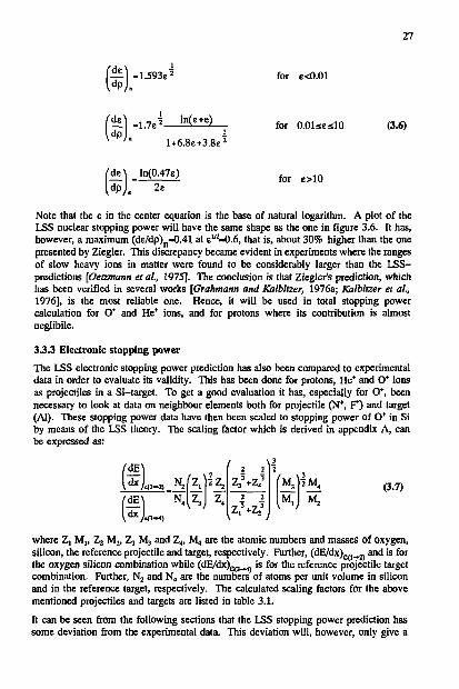
27
a •1.593e2 for e<0.01
(É1) . t .7 ,1 l n ( c + e ) for O.Ol^slO (3.6) (t (t
2 l+6.8e+3.8e2
ln(0,47e) 2e
for e>10
Note that the e in the center equation is the base of natural logarithm. A plot of the LSS nuclear stopping power will have the same shape as the one in figure 3.6. It has, however, a maximum (de/dp)n-0.41 at zm-4i.6, that is, about 30% higher than the one presented by Ziegler. This discrepancy became evident in experiments where the ranges of slow heavy ions in matter were found to be considerably larger than the LSS-predictions [Oetzmann et a!., 1975]. The conclusion is that Ziegler's prediction, which has been verified in several works [Grahmann and Kalbitzer, 1976a; Kalbitzer et at., 1976], is the most reliable one. Hence, it will be used in total stopping power calculation for O* and He* ions, and for protons where its contribution is almost neglibile.
3-3.3 Electronic stopping power The LSS electronic stopping power prediction has also been compared to experimental data in order to evaluate its validity. This has been done for protons, He* and O* ions as projectiles in a Si-target. To get a good evaluation it has, especially for O*, been necessary to look at data on neighbour elements both for projectile (N*, F*) and target (AT). These stopping power data have then been scaled to stopping power of 0* in Si by means of the LSS theory. The scaling factor which is derived in appendix A, can be expressed as:
w< N^jSz, f 2 A Z ^ Z , 3
N 4(Z,J Z, 2 2
z.-'+z/
^pH. (3.7)
where Z, M„ Zj M^ Zj M3 and Z4, Mt are the atomic numbers and masses of oxygen, silicon, the reference projectile and target, respectively. Further, (dE/dx)e(1_a and is for the oxygen silicon combination while (dE/dx)ep-i4^ is for the reference projectile target combination. Further, N2 and N4 are the numbers of atoms per unit volume in silicon and in the reference target, respectively. The calculated scaling factors for the above mentioned projectiles and targets are listed in table 3.1.
It can be seen from the following sections that the LSS stopping power prediction has some deviation from the experimental data. This deviation will, however, only give a

28
small error in the relative stopping power difference for neighbour projectile and target elements. This is true as long as the stopping power increases mono-tonically with the atomic number of the projectile and the target. It is, however, found from experiments that the electronic stopping power has an oscillating dependence upon the atomic number of the projectile, Z, [Omrod et al., 1965; Ward et al., 1979]. This Z, oscillation seems to be almost insensitive to the choice of target material, and it can be characterized as a weak oscillation around the Z, dependence predicted by the LSS theory. Experimental data indicate that
Reference Ion ! Target
Scaled to Ion ! Target
Scaling factor
0 ' Al 0 ' Si 0.8549
W Al 0* SI 0.8850
F" Al o- Si 0.8541
N" SI 0 ' Si 1.0369
P SI 0* Si 0.9976
He" Al He- Si 0.8426 |
Table 3.1 Scaling factors for some projectile (ion) - target combinations calculated from equation 3.7.
the electronic stopping power of N*, O* and F* ions in an Al target, are approximately equal [Grahmann and Kalbitier, 1976b]. This would give a maximum error of about 3.5% in the scaling factors listed in table 3.1.
6 3.100 > r*. 75
X TJ \ SO w
25
/ • NUCLEAR: -•;' • Ziegler [1977a]
ELECTRONIC: > Sirotinin et al. [1984] > Mertens and Krist [1982] > Santry and Werner [19811 • Grahmann and Kalbitzer T 1976a]
LSS, Lindhard et at. 11963b] Janni (Inol. Nuclear) [1982] Andersen and Ziegler [1977]
-0.50 M
> -0.30 <])
0.20 X X!
>%
to p
100 energy [keV]
Figure 3.7 Stopping power of protons in silicon. The nuclear contribution is ncglibile above 10 kcV. All data on electronic stopping power, except the LSS prediction, are experimental.
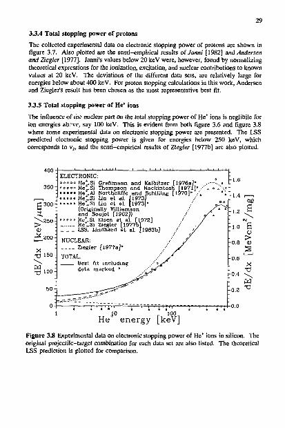
29
3.3.4 Total stopping power of protons
The collected experimental data on electronic stopping power of protons are shown in figure 3.7. Also plotted are the semi-empirical results ofJanni [1982] and Andersen and Ziegler [1977]. Janni's values below 20 kcV were, however, found by normalizing theoretical expressions for the ionization, excitation, and nuclear contributions to known values at 20 kcV. The deviations of the different data sets, are relatively large for energies below about 400 kcV. For proton stopping calculations in this work, Andersen and ZicgLer's result has been chosen as the most representative best fit.
3.3.5 Total stopping power of He* ions
The influence of the nuclear part on the total stopping power of He* ions is ncglibilc for ion energies abrve, say 100 keV. This is evident from both figure 3.6 and figure 3.8 where some experimental data on electronic stopping power are presented. The LSS predicted electronic stopping power is given for energies below 250 keV, which corresponds to v„ and the semi-empirical results of Ziegler [1977b] are also plotted.
400
350
C 300
~>-250 > r& ,2oo
x -a 150-
w -rj 100 :
ELECTRONIC: ooooo Het.Si Grahmann and Kalbitzer [1 aoDoaHe-.Si Thompson and Mackintosh
He„Al Northcliffe and Schilling [1 a . a a a He'-Si Lin et al. [19731 . . . . . He'.Si Lin et al. [1973]*
(Originally Williamson and Boujot [1962])
. . . . . He*.Si Eisen et at. [1972] He*, Si Ziegler [1977b] LSS, Lindhard et «1. [1963b]
NUCLEAR: Ziegler [1977a]*
TOTAL: Best fit including data marked *
976a]* [1971]* 970]* /
1.6
1.4
1.2
Q0
6 •l.o 6
V > •0.8 <U
0.6 X x)
0.4 \ Ed
no TJ
1° r 1 0 0 n He e n e r g y LkeV]
Figure 3.8 Experimental data on electronic stopping power of He* ions in silicon. The original projectile-target combination for each data set arc also listed. The theoretical LSS prediction is plotted for comparison.

30
Strange as it is, the experimental data on electronic stopping power seem to fall into two categories in the energy range from about 10 keV to just above 2 MeV. The upper best fit curve can be approximated with Ziegler's prediction, while the lower one is in good agreement with the result from the LSS theory and the extension of this. All the data sets, except from the solid squares, represent stopping of He* in Si. The solid square data points are scaled by help of the LSS theory from measurements of He* in Al. The separation disappears for energies above 2 MeV [Lin et al., 1973; Ziegler, 1977b], and the total stopping power of 5.47 MeV "'Am ct-particles can with good accuracy be set to 140 keV/u,m. This is not shown in figure 3.8.
3 J .6 Total stopping power of 0* ions
A collection of experimental data on electronic stopping power of oxygen ions in silicon are shown ii: figure 3.9. All these data are scaled data and the original projectile target combinations are listed. The best fit curve to these data is given as (dE/dx) c=27.177Eo; ! 1 5 9 (keV, urn units) in the energy range from 1 keV to 1 MeV. This is in the stopping power region III according to the definition in figure 3.5, the peak in the stopping power occurs at about 8 MeV [Northcliffe and Shilling, 1970]. The electronic stopping power predicted by the LSS theory is obviously too low compared to the experimental best fit curve. The deviation is about 19% at 200keV ion energy. Also shown in figure 3.9 is the total stopping power of O* projectiles in silicon.
6 a. > -id
900
800
700
600
500
400
300
200
100-
O-
(dE/dx). Best fit (dE/dxj„ Ziegler [1977a] (dE/dx)ror*L
ELECTRONIC: Al Northcliffe, Schilling [1970] Al Omrod et al. [1965 AI Omrod et al. 11365 'Al Omrod et al. [196S Si Tan et al. [1988] Al Ward et al. [1979] Al Schulz and Brandt [1982] Si Crahmann, Kalbitzer [1976a
Lindard et el. [1963b]
3.6
3.2 M
B 2.8 \
\ Id T3
20O_ 300 400 500
0 energy [keV] Figure 3.9 Stopping power of O* ions in silicon. The experimental data on electronic stopping power arc scaled from the listed projectile - target combination to O* in Si by the scaling factors listed in table 3.1.

31
3.3.7 Energy loss by nuclear collisions, v
The energy of an incident particle which is lost by nuclear collisions, v, will not be available for ionization. Consequently, it will not give any contribution to the output signal of the detector. Due to this, it will be very useful to know the dependence of v upon incident particle energy. Based on Ziegler's [1977a] semi-empirical formula, v is found numerically*' for protons, He* and O* ions. The results are plotted in figure 3.10, and it is clear that the reduction in the output signal of a silicon detector due to v, has to be taken into account in the low energy region. At higher energies, such as for 5.47 McV M 'Am ce-radiation, the influence of v is usually neglected. The fluctuation in v, E,,, is also of interest as it contributes to the "noise" or the total line-width of a detector. For 5.47 MeV ot-radiation, Lindhard et al. has calculated E„ t.. be about 4 keV FWHM [Lindhard et al, 1963a].
Figure 3.10 Calculated energy loss by nuclear collisions versus projectile energy for protons, He* and O* ions in silicon to the left, and relative to incident projectile energy to the right.
3.4 Channelling The stopping of charged particles in a crystalline target is more complex than in an amorphous or isotopic target. In the crystalline case most of the parameters related to the stopping, will be strongly dependent on the relative orientp.'ions of ion beam and target. This is because of the "channelling" effect which from a simple classical standpoint, can be understood as follows: If the direction of a charged particle incident upon the surface of a crystal lies close to a major crystal direction (i.e., close to a high symmetry axis), the particle will, with high probability, suffer a small-angle scattering as it passes through the first plane of atoms in the crystal. The probability is also high that this first deflection will be small enough so that the particle will suffer a similar
^ See appendix B for closer explanation.

32
small-angle scattering at the next atomic plane. Because of the ordered structure of the target, such a particle will undergo a correlated series of gentle small-angle collisions. Similar behavior occurs for incidence parallel to atomic planes. This results in a steering effect which causes such particles to follow trajectories which (for positively charged particles) oscillate in the open "channels" between atomic rows or planes.
3.4.1 Effects of channelling [Gibson, 19661
Channelled particles will have an anomalous energy loss. Several authors [Gemmell, 1974] have reported reductions in stopping power by factors up to 3 for major channelling directions. These particles will not suffer any elastic collisions with the crystal atoms so '.hat the nuclear stopping almost completely disappears [Grob et al, 1976; Eisen, 1968]. They will also encounter a lower average electron density per unit path length than particles having a random motion in the crystal. This causes a reduction in the electronic stopping power as well.
Channelled particles will also have an anomalous range as the range will increase correspondingly with the reduction of energy loss per unit length (stopping power). This has been verified experimentally by several authors [Piercy et al,, 19o3, Vos et at., 1988; Davies et al., 1964].
The beam divergence of an energetic particle beam which traverses an isotropic medium, will increase mainly because of multiple Coulomb scattering. Channelled particles, however, are only little deflected from the channel direction. This anomalous scattering will also cause a less broadening of an incident mono energetic peak at a given depth in the crystal.
Only one more effect of channelling will be mentioned here, and that is the anomalous radiation damage. It has been shown [Noggle and Oen, 1966] that the amount of radiation damage produced by high energy iodine ions in gold crystals is sharply reduced for incidence in channelling directions.
3.4.2 Condition for axial channelling
The main condition for channelling to occur along a crystal axis, is that the transverse energy of the ion is less than the energy barrier along the actual channel. The parallel channels along one crystal axis are potential wells separated from each other by this energy barrier. The barrier is set by the electron density and the interatomic spacing in the crystal. Based upon this model, Lindhard [1965; 1964] calculated a characteristic angle for axial channelling to be:
i i » . w . Ed
for V,s a
(3.8)
ip.ir/. Wpfi
[djl j for «P,>_
1 d

33
where ' l 1 is given in radians and d is the atomic spacing along the channel. An ion will be channelled if it is incident to a channel with an angle less than this characteristic angle. Note that equation 3.8 is given in cgs units. For conversion to keV units, see appendix A. A similar characteristic angle can be found for planar channelling [Gemmell, 1974].
3.4.3 Channelling in silicon
The silicon crystal has fee (face centered cubic) diamond structure with 8 atoms per unit cell. The lattice constant is a=5.431 Å, and the atomic spacing, d, along the channels are a, a/V2 and aV(3/4) for the <100>, <110> and <111> axes, respectively [Gemmell, 1974]. Lindhard's characteristic angle for channelling along the <111> axis in Si has been plotted against particle energy for protons, He* and O* ions in figure 3.11. The weak irregularities on the curves are due to the intermediate phases where %-a/d. An example of axial channelling is shown in figure 4.4 where a pulse height spectrum of 200 keV O* was recorded with a LEPD. Some of the ions are channelled through the LEPD dead layer some not, and the result is a double peak.
The transmission of 2.43 MeV protons incident along the <111> direction of a 60 um thick Ge crystal, is recorded in figure 3.12a [Gemmel, 1974]. The dark regions
5.0
a> 4.0 <0
2.0
0.0 10 10 '
Particle 10 3
energy [keV] Figure 3.11 Characteristic angle for channelling along the <111> axis in silicon for protons, He + and 0 + ions [Lindhard, 1964; 1965],
a)
<010:
b)
>-<001 >
Figure 3.12 a) <111> channelling of 2.43 MeV protons in Ge. Dark regions represent high particle intensity [Gemmel, 1974]. b) Stercographic <111> projection of Si [Appleton and Foti, 1977].

34
corresponds to regions of high particle^ intensity. The center of the star is the <111> axis, and the arms of the star are the {Oil}, {TlO} and {101} planes. The range of 2.43 MeV protons in amorphous Ge is approximately 43 (im. Ge and Si have the same type of crystal, and the pattern in this photograph can easily be recognized in the <111> stereographic projection of a Si crystal in figure 3.12b [Appleton and Foti, 1977].
3.S Stopping power of electrons For electrons it is customary to separate the total stopping power into two components: First, the collision stopping power, which is the average energy loss per unit pathlength due to inelastic Coulomb collisions with bound atomic electrons of the medium, resulting in ionization and excitation. This energy loss is absorbed in the medium rather close to the electron track. Second, the radiative stopping power which is the average energy loss per unit pathlength due to the emission of bremsstrahlung in the electric field of the nucleus and of the atomic electrons. Most of the energy lost here, travels far from the electron track before it get absorbed.
The election energy range of interest for the EDFMT is below 20 keV. It is, however, interesting to look at the LEPD's electron detection properties for somewhat higher energies also, say up to 100 keV. This is because the LEPD, in general, should be an excellent low energy electron detector. The total stopping power is dominated by the collision stopping power in this energy tange. The contribution of the radiative stopping power decreases with decreasing energy, and it is about 2% at 100 keV and less than 2%o at 50 keV [Pages et at., 1972; Berger and Seltzer, 1983]. Hence, only the collision stopping power will be considered in the following.
3.5.1 Collision stopping power
Based on Bethe's theory of slowing down, Rohrlich and Carlson [1954] have established a formula to calculate the electron collision stopping power [Pages et a!., 1972]:
/ d E \ 2nNAa<,m ec 2z i T2(T+2) + T*/8-(2T+l)ln2 2 _ . 1T2 /T.-112 " 2I 2 (T+l) 2
(3.9)
where N A is Avogadro's number, a<> the Bohr radius, m c the electron rest mass, c the speed of light, fj the ratio of the election speed to c, T the kinetic electron energy in units of nijC2, and 8 the density effect correction. Further, Z, A and I are the atomic number, atomic mass and the mean excitation energy of the medium traversed, respectively. The density-effect correction, 8, takes into account the reduction of the collision stopping power due to the polarization of the medium by relativistic charged particles. This effect is neglibile for the energy range of interest here [Siffert and Cache, 1968], so that 6 is neglected. The mean excitation energy, I, is set to be 173,1 eV for Si [Pages et at, 1972; Berger and Seltzer, 1983]. The resulting stopping power is plotted against energy in figure 3.13 (dashed line).
Based on the same theory, Nelms [1956] found a somewhat higher value of the collision stopping power. The difference is due to the uncertainty in the mean excitation energy, I, as a lower value (1=158 eV) has been chosen in Nelms1 work. The commonly

35
Ci
>
x -a \ Cd T3
accepted lower limit for the applicability of the above formula is 10 kcV. It has been shown that the lower the electron kinetic energy, the larger is the fraction of energy lost, on the average, in a single inelastic collision [Berger and Seltzer, 1983]. The calculation of the low-energy collision stopping power has been done by the statistical model, also called the free electron gas model [Ashley et ai, 1976; 1978]. Tung et al. [1976] have applied this theory for the several media, and the resulting stopping power for Si is plotted in figure 3.13. There are several examples of electron detection by silicon
implanted pn-diodes [Yamamoto ecai, 1984; 1989; Schmidt-Ott etai, 1989], but it has been impossible to find any experimental data on stopping power of electrons in silicon in this low energy region. The result of the free electron gas model has, however, been verified by several experiments with stopping of electrons in Al, Cu, Ag, and Au [Tung eta!., 1979].
In the energy region of interest, channelling will only have a weak influence on the stopping power of electrons in silicon. Electron diffraction processes will dominate for energies below 100 keV [Gemmell, 1974].
l i l l i l il
A III III! 1 ^ ^ El JfJ ,
m - ' /
B- —j-__L *~\\\\\ --• [HI / / TTI / lin / (III i. / V
1 "
/ •1 a- " T " " T T T I —HTT
z 4 a -.* A 'e'a' , z i 'o'a' .* 4 å'a
10 10 10 ;
energy [eV ft 1 0 '
Figure 3.13 Collision stopping power of electrons in Si. Dashed line: Plot of equation 3.9 [Pages et al, 1972]. Solid line: Statistical model prediction [Tung et ai, 1976].
3.6 Range It is convenient to define the range concept according to Lindard et at. [1963b]. The range, R, 's then length of the projectile's total path, sometimes also referred to as the effective range. The chord range, RQ also referred to as the vector range, is the distance from where the projectile enters the medium to where it stops. The projected range, RP, is the projection of RQ in a particular direction in the medium, that is, R P is the distance the projectile travels in this direction. Normally, this direction is perpendicular to the medium's surface, that is, R p equals the projectile's penetration depth. An illustration of these range concepts is given in figure 3.14.
The upper limit of a detector's dynamic range will be the particle energy where the projected range, RP, equals the thickness of the detector. It is also R P and the corresponding energy that are of interest when the energy loss in the dead layer of the
36
detector is to be determined. The projected range will to a good approximation be equal to the total path for energetic ions, while a deviation between these two will be found at lower energies. Generally, this deviation will increase with decreasing particle energy and mass, and therefore be largest for low energy electrons. Ziegler [1977b] has derived a semi-empirical expression of Rp as function of energy for He* ions, but in contrast to R, it is difficult to give an analytical expression of RP. An analytical expression of R where it is related to the stopping power, is, however, useful as the result represents the upper limit of RP.
3.6.1 CSDA range The range, R, can be calculated from the stopping power by the continuous-slowing-down approximation (CSDA). In this approximation energy-loss fluctuations are neglected, and the particles are assumed to loose energy continuously along their track, with a mean energy loss per unit pathlength given by their stopping power. The CSDA range is evaluated as:
R . j g p E (3-10)
and represents the average pathlength traveled by a particle as it slows down from an initial energy E<> to a final energy E,. This equals the lowest atomic ionization potential of the target, and can to a good approximation be set to E|=10 eV. For electrons, this formula has been applied to both the stopping powers in figure 3.13, and the results are shown in figure 3.15. The total path of protons, He* and O* ions are shown in figure 3.16. The calculations are based on data of (dE/dx)T shown in the figures 3.7-3.9, respectively. Concerning electronic stopping power, Andersen and Ziegler's [1977] prediction is chosen for protons. For He* ions, the lower curve in figure 3.8 is chosen as the best representation of the electronic stopping power. This choice is justified in section 4.3.3. A detailed explanation of the calculation method is given in appendix B.
The upper energy limit for the 280 um thick LEPD will be about 220keV for electrcns [Pages et ah, 1972; Berger and Seltzer, 1983; Nelms, 1956], about 6 MeV for protons [Andersen and Ziegler, 1977], and more than 20 MeV for He* ions [Ziegler, 1977b, extrapolated].
Figure 3.14 Illustration of the range concepts; total path (R), chord range (Re), and projected range (Rp).

e~ energy [eV] Figure 3.15 Total path, R, of electrons in silicon calculated by equation 3.10 and the stopping power data plotted in figure 3.13. The dashed line is valid for electron energies above 10 kcV.
Figure 3.16 Total path, R, of protons, He* and O* ions in silicon calculated by equation 3.10. Data on stopping powers arc taken from figures 3.7-3.9, respectively (concerning calculation method, sec appendix B).

38
Chapter 4
Detector surface dead layer and its influence on radiation detection -theory and experimental determination
The surface dead layer of the diode, also called the entrance window, can be defined as the detector medium the ionizing radiation has to penetrate without giving any contribution to the diode output signal. For a conventional ion implanted n-type particle diode this dead layer will be formed by a metal layer on the top, then a shallow SiO, layer, and the upper part of the ionunplanted p* layer. The S i0 2 layer is native oxide only, and can be neglected as it usually don't exceed some few nm. As the LEPD does not have any Al contact on top of the sensitive area, the dead layer consists of the upper part of the p* layer only.
4.1 Theoretical approach When a charged particle enters the diode surface interactions with the diode medium will start immediately. From there on the particle will continuously loose energy and generate electron hole pairs along its track. The electrons generated in the neutral p* region must diffuse to the depletion region before collection. The time for this diffusing process can be significant with respect to electron lifetime, and recombination may occur [Geist et ai, 1980]. The probability that a minority carrier generated at some location will be swept across the depletion zone before recombination, is called the collection efficiency, n. This is typically very close to unity in the depletion zone while it is usually reduced considerably in the vicinity of the front side of the diode. This is mainly due to surface recombination effects, but also Auger recombination is believed to play some role in p*n diodes [Geist et al., 1979]. This has been investigated for UV-enhanced photo diodes where the quantum efficiency is strongly dependent on the collection efficiency [Geist et ai, 1979; 1980; Geist, 1980; Wilkinson et ai, 1983]. An ordinary UV photo diode with antireflecting surface oxide may have values of T) as high as 82% at the surface.
The values of r| for charged particle detection will, however, be lower than those for UV-light detection. This is because the carrier density in the vicinity of the track of a charged particle will be much larger than the local carrier density caused by UV-light detection. This will affect the recombination rate and thereby decrease t| [Cache and
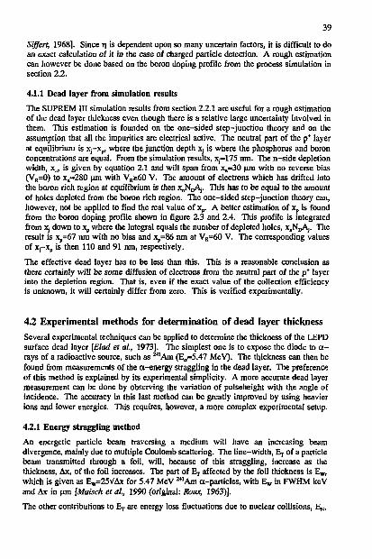
39
Siffert, 1968]. Since T| is dependent upon so many uncertain factors, it is difficult to do an exact calculation of it in the case of charged particle detection. A rough estimation can however be done based on the boron doping profile from the process simulation in section 2.2.
4.1.1 Dead layer from simulation results
The SUPREM III simulation results from section 2.2.1 are useful for a rough estimation of the dead layer thickness even though there is a relative large uncertainty involved in them. This estimation is founded on the one-sided step-junction theory and on the assumption that all the impurities are electrical active. The neutral part of the p* layer at equilibrium is Xj-xp, where the junction depth x, is where the phosphorus and boron concentrations are equal. From the simulation results, Xj-175 run. The n-side depletion width, x„ is given by equation 2.1 and will span from x„-30 urn with no reverse bias (VR=0) to x n-280 urn with VRa60 V. The amount of electrons which has drifted into the boron rich region at equilibrium is then xnN,jAj. This has to be equal to the amount of holes depleted from the boron rich region. The one-sided step-junction theory can, however, not be applied to find the real value of x p. A better estimation of x p is found from the boron doping profile shown in figure 2.3 and 2.4. This profile is integrated from Xj down to x p where the integral equals the number of depleted holes, x.NpAj. The result is xp=67 run with no bias and xp=86 nm at V„=60 V. The corresponding values of Xj-xp is then 110 and 91 nm, respectively.
The effective dead layer has to be less than this. This is a reasonable conclusion as there certainly will be some diffusion of electrons from the neutral part of the p* layer into the depletion region. That is, even if the exact value of the collection efficiency is unknown, it will certainly differ from zero. This is verified experimentally.
42 Experimental methods for determination of dead layer thickness Several experimental techniques can be applied to determine the thickness of the LEPD surface dead layer [Elad et al, 1973]. The simplest one is to expose the diode to ct-rays of a radioactive source, such as M 'Am (E„-5.47 MeV). The thickness can then be found from measurements of the a-energy straggling in the dead layer. The preference of this method is explained by its experimental simplicity. A more accurate dead layer measurement can be done by observing the variation of pulseheight with the angle of incidence. The accuracy in this last method can be greatly improved by using heavier ions and lower energies. This requires, however, a more complex experimental setup.
4.2.1 Energy straggling method
An energetic particle beam traversing a medium will have an increasing beam divergence, mainly due to multiple Coulomb scattering. The line-width, E,. of a particle beam transmitted through a foil, will, because of this straggling, increase as the thickness, Ax, of the foil increases. The part of Ej affected by the foil thickness is E^, which is given as Ew=25VAx for 5.47 MeV M A m a-particlcs, with E„ in FWHM keV and Ax in pm [Maisch et ai, 1990 (original: Roux, 1963)].
The other contributions to Bj are energy loss fluctuations due to nuclear collisions, E,,,

40
charge collection fluctuations, Ep, electronic noise, Ep, and source support broadening, E s . The square of the total line-width, Ej, will add up as the square sum of these contributions, since they are not correlated. This will be discussed more detailed in chapter 5, but as an example, Ep equals 3.6 keV for 5.47 MeV M 1 Am a-particles and a Fanofactor of 0.12. The contribution of the nuclear stopping term will be Fv-4 keV [Lindhard el at., 1963a]. The electronic line-width, Eg, which is dependent of the detector geometry and type, is about 2.5 keV for the 1 cm2, 280 um thick LEPD connected to a low noise preamplifier. The source line-width, Es, which is caused by straggling effects in the source support and in the source itself, is about 4 keV for a newly prepared source. It may, however, increase to several tens of keV after some time [Siffert et at., 1968 (original: Rebmeister, 1964)].
The total line-width, Ep, will for thin entrance windows (Ax~100 nm, Ew-7.9 keV) be dominated by Ej, and the uncertainty in Ep is also dominated by lack of knowledge about the accurate value of Ej. Most manufacturers do not specify an exact value of Es, they just guaranty it to be below some limit, often 20 keV. Further, note that E„ will vanish and E», will be reduced if the a-particles are channelled along a crystal axis. Also Ep may be weakly affected by channelling [Gibson, 1966]. The conclusion has to be that this is a simple method best suited for a rough determination of the entrance window thickness only.
4.2.2 Tilted beam method
This method is illustrated in figure 4.1. A particle beam with energy Ej incident perpendicular to the surface, will have a mean energy E after traversing the dead layer. The tilted beam will loose more energy, and have a lower corresponding mean energy, E'. The dead layer thickness can then be found from this difference '.:> energy loss as:
Ax— E-E ' dE dx
(cosqp-1) (4.1)
where <p is the tilt angle and (dE/dx) is the average stopping power. This is an accurate approximation as long as Ej, is large compared to E-E'. Otherwise the change in dE/dx with E has to be taken into account. Another approximation is done, too: The difference in nuclear absorption in the active volume at perpendicular and tilted incidence, v A - v i , which should be subtracted from E-E', is neglected. This is a good approximation in tilted beam measurements of thin dead layers with relatively high beam energies. If, on the other hand, Ax is measured directly from the difference between EQ and E in a well calibrated system, v taken into account even at high energies.
Figure 4.1 Schematic illustration of the beam method.
tilted
has to be
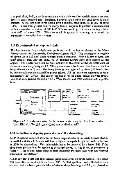
41
The peak shift, E-E', is easily measurable with a 5.47 MeV a-particle beam if the dead layer is some hundred nm. Problems, however, arise when the dead layer is much thinner. A 100 run dead layer would give a relative peak shift, (E-E')/E„, of about 0.1%. In this case, greater relative energy loss is required to perform a measurement with a reasonable precision. A 200 kcV O* beam would give a corresponding relative peak shift of about 10%. When so much is gained in accuracy, it is worth the experimental complication it causes.
43 Experimental set-up and data The ion beam surface analysis was performed with the ion accelerator at the Max-Planck-institut fur Aeronomie, Katlenburg-Lindau, FRG. This accelerator is capable of giving up to 320 keV single ionized positive particles. Four 4 kQcm n-type, 100 mm 2 circular area, 280 urn thick, <111> oriented LEPDs have been chosen as test objects. The diodes were, one by one, mounted in the center of the ion beam axis, as shown schematically in figure 4.2. Tilting was allowed for in one direction, and the ion beam diameter was 2 mm. The beam intensity was adjusted to about 500 ions/s, that is, low enough to prevent amplifier pileup effects. All the tests were performed at room temperature (23°-25°C). The energy calibration of the pulse-height analyzer (PHA) was done with gamma radiation from a I 3 3Ba source, and cross checked with a proton beam.
VACUUM CHAMBER
I " N Tenoelee
J&nn&ec TC953
J ^ Ortee * mod. 419
Nue.Data 7e* Nbisaa AOC
fannelec TC244 Shap. 4u»
OSCIU-O. SCOPE
Tectronbt mod. 475
Figure 42 Experimental setup for the mesurcments using the tilted beam method. The LEPD (UUT= Unit Under lest) can be tilted to ±50°.
4.3.1 Reduction in stopping power due to <111> channelling
All PHA spectra collected with the ion beam perpendicular to the diode surface, that is, in parallel with the <111> axis, will have a higher beam pulseheight due to the reduction in dE/dx by channelling. This pulseheight has to be corrected by a factor E/E c if the tilted beam method is to be applied as described above. E c and E are, as presented in figure 4.1, the beam's mean energies after traversing the dead layer with and without channelling, respectively.
A 200 kcV He* beam was first incident perpendicular to the diode surface. The diode was then tilted in steps up to maximum 50°. A PHA spectrum was collected at each position, and the beam pulse-heights relative to the pulse-height at 2.5°, are plotted in

42
J3 £ 1 . 0 0
3
figure 4.3. The diode was also tilted to the opposite side (negative angles) to assure correct symmetry. Lindhard's characteristic angle for channelling is, according to figure 3.11, in this case about 1.75°. Hence, the pulseheight at 2.5° should not be affected by channelling and can therefore be used as a reference corresponding to amorphous Si. Theoretical values for amorphous absorption in 50 nm and 75 nm thick dead layers are also plotted in the figure, and the effect of <111> channelling is clear. The factor E/Ec is in this case 0.983 and in good agreemenc with experimental results from Eisen et al. [1972].
The corresponding E/Ec factor for 200 keV O*, is 0.812. The characteristic angle for channelling in this case is about 2.75°. A PHA spectrum collected with (be diode tilted somewhat less than 2.75°, is shown in figure 4.4. Some of the ions in the beam have been channelled, some not, and E/Ec can be read directly from the spectrum when corrections for offset in the pulse-height analyzer is done.
43.2 Results
a
\ 'n^-» " N > : v \ : i \ "
10 20 30 40 50 60 Tilt angle tp [deg]
Figure 43 Relative pulse height of a 200 keV He* beam versus tilt angle. The circles represent measured values, the dotted and dashed curves theoretical values in isotropic dead layers of 50 and 75 nm thickness, respectively.
0 + 150
[keV] 100
energy Figure 4.4 200 keV O* pulse height spectrum collected with the LEPD tilted about 2.6°. Here E is about 146 keV and E r about 179 keV.
A computer program which corrects
All the data presented in figure 4.5 are found by the tilted beam method at 0° and 45°. The beam types and energies are listed together with the diode identifications. Corrections for <111> channelling at 0°, drift in amplification and PHA offset, have been done. A precision pulser is used to monitor the amplifier stability. dE/dx as the particle energy decreases, has been applied to find the dead layer thickness from the 0°-45° peak shift. A description of this program is given in appendix B. The diodes were also tilted to -45° to assure correct symmetry. As an example the E and E' peaks of 200keV He* beams are displayed simultaneously in figure 4.6. The dead layer thickness based on the data presented in figure 4.5, can be set to 64±5 nm at depletion. The uncertainty is set by the dispersion in repeated identical measurements. With an estimated over all uncertainty which also includes the measurement error in determining the 0°-45° peak shift, it is reasonable to conclude that the dead layer thickness is 64±8 nm (~15±2 ug/cm2) for depleted diodes in this batch. This is about 0.37xj. One simple test with an "'Am a-source and the tilted beam method has been done as a reference. This resulted in a dead layer thickness of 66±15 nm at

43
depletion. The uncertainty is set by the dispersion in repeated identical measurements, only.
ooooo Diode 50, 200keV 0* • • • • a Diode 51, 200keV 0*
Diode 51, 200keV He* Diode 51, 320keV He*
" < » • Diode 53, 200keV O* Diode 54, 200keV O* Diode 54, 200keV He*
Diode 50, best fit curve f Diode 51 , best fit curve
• 1 1 1 1 1 1 1
60 I I | I I I I I I I I I | I T T I I I"
80 100 Reverse bias [Volts]
19.8
: 1 8 . 8
17.8 g O
1 6 . 8 \
: 1 5 . 8 3 .
14.8 ><;
13.8
12.8
Figure 4.5 Results form the tilted beam method. The dead layer thickness is plotted against reverse bias for two of the diodes (50 and 51). The minima at about 8 V reverse bias will be commented in section 4.3.3.
43.3 Discussion
The results with He* beams are bdsed on the lowest stopping power curve in figure 3.8. This is done because this curve gives the best agreement with the measurements done with the O* beam. The upper one, Zicgler's curve, would result in an about 20 nm shallower dead layer. That is, if a reverse calculation, based on the dead layer thickness from the 0* measurements, were made, the He* measurements at 200 and 320 keV would then result in a dE/dx on the solid curve in figure 3.8. The conclusion would have to be that the semi-empirical results of Ziegler [1977b] are too high in this energy range.
Figure 4.6 200 keV He* pulse height spectra with the E (right) and E1 (left) peaks. The small pulser peak leftmost was used to monitor the amplifier stability.
The rapid decrease in the dead layer thickness at the first volts of biasing, is in good agreement with other measurements on ionimplantcd Si diodes [Grahmann and Kalbitzer, 1976b; Sebillotle el ai, 1970], The minima at about 8 V reverse bias, is most probably due to incomplete charge collection which has not been corrected for. The

44
energy calibration is done at V„=60 V and it is simply assumed that the collection efficiency, T|, is independent of the reverse bias. That is not true. The decrease in T] at the lowest biases has been confirmed in the case of proton generated charge in ion implanted diodes, by Grahmann and Kalbitzer [1976b]. The minima cannot be due to the weak dependence of the preamplifier amplification on the diode capacitance, since corrections are made for this effect. Neither can it be due to the shallow depletion layer at this voltage as the range of 200 keV He* and O* ions in Si are less than 2 urn. Even the intrinsic (no bias) depletion layer is deeper than this. An incomplete charge collection would cause lower values for E, E' and a smaller difference, E-E', between them (see figure 4.1). Hence, the calculated dead layer thickness will be lower than the actual value. The influence of this effect is largest at 0 V reverse bias and then decreasing with increasing bias voltage to about 20 V where it disappears. The actual dead layer thickness at low bias voltages is, due to this, deeper than the measured values presented in figure 4.5, the error being largest at 0 V reverse bias.
Finally, a comment should be made on the orientation of the tested diodes. It is clear that the <111> axis is perpendicular to the surface of the diode, but that do not make the orientation absolute. Nothing is known about the orientation in the two other surface plane dimensions. The stereographic <111> projection of the Si crystal in figure 3.12b illustrates this. Hence, in order to get an absolute orientation, the diode should have been rotated around the <111> axis with the ion beam incident at a given angle. Such an orientation tracking would take a lot of time, but then one could make sure that the {010}, {001}, {100}, {011}, {101} or {110} planes do not interfere with channelling at the 45° measurements.
4.4 Dependence of dead layer on fabrication process parameters It would of course be very interesting to inspect experimentally what influence changes in the fabrication process parameters have on Ax. Since this would be both costly and time consuming, some papers where this is done will be given as examples. All of them are dealing with boron implantation in silicon.
4.4.1 Examples
Sebillotte et al. [1970] have done experimental studies of the relationship between the dead layer thickness, Ax, and the bulk resistivity, the wafer orientation at implantation, the implantation dose, and finally the annealing temperature. Their diodes were made by implantation of 15 keV boron ions into n-type silicon. The 30 mm 2 active diode area was coated with a 10 nm thick gold film. Their devices had relatively large leakage current (-1 uA) at room temperature since the planar technology process was not yet developed. The thickness or C-V characteristics of the diodes are not given in their paper .so it is not possible to know the depletion voltage. Hence, it is not possible to compare the dependence of Ax on the reverse bias in their work, directly with the result for the LEPDs presented in figure 4.5. The rapid decrease in Ax at the first volts of biasing is, however, very consistent in both cases.
To find Ax they compared the pulse heights given by the diode when it was exposed to 100 keV protons and y-rays. The process parameters were altered one by one while the others were kept at the "standard" values. These are; 10" BVcm2 implantation dose,

45
1 kQcm n-bulk resistivity, implantation along the <111> axis, and 170°C annealing in 30 minutes under a dry argon atmosphere. To improve the energy resolution and accuracy of the measurements, they cooled the diodes down to 77 K. They did not find any changes in Ax with the operating temperature.
In the following Sebillotte's values of Ax at 100V reverse bias are given next to the parameters that were changed. The dead layer thickness increased when the implantation dose was increased: 10" BVcm2 (Ax-170 nm), 10 1 4 BVcm2 (Ax-285 nm), and 5-1014 BVcm2 (Ax-385 nm). An increase in Ax was also found with increasing n-bulk resistivity: 40 Qcm (Ax-130 nm), 150 Qcm (Ax-210 nm), 1 kQcm (Ax-295 nm), and 10 kQcm (Ax-400 nm). The dependence of Ax on crystal orientation at implantation were: <110> (Ax-420 nm), <111> (Ax-300 nm), and 8° to <111> (Ax-225 nm). The most interesting feature was the decrease observed in Ax when the annealing temperature was raised: 170°C 30 min dry argon (Ax-285 nm), 500°C 30 min vacuum (Ax-170 nm), and 700°C 15 min vacuum (Ax-130 nm).
Meyer [1969] has measured the dependence of Ax on the implantation energy at almost identical conditions. He used an implantation dose of 10° B7cm 2, 10 kQcm bulk resistivity and his diodes were annealed in 10 minutes steps of 100°C up to 600°C. The increase in Ax with implantation energy was very pronounced: 2 keV (Ax-35 nm), 4 keV (Ax-70 nm), 7 keV (Ax-110 nm), 10 keV (Ax-205 nm).
4.4.2 Conclusion
The tendency of the Ax dependence on implantation dose and energy plus bulk resistivity predicted by the SUPREM III simulation program in section 2.2, is verified by the experiments. There is, however, one important parameter not included in SUPREM III; the efficiency of the electrical activation as function of annealing temperature and time. All of the other parameters influence on Ax can be qualitatively understood from knowledge of the range of the implanted ions, reduction in this due to channelling, and also diffusion during the high temperature steps. Increased electrical yield is the only explanation to the pronounced decrease in Ax when the annealing temperature is raised. The planar process and efficient gettering processes allow for higher annealing temperatures without any degradation of the diode. Maisch et al. [1990] applied the planar process with implantation parameters 12.5 keV and 5 1 0 " BVcm2. They observed a pronounced fall in Ax (from about 140 to 60 nm) when the temperature was raised above 850°C. By process simulation they found the junction depth, Xj, to be about 170 nm. That is, Ax-0.35Xj, which is in good agreement with LEPD results. They also point out that annealing temperatures up to SKWC-lOfWC is necessary to produce an electrical yield of about 100%. This is in good agreement with the tendency of decreasing Ax with increasing annealing temperature referred to in the previous section.
The LEPD is annealed at temperatures where 100% electrical yield can be expected. Hence, if Ax is to be further reduced, this has to be done by altering some of the implantation parameters. One solution is to reduce the implantation energy at the same time as the implantation dose is increased to maintain a relatively low sheet resistivity in the emitter (p* layer). Even if the latter will increase Ax somewhat, the net result should be a reduction.

46
4.5 Influence of dead layer on radiation detection All the radiation types discussed in the previous chapter will be more or less affected by the LEPD dead layer. Detection of light is of no interest in this discussion as the photo diode is optimized for this mission. Hansen [1985] concludes that the photo sensitivity of the ame UV-enhanced photo diodes is mainly determined by the transmission coefficient at the diode surface antireflection layer.
4.5.1 Y- and X-rays
The attenuation of Y and x-rays in the energy range from 0.1 to 100 keV in the LEPD dead layer, is shown in figure 4.7. The attenuation is calculated as described in section 3.2. The solid line represents attenuation in the 64 nm thick dead layer, and the point of 50% attenuation is just below 300 eV. The dashed line includes attenuation in a 200 nm thick S i0 2 layer in addition to the dead layer. This is, in other words, the surface attenuation of a standard photo diode without any epoxy or equivalent surface coating. The presence of the anti-reflection oxide increases the attenuation a factor 2.6 in the energy range of 2 to 20 keV.
10
10 o
S 1 0 ' Tio-
10 '
10 "
1
2 ,"111111 a'
*. '
' s i'a'fl' 1 3 i 'aa' ' s * a e 0.1
E, I [kev]° 100
Figure 4.7 Relative attenuation of x-rays in: 64 nm Si (solid line) and 64 nm Si + 200 nm Si0 2 (dashed line). Attenuation data taken from Weigele [1973] and Storm and Israel [1967]. The dynamical energy range for x -
rays is then about 300 eV to 15 keV (figure 3.4) for the 280 urn thick LEPD concerning attenuation alone. The lower limit will due to noise be raised to about 5 keV for a LEPD and preamplifier operated in room temperature as described in chapter 5. Hence, the noise is the limiting factor even for a moderately cooled LEPD and preamplifier. Note, as mentioned in chapter 3.2.2, that the upper limit of 15 keV is raised towards 1 MeV in high flux applications.
4.5.2 Protons, He* and O* ions
The problem of calculating the projected range, Rp from knowledge of the total path of any particle, was mentioned in section 3.6. The same problem arises when the energy loss in the LEPD dead layer is to be calculated. The idealized results presented in figure 4.8 are based on the same stopping power data that are referred to in section 3.6.1. The particles are assumed to enter the LEPD perpendicular to the surface and then travel straight on throughout the dead layer without any deviation from this direction. The dead layer is assumed to be 64 nm. Hence, the plotted results represents the absolute minimum energy loss of the different particles. A flow chart of the program used for the calculations, is given in appendix B.

47
100
> caio
tt rf '11 s
III 0*- H<s* ' il
,' P | ,* IT
'il s s 3 4 « a B 4 • • 10 100 E0 of particles [keVJ
1000
1UU * =* s:in ][[
K ,. "* 0* o He* v a._
- a — -
tt P
1 7 « a 1 4 • • t 4 'a' 10 100 1000
E0 of particles [keV] Figure 4.8 Theoretical energy loss of protons, He* and O* ions in 64 nm Si to the left, and relative to incident particle energy to the right. The calculation method is explained in appendix B.
In practical applications with low energy particles it is not this energy loss alone that are of interest. After a particle has traversed the dead layer it will have an energy E=E,,-AE. A part of this energy, vA, will be lost to nuclear collisions as discussed in chapter 3.3.7. The effect of this is demonstrated in figure 4.9 where the sum of AE and v A has been measured for low energy protons and He* ions in two LEPDs. These measurements were performed at Swedish Institute of Space Physics, Kiruna, Sweden, with a General Ionex Corporation ion accelerator as ion source. The experimental set-up concerning electronics was identical to that shown in figure 4.2, except for the pulse height analyzer and the preamplifier which were a Maestro II and an Amptek A250, respectively. The beam energy was monitored with an electrometer, and a variable X-ray source with energies ranging from about 8 to 22 keV, was used for the spectrum calibration.
Some special LEPD's were used for this particular test. They are of the same type as those used for the dead layer measurements in section 4.3, except for their active area which is 33 mm 2 only. In figure 4.9 the dashed lines which are adopted from figure 4.8, represent the theoretical energy losses, AE, in a 64 nm amorphous dead layer. The solid lines represent the total theoretical reduction in
5 10 15 20 E 0 of p a r t i c l e s [ k e V ]
Figure 4.9 Energy losses in dead layer and by nuclear collisions versus particle energy. The markers represent experimental data for protons (solid) and He* ions (open). Lines are theoretical values in 64 nm silicon.

48
energy, AE+vA, where v A is found at Eø-AE according to figure 3.10. The measured values of AE+vA are consistently lower than the theoretical prediction for both protons and He* ions. This leads to the conclusion that the actual dead layer of the LEPDs in this batch is somewhat less than 64 nm which the theoretical calculations are based on. But the deviation may also be explained by channelling effects due to the <111> orientation of the diodes. The characteristic angle of axial channelling is large at these low energies, according to figure 3.11 *P=3.8° for protons and V=4.4° for He* ions, both at 10 keV. It is therefore likely that channelling will occur, recorded pulse height, that is the E/E c
no available publications dealing with the E/E c ratio in this experiment. The section of about 0=100 mm and it was fed through a 2 mm diameter collimator 2 cm above the LEPDs. In order to do measurements of the E/E c ratio, there would be a need for a more sophisticated collimator system in addition to a tilting arrangement. The preamplifier housing and LEPD collimator used in this experiment, are shown in figure 4.10.
This simple collimator system also made it difficult to do accurate measurements of the line width contribution from straggling in the dead layer, E».. The recorded spectra of 10, 12, 15 and 17 keV protons and 15 and 17 keV He* ions, are shown in figure 4.11. The total and electronic line-widths, Ej and B^ respectively, are listed for each spectrum. The total line width of the 17 kev He* ions for instance, E,=4.3 keV FWHM, will have a contribution of E ^ l keV FWHM from fluctuations in v [Lindhard et ah, 1963a], and Ee-2.8 keV FWHM from electronic noise, leaving behind about 3.1 keV FWHM. All this cannot be attributed to straggling, most of it has to be due to partly absorbed and scattered ions from the walls of the accelerator and the collimator.
4.5.3 Electrons
The energy loss in the 64 nm LEPD dead layer has in a similar manner been calculated for electrons. The result is plotted as solid lines in figure 4.12. The weak irregularities at E<y=10 keV are due to the two different data sets of stopping power above and below this energy as explained in section 3.5.1. Accurate measurements of the electron energy loss have also been performed, and these measured values are roughly 3 and 2.5 times larger than the theoretical ones at 10 and 20 keV incident electron energy, respectively. The experimental data are plotted as circles with a dashed best fit line in figure 4.12. The dashed line in the plot of the relative energy loss, AE/Eg, is based on these experimental data, too. Note that the calculated energy loss is based on the assumption the electrons total path, R, is equal to the dead layer thickness. This is not true since
Figure 4.10 The LEPD-preamplifier housing and collimator used for the measurements with low energy protons and He* ions.
but it is difficult to predict its influence on the ratio, at these low energies. There seems to be this specific subject, and was difficult measure beam available from the accelerator had a cross

49
V a a asisoo-
XI o
ln: 10 l«V p Et-3.1 keV JKHII H-2 e iuv nmu Peak at 0.10 l»V
g_1000-
Cou
nts
i i i 'Vb i'5'"""20
Detected energy [keV] Detected energy [keV]
c 3 o u
In: 15 kav p Et-3.0 k«V FWHU E,-2.6 k«V FVHU Puk «t 10.3 kaVj
tn: 1? k«V p
c Br-3.I k«V FVHU c tfZA k«V FVHU P**k at 11.D kaV
CO 600 -C / \ o f \ U f \
s.— « d 3 Z O 0 -
o o V J V
Detected energy [keV] Detected energy [keV]
Detected energy [keV] Detected energy [keV]
Figure 4.11 Pulse height spectra of 10,12,15, and 17 keV protons, and 15 and 17 keV He* ions collected with the 33 mm2 LEPD connected to an Amptck A250 preamplifier.
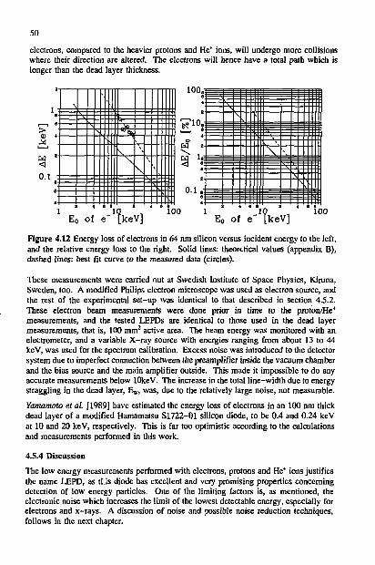
50
electrons, compared to the heavier protons and He* ions, will undergo more collisions where their direction are altered. The electrons will hence have a total path which is longer than the dead layer thickness.
100
>
w < o.i
1 - \ V rs— J
"s *» J ' T
| \ \ J \ \ \ « • — i E E É : 11 •. T
T a A 6 8 1 4 » a
K '10,
H 1«: <
0.1*
E 0 of e ^keV] 100
i — == V -
: = \ = g
• ~*n — „ \ \ *
|= = ^•J
^ 1 11 \', m
E 0 of e' ^keV] 100
Figure 4.12 Energy loss of electrons in 64 nm silicon versus incident energy to the left, and the relative energy loss to the right. Solid lines: theoretical values (appendix B), dashed lines: best fit curve to the measured data (circles).
These measurements were carried nut at Swedish Institute of Space Physics, Kiruna, Sweden, too. A modified Philips electron microscope was used as electron source, and the rest of the experimental set-up was identical to that described in section 4.5.2. These electron beam measurements were done prior in time to the proton/He* measurements, and the tested LEPDs are identical to those used in the dead layer measurements, that is, 100 mm 2 active area. The beam energy was monitored with an electrometer, and a variable X-ray source with energies ranging from about 13 to 44 keV, was used for the spectrum calibration. Excess noise was introduced to the detector system due to imperfect connection between the preamplifier inside the vacuum chamber and the bias source and the main amplifier outside. This made it impossible to do any accurate measurements below lOkeV. The increase in the total line-width due to energy straggling in the dead layer, E^, was, due to the relatively large noise, not measurable.
Yamamoto et al. [1989] have estimated the energy loss of electrons in an 100 nm thick dead layer of a modified Hamamatsu S1722-01 silicon diode, to be 0.4 and 0.24 keV at 10 and 20 keV, respectively. This is far too optimistic according to the calculations and measurements performed in this work.
4.5.4 Discussion
The low energy measurements performed with electrons, protons and He* ions justifies the name LEPD, as tlis diode has excellent and very promising properties concerning detection of low energy particles. One of the limiting factors is, as mentioned, the electronic noise which increases the Limit of the lowest detectable energy, especially for electrons and x-rays. A discussion of noise and possible noise reduction techniques, follows in the next chapter.
51
There is, however, one drawback with the LEPD presented here, namely its sensitivity to light. This may be a problem in detection of both particles and x-rays. Ambient light causes an additional flow of dc current through the diode, and this current acts as an increased leakage current which, as will be shown in chapter S, increases the noise. In LEPD applications where ambient light is a problem, one solution is to cover thi: LEPD with an opaque material such as a beryllium disk. This will, however, act as an increased dead layer which also increases the low energy limit. Another solution for charged particles, is to deflect them through a half-circle tube with diffuse, black baffles and then place the LEPD in the end of this tube. Such a detector could still cover a broad energy region if a variable electrostatic deflection arrangement is used. This will reduce the efficiency of the detector as it has to sweep through the energy region and at every moment be restricted to one specific energy for each type of particles.

52
Chapter 5
Noise in a silicon diode and a charge sensitive preamplifier -theory and practice
One of the most important properties of a detector used for radiation energy analysis, is good energy resolution or low noise. It is therefore of major interest to map the contributions from the different noise sources of a detector system in order to optimize the energy resolution. First it is necessary to take a closer look at the noise properties of the diode and the charge sensitive preamplifier, separately. The goal is to find a theoretical approach to the total noise which is measured in such a detector. The lowest detectable radiation energy in the silicon diode will be determined by this noise. In addition, the result is important for evaluation of the noise characteristics of a detector consisting of a diode in some combination with a scintillation crystal.
All contributions to the overall resolution of a detector system will be referred to as "noise" throughout this work. This may be statistical fluctuations in any detection or charge transport processes as well as electronic noise. The square of the total noise, Ef, of the detector shown in figure 5.1 may, as briefly mentioned in chapter 4.3.1, be expressed as the square sum of several uncorrelated noise sources:
EJ-EE+E£,+ES+E£+EF where E|-E£+EJJ (5.1)
where E , EQ and E A are electronic noise in the total detector system, the silicon diode and the charge sensitive preamplifier, respectively. The other, non-electronic noise sources, are: E* caused by energy straggling in the entrance window or deadlayer of the diode, Eg caused by energy straggling (or other fluctuations) in the radiation source, E„ due to fluctuations in nuclear stopping, and finally Ep which is associated with fluctuations in charge collection in the diode. It is possible to determine the influence of each one of these by measuring E,. at conditions where all the others are absent or neglibile. Noise due to energy straggling, E». and Eg, is easily eliminated just by using a y-radiation test source. To make sure that other effects, such as amplifier pileup and influence of back-scattered and secondary radiation, are eliminated, a precision pulser with a charge terminator can be used to measure Eg (and E,J when the energy calibration is known.

53
In the following, attention will be paid to intrinsic noise sources, only. This is noise which has its origin in the detector or amplifier system. Other external noise sources, which may cause problems, can be eliminated by use of proper shielding and grounding together with good filtering of the supply voltages. Nor is any attention paid to effects due to amplifier pile-up which may occur in high count rate applications. Such effects would cause baseline distortion and may be regarded as an extra noise source.
5.1 Experimental setup A "standard" detector configuration consisting of a silicon diode and a charge sensitive preamplifier with RC-feedback are chosen as test objects. The preamplifier is a hybrid Amptek A250 which represents the state-of-the-art concerning low noise and speed. One of the advantages of this preamplifier is the external FET which can be selected to match the impedance of the diode so that optimum noise properties is achieved. This is done by selecting a FET with input capacitance close to the diode capacitance. The effect of impedance matching would be lost due to the noise generated in the impedance matching components [Radeka, 1973]. Hence, a Sony 2SK152 FET with low input capacitance (0^=7.2 pF) was selected for this purpose. The drain current, I,,, was adjusted to 5.5 mA. Due to the low leakage current of the diode (!,<!. nA), a relatively high resistance was chosen for the biasing network, R ^ R ^ + R ^ ^ GQ.
The diode was ac-coupled to the preamplifier as shown in figure 5.1, and both were integrated as one unit in a well grounded bousing (Faraday box). All the components in the vicinity of the FET gate was mounted on teflon supports to minimize dielectric losses and parasitic capacitances. The pc-board and all the passive components were cleaned in an ultrasonic bath after mounting.
OUT
Figure 5.1 Schematic electronic diagram of the diode and the charge sensitive preamplifier. The hybrid Amptck A250 is a 14 pin dual-in-line package.

54
A Tennelcc TC244 shaping amplifier with unipolar and near Gaussian shaping was used for the noise measurements. The diode was biased from a Tennelec TC953 power supply, and an Ortec 419 precision pulser was used to generate the test pulses. All the pulseheight spectra wen- recorded on a Nucleus PCA8000 pulse-height analyzer which was integrated in an IBM PC AT.
The energy calibrations were done with two y-sources, one M l A m (59.5 keV) and one "Co (122 keV), and one X-ray source where M'Am-radiation cxitcs an Ag-foil (22.1 keV).
5.1.1 Cooling
Moderate cooling was achieved by use of a thermoelectric cooler. Two Peltron PKE36A001 peltier elements were coupled in series and connected to a driver network which also is used to set the desired temperature. A cross section of the detector housing is shown in figure 5.2. The hot side of the elements was water cooled to achieve optimal cooling efficiency. However, the circulating water cooling had to be closed during the measurements in order to prevent microphonics. It was also necessary to keep the peltier elements in a separate Faraday box to avoid noise transmission to the diode. The diode was mounted on top of an ISmm high alumina (A1203) cooling finger to minimize stray capacitances. The input FET of the preamplifier was mounted in a hole in this finger. This configuration allowed for cooling down to about -15°C.
Figure 5.2 Schematic cross section of the detector test chamber shown in figure 1.1. The upper section has a cover which is easily removable, and it is shielded from the noisy cooling clement by the copper disk which is grounded.
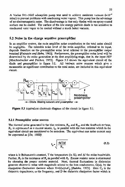
55 A Varian 941-5610 adsorption pump was used to achieve moderate vacuum (""10"2
mbar) to prevent problems with condensing water vapour. This pump has the advantage of no electromagnetic noise. The disadvantage is that only diodes with an epoxy coated surface can be cooled. The surface of the low energy particle diode is too sensitive to condensed vater vapor to be cooled without a much better vacuum.
5.2 Noise in the charge sensitive preamplifier In an amplifier system, the main amplifier noise contribution to the total noise should be negligible. The tolerable noise level of the main amplifier, referred to its input, depends therefore on the preamplifier noise level referred to the preamplifier output terminal [Fairstein and Hahn, 1965]. Furthermore, the preamplifier noise level will be determined by the noise generation at the first amplifying stage, that is, the input FET [Motchenbacher and Fitchen, 1973]. Figure 5.3 shows the equivalent circuit of the diode and preamplifier in figure 5.1. All intrinsic noise sources which give a measurable or significant contribution to the total noise, arc included in this equivalent circuit.
Rsd
lin ] Ish C;
RsF
-$>t^-R.U,
VsT" M
Noiseless ± preamplifier
-*— Diode' Biasing network and preamplifier —»-
Figure 5 3 Equivalent electronic diagram of the circuit in figure 5.1.
5.2.1 Preamplifier noise sources
The thermal noise generated in the bias resistors, Rj, and R„,, and the feedback reislor, Rp is represented as a current source, IR, in parallel with the two resistors which in the equivalent circuit arc considered to be noiseless. The equivalent rms noise current may be expressed as [Ott, 1988]:
N
4kTAf (5.2)
where k is Boltzmann's constant, T the temperature (in K), and Af the noise bandwidth. Further, R T is (he resistance of R,, in parallel with R,. Excess resistor noise is eliminated by choosing the proper resistor material. Next, thermal fluctuations in dielectrics generate electronic noise with magnitude related to the Loss conductance, G((o), by the dissipation-fluctuation theorem where D=G(o))/a)Cd [Radeka, 1973]. Here Ct is the dielectric capacitance, o the frequency, and D the dielectric dissipation factor which is

56 assumed to be constant for materials with relatively low losses [Radeka, 1973; 1968]. Such dielectric losses will more or less be present in the encapsulating material of the FET and in other materials in the vicinity of the terminals from the diode output to the FET gate. Note that the dielectric material does not have to be in contact with these terminals in order to feed noise into them. In figure 5.3 this noise source is represented by the noise current source IG, and may be expressed as [Radeka, 1968]:
IG-y/&tkTDC„fAf ( 5 - 3 )
The intrinsic noise in the FET is the thermal noise of the conducting channel modified by the effect of channel width modulation. The equivalent rms noise voltage is then [Radeka, 1973]:
V i F-/4kTR^Af where R ^ j g . (5.4)
where R,F is the equivalent channel resistance and g„ the transconductance of the FET Finally, there will be some flicker (or 1/f) noise in the FET. This results in the following rms noise voltage:
V ' N ±U **
where A, is a constant defined by the relation between the spectral density and the rms noise voltage of the flicker noise. For a typical FET A^IO" 1 4 V 2.
5.2.2 Preamplifier noise relative to main amplifier output
The total preamplifier noise, E A , is found by integrating the above noise sources by the total input capacitance, C& over the bandwidth of interest. The total noise will then be [Llacer, 1975; [Goulding, 1977]:
N BI(N, 2)^ k T D C ,'<N: i>2kTR a ,C;<N a
2)H.^Sl(N 2„> <s-«) Rj. jt 2
where k c~5.2910 1 6 is a conversion factor from ENC1 0 to keV FWHM relative to silicon. The four terms represent the integrals of equations 5.2 to 5.5 respectively, and they are expressed in (ENQ 2 . The values of the noise constants <Nj> are listed as function of n for RC-CR" shaping networks in table 5.1. The step noise constant, <N2>, is proportional to the peaking time, x^ while the delta noise constant, <N 2>, is proportional to the inverse of i 0 . The other noise constants, <N 2
U > and <N 2
] t>, are
" ENC (Equivalent Moise Charge) is the charge which in a slep function at Ihc input of a noise-free preamplifier, gives an output signal whose magnitude equals the rms noise at Ihc output of a real preamplifier.
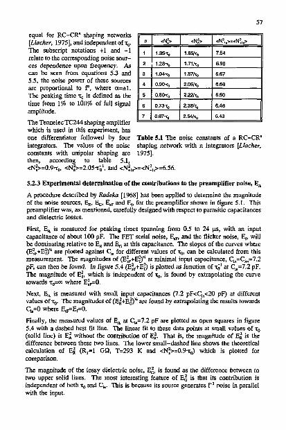
57
equal for RC-CR" shaping networks [Llacher, 1975], and independent of T0. The subscript notations +1 and -1 relate to the corresponding noise sources dependence upon frequency. As can be seen from equations 5.3 and 5.5, the noise power of these sources are proportional to f", where ot=±l. The peaking time x 0 is defined as the time from 1% to 100% of full signal amplitude.
The TennelecTC244 shaping amplifier which is used in this experiment, has one differentiator followed by four integrators. The values of the noise constants with unipolar shaping are then, according to table 5.1, <Nl>=0.9-z„, < N ? > = 2 . 0 5 T - 0
1 , and <Nf,
n <Nf> <Nf> < N ? „ > = < N : „ >
1 1.85-t, 1.85/to 7.54
2 1.28-r, 1.71/x, 6.90
3 1.04-tj 1.87/tj, 6.67
4 0.90-x„ 2.05/n, 6.56
S 0.8OT„ 222/x, 6.50
6 0.73T„ 2.38/T, 6.46
7 0.67^ 2.54/i„ 6.43
Table 5.1 The noise constants of a RC-CR" shaping network with n integrators [Llacher, 1975].
,>=<N?„>=6.56.
5.2.3 Experimental determination of the contributions to the preamplifier noise, E A
A procedure described by Radeka [1968] has been applied to detennine the magnitude of the noise sources, Ej, EG, E l F and E„ for the preamplifier shown in figure 5.1. This preamplifier was, as mentioned, carefully designed with respect to parasitic capacitances and dielectric losses.
First, E A is measured for peaking times spanning from 0.5 to 24 us, with an input capacitance of about 100 pF. The FET serial noise, E,F, and the flicker noise, E„ will be dominating relative to Eg and E G at this capacitance. The slopes of the curves where (E;F+Ef)K are plotted against C^ for different values of T 0 , can be calculated from this measurement. The magnitudes of (E^F+Ej)4 at minimal input capacitance, C,n=C1„=7.2 pF, can then be found. In figure 5.4 (E*F+E;) is plotted as function of TJ 1 at Q,=7.2 pF. The magnitude of E , which is independent of T0, is found by extrapolating the curve towards T0=°° where E^=0.
Next, E A is measured with small input capacitances (7.2 pF<C in<20 pF) at different values OIXQ. The magnitudes of (Ej+Ej)'4 are found by extrapolating the results towards C t a=0 where E jF=E,=0.
Finally, the measured values of E A at C„=7.2 pF are plotted as open squares in figure 5.4 with a dashed best fit line. The linear fit to these data points at small values of x„ (solid line) is E A without the contribution of Ej. That is, the magnitude of E | is the difference between these two lines. The lower small-dashed line shows the theoretical calculation of E | (R^=l Gfi, T=293 K and <Nj>=0.9-to) which is plotted for comparison.
The magnitude of the lossy dielectric noise, Ej, is found as the difference between to two upper solid lines. The most interesting feature of Eg is that its contribution is independent of both T0 and Q,. This is because its source generates f"1 noise in parallel with the input.
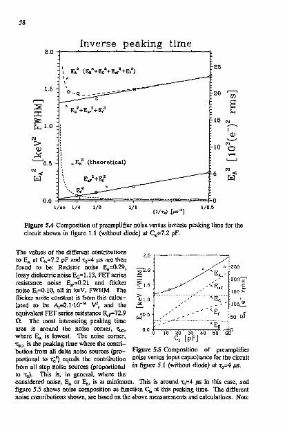
58
2.0 Inverse peaking time
l /oo 1/4 1/2
Figure 5.4 Composition of preamplifier noise versus inverse peaking time for the circuit shown in figure 1.1 (without diode) at C t a=7.2 pF.
The values of the different contributions to E A at C„=7.2 pF and T 0 = 4 us are then found to be: Resistor noise ER=0.29, lossy dielectric noise EG=1.13, FET series resistance noise E l F=0.21 and flicker noise E,=0.10, all in keV, FWHM. The flicker noise constant is from this calculated to be /V-2.110-" V 2, and the equivalent FET series resistance R jF»72,9 Q. The most interesting peaking time area is around the noise comer, Trø where E A is lowest. The noise corner, Trø is the peaking time where the contribution from all delta noise sources (proportional to T; 1 ) equals the contribution from all step noise sources (proportional to to). This is, in general, where the
considered noise, E A or E & is at minimum. This is around T0=4 US in this case, and figure 5.5 shows noise composition as function C t a at this peaking time. The different noise contributions shown, arc based on the above measurements and calculations. Note
Figure 5.5 Composition of preamplifier noise versus input capacitance for the circuit in figure 5.1 (without diode) at t 0 =4 lis.
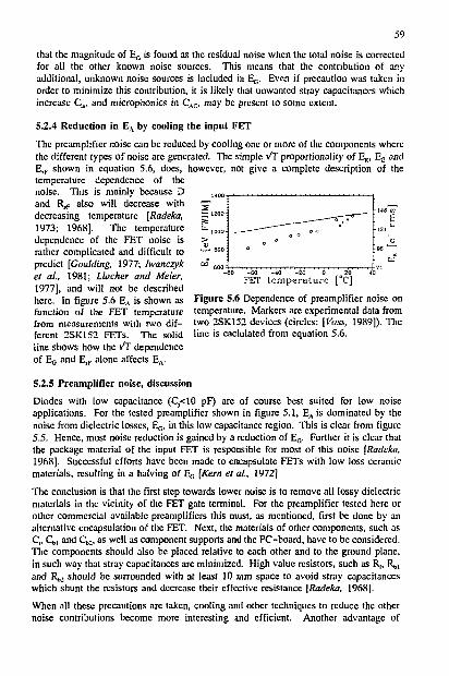
59
that the magnitude of E 0 is found as the residual noise when the total noise is corrected for all the other known noise sources. This means that the contribution of any additional, unknown noise sources is included in E 0 . E r a if precaution was taken in order to minimize this contribution, it is likely that unwanted stray capacitances which increase Cm, and microphonics in C A C , may be present to some extent.
5.2.4 Reduction in E A by cooling the input FET
The preamplifier noise can be reduced by cooling one or more of the components where the different types of noise arc generated. The simple vT proportionality of E„, E G and E l F shown in equation 5.6, docs, however, not give a complete description of the temperature dependence of the noise. This is mainly because D and R j F also will decrease with decreasing temperature [Radeka, 1973; 1968]. The temperature dependence of the FET noise is rather complicated and difficult to predict [Goulding, 1977; Iwanczyk et ai, 1981; Llocher and Meier, 1977], and will not be described here. In figure 5.6 E A is shown as function of the FET temperature from measurements with two different 2SK152 FETs. The solid line shows how the vT dependence of E 0 and E,F alone affects EA.
US Ul
B
FET tempera ture [°C]
Figure S.6 Dependence of preamplifier noise on temperature. Markers are experimental data from two 2SK152 devices (circles: [Voss, 1989]). The line is caclulatcd from equation 5.6.
5.2.5 Preamplifier noise, discussion
Diodes with low capacitance (C^IO pF) arc of course best suited for low noise applications. For the tested preamplifier shown in figure 5.1, E A is dominated by the noise from dielectric losses, E c , in this low capacitance region. This is clear from figure 5.5. Hence, most noise reduction is gained by a reduction of E 0 . Further it is clear that the package material of the input FET is responsible for most of this noise [Radeka, 1968]. Successful efforts have been made to encapsulate FETs with low loss ceramic materials, resulting in a halving of E G [Kern et at., 1972]
The conclusion is that the first step towards lower noise is to remove all lossy dielectric materials in the vicinity of the FET gate terminal. For the preamplifier tested here or other commercial available preamplifiers this must, as mentioned, first be done by an alternative encapsulation of the FET. Next, the materials of other components, such as C„ Q , and Q,2, as well as component supports and the PC-board, have to be considered. The components should also be placed relative to each other and to the ground plane, in such way that stray capacitances arc minimized. High value resistors, such as R,, R b l
and R ; should be surrounded with at least 10 mm space to avoid stray capacitances which shunt the resistors and decrease their effective resistance [Radeka, 1968].
When all these precautions arc taken, cooling and other techniques to reduce the other noise contributions become more interesting and efficient. Another advantage of
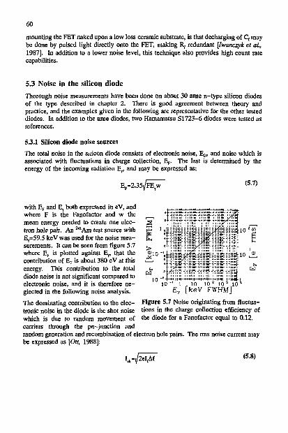
60
mounting the FET naked upon a low loss ceramic substrate, is that decharging of C, may be done by pulsed light directly onto the FET, making R; redundant [Iwanczyk et al., 1987]. In addition to a lower noise level, this technique also provides high count rate capabilities.
53 Noise in the silicon diode Thorough noise measurements have been done on about 30 ame n-type silicon diodes of the type described in chapter 2. There is good agreement between theory and practice, and the examples given in the following are representative for the other tested diodes. In addition to the ame diodes, two Hamamatsu S1723-6 diodes were tested as references.
53.1 Silicon diode noise sources
The total noise in the silicon diode consists of electronic noise. En, and noise which is associated with fluctuations in charge collection, Ep. The last is determined by the energy of the incoming radiation E,, and may be expressed as:
E p - Z ^ F E j W ( 5 > 7 )
with Ep and E, both expressed in eV, and where F is the Fanofactor and w the mean energy needed to create one electron hole pair. An MAm test source with £,=59.5 keV was used for the noise measurements. It can be seen from figure 5.7 where Ep is plotted against E,, that the contribution of E ; is about 380 eV at this energy. This contribution to the total diode noise is not significant compared to electronic noise, and it is therefore neglected in the following noise analysis.
The dominating contribution to the electronic noise in the diode is the shot noise which is due to random movement of carriers through the pn-junction and random generation and recombination of electron hole pairs. The rms noise current may be expressed as [Ott, 1988]:
nm 11 mini i mini -10 - 1 10 10 2 10 * 10
E 7 [keV FWHM] Figure 5.7 Noise originating from fluctuations in the charge collection efficiency of the diode for a Fanofactor equal to 0.12.
\rfi*& (5.8)
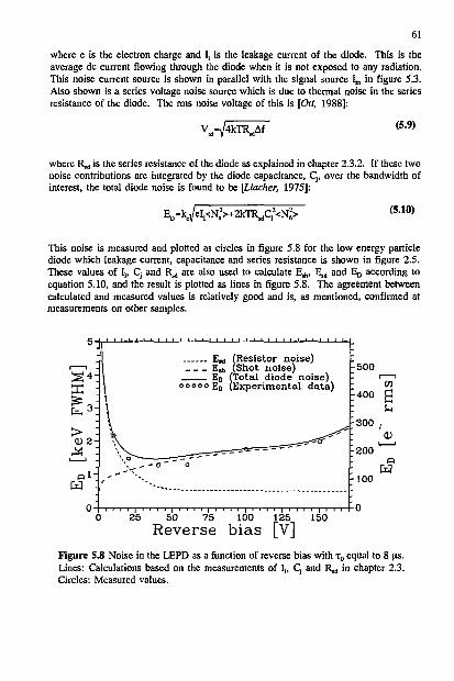
61
where e is the electron charge and I, is the leakage current of the diode. This is the average dc current flowing through the diode when it is not exposed to any radiation. This noise current source is shown in parallel with the signal source I,n in figure 5.3. Also shown is a series voltage noise source which is due to thermal noise in the series resistance of the diode. The rms noise voltage of this is [Ott, 1988]:
v W 4 k T M f (5.9)
where R , is the series resistance of the diode as explained in chapter 2.3.2. If these two noise contributions are integrated by the diode capacitance, C,-, over the bandwidth of interest, the total diode noise is found to be [Llacher, 1975]:
VW eVN>+2kTR r fCf<N 4
2> (5.10)
This noise is measured and plotted as circles in figure 5.8 for the low energy particle diode which leakage current, capacitance and series resistance is shown in figure 2.5. These values of I,, C, and R r i are also used to calculate E J h, E l d and EQ according to equation 5.10, and the result is plotted as lines in figure 5.8. The agreement between calculated and measured values is relatively good and is, as mentioned, confirmed at measurements on other samples.
s 4 i
> <L> 2
E«i (Resistor noise) E,h (Shot noise) ED (Total diode noise)
OOOOOED (Experimental da ta )
i i i i '
25
-500 m
; 400 g U
300 , <D
•200 ' '
-100
a
50 75 100 125 Reverse bias [V]
150
Figure 5.8 Noise in the LEPD as a function of reverse bias with x0 equal to 8 us. Lines: Calculations based on the measurements of I„ C; and R l d in chapter 2.3. Circles: Measured values.
62 5.3.2 Reduction in diode noise by cooling the diode
An epoxy coated ordinary photo diode (AE9873) with relatively large leakage current was chosen for the cooling test. This diode is 280 um thick with 100 mm 2 active area, and the bulk resistivity is about 6 k£2cm. The epoxy coating was necessary for optimal protection of the diode surface in the moderate vacuum. Otherwise, condensing vapor would cause an unwanted increase in the surface leakage current. The leakage cuwent of this diode is shown as function of reverse bias and temperature in figure 5.9. It was necessary to have a diode with relative large leakage current at room temperature. Otherwise the preamplifier noise would be totally dominating for noise measurements at lower temperatures. The leakage current of this device increases a factor 2.7 for every 10°C temperature increase for biasing voltages from 0 V to -35 V (depletion voltage). This is very consistent with theoretical predictions [Herbst, 1970]. The increase in I, with T is lower for biasing voltages above the depletion voltage. At -50 V biasing voltage I, increases only a factor 1.8 for every 10°C increase in T.
0 5 10 15 20 25 30 35 40 4 5 50 Reverse Bias [V]
Figure 5.9 Measured leakage current in an epoxy coated photo diode (100 mm2, 280 urn, 1.5-3 kficm) plotted against temperature and reverse bias.
The solid line in Figure 5.10 is the total diode noise, E„, as function of temperature calculated from measured leakage current which is shown in figure 5.9. The decrease in the thermal resistor noise, E I d, is also taken into account in this calculation even if it is overwhelmed by the much more pronounced decrease in E s h. The circles in figure 5.10 are measured noise values, and their discrepancy from the theoretical prediction at the highest temperatures may be explained by the high relative uncertainty in I, at this
63
temperatures. Figure 5.11 shows a photograph of the applied cooling arrangement inside the chamber shown in figure 5.2.
The good agreement between the measured values of E„ and those calculated from the measurements of [„ Cj and RM is confirmed from measurements on other diodes [Johansen et al., 1988]. It is therefore possible to predict E B with good accuracy from measurements of I, and Cj (R^ can be calculated from measurements of Cj).
S X m- 500 E
Diode t e m p e r a t u r e [°C]
Figure 5.10 Dependence of total noise in a depleted LEPD upon temperature. The line is calculated due to equation 5.10, and the circles represents measured noise.
Figure 5.11 The cooling arrangement inside the test chamber (figure 5.2). The FET is placed inside a hole in the cooling finger and the diode is placed on the top. Heat conducting pasta is used between the cooling finger and the UUTs.
5.3.3 Ballistic deficit
Ballistic deficit is attenuation and delay of the diode signal caused by the scries resistance of the surface layer of the detector. This is the p* layer in the case of the LEPD. This will act as an extra noise source as the signal attenuation increases towards the center of the diode surface. To check for such signal attenuation in the center region of the active area, the LEPD has been tested with a 5.47 MeV " A m ct-source. The radiation was fed through a hole (0=1 mm) at several positions from the center towards the edge-contact, and a pulse-height spectrum was recorded in each position. The gain stability of the amplifier was monitored with a precision pulser, but there was not found any change in the pulsehcight. This is in good agreement with theoretical predictions

64
[Rawlings and Deighton, 1989], and the conclusion is that ballistic deficit does not represents any problem for the LEPD.
5.4 Total noise The total noise of the low energy particle diode and the preamplifier described above is shown in figure 5.12. The noise comer, that is the peaking time at which minimal total noise is achieved, is about 8us. This can be seen from figure 5.13 where the total noise of the LEPD and the Amptek A250 preamplifier is plotted against reverse bias for several peaking times. The total noise could be reduced in many ways, but it is clear that it is the preamplifier noise, EA, which is dominant in this test, diode capacitance is, however,
5 -
f °oooo Er (Total no(se) \ E» (Preamplifier noise) \ ED (Diode noise)
i • f l ;
i • f l ;
1
50 75
Reverse 100
bias [V] Figure 5.12 Total, diode and preamplifier noise for the LEPD and the Amptek A250 measured at T„=4 (is. The lines are best fits to the measured data.
The relative
large here; 280 urn thickness and 100 mm2 active area gives Cf 45 pF at depletion. A 500 um thick diode with 25 mm2
active area would have C—7 pF. The preamplifier noise would then, as can be seen from figure 5.5, be reduced to about 1.25 keV FWHM when the diode is depleted. On the other hand the active volume of the diode is more the halved, and it is reasonable to expect a decrease in the diode noise, as well. Thus, the most pronounced noise reduction will still be gained by a further reduction of the preamplifier noise as suggested in section 5.2.5. ihe same conclusion is drawn when the charge sensitive preamplifier is used with other low noise semiconductor diodes such as Hgl2 [Iwanczyk, 1989]. Cooling of the diode and the input FET does not alter this picture as the noise of the diode has the largest temperature dependence.
Figure 5.13 Total noise of the LEPD and Amptek A250 preamplifier against reverse bias and peaking time. Markers are measured data and the lines best fit curves.

65
Chapter 6
Silicon diode readout of scintillation light
Altogether it can be concluded that the diodes treated in this work are very well suited as detectors for both low energy particles and x-rays. The practical low energy limit is at present time set by the preamplifier noise. Concerning detection of low flux x -rays, the high energy limit is about 15 keV because of the relatively low attenuation cross section of the diode. It has turned out to be difficult to make low noise silicon diodes thicker than about 1 mm. The gettering processes by which the low leakage current is accomplished, are not efficient above this thickness. Even lithium compensated p-type silicon Si(Li) diodes which can be made somewhat thicker, will suffer from low detection efficiency compared to other high Z materials.
The stopping efficiency is greatly enhanced and the upper energy limit is raised to several hundreds cf keV when a scintillation crystal is used as radiation stopping material. Here the stopping efficiency is determined by the scintillation crystal shape, size and type. Normally a conventional photo multiplier tube (PMT) is used as readout device for the scintillation light. The aim is, however, to realize another, more compact detector which also is more suitable in a position sensitive configuration. A method which has been used in many high energy physics applications, is to use a silicon diode as readout device of the scintillation light. In the following most attention will be paid to how this configuration affects the energy resolution of the detector. To avoid confusion it is very convenient to denote the scintillation crystal as SC, the photo diode as PD, and the photo multiplier tube as PMT. These abbreviations will also be used as subscripts so that FWHMS C, for instance, is the line-width based on to the energy deposited in the scintillation crystal.
6.1 Photo diode readout of scintillation light The ame UV-enhanced photo diode is well suited as readout device for scintillation light. This is due to its high quantum efficiency, Q c , which for the epoxy coated diode is approximately 80% over a broad wavciength range spanning from about 320 to 920 nm (sec figure 3.1). This incorporates the emission spectra of most scintillation crystals, even the CsI(Tl) crystal which, in spite of its excellent properties, has been little used due to the spectral mismatch to most PMT photo cathodes.
66
6.1.1 Appropriate scintillation crystals
Some properties of the most interesting inorganic scintillation crystals are listed in table 6.1. Note that all quantities given in % in this work are supposed to be converted to their absolute values when they are referred to in equations and calculations. Concerning spectral matching, the ame UV-enhanced photo diode can be used as readout device for all these, so no attention has to be paid to this when choosing an appropriate crystal. The scintillation light decay constant, however, has to be considered with respect to count rate and noise performance. High count rate applications require a short amplifier peaking time, T0, while low noise is achieved with x 0 close to the noise comer. Optimal readout of the scintillation light is, on the other hand, carried out with XQ several times larger than the decay constant of the crystal. This is necessary to make sure that integration is done over the whole scintillation pulse. The fastest decaying crystal listed in table 6.1 is the relatively new GSO crystal. Faster decaying scintillators are available if reductions in stopping efficiency (Plastic scintillators) or scintillation efficiency (CsF) can be accepted.
Crystal: Chemical:
NaI(Tl) CsI(Tl) BGO B^GejOu
cwo CdWO,
GSO CeÆdjSiOj
Wavelength at maximum emission, A^^ [nm] 415 550 480 540 430
Decay constant [ns] 230 1000 300 5000 60
Scintillation efficiency at 20°C, O c [%]
11.3" 11.9" 2.1" 3.8" 3.6"
Afterglow (after 3ms) [%] 0.3-5 0.5-5 0.1 0.1 -Refractive index at X,,^ 1.85 1.80 2.15 2.3 1.9
Density [g/cm3] 3.67 4.51 7.13 7.90 6.71
Relative attenuation, I/Io [%] ISOkeV in 10mm crystal at: 511keV
89.14 28.82
98.64 41.73
100.00 61.52
99.95 57.51
99.54 49.03
Hygroscopic? Yes Slightly No No No
Table 6.1 Some important properties of commonly used inorganic scintillation crystals. References: •) [Holt et at., 1988] **) Hitachi data-sheet.
The scintillation efficiency, O c . is defined as the fraction of energy emitted as scintillation light to the total energy deposited in the crystal by a y-quantum or equivalent. The relatively low values of Q c is the major drawback with the scintillation crystal -photo diode combination. A large portion of the incoming radiation energy is lost and the lowest detectable energy level is therefore raised correspondingly. Hence, Q c is the most important parameter in low energy applications. The refractive indices of the crystals is maybe of minor importance, but good matching of the refractive indices of the crystal, diode surface (SiO,) and any optical coupling compounds in between, is of course an advantage in order to optimize the transmission. The scintillation efficiency is normally quoted as the relative light yield compared to a NaftTl) crystal on a PMT
67
with a S - l l photo cathode. The Q c-values of listed in table 6.1 is, however, absolute values measured by Holl et al. [1988]. They have used small test crystals shaped as truncated pyramids and photo diodes with somewhat larger active areas to optimize the light collection. Their values are furthermore corrected for any spectral mismatch, light loss due to imperfect surface reflection, decay time - shaping time errors, and temperature differences. These Q c values are found from measurements on many samples (8 CWO, 11 NaI(Tl), 21 BGO and 39 CsI(Tl)) of each crystal type. But there is, in spite of this good statistics, some uncertainty related to them as they differ somewhat from results of other measurements [Carrier and Lecomte, 1990; Sakai, 1987]. There are also indications on small variations in Q c within identical crystals [Sakai, 1987]. Anyway, the CsI(Tl) crystal is the most favorable in low energy applications since it has the largest Q c and is weakly hygroscopic only. It is superior to NaI(Tl) which only advantage is the shorter decay time.
The most important aspect in high energy applications is high radiation stopping efficiency. This will be the main factor in determining the physical size of a scintillation detector. Here the BCO crystal is the most obvious choice, but also the CWO crystal, as can be seen from table 6.1, is well suited if lower count rate can be accepted.
6.1.2 Experimental setup for scintillation crystal - photo diode measurements
The values of Q c found by Holl et al. [1988] are, as mentioned, measured under optimal conditions and represents the maximum fraction of energy available as light. It is, however, very interesting to determine how large fraction of this light that are detectable in a system consisting of a diode and a crystal shaped for optimal stopping efficiency and packing density. This is relevant for many applications where an array of detectors is used. It is then reasonable to assume that a portion of the scintillation light will be lost through the crystal walls. Several optical interfaces between the crystal and the active volume of the diode will further cause unwanted reflections which increase the loss of light through the crystal walls.
An UV-enhanced ame photo diode with IOC mm 2 active area and very low leakage current (380 pA at full depletion) was chosen for this experiment1'. The surface of this diode has a very flat, approximately 500 um thick epoxy coating (EPOTEK 301-2, refractive index n~1.56) as protection. The electronic setup was identical to that shown in figure 5.2 except for the total bias network resistance which has been increased to Rfc=4.5 GR due to the low leakage current. A 10x10x25 mm3 CWO Harshaw crystal wrapped in white teflon tape was placed in an adjustable mechanical holder on top of the diode. This arrangement, which is shown in figure 6.1, made it possible to press the crystal towards the diode surface with a variable force and with accurate alignment. The crystal was exposed to a well collimated beam of 661.6 kcV y-radiation from a , 3 , Cs source. The temperature was kept at 22.5±0.5°C throughout all measurements. Table 6.2 presents the results from measurements with different peaking times and optical coupling methods. The diode-preamplifier system was calibrated with direct absorption of 59.5 kcV y-rays from an "'Am source and 17.44 keV X-rays from a Mo-targct.
0 This experiment was carried out in cooperation with T. Frøystein at the Department of Physics, University of Bergen.

68
The results listed in the "Energies based on Ej-^PC'-column in table 6.2 are relative to this calibration. The contents of the first sub-columns, Es a and FWMHpD, are the measured scintillation light energy which is absorbed in the diode, and the total line-width, ET,P D, of this, respectively. This line-width includes statistical fluctuations in production and transportation of scintillation light in addition to the total electronic noise of the diode and preamplifier, E 6 P D . The latter is approximately 2.5, 2.8 and 3.3 keV FWHMPD for peaking times of 8, 16 and 24 us, respectively. The ratio of the photo-peak in the scintillation light spectrum to the incident Y~energy expresses how much of the incident y-energy that is absorbed in the diode. This ratio may be defined as the energy-transfer efficiency of each particular experimental setup; TE-ESO/EJ, and is given relative to E,=661.6 keV in the third sub-column. The ratio of
T E to the scintillation efficiency listed in table 6.1, Q c, is given in last sub-column and represents the scintillation light collection efficiency. The deviation of this to the ideal value of about 80%, which is the approximate quantum efficiency of the diode, is due to unwanted loss of scintillation light in the crystal reflector and the different optical medias prior to the diode. This will be discussed more detailed in section 6.1.5. The last column in table 6.2, "Based on E,-»SC" contains in line-width, FWHMSC, and energy resolution, R»FWHMSC/E„ in each case when the system is calibrated so that the ESQ photo-peak is 661.6 keV y-radiation.
Figure 6.1 The scintillation crystal - photo diode adjustable assembly which is placed inside the test chamber shown in figure 5.2. The crystal holder is constructed by T. Frøystein, Department of Physics.
6.1.3 Results with CWO crystal
The importance of using peaking times larger than the decay constant of the crystal is clearly demonstrated in measurement series A and C, The CWO decay constant is 5 ps (table 6.1) and since the longest available peaking time of the Tcnnclcc TC244 is 24 pis, the conclusion is that the peaking time should be at least 5 times the decay constant. The effect of the increasing electronic noise, E^ when the peaking time is increased from 8 to 24 us, is overwhelmed by the increase in signal amplitude. The line-width, FWHMJC, and energy resolution are, due to this, also optimal at the longest peaking time.

69
Text ref.
Optical coupling method
fli
Energies based on E,-*PD Based on E,-*SC Text ref.
Optical coupling method
fli Esa [keVJ
FWHM r o
[keV] TB/QC FWHMSC
[keV] Resolution {%]
A Grease"1 8 16 24
7.76 11.32 13.88
2.79 3.14 3.55
1.17 1.71 2.10
30.8 45.0 55.2
237.6 183.7 169.3
35.9 27.8 25.6
B Pad"0 24 1 .39 3.49 1.87 49.2 186.2 28.1
C Grease* 8 16 24
7.43 10.90 12.85
2.95 2.91 3.20
1.12 1.65 1.94
29.5 43.3 51.1
263.1 178.0 164.2
39.8 26.9 24.8
D Grease"5 24 12.85 3.31 1.94 515 170.0 25.7
E Grease"1 24 12.83 3.19 1.94 51.1 163.6 24.7
F No (air) i ¥ )
Pad"0
oir> Grease'0
24 7.D5 10.20 10.31 12.13
2.86 3.10 3.03 3.01
1.07 1.54 1.56 1.83
28.2 40.5 41.1 48.2
267.1 200.3 193.8 163.6
40.4 30.3 29.3 24.7
0 The shaping time equals half of the peaking time, V 2 1 0 Rhodoisil Silicones, Råte 7 optical grease, EMB 699199A 3 0 Silicon pads made at CERN, 1.6mm thick, refractive index n-1.41 iu) The crystal was pressed towards the diode without any coupling compound in between v > Cargille Refractive Index Liquid, Series A, refractive indices nD-1.64, np-1.66 (at 25°C)
Table 6.2 Results from measurements with photo diode readout of scintillation light from a 10x10x25 mm3 CWO crystal exposed to '"Cs gamma-radiation (661.6 keV).
The same teflon-tape reflector was used throughout all these measurements. A degradation of its reflection efficiency with time was observed. This can be seen from table 6.2 where measurement scries A and B were performed on day 1, C, D and E on day 3, and finally measurement F on day 4. The measurements in series A, C and F with equal conditions show that the pulse height, E; a , decreases from 13.88 to 12.13 keV during three days. The explanation of this effect is that the teflon-tape becomes weakly transparent when it is in contact with optical grease of the type used here. This causes a decrease in pulse height as an increasing portion of scintillation light is lost through the lower part of the reflector.
One more conclusion can be drawn from table 6.2, namely which optical coupling method that gives the largest light transmission. The four measurements in series F were, to assure equal conditions, performed without demounting the crystal in the holder. The different coupling medias were put on by lifting the crystal with the arrangement for vertical alignment. The poorest result was, as expected, obtained with no coupling compound at all. Even if both the diode and crystal have very flat surfaces, it is very likely that small air gaps will occur. This results in unwanted large reflections as the light travels through media with refractive indices of 2.3 (CWO) to 1.0 (air) to 1.6 (epoxy). These reflections are reduced when a silicon pad or optical oil is placed in between. The pads cling to both the cpoxy and the crystal and an interface without air gaps is achieved. The pads arc, however, relatively thick (1.6 mm) and a significant

70
absorption of light may occur. A better result was expected with optical oil as coupling compound as this method should result in a very shallow and uniform film having relatively good refractive index matching. The drawback was, however, that the oil film partly evaporated due to a low vapour pressure. The conclusion is that this optical oil is best suited in a closed system. The absolutely best results with this SC-PD combination were obtained with optical grease as coupling compound. A shallow and homogeneous layer of grease was smeared onto the epoxy coated diode before the crystal was carefully pressed down onto it. The reproducibility of this mounting method appeared to be very good. Measurement scries C, D and E confirmed this as the crystal was remounted in the holder between each of these measurements. The only drawback with this grease seems to be its degrading effect on the teflon reflector.
6.1.4 Results with BGO and NaftTI) crystals
A measurement series with a Harshaw 10x10x25 mm 3 BGO crystal was performed with electronic and mechanical setup as described in section 6.1.2. The peaking time was kept fixed at 8 us, and optical grease was used as coupling compound. Two kinds of reflectors were tested, first the conventional one with white teflon tape identical to that used for the CWO measurements, and then MgO powder in water suspension. Both techniques resulted in a energy-transfer efficiency E,~l% which is about 55% of Q c . The line-width of the scintillation photo peak was 2.7 keV FWHM P D which equals about 270 keV FWHMsc (R-40%). All these measurements were done immediately after the crystal were mounted and exposed to ambient light. Note that the scintillation efficiency given in table 6.1, Q c=2.1%, is a conditional value which requires that the crystal has been in darkness for 12 hours. The value immediately after exposure will be Qc-1.8%, that is, about 15% lower [Holl et ai, 1988]. This effect, which was confirmed in the above measurements, results in a slightly improved energy resolution as the line-width, F W H M S C J decreases.
A Harshaw 0=12.7x5 mm 3 NalfTl) crystal was also tested with identical setup to the BGO measurements with one exception. The crystal is, due to its hygroscopicity, delivered from the manufacturer in an aluminum assembly with sprayed AI,0, as reflector and a 3.2 mm thick output window with refractive index n=l .4. The circular shape of this crystal gave a small geometric mismatch with the square diode; only 77% of the crystal's output window was covered by the diode. The energy-transfer efficiency was found to be E,~3.4% which is about 30% of Q c . The line-width of the scintillation photo peak was 3.3 keV FWHM P D which equals about 100 keV FWHM S C
(R-15%). The relatively poorer result with this crystal can probably be explained by the geometric mismatch in addition to the special assembly. The latter is not ideal regarding light transmission. The output window results in one extra optical interface in addition to larger scattering of the scintillation light. If the flux of scintillation light is assumed to be uniformly distributed over the * cc of the output window, a correction for the geometric mismatch would give a n^.i collection efficiency of 40%. The deviation from these 40% to the about 55% which was obtained by the other crystals is probably due to the extra optical interface.
The scintillation light spectra of " 7 Cs y-radiation with NaI(TI), CWO and BGO crystals attached to the epoxy coated diode with optical grease, arc shown in figure 6.2. A spectrum of direct absorption of "'Am Y-radiation in the diode is shown for comparison. The high energy tails of the photo peaks in the CWO and BGO spectra arc due to pileup
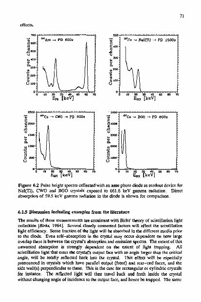
effects.
71
Tog' s " 'Am -» PD 600s
500-mCs -» N«[(T1) - • PD 1500s
caoo- c C C « f l «. . . us j - 8 0 0 - £ O u u.wo-_ fl 300-0) n / V a 1 a 300- L. 1 01 A M 2 0 0 - V/^ *
•*-> \ 1 Ci200- \ c 3 \ 3 O \ 1 I o loo- 1 I 1 O 100- ul_^J i
o I < ID 20 30 40 30 So" 70 i JO H) 30 40 SO SO 70 EP,, [keV] E3Ci [keV]
s cuooo
c 3 otooo-o
"Cs -» BGO -> PD 600s
JU 30 40 SO 00
[keV]
Figure 6.2 Pulse height spectra collected with an ame photo diode as readout device for Nal(Tl), CWO and BGO crystals exposed to 661.6 keV gamma radiation. Direct absorption of 59.5 keV gamma radiation in the diode is shown for comparison.
6.1.5 Discussion including examples from the literature
The results of these measurements arc consistent with Birks' theory of scintillation light collection [Birks, 1964], Several closely connected factors will affect the scintillation light efficiency. Some fraction of the light will be absorbed in the different media prior to the diode. Even self-absorption in the crystal may occur dependent on how large overlap there is between the crystal's absorption and emission spectra. The extent of this unwanted absorption is strongly dependent on the extent of light trapping. All scintillation light that enter the crystal's output face with an angle larger than the critical angle, will be totally reflected back into the crystal. This effect will be especially pronounced in crystals which have parallel output (front) and rear-end faces, and the side wall(s) perpendicular to these. This is the case for rectangular or cylindric crystals for instance. The reflected light will then travel back and forth inside the crystal without changing angle of incidence to the output face, and hence be trapped. The same

72
effect may, to some extent, occur in any layers in between the crystal and the diode. It is, however, very likely that more light will be lost through the sides of these layers as it is difficult to have any reflector arrangement there.
The light trapping is effectively reduced by using diffuse reflectors which changes the direction of the back-reflected light. White teflon tape [Holl et al, 1988; Grossmann et al, 1985b; Carrier and Lecomte, 1990; Safari, 1987; Markakis et al, 1985], aluminum foil [Hall et al, 1986; Keil, 1968; Goyot et al, 1988] and various paints based on MgO [Sakai, 1987], BaS0 4 [Sakai, 1987; Markakis et al, 1985] and TiO [Keil, 1968; Bateman, 1969; Glasow et al, 1985] have been successfully used as reflectors with approximately equal efficiency. Even white paper and typist's white correction fluid has been used with relatively good result [Blånar et al, 1982]. Birks [1964] also suggests evaporated aluminum as reflector, and he emphasizes the importance of having an efficient reflector especially on the rear-end face of the crystal.
The fraction of reflected light is reduced by increasing the critical angle of the different optical interfaces between the crystal and the diode. The mission of the optical coupling compound is to optimize the matching of refractive indices and thereby reduce the reflectivity and increase the critical angle. Silicon grease is used as coupling compound in most of the literature references listed above, but there is also a few examples v/here silicon oil has been applied [Keil, 1968; Sakai, 1987]. Most interesting is, however, the more permanent coupling methods where the crystals are glued onto the diodes with epoxy or equivalent [Grossmann et al., 1985b; Goyot et al., 1988]. The combined mission of coupling compound and diode surface protection reduces the number of optical interfaces the scintillation light has to penetrate, by one. This should result in a reduced possibility of both light trapping and loss through the sides.
Concerning light loss through the sides of the optical layers between the crystal and the diode, a few precautions can be taken. If possible, it is an advantage to use a diode with somewhat larger area than the output face of the crystal [Holl et al., 1988]. Any epoxy coating of the diode assembly which is outside the area covered by the crystal, should be covered by a reflector. If the diode housing in addition is white, this will result in a reduced light loss as some of it will be scattered back into the active diode area [Blånar, 1982].
Table 6.3 gives a summary of the scintillation light collection efficiency, TD/QC, of some examples found in the literature. All these values arc measured by exposing the crystals to Y-radiation, and they are given relative to the corrected Q c results of Holl et al. [1988]. Some of these Q c reference values seem to be somewhat underestimated as the calculated collection efficiency in some cases exceeds 100% [Carrier and Lecomte, 1990; Sakai, 1987]. This may be due to slight differences in fabrication processes, even if there also may be variations in the Q c-values of crystals within the same batch [Holl et al., 1988; Sakai, 1987]. The lack of knowledge about the accurate Q c-values for each particular crystal mskes it difficult to draw a conclusion based on the comparison in table 6.1. According to the measurements in this work, however, it seems to be relatively easy to achieve a scintillation light collection efficiency of about 55% when optical grease is used on top of an epoxy coated diode. This value may be further increased towards 80% when the system is optimized with respect to low trapping, absorption and loss of light prior to the diode. This means that the quantum efficiency of the diode, O e , is the only limiting factor.

73
Reference Cryslal Reflector Diode Optical coupling
Keil [1968) CsI(Tl) Aluminum Si (QE=60% al 500nm) Oil 34.4
Markakis el al. [1985J NaI(Tl) DaS04 Hgl2 (EG&G/EM) Grease S6.4
Grossmann et al. [1985a] Cs[(TI) ? Si? 7 75.8
Grassmam et al. (1985b] CslfTl) Teflon lape Si (Ham. S-1790-01) Epoxy 96.6
Canier and Lccomte [1990]
BGO NalfTI) Csl(Tl) CWO
Teflon lape Si avalanche (RCA Inc.) Grease 87.6 41.5 109.0 142.5
Sakai [1987]
iSisi
MgO Teflon tape Teflon tape RaS0 4
BaSO,
Si (Ham. S-1790-02) Oil Grease Grease Grease Grease
39.3 65.9 108.7 86.9 62.3
Table 6.3 Summary of experimental scintillation light collection efficiencies, Tg/Qp. The values arc given relative to the quantum efficiency values given by Holl et ai 11988].
6.2 Energy resolution in scintillation crystal detectors The greatest restriction in the use of detectors based on scintillation crystals is their Door energy resolution, R, which is a serious limitation on the resolving power for y-radiation. It is, in contrast to the noise analysis of the silicon diode in chapter 5, very difficult to do a similar analysis of a SC based detector. The physical phenomenas taking place in both the scintillation process and the light transmission to the optical readout device, is relatively well known. It is, however, almost impossible to predict the accurate magnitude of their contributions to the total line-width (FWHMS C). This may be seen by analogy with the need of an energy calibration to determine the relationship between pulse height and energy for a PMT scintillation counrc- This cannot be predicted even if the gain of the PMT is known [Miyajima et al., 1984], In the following inorganic crystals will be considered only.
6.2.1 The composition of line-widtb in a scintillation crystal - photo multiplier tube detector
The factors contributing to the observed line-width of a PMT scintillation counter, may, according to flints [1964], be summarized as follows:
(i) Emission of photons by the scintillation crystal
(ii) Collection of scintillation-photons by the photo cathode
(iii) Emission of photo-electrons by the photo cathode and collection of

74
these electrons at the first dynode
(iv) The electron multiplication process
Concerning photo diode readout of the scintillation pulse, only (i) am (ii) are of interest. Hence, attention will be paid to these only. The contributions (iii) and (iv) may be found experimentally and separated from the total line-width. This is done by injecting light pulses on the PMTs entrance window as described by Prescott and Takhar [1962], for instance. Note that (ii) could also be expressed as the transmission of scintillation photons from the crystal to the cathode (or diode).
There may be local variations in the scintillation efficiency, Q c , of the crystal, due to a non-uniform distribution of activator ions, crystal defects or flaws. All these contribute to the variance of (i), but even a homogeneous crystal without any defects or flaws will have an "intrinsic" variance: A fraction of the x-ray energy deposited in the crystal will in all the absorption processes discussed in chapter 3.2.1, be transferred to electrons. The scintillation light produced per unit electron energy, dL/dE e, is not proportional to the electron energy, E e . Low energy electrons have a larger dL/dE e. Hence, if the total energy is equal, many low energy electrons will give a larger total light output than few high energy electrons [Iredale, 1961]. Consequently there will be a spread in light output depending on the distribution in number and energy of electrons involved in the absorption. This distribution is dependent on the type of interaction processes taking place by the absorption of the incident y-quantum and secondary radiation. In contrast to photo-electric absorption, Compton absorption produces electrons which arc statistically distributed both in number and energy'1. Small crystals will due to this have lower intrinsic line-width than larger ones. This is because the photo-electric interaction process makes the most important contribution to the total absorption in small crystals. Deposition of the full energy of a v-quantum by Compton interactions is unlikely in a small crystal since a larger fraction of secondary y-quanta escapes the crystal [Zerby et al, 1961].
A further contribution to (i) arises from fluctuations in the secondary electron production. The electrons generated by any of the primary interaction processes, may loose their energy either by directly exiting atoms within the crystal, or by ionization where secondary electrons are produced. These secondary electrons, also called 8-rays, will have statistically distributed energies ranging from a few eV up to the full energy of the primary electron. This will, by the same reasoning as above, give rise to a further broadening of the line-width [Iredale, 1961]. Note that both these effects originating from the non-linear dL/dE^^-relationship for electrons, causes a non-normal scintillation variance. This means that the relationship where the line-width (FWHM) is given as 2.35a (the variance=a2), is no longer valid [Birks, 1964].
Self-absorption, reflection losses, light trapping and eventual optical flaws will give contributions to (ii). All these effects will, as discussed in section 6.1.5, reduce the scintillation light collection efficiency. Only by making the collection efficiency as constant or near unity as possible, the variance of it is minimized. This variance is
^ The production and rc-absorption of Brcmsstrahlung x-rays in photo-electric interactions arc found to have neglibilc contribution to the intrinsic line-width [Iredale, 1961].

75
found to be energy dependent since y-rays of different energies interact with different probability at different depths in the crystal [Prescott and Takhar, 1962]. A low energy y-quantum is likely to interact close to the input surface of the crystal. Any factors that limit the light transmission in the crystal, will have larger influence on the light collection of a low energy quantum than that of a high energy y-quantum which more likely interacts closer to the output surface.
6.2.2 Energy resolution in a NaI(TI) - photo multiplier tube detector
The composition of the line-width of the NaI(Tl) crystal has been subject to many both theoretical and experimental studies. This is, of course, related to the wide-spread use of this crystal combined with PMTs over a long period of time. The results of these studies should, however, to a large extent be applicable for the evaluation of other inorganic crystals too. An example of the composition of the total energy resolution, r) T (»R), for y-rays in a NaI(Tl) PMT scintillation counter, is given Prescott and Takhar [1962] and shown in figure 6.3. The experimental values of r^ and the squared contribution from the PMT are given in the upper curve and curve P, respectively. Curve A is T)| corrected for fluctuations in the production of electron spectra, while further corrections for fluctuations in 6-ray production arc also included in curve B. These intrinsic"' contributions are found by Monte Carlo simulations where the function which describes the non-proportional response of NaI(Tl) to electrons, are found experimentally [Zerby et ai, 1961]. A final curve C, which also includes corrections for the PMT-resolution (curve P), represents the contributions of (ii).
Narayan and Prescott [1968] have found, also by MC simulation, the contribution of the intrinsic broadening to be somewhat larger, and they summarize the energy dependence of the different contributions as follows: The intrinsic contributions (i) dominates T|T for y-energies between 450 keV and 1 MeV, while in the energy region 150 to 450 kcV a considerable fraction of % is to be attributed to the fluctuations in transmission (ii). They also point out that fluctuations arising from the surface treatment of the crystal feces, arc dominating T|T for y-energies below 150 keV [Narayan and Prescott, 1966]. It should, however, be natural to include this effect under the above (ii)-contribution as it probably is related to fluctuations in reflections and light trapping
RECIPROCAL. E N E R G Y — M E V ' 1
Figure 6.3 Composition of energy resolution in a NaI(Tl) - photo multiplier tube detector. The figure is adopted from Prescott and Takhar [1962].
k ) Only the first of these contributions, fluctuations in the production of electron spectra, is in many cases lefenred to as intrinsic broadening. This, in spite to tnc fact that the latter, fluctuations in the production of 6-rays, is a typical intrinsic effect as well.

76
in the crystal. These effects are discussed in section 6.1.5. Best result, that is lowest contribution to %, was achieved with finely grounded surfaces.
6.2.3 The composition of line-width in a scintillation crystal - photo diode detector
The composition of the total line-width in a SC-PD detector may be regarded in a similar manner as that of the SC-PMT. The only difference is that the contributions from the PMT, (iii) and (iv), are replaced by the total electronic noise of the PD and the preamplifier, EE, which is defined in chapter 5. If E c is defined as the "noise" arising from (i) and (ii), as discussed in the previous section, the total line-width (or noise) of a SC-PD detector can be expressed as:
E ^ c - E å s c + E l s c - E ^ f ^ V
(6.1)
where the additional subscripts SC and PD denotes whether the calibration is based on deposition of y-energy in the crystal or the diode, respectively. The ratio between these calibrations equals the energy-transfer efficiency, T D so that E E ^ E E ^ / T E . The electronic noise in the photo diode and preamplifier, Ej, is to a good approximation independent of the incident y-energy, E,. This is in contrast to the electronic noise of the PMT which, according to figure 6.3, is proportional to v'E,. This is illustrated tor a NaI(Tl) crystal in figure 6.4 where the composition of the total line-width in both the SC-PMT (dotted lines) and SC-PD (dashed lines) configurations are plotted. The data of the total and electronic line-widths of the SC-PMT configuration, marked as Ef™ and El 1 " respectively, are taken from figure 6.3. The line-width arising from the NaI(Tl) crystal alone, E c
(solid line), has been calculated from these data. These values of Ec has further been adopted for the SC-PD configuration for which the total line-width, EfD, has been calculated after equation 6.1. The electronic noise of the diode, EE
D, is found based on the specifications of the ame diode described in section 6.1.2 (£,^=2.5 keV FWHMn,, Qc=80%), and the scintillation efficiency of Nal(Tl) in table 6.1 (0^=11.3%). It is further assumed that the scintillation light collection efficiency is limited by the quantum efficiency of the diode only, that is; TB=QeQc-9.0%. Hence, the plot of E£D represents a minimal line-width which in an experiment may be obtained under optimal conditions only. The SC-PD experiment with the NaI(Tl) crystal in this work resulted, as described in section 6.1.4, in a total line-width of Ej-100 keV FWHMsc it £,=661.6 keV. This large line-width is due to the energy-transfer efficiency which, due to large optical mismatch, was as low as
Figure 6.4 Composition of the total line-width in a SC-PMT detector (dotted lines, data as in figure 6.3), and in a SC-PD detector (dashed lines, calculated values based on Ec from the SC-PMT data).

77
TE=3.4%. Anyway, according to figure 6.4 it should be reasonable to conclude that the SC-PD configuration gives the best energy resolution for y-energies above, say 500 keV. It is difficult to find any verifying data on the energy resolution in scintillation crystal - photo diode experiments with NaI(Tl) crystals.
6.2.4 Line-width in a CsIfTI) - photo diode detector
The Cslfn) crystal is, due to its high Q c and excellent spectral matching to photo diodes, used for the majority the scintiPation crystal - photo diode experiments. The NaI(Tl) and CsI(TI) crystals can, however, easily be compared concerning energy-transfer efficiency and energy resolution. Some examples of energy resolution in SC-PD experiments with CsI(TI) crystals are shown in figure 6.5. The solid line which represents the total energy resolution of a CsI(Tl)-PMT detector with S-20 response, is shown for comparison. The corresponding values of E^,,, T E and E^sc are listed next to the size of the crystal for each experiment. The relatively large variations in these values between the different data sets causes the large deviations in the experimental values of R. The contribution of E c to the total line-width has been calculated for two of these experiments, and the results are plotted in figure 6.6. Both these crystals have rectangular shape with 10x10 mm 2 output faces, and Hamamatsu diodes as readout detectors. They only differ in length, one crystal is 7 mm (solid line) while the other is 24 mm (dashed line). There is still some deviation in the line-widths, including a weak difference in energy dependence. It is, however, difficult to know whether this
IN?
K a o 3 1 0 . -o w <D i-,
Si <v a
\
Size[mrn 3]/EE r o/T,[%]/EE. ! K :/Ref. « « 4 # 10x10x24/3.4/11.6/29.4/b • BUDO 0-18x22/?/9.O/?/b,a • • • • • 10*10*7/4.3/12.9/33.3/c • • • • • 0-2.5*3/5.O/4.O/123.O/d 00000 9*9*~3 (truncated pyramid)/
3.2/11.9/26.9/e All E r in keV FWHM
C-OOc-c- 15xl5xl0mrrT on S20 PMT, Grassmann et al. [1985] 1 1 1 i 1 1 1 1 1 1 1 1 1 1 1 1
500 1000 1 1 1 1 1 1 1 1 1
1500 -TTTTTTT
2000 2500 3000
E7 [keV] Figure 6.5 Experimental values of energy resolution in CsI(Tl)-PD detectors. a;b) [Grassmann et al., 1985a; 1985b), c) [Sahai, 1987], d) [Keil, 1968], c) [Holl et ai, 1988].

78
is
>
W
is caused by the different crystal lengths, or by any of the other factors listed in (i) and (ii) in section 6.2.1.
It is interesting to compare these results with the more accurate calculation of E c
for NaI(Tl) which is plotted in figure 6.4. The energy dependence seems to be approximately the same, but the E c -va l -ues of NaI(Tl) seems to be about 50% larger than those of CsI(Tl). It is very likely that this difference can be explained by the larger size of the NalfTl) crystal (0=38.1x31.8 mm3), even if there also may be individual differences between the to crystal types. All together, the results plotted in figure 6.5 confirm the conclusion of the previous section: The SC-PD detector with any of these crystals and v noise readout electronics (E^-3 keV FWHMP D), is superior to the SC-PMT detector concerning energy resolution for y-energies above about 500 keV. This energy limit increases when crystals with lower TE-values, such as BGO or CWO, is used. A rough comparison of an extrapolation of Sakai's [1987] SC-PD results with SC-PMT data given by Harshaw [1984] confirms this: For BGO crystals the energy resolutions for these two configurations are equal at about 3.5 MeV y-energy.
500 1000 1500 E 7 [keV]
Figure 6.6 Calculated contributions of two CsIfTl) crystals (E^ to the total detector line-width (figure 6.5). Circles: [Sakai, 1987], triangles: [Grassmann et al„ 1985b].
63 The scintillation crystal - photo diode configuration, conclusion The relatively large uncertainty related to the collection efficiency of the scintillation light makes it very difficult to do accurate energy and noise analysis of the SC-PD detector. The collection efficiency determines the energy-transfer efficiency, T& which is the fundamental factor in this configuration. An increase in T E increases the output pulse height and reduces the influence of the diode and preamplifier noise. Concerning energy resolution, experiments show that it becomes advantageous to use the PD in stead of PMT for energies above about 500 keV for NaI(Tl) or CsI(Tl) crystals. This energy limit will be approximately halved to about 250 keV when the electronic noise of the diode and the preamplifier, 1%, is halved to about 1.25 keV FWHM r D as discussed in chapter 5.4.
In addition to the energy and noise considerations, the SC-PD detector has some other interesting features that makes it advantageous. It is more compact and robust than the SC-PMT detector, and it is, in addition, insensitive to electric and magnetic fields. Due to its compactness this detector can be easily stacked so that position sensitivity is achieved. This will be discussed in chapter 8. Further, no stabilized high voltage is needed for operation of the SC-PD detector, and this removes any drift in output pulse height. In contrast to the PMT a low noise charge sensitive preamplifier is needed for optimal operation of the PD, and this is of course a disadvantage.

79
Chapter 7
Theory and practical realization of the Electron diode photo multiplier tube
The drawback with the scintillation crystal - photo diode concept discussed in chapter 6, is that no compensation is made for the large fraction of the incident radiation energy that is lost in the scintillation process. This gives, relative to the incident radiation energy, rise to an increased low energy limit compared to that of the diode alone. In low flux applications the result is an energy gap between about 15 and some hundred keV where the diode, as a bare detector or as readout device for scintillation light, is unusable. The low energy limit of the scintillation crystal - photo diode combination, may be reduced to about SO keV by using smaller diodes (and crystals) and improved preamplifiers. At time being, however, it seems to be unrealistic to achieve an energy overlap with these two detector configurations.
One possible solution is to use avalanche photo diodes (APD) where the internal gain compensates for the energy lost in the scintillation crystal. The.fabrication of APDs involves process steps which make it difficult to achieve detector areas larger than some tens of mm 2. Carrier and Lecomte [1990] have used 25 mm 2 APDs in combination with CsI(TI) crystals, and the 5.9 keV line of s s Fe is for the first time visible with the crystal - diode configuration. This is indeed very good, and it is no doubt that this technology will be even more attractive if larger APDs can be made. Other problems with the APDs are temperature instability and low production yield.
Another possible solution is to make a compact detector which incorporates an energy multiplication section between the scintillation crystal and the diode. This is the idea behind the development of the EDPMT (Electron-Diode Ehoto-Multiplier-Iubc).
7.1 Theory of the EDPMT The EDPMT is a photo multiplier tube where the dynodes and the anode have been replaced by an electron diode. Hence, it is maybe more comparable to a vacuum photo diode. It has turned out that this concept is not new, it was first described by Abrahcm et al. [1966]. This was, however, before the planar oxide passivation process described in chapter 2.1 was developed, and the diodes at that time had a leakage current of the

80
order of 1000 times larger than those of today. Abraham et al. conclude that better protection of the pn-junction of the diode, especially against cesium and other active materials which are present in the photo cathode (PC), is necessary.
Scintillation crystal
Optical window
7.1.1 Principle of operation
A schematic drawing which illustrates the EDPMT principle of operation, is shown in figure 7.1. In the figure a scintillation crystal is used as a typical example of light source, but it is of course not the only applicable light source. TV incident light will impinge on the semitransparent PC through the entrance window of the tube. These photons cause emission of electrons with an efficiency QP. This is the quantum efficiency of the PC which is defined as the ratio of number of impinging photons to the number of emitted electrons. These electrons are accelerated over a potential V A and directed into the electron diode with an efficiency Q P E
(EC-*ED). This is the collection efficiency of the acceleration process, and it is defined as the ratio of the number of collected electrons in the ED to the number emitted from the PC. Each of the electrons entering the EL) will loose an energy AE in the ED's dead layer. The remainder energy will be absorbed in the active volume of the ED and contribute to its output signal.
El
X 11J | Photo Cathode " • . ! -«-Accelerating t i : t electrons
' ,r Electron Diode
Figure 7.1 Schematic illustration of the EDPMT operation principle.
7.1.2 Gain, G Q
The gain of the EDPMT is defined as the ratio of the ED signal current to the electron beam current, or more specific, the ratio between the number of electrons emitted from the PC and the number of electron Dole pairs created in the electron diode0:
QPE(SVA-AE) (7.1)
where V A is the acceleration voltage and c the electron charge. Hence, eV A is the average energy of each electron after the acceleration process. Further, w is the average energy required to create one electron hole pair in silicon. Due to the measurements in chapter 4.5.3 it is obvious that the LEPD meets the requirements as an electron diode. It was established by measurements that the dead layer energy loss, AE, at an initial electron energy of E„=10 keV, was about 0.8 keV only. Hence, the energy loss, AE, in equation 7.1 is adopted from these measurement results which arc plotted in figure 4.11. The best fit curve to these measured values and the extrapolation of this curve towards lower energies can be expressed as AE-8EJ1 (keV-units). Further, also note that the LEPD's sensitivity to light does not represent any problem inside an EDPMT where it is no ambient light. A practical EDPMT will have some kind of electro-magnetic focusing lens to assure that most of the photo electrons emitted from the PC, will reach
0 Note that all quantities given in % in ihis wotk are supposed 1o be convened to their absolute values when used in equations and calculations.
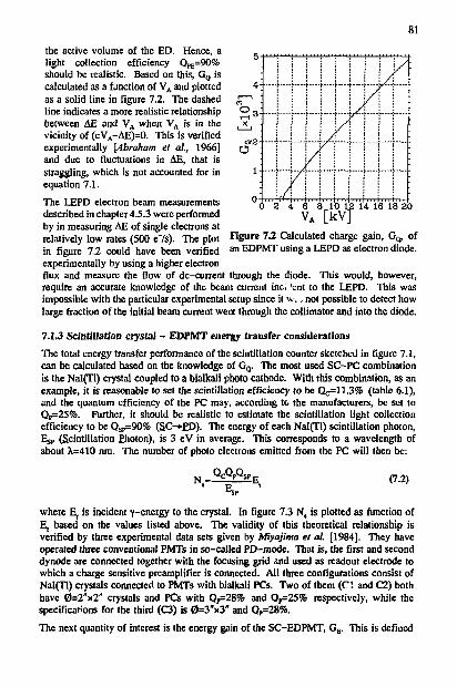
81
the active volume of the ED. Hence, a light collection efficiency QPE=90% should be realistic. Based on this, GQ is calculated as a function of V A and plotted as a solid line in figure 7.2. The dashed line indicates a more realistic relationship between AE and V A when V A is in the vicinity of (eVA-AE)=0. This is verified experimentally \Abraham et al, 1966] and due to fluctuations in AE, that is straggling, which is not accounted for in equation 7.1.
The LEPD electron beam measurements described in chapter 4.5.3 were performed by in measuring ÅE of single electrons at relatively low rates (500 e7s). The plot in figure 7.2 could have been verified experimentally by using a higher electron flux and measure the flow of dc-current through the diode. This would, however, require an accurate knowledge of the beam current inc, 'cnt to the LEPD. This was impossible with the particular experimental setup since it w.; not possible to detect how large fraction of the initial beam current went through the collimator and into the diode.
7.1.3 Scintillation crystal - EDPMT energy transfer considerations
The total energy transfer performance of the scintillation counter sketched in figure 7.1, can be calculated based on the knowledge of GQ. The most used SC-PC combination is the NaI(Tl) crystal coupled to a bialkali photo cathode. With this combination, as an example, it is reasonable to set the scintillation efficiency to be Qc=11.3% (table 6.1), and the quantum efficiency of the PC may, according to the manufacturers, be set to 0P=25%. Further, it should be realistic to estimate the scintillation light collection efficiency to be Qs|,=90% (SC-»ED). The energy of each NalfTl) scintillation photon, Ejp (Scintillation PJioton), is 3 eV in average. This corresponds to a wavelength of about X=4W nm. The number of photo electrons emitted from the PC will then be:
Figure 7.2 Calculated charge gain, an EDPMT using a LEPD as electron diode.
N ~ 2 £ A P E (7.2)
where E, is incident y-energy to the crystal. In figure 7.3 N, is plotted as function of E, based on the values listed above. The validity of this theoretical relationship is verified by three experimental data sets given by Miyajima el al. [1984]. They have operated three conventional PMTs in so-called PD-mode. That is, the first and second dynode are connected together with the focusing grid and used as readout electrode to which a charge sensitive preamplifier is connected. All three configurations consist of NaI(Tl) crystals connected to PMTs with bialkali PCs. Two of them (CI and C2) both have 0=2"x2" crystals and PCs with Q,=28% and Q,=25% respectively, while the specifications for the third (C3) is 0=3"x3" and Q,=28%.
The next quantity of interest is the energy gain of the SC-EDPMT, GE. This is defined

82
500 1000 E7 [keV]
1500
Figure 13 Number of photo electrons from a b i -alkali PC connected to a NaI(Tl) crystal. The dashed line is calculated due to equation 7.2, the markers represent experimental data [Miyajima et al, 1984].
as the ratio of energy deposited in the electron diode to energy, E,, incident to the scintillation crystal, and it may be expressed as:
(73)
where G E also may be regarded as the energy transfer efficiency of the SC-EDPMT analogous to T E defined in section 6.1.2 for the SC-PD detector. For the particular example given above G ^ O - I O - ' G Q . An acceleration voltage of 5kV gives G E - 2 5 , that is, a y-energy of S keV which is just on the limit of what can be detected directly in a photo diode, will be raised to about 125 keV when this SC-EDPMT is used.
7.1.4 Line-width of the scintillation crystal - EDPMT detector
The drawback with the SC-EDPMT configuration is the same as for other SC-detectors; the relatively poor energy resolution. The factors contributing to the line-width in the SC-EDPMT are, to a large extent, the same as those of the traditional SC-PMT as listed in section 6.2.1. The situation is identical concerning (i), emission of photons from the crystal, and (ii), collection of these photcus at the cathode. The contribution from (iii), emission of photo electrons from the cathode and collection of these at the firs) dynode, should have a comparable term in the SC-EDPMT where the photo electrons arc collected in the ED. Hence, only the contribution from the electron multiplication process in the PMT, (iv), is not present in the SC-EDPMT. The SC-EDPMT will, on the other hand, have a smalt contribution, E*. from fluctuations or energy straggling in the dead layer energy loss, AE. This effect was discussed in section 4.2.1. The magnitude of Ew was, due to unidcal noise conditions, not possible to

83
determine from the electron beam measurements described in section 4.5.3. It is, however, likely that contribution of r^ to the total line-width in the SC-EDPMT, is less than the contribution of (iv) to the total line -width in the SC-PMT. The electronic noise in a SC-PMT preamplifier is, due to the large gain of the PMT, neglibile compared to the contributions from (i)-(iv). Hence, the total line-width of the SC-PMT, Epun, is adopted as the line-width caused by statistical fluctuations in the signal of the SC-EDPMT. This should certainly not be an under-estimation of the latter since, as discussed, the contribution from (iv) in the SC-PMT probably is larger than E„ in the SC-EDPMT.
Some experimental data on EpM T
have been collected and are presented in figure 7.4. In addition to the CI, C2 and C3 configurations which are referred to in the previous section, two other data sets, also from experiments with Na[(Tl) crystals in combination with bi-atkali PCs, are plotted. The stars represent data collected with a 10x10x20 mm3 SC and Qp=28% [Sakai, 1987], while the solid squares represent the data also referred to in figure 6.3 [Prescott and Takha;, 1962]. The solid line may be regarded as a best fit line to the experimental values, but it covers, in addition, the "typical values" listed by Harshaw [1984] in their catalogue.
Based on the above assumptions the total line-width of the SC-EDPMT, where also electronic noise of the diode and the preamplifier is considered, can be expressed as:
Er.sc-EpMT-.sc+E&sc ErMT.sc*
where E j ^ and E^ea >s t 0 , a ' electronic noise based on energy deposition in the scintillation crystal and the electron diode, respectively. Note the analogy to equation 6.1. The interesting quantity here is the squared ratio of E ^ to E ^ since this expresses the relative influence of E^JC on E ^ . Figure 15 shows a plot of this ratio as function of the fundamental parameter V A and for Eg^-values ranging from 3 to 50 keV FWHM. The function AEfV J has been calculated in similar manner as for the solid line plot of GQ in figure 7.2. Some electrons may, due to fluctuations in AE, penetrate the dead layer with energies down towards eVA=2 kcV. This means that the real (EE.SC/ETJC)2 will be less than the plotted one for VA-valucs less than, say 3.5 kV. The plotted ratio has been calculated at E,=3 kcV, that is the energy of the incident
500 1000 E7 [keV]
1500
Figure 7.4 Experimental values of the total line-width in a NaI(Tl) - bialkali photo cathode detector. The solid best fit curve represents typical values given by Harshaw [1984], too. For further references, see text.
(7.4)
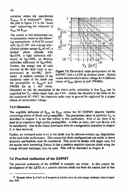
84
radiation where the contribution EpMT.sc i s a ' minimum™'. Hence, the plot in figure 7.5 is the "worst case" concerning the influence of EE.SC o n ET.SC-
The results in this estimations are, to summarize, based on the following assumptions: A NaI(Tl) crystal with Q c=11.3% and average scintillation photon energy EsP=3 eV, a bialkali photo cathode with QP=25%, a light collection efficiency of Qsp=90%, an electron collection efficiency of Q f E=90%. Further, the energy loss of each electron in the dead layer is approximated as AE=8Eo" (keV-units). A realistic estimate of the electronic noise of the diode and the preamplifier is 5 ^ = 3 keV FWHM for an 1 cm 2 diode. Grounded on this the conclusion of the above noise estimation is that E ^ can be neglected for VA-values larger than, say 4 kV. Hence, the situation is the same as for the traditional SC-PMT, the electronic noise may in general be neglected by a proper choice of acceleration voltage.
7.1.5 Discussion
The neglibile influence of E^sc on E ^ makes the SC-EDPMT detector flexible concerning choice of diode and preamplifier. The precautions taken to minimize Ep, as described in chapter S, is not that critical in this application. First of all, there is no need of an expensive high quality preamplifier. A twice as noisy, low cost device will be satisfactory. One of the major drawbacks with the configuration described in chapter 5, is then removed.
Further, an increased noise level in the diode may be allowed without any degradation of the total noise performance. This means that diode configurations not usable in direct detection applications, may be considered. This could be diodes with larger area, but the maybe most interesting feature is that a position sensitive electron diode using the charge division technique, may be used. This will be discussed in chapter 8.
12 Practical realization of the EDPMT The practical realization of the EDPMT is certainly not trivial. In this project the development of the LEPD as a suitable electron diode has been the easiest part of this
B ) Energies below 1^3 keV is of no practical interest since the tola! energy resolution there is larger than 50%.
Figure 7.5 Theoretical noise performance of the EDPMT with a LEPD as electron diode. Plotted versus electron acceleration voltage for 6 different values of E ^ D (given in keV FWHM).
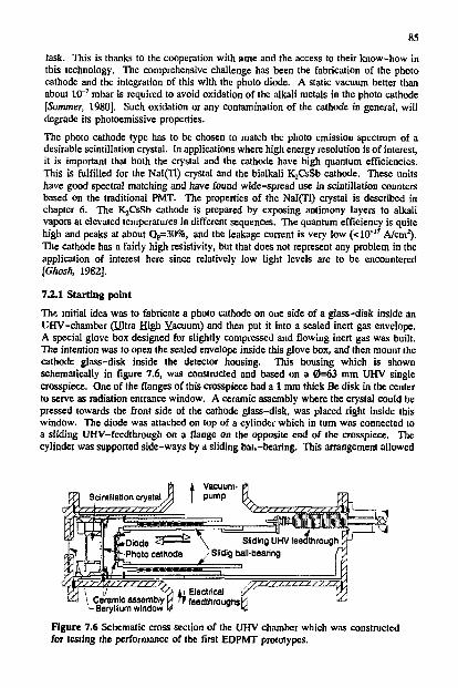
85
task. This is thanks to the cooperation with ame and the access to their know-how in this technology. The comprehensive challenge has been the fabrication of the photo cathode and the integration of this with the photo diode. A static vacuum better than about 10~7 mbar is required to avoid oxidation of the alkali metals in the photo cathode [Sommer, 1980]. Such oxidation or any contamination of the cathode in general, will degrade its photoemissive properties.
The photo cathode type has to be chosen to match the photo emission spectrum of a desirable scintillation crystal. In applications where high energy resolution is of interest, it is important that both the crystal and the cathode have high quantum efficiencies. This is fulfilled for the NaI(Tl) crystal and the bialkali K2CsSb cathode. These units have good spectral matching and have found wide-spread use in scintillation counters based on the traditional PMT. The properties of the NaI(Tl) crystal is described in chapter 6. The K2CsSb cathode is prepared by exposing antimony layers to alkali vapors at elevated temperatures in different sequences. The quantum efficiency is quite high and peaks at about QP=30%, and the leakage current is very low (<10"17 A/cm2). The cathode has a fairly high resistivity, but that does not represent any problem in the application of interest here since relatively low light levels are to be encountered [Ghosh, 1982],
72.1 Starting point
The initial idea was to fabricate a photo cathode on one side of a glass-disk inside an i;HV-chamber (Ultra High Y_acuum) and then put it into a sealed inert gas envelope. A special glove box designed for slightly compressed aud flowing inert gas was built. The intention was to open the sealed envelope inside this glove box, and then mount the cathode glass-disk inside the detector housing. This housing which is shown schematically in figure 7.6, was constructed and based on a 0=63 mm UHV single crosspicce. One of the flanges of this crosspiece had a 1 mm thick Be disk in the center to serve as radiation entrance window. A ceramic assembly where the crystal could be pressed towards the front side of the cathode glass-disk, was placed right inside this window. The diode was attached on top of a cylinder which in turn was connected to a sliding UHV-fecdthrough on a flange on the opposite end of the crosspiccc. The cylinder was supported side-ways by a sliding bal.-bearing. This arrangement allowed
V> i i Electrical \ Ceramic assembly H Tf - Beryllium window \f
Figure 7.6 Schematic cross section of the UHV chamber which was constructed for testing the performance of the first EOPMT prototypes.
86
for adjustment of the cathode - diode separation. The third flange of the crosspiece was reserved for electrical feedthroughs, and the fourth for the vacuum pump.
The aim of this experimental setup was to fabricate a photo cathode with 10% quantum efficiency. Based on a general description of preparation methods for semitransparent photo cathodes given by Sommer [1980], an experimental arrangement was prepared at the Max-Planck-institut fur Aeronomie in Katlenburg-Lindau, FRG. Figure 7.7 gives an overview of the setup. The glass-disk was mounted in the center of a double UHV crosspiece in such way that it could be rotated to face either the optical window during tests or the evaporation sources during evaporation. A conical stainless steel plate with a hole was used as anode during the tests, and the light source was an ordinary car bulb in front of a monochromator. The spectral photo current was measured with a picoammeter at 100 V ar^de-cathode voltage. Two thermo-electric heaters were used to bake '.he cathode disk, and the total film thickness subsequent to each evaporation cycle could be monitored with a calibrated photo diode. Each evaporation source consisted of a 250 urn diameter W/Th wire winded around an Al 2O a cup in which the desired evaporation material could be placed. In the case of alkali metals this arrangement was placed inside a larger cup filled with high purity benzene.
Light source
t Vacuum-pumpH
\ z 3 El. feedthroughs
Heaters **
^Photo diode
Monochromator ' Photo cathodi
Glass disk
Evaporation—j£ shield
Evaporation -sources
i J f i ^ *Evapotation 1 1 3 3 0 sposføorTl[)
\
High current faedthroughs-*"
Figure 7.7 Cross section of the UHV chamber used for photo cathode fabrication.
The first step was to make opaque pholo cathodes on a stainless steel plate in order (o verify the setup. Several such cathodes based on bismuth (Bi) combined with cither sodium (Na). potassium (K) or cesium (Cs) were successfully made. None of them were, due to the relatively simple optical test equipment, calibrated in terms of quantum efficiency. The large drawback with all these cathodes, however, were their very short lifetime. Their photo currents were at maximum just after the last evaporation step, and then falling off rapidly with lime. This indicated that oxidation or contamination had taken place and that the vacuum conditions consequently was not good enough for a

87
stable cathode. The dynamic vacuum was, however, better than 10"7 mbar prior to the evaporation process.
The conclusion was that when this vacuum, which is the best obtainable with a cryogenic pump and high quality UHV equipment, is not satisfactory for fabrication of a stable cathode, the cathode will certainly not survive the inert gas transfer procedure as described above. Hence, the vacuum requirements for a stable cathode had been under-estimated, and the cathode fabrication had to be done another way. In practice this means a process comparable to that used for fabrication of photo cathodes in the traditional FMT, That is, the cathode has to be processed, baked and sealed in one operation. Thus, the detector housing has to be some kind of a tube which could be hermetically sealed, the crosspiece housing described above can certainly not be used. Further, this also means that the diode has to be present during the cathode processing. This set some more stringent demands for the diode. It is has to withstand the final baking process of the cathode with respect to both temperature and cathode residual gases. This baking process is standard in the fabrication of high performance photo cathode tubes to provide good life time properties.
7.2.2 Demands to the electron diode
The main protection of the diode pn-junction is the S i0 2 layer which is the central key in the planar process. In addition to this the oxide of the electron diode was coated with an about 1.8 urn thick polyimide layer as described in chapter 2.1.6. This layer is believed to be especially important in protecting the electron diode against the hazardous alkali metal vapour generated during the cathode baking process. This polyimide can, however, not be used without knowing its effect on the cathode. That is, it is equally important that the diode does not release any gases during the baking process that are hazardous to the cathode.
Due to this, two silicon wafers, one with polyimide and one without, were sent to English Electro Valve (EEV) Chemical and Metallurgical Laboratory in Chelmsford, Essex, UK, for a vacuum compatibility evaluation. The residual gases from the polyimide were found by comparison to the bare silicon wafer at temperatures up to 400°C. The test results is written in a report [EEV, 1989] which concludes as follows:
"The polyimide coated Si wafer, on initial pumping and low temperature heating, evolved large quantities of unidentifiable hydrocarbons. This feature was not retained on cooling and the material appeared vacuum compatible. Further heating to 400°C evolved, to a lesser degree, more hydrocarbons and again, on cooling, the polyimide permitted a very low base pressure. The effects of reheating and electron induced desorption (EID) are not known, of which, EID may be a significant factor in the decision as to the suitability of polyimide. After heating process only, polyimide may be suitable for incorporation in an image intensifier."
Here the reference to an image intensifier is equivalent to a photo cathode tube. That is, if the polyimide coated electron diode is properly baked in advance, it is usable for this application. Note, however, that ion pumps are not suitable for pumping large quantities of hydrocarbons as they exhibit a strong memory effect, and the pump performance is degraded. This is also mentioned in the above report, and it is
88
recommended that any outgassing system should include a liquid nitrogen cooled diffusion pump or a turbo molecular pump. Altogether it should be reasonable to conclude that the diode should be thoroughly baked and electron scrubbed before it is introduced into the vacuum tube. This may cause a degradation of the protection properties of the polyimidc, but as a compromise, this is the best solution.
The diode's resistivity to heating was examined in a vacuum oven. It was found that a diode with a gold layer contact on its backside, could withstand heating to 350°C for 48 hours without any deterioration of its noise performance. Heating to 380°C, even for shorter periods, will damage the diode. This is due to migration of gold into the diode bulk. It is reasonable that this version of the LEPD which has a Al layer contact on its backside, can withstand heating to even higher temperatures. Baking at 350°C for 48 hours is, however, satisfactory in this application.
. Input window
7.2.3 The detector tube
From the conclusion in section 7.2.1 it is evident that the cathode fabrication has to be done in a laboratory specialized for this task. Hence, a corporation project with the Tube and Sensor Laboratories at ITT Electro-Optical Products Division in Fort Wayne, Indiana, USA, was started. ITT suggested to use a modified image intensifier tube for the first EDPMT prototype samples. This tube, which is fabricated by ITT, is shown schematically in figure 7.8. ITT constructed the back-end piece of this tube especially for the EDPMT. The center of this piece is a glass-disk with several kovar pin feedfhroughs. Another glass-disk with kovar pins is mounted on top of this (pin-to-pin) inside the tube. This is the header which the diode is to be mounted upon. A 12.7x12.7 mm 2 Al layer was evaporated onto the top of this to serve as contact to the n* back side of the diode. The connection to this layer is a kovar pin through the center of the header. In addition, two smaller Al layers are evaporated on top of two other kovar pins outside the diode area. These are connected to the top p* layer of the diode through the bonding wires.
For the first EDPMT samples it was decided that the diode should be mechanically attached to the header. Any outgassing from an eutectic material which otherwise could be used to fasten the diode, will then be avoided. Four U-formed metal clips were inserted side ways onto the header and over the four comers of the Si chip. First these clips were made out of wrought beryllium-copper (Be-Cu) alloy 25 (CI 72) which is a common clip alloy with excellent spring properties. The clips were machined and then precipitation hardened at the recommended temperature and time, which is about 315°C for 3 hours. Next to cooling, the clips were mounted onto a metal disk equal in thickness to the header plus the diode, and then heated to 300°C for 8 hours. This was done to investigate how a baking process would affect the clips. The result was as suspected, the clips were only loosely attached to the metal disk after this treatment.
Header Glass l*Kovar pins
Figure 7.8 The EDPMT prototype tube which is under fabrication at ITT. The drawing is adopted from 77T [1989].

89
Hence, another Bc-Cu alloy had to be used. The procedure was repeated with some alloy 10 (C175) clips which precipitating temperature and time is about 482°C for 2 hours. There was no measurable change in the degree of attachment to the metal disk after the baking equivalent heating this time.
Hence, two diodes were then mounted on headers with Be-Cu alloy 10 clips. The leakage currents of these devices were measured to be about 500 pA at -60 V before and after mounting. As mentioned in chapter 2.1.4, ball bonded gold wires are normally used for the diodes. This is, however, not ideal in the EDPMT due to the high temperature treatment. This may cause connection problems in the Al-Au interface especially on the diode bonding pad. Thus, wedge bonded SO pm diameter Al wires were used. Two wires were used on each diode to provide an extra security. Some pictures of one of the diode headers are shown in figure 7.9.
Figure 7.9 Photographs of the EDPMT diode header before and after mounting of the diode. The shield (bottom, right) is used as bonding wire protection and clip retainer.

90
7.2.4 Discussion
The headers were fabricated at ITT in Fort Wayne, the clips at Department of Physics in Bergen, and the mounting and bonding of the diodes were done at ante in Horten. The two headers were then shipped back to ITT for cleaning and integration in the tube before the cathode processing could start. This has been a time consuming process and these first EDPMTs arc still not finished. Due to this, there is, unfortunately, no test results available from these tubes at the time being.
In the meantime, however, a Dutch company, Delft Electroninishe Produkten B.V., The Netherlands, has succeeded in fabricating a device similar to the EDPMT. They have named it "Hybrid Photo Multiplier Tube" (HPMT), and it was presented at the Second London Conference on Position-sensitive Detectors, September 4.-7. this year. The test results from this device looks very good indeed. The experimental data on gain as function of acceleration voltage matches the theoretical relation plotted in figure 7.2 with very good accuracy. Further, a 60 day life test of the HPMT showed only a weak decrease in the cathode sensitivity [van Geest and Stoop, 1990J.
These HPMT test results verifies, to a large extent, the theoretical predictions of the EDPMT which was derived in section 7.1. No doubt, this detector will be able to compete with the traditional PMT. The EDPMT have several advantages, most of them related to its smaller size which, for instance, will make it less sensitive to external magnetic fields. It is also reasonable to believe that the compact EDPMT will be a more robust detector. This is due to the elimination of the dynode chain. Last, but not least it should be a relative simple task to make the EDPMT position sensitive by using a position sensitive diode. This will be discussed in the proceeding chapter.

91
Chapter 8
Position sensitive detectors
There are several interesting applications for position sensitive nuclear radiation detectors. In some cases a device which is position sensitive in one dimension is satisfactory. Such a device can also be used to yield position information in more than one dimension if it is combined will some kind of motion. This may, for instance, be two dimensional information from a detector on board a spinning rocket or satellite, or three dimensional information from a tomograph detector where the specimen are rotated and moved forward. Position sensitivity in two dimensions are, however, most interesting as this is the fundament for different types of cameras.
A position sensitive silicon detector system is in its simplest form an array of discrete diodes. An overview of other, more advanced concepts are given by Radeka [1984] and Kemmer [1990]. To summarize, these are:
• The diode matrix detector
• The linear position sensitive detector using the charge division technique
• The integrated diode array also known as the microstrip detector
• The semiconductor drift chamber
• The fully depleted junction charge coupled device
The intention here is to demonstrate the techniques which can be applied to make the detectors discussed in chapter 6 and 7, position sensitive.
8.1 The diode matrix detector The diode matrix detector, which is an array of discrete diodes, is in spite of its simplicity worth paying attention to. This detector docs not, in contrast to the three latter devices listed above, have any electrodes crossing the radiation entrance window. The energy loss in such electrodes can be neglected in detection of high energy radiation such as minimum ionizing particles. The relative energy loss is larger for low energy radiation. This will give rise to an extra contribution to the total line-width of the detector because it, due to the small dimensions, is difficult to determine which of the events that have been partly absorbed. The diode matrix detector may be designed with an array of LEPDs or ordinary photo diodes depending upon the application.

92
Lately, most attention has been paid to the configuration where a photo diode array is coupled to one or several scintillation crystals. Concerning noise performance, this detector may be considered equal to the single SC-PD discussed in chapter 6. This is, however, on the condition that the crystal is optically divided into segments with areas equal or less than the area of each diode. It is important to distinguish between this configuration and the one where several diodes are coupled to one large crystal. The scintillation light can, in the latter case, be scattered over an area covered by several diodes causing a degradation of the signal to noise ratio. The extent of this effect will be determined by the physical sizes of the crystal and the diodes.
The position resolution of this detector is limited by the size of each diode segment, and can, of course, not compete with the other more advanced concepts. The relatively poorer energy resolution is, however, satisfactory in many cases. The array detector with crystals and diodes of equal size, has been proposed in several applications such as for instance radiography [Gupta and Krohn, 1987], industrial X-ray and y tomography [Ellingson and Vannier, 1987], positron emission tomography (PET) [Derenzo, 1984], and in astrophysics. The main advantage of this detector configuration is good packing density combined with high stopping power. It is, however, difficult to give an evaluation of the detector's over all performance as this will be strongly dependent upon each particular configuration. Crystal type, thickness and cell size, diode dimensions, SC-PD coupling technique, packing density and method, and finally readout electronics arc all important parameters in such an evaluation. The drawback in the need of a high quality preamplifier to achieve optimum noise performance, is even worse here since one preamplifier is required for each SC-PD segment.
A practical realization of this detector may be a ceramic plate with a printed metal pattern where the diodes are to be mounted. The integrated diode array detector, also known as the microstrip detector, may be regarded as an advanced, high resolution version of the diode matrix detector. The position resolution of this detector can be as good as 2 um, and it may be made position sensitive in two dimensions by using double sided strips [Kemmer, 1990]. This double sided device is, as mentioned, not suitable for detection of low energy radiation.
8.2 The linear position sensitive detector using the charge division technique
This principle requires diodes with a square resistive surfaces with one readout electrode on each of the four ends as shown schematically in figure 8.1. These electrodes form two parallel pairs, one in parallel with the X-axis on the back side and the other in parallel with the Y-axis on the front side. The X-position of an event is then, due to the resistive surface, determined by charge division between the electrodes on the front side and vice versa for the Y-position. Another version of these position sensitive devices have both the electrode pairs on the same side of the chip. Concerning the following noise estimation, however, these two versions may be considered equally.
A square LEPD is made position sensitive by lowering the implantation energy or dose so that the p* sheet resistance is increased to about 10 kQ/b- This will of course affect the dead layc.-, and, what is more important, the serial resistance, R s J, of the diode will increase. This detector requires four charge sensitive preamplifiers, one for each

93
Figure 8.1 Illustration of the linear position sensitive detector using the charge division technique.
electrode. The series resistance of a line emitter contact is estimated by Rowlings and Deighton [1989] to be R J d -G; J +RJ3 for frequencies up to [ihtCfGf+RJd)]-1. If the sheet resistance is RÆ=10k£J/n, each preamplifier will see a serial resistance RJj-3.3 kQ. This will, as shown in equation 5.10, generate a thermal noise, E,d, of about 6.1 keV FWHM in a depleted diode (G;'=0, T„=8 [JS). The total energy deposition in such a detector is determined by adding up the charge collected at the four electrodes. Hence, the total line-width will be even larger and may, as a rough estimation, approach 10 keV FWHM when the other noise sources are included, too.
This relatively large noise level excludes this detector from many applications where high energy resolution is required. Hence, this detector has, during the last years, been overshadowed by the other more advanced position sensitive silicon detectors, such as the microstrip detector and the drift chamber. Inside the EDPMT as a electron diode, however, this position sensitive detector is acceptable as it should not cause any increase in Erse when a proper value of V A is chosen (see equation 7.4). This diode has, like the matrix detector, the advantage of being position sensitive in two dimensions without any electrodes crossing the electron entrance window. This is of fundamental importance in this application since such electrodes will give rise to a variable dead layer thickness and thereby a variable energy loss in the dead layer.
This application of the linear position sensitive detector using the charge division technique, is demonstrated by Rougeot et al. [1979] and Roziere et al. [1981]. They have used this device as a "solid state localizer" in the second stage of a large image intensifier as shown in figure 8.2. Actually, this second stage is to a large extent comparable with a position sensitive EDPMT, except for the acceleration voltage which is 15 kV. A corresponding voltage of about 6 kV will probably be satisfactory for the EDPMT. Anyway, the input area of the first stage of this intensifier is about 935 cm 2
while the diode area is 12 cm2. This diode was operated at a capacitance of 300 pF and
94
u 1 s t Sugi F 0 , - l n i Cjlculitor Diipliv
Figure 8.2 The image intensifier camera with a "Solid State Localizer" in the second stage. The figure is adopted from Roiigeot er a!., [1979].
a maximum leakage current of 15 (iA. A spatial resolution of 4 mm was achieved with this intensifier and that is 0.4 mm relative to the diode [Rougeot et at., 1979]. This diode is certainly not a low noise device, and it is reasonable that the spatial resolution of a position sensitive LEPD will be better.

95
Chapter 9
Summary and conclusion
The primary aim of this project was to investigate the performance of silicon based detectors for low energy nuclear radiation and to advance in the development of such detectors. The three different detector concepts which have been considered are first the low energy particle detector (LEPD), second the photo diode as readout device for scintillation light, and third the electron diode photo multiplier tube.
9.1 Noise Low noise is a basic demand especially for the two first of these concepts. The noise level together with the energy loss in the diode dead layer, will determine the diode's lowest detectable energy. Diodes with depletion leakage currents less than 500 pA/^cm2) have been fabricated by the planar, ion implanted, oxide passivated process. The material has been 280 um thick with resistivity ranging from about 2 to 10 kQcm. The depletion series resistance of these diodes are, due to the high doping concentration achieved by ame's special implantation technique, less than 25 Q. Hence the total electronic noise of these diodes are less than about 1.5 keV FWHM.
The noise properties of the diode has to be seen in conjunction with the preamplifier and the noise of this. A state-of-the-art RC-feedback charge sensitive preamplifier has been constructed aad noise levels of about 1.2 and 2.0 keV FWHM have been achieved at 0 and 50 pF (depleted LEPD) input capacitances, respectively. Hence, a total diode and preamplifier noise of 2.5 keV FWHM has been achieved with this configuration.
All these numbers are referred to room temperature operation. The relative noise reduction obtained by cooling is, however, largest for the diode. Thus, the preamplifier noise will be even more dominant at lower temperature than it is at room temperature. The most obvious reduction of preamplifier noise is achieved by using diodes with lower capacitance. Hence, the diode active area has to be reduced and/or its thickness has to be increased. The first is no problem from a technical point of view, it will, however, be a drawback in applications with low radiation fluxes. The latter will increase the radiation stopping efficiency, but it is limited by the drawback of less efficient gettering processes. These are fundamental in order to achieve low diode leakage currents. The development of improved gcttering processes on thicker materials is, however, in progress. Recently 1 mm thick diodes have been processed on high resistivity (>8 kQcm) material at Center of Industrial Research (SI) in Oslo, and leakage currents of about 1.5 nA/cm2 are reported [Evensen, 1990], This is indeed very promising, and

96
attempts to make 2 to 3 mm thick diodes will be done. Another possible solution is to use silicon drift detectors where the capacitance is reduced to a minimum, often less than 1 pF. In these detectors an electric field provides lateral drift of the electrons liberated by ionization. They arc transported within the detector until they reach the readout electrode which is connected to the preamplifier. Rehak et al. [1989] reports on a spirally formed silicon drift detector where the capacitance of the readout electrode is 100 iF only. The drawback with the drift detector is the increased charge collection time due to the lateral drift time. A standard diode is preferable, especially if it can be made thicker without increasing the leakage current to much.
The conclusion concerning noise is that the largest overall reduction is obtained by reducing the intrinsic noise of the preamplifier. Noise arising from dielectric losses is the largest contribution to the total noise in the conventional preamplifier. This can be reduced by careful construction where a naked input field effect transistor (FET) is used. This FET-configuration also opens for other interesting feedback techniques such as optical feedback [Madden et at, 1990]. Hence, the next step in noise reduction should be a closer investigation of these factors.
9.2 Detector dead layer Concerning particle detection the energy loss in the dead layer is the second factor which define the low energy limit of the low energy particle detector (LEPD). The dead layer of the LEPD has been measured to be 64±8 nm. The corresponding energy losses at 10 keV incident radiation energy have been measured to 0.8 keV for electrons, and to 3.8 and 5.1 keV (nuclear energy loss included) for protons and He* ions, respectively. This is indeed very good. The theoretical energy losses of protons and He* ions are in good agreement with the measured ones even for energies as low as 10 keV. The theoretical energy loss is based on the continuous-slowing-down-approximation (CSDA) and it is further assumed that the particles enter the diode perpendicular to the surface and travel straight on through the dead layer without any deviation from this direction. These assumptions fail for electrons where the measured energy loss at 10 keV incident energy is about 3 times larger than the theoretical one. This is because the electrons, compared to the heavier protons and He* ions, will undergo more collisions where their direction are altered and hence have a total path which is longer than the dead layer thickness.
93 The silicon diode in combination with scintillation crystals The low energy particle detector is, due to the shallow dead layer, very well suitable as electron diode inside the electron diode photo multiplier tube (EDPMT). Even if there are no test results available yet, the EDPMT performance looks promising due to calculations and comparison with other analogous products. The diode and preamplifier noise in the EDPMT is believed to be neglibile compared to the noise sources. This opens for the use of position sensitive diodes using the resistive surface charge division technique, without any increase in the total noise. Neither should it be necessary to use a high quality preamplifier for the EDPMT. Compared to the traditional photo multiplier tube, the EDPMT also have a large advantage in being compact and robust.
A photo diode with the same parameters as the LEPD referred to in section 9.1, has been successfully used as readout device for scintillation light from several crystals.

97
The energy resolution of this device is better than that of the traditional scintillation counter for -y-encrgies above about 500 keV when a high quantum efficiency crystal, such as CsI(Tl), is used. This energy level will be reduced if the noise in the diode and preamplifier is reduced as suggested in section 9.1. The optical coupling technique between the crystal and the diode is especially important in this detector. Best results are obtained by gluing the crystal to the diode with an epoxy which also serves as protection of the diode. This is, as the EDPMT, also a very compact and robust detector compared to the scintillation counter based on the traditional photo multiplier tube.
9.4 Conclusion
An x-ray detector covering a broad energy range from a few keV to several hundred keV cannot be fulfilled in just one of the three detector concepts listed in the beginning of this chapter. The LEPD is suitable for the low energy region, and can be even better if the noise is reduced as proposed in section 9.1. For higher energies, say above 15 keV for the 280 urn thick LEPD, a detector with larger stopping efficiency is required, especially for low flux applications. Some kind of scintillation detector has to be applied. A scintillation crystal coupled to the EDPMT is a good alternative as this is a compact detector which is easily made position sensitive and which is believed to have an energy resolution equal to or better than the traditional scintillation counter. Hence, a low energy limit, that is where the energy resolution is about 50%, of about 5 keV may be expected with this configuration.
A scintillation crystal connected to a photo diode may also be used as an x-ray detector for higher x-ray energies. A relatively large fraction of the incident radiation energy is, however, lost when it is converted to scintillation light energy. Further, this device does not have any internal gain, and its low energy limit will, due to this, be raised about one order of magnitude compared to the photo diode. With the 280 urn thick diodes with 1 cm 2 active area it is unrealistic to achieve an energy overlap between the lower limit of this device and the upper limit of the LEPD. This picture will, however, be altered if the development of low noise diodes with up to 3 mm thickness, is successful. The upper energy limit of a LEPD based on this diode will, due to increased stopping efficiency, be raised to about 40 keV. The electronic noise of the diode and preamplifier will at the same time be reduced and cause a decrease in the low energy limit in the diode - crystal configuration. Note that this reasoning is done for low flux x-ray applications: A 3 mm thick silicon diode will itself attenuate about 4% of an 1 MeV beam and hence be useful as a bare diode in high flux applications.
The LEPD has a drawback in its sensitivity to ambient light. For low energy x-ray applications with ambient light there is no other solution than to cover the LEPD with an opaque window such as a beryllium disk. For low energy particles, however, another technique may also be used. The particles may be directed through a half-circle tube with diffuse, black baffles by using an electrostatic deflection arrangement. The LEPD is placed in the end of this tube, and the electrostatic field can be controlled by a sweeping or stepping voltage so that a broad energy coverage is maintained.
The final conclusion is that the ion implanted silicon diodes from ame have excellent properties with respect to detection of low energy nuclear radiation. For further improvements at low energies, largest prof will be gained by reducing the intrinsic noise of the preamplifier.
98
References
Abraham, J.M., Wolfgang, L.G., Inskeep, C.N., Application of Solid-state Elements to Photoemissive Devices, Adv. EEP, 22B, 671, 1966
ame, Horten, Datasheets AE987, AE9871 (1989)
Andersen, H.H., Ziegler, J.R, Hydrogen, Stopping powers and ranges in alt elements, The Stopping and Ranges of Ions in Matter, 3, Pergaraon Press, 1977
Antonidas, DA., Hansen, S.E., Dutton, R.W., SUPREMII, A program for IC process modeling and simulation, Techn. Rep. No. 5019-2, Stanford University, 1978
Appleton, B.R., Foti, G., Ion Beam Handbook for Material Analysis, Academic Press, 67, 1977
Ashley, J.C., Tung, C.J., Ritchie, R.H., Anderson, V.E., Calculations of mean free paths and stopping powers of low energy electrons (-&10 keV) in solids using a statistical model, IEEE Trans. Nucl. Sei., NS-23, No.6, 1833, 1976
Ashley, J.C., Tung, C.S., Ritchie, R.H., Inelastic interactions of electrons with polystyrene: Calculations of mean free paths, stopping powers, and CSDA ranges, IEEE Trans. Nucl. Sei., NS-25, No.6, 1566, 1978
Bateman, J.E., Some recent results with a photodiode-organic scintillator combination used as a detector for high energy charged particles, Nucl. Instr. Meth., 71, 269, 1969
Berger, M.J., Seltzer, S.M., Stopping Powers and Ranges of Electrons and Positrons (2. ed.), U.S. Dept. of Commerce, NBSIR 82-2550-A, 1983
Bethe, H.A., Zur Theorie des Durchgangs schneller Korpuskularstrahlen durch Materie, Ann. Physik, 5, 325, 1930
Birks, J.B., The Theory and Practice of Scintillation Counting, Pergamon Press, 1964
Blånar, G., Dietl, H., Dobbins, J., Eigen, G., Lorenz, E., Pauss, F., Pimpl, W., Vogel, H., Weissbach, P., Photodiode readout for scintillating crystals of BGO and Nal(TI), Nucl. Instr. Meth., 203, 213, 1982
Block, F., Zur Bremsung rasch bewegter Teilchen beim Durchgang durch Materie, Ann. Physik, 16, 285, 1933
Carrier, G, Lecomte, R., Recent results in scintillation detection with silicon avalanche

99
photo diodes, IEEE Trans. Nucl. Sci., 37, No.2, 209, 1990
Coche, A., Siffert, P., Semiconductor Detectors, North-Holland Publishing Company, 103, 1968
Davies, J.A., Ball, G.C., Brown, F., Domeij, B., Range of energetic Xe'25 ions in monocrystalline silicon, Can. J. Phys., 42,1070, 1964
Davies, W.D., Silicon crystal counters, J. Appl. Phys., 29, 231, 1958
Dercnzo, S.E., Initial characterization of a BGO-photodiode detector for high resolution positron emission tomography, IEEE Trans. Nucl. Sci., NS-31, No.l, 620, 1984
Dijkstra, H., Horisberger, R., Hubbeling, L., Mæhlum, G., Peisert, A., Weilhammer, P., Zalewska, A., Tuuva, T., Evensen, L., Radiation tests with capacitively coupled silicon detectors, Proceedings of the XXIV International Conference on High Energy Physics, Munic, August 4.-8., 1988
Dziewior, /., Schmid, W., Auger coefficients fer highly doped and highly excited silicon, Appl. Phys. Lett., 31, No.5, 346, 1977
E.E.V. Chemical and Metallurgical Laboratory, Chelmsford, Essex, UK, Vacuum compability of polyimide at elevated temperature (400°C max.), Report C.M.L. No. PP8835, 1989
Eisen, F.H., Channelling of medium-mass ions through silicon, Can. J. Phys., 46, 561, 1968
Eisen, F.H., Clark, G.J., Bøttiger, J., Poate, J.M., Stopping power of energetic helium ions transmitted through thin silicon crystals in channelling and random directions, Rad. Eff., 13, 93, 1972
Elad, E., Inskeep, C.N., Sareem, R.A., Nestor, P., Dead layers in charged-particle detectors, IEEE Trans. Nucl. Sci., NS-20, No.l, 534, 1973
Ellingson, W A , Vannier, N.W., X-ray computed tomography for nondestructive evaluation of advanced structural ceramics, Argonne National Laboratory, Illinois, U.S.A., Report ANL-87-52, 1987
Evensen, L., Center of Industrial Research, Oslo, Norway, Private communication, 1990
Faiistein, E., Hahn, J., Nuclear pulse amplifiers - Fundamentals and Design, Part III, Nucleonics, 23, No.l l , 50, 1965
Ferguson, P., Hoffmann, CM., Holtkamp, D., Kinninson, W.W., Milner, E.C., Sommer, W.F., Ziock, H.J., Cartiglia, N., Clark, K., DeWitt, J., Hubbard, B., Leslie, J., O'Shaughnessy K., Pitzl, D.D., Rowe, W., Sadrozinski, H.F.-W., Schnee, R., Spencer, E., Ellison, J., Study of radiation effects on AC-coupled silicon strip detectors, Proceedings of the Como Conference on Advanced Technology and Particle Physics, 1990 (To be published in Nucl. Instr. Meth.)
Geest, L.K. van, Stoop, K.W., Hybrid phototube with Si target, Presented at the 2nd London Conference on Position-sensitive Detectors, 4-7 September, 1990 (To be published in Nucl. Instr. Meth.)
Geist, J., Silicon photodiodz front region collection efficiency models, J. Appl. Phys., 51,

100
No.7, 3993, 1980
Geist, J., Zalewski, E.F., The quantum yield of silicon in the visible, Appl. Phys. Lett., 35, No.7, 503, 1979
Geist, J., Zalewski, E.F., Schaefer, A.R., Spectral response self-calibration and interpolation of silicon photodiodes, Appl. Opt., 19, No.22, 3795, 1980
Gemmell, D.S., Channelling, Rev. Mod. Phys., 46, No.l, 129, 1974
Ghosh, C , Photoemissive materials, SPIE, 346, Thin Film Technologies and Special Applications, 62, 1982
Gibson, W.M., The role of particle channelling in detector systems, IEEE Trans. Nucl Sei., NS13, No.3, 162, 1966
Gillispie, A.B., Signal, Noise and Resolution in Nuclear Counter Amplifiers, 62, Pergamon Press, London, 1965
Glascow, R., Kampert, K.-H., Lohner, H., Beckmann, P., Santo, R., Light particle detection by BGO scintillators with photodiode readout, Nucl. Insti. Meth., 228,354, 1985
Goulding, F.S., Pulse-shaping in low-noise nuclear amplifiers: a physical approach to noise analysis, Nucl. Instr. Meth., 100, 493, 1972
Goulding, F.S., Some aspects of detectors and electronics for x-ray fluorescence analysis, Nucl. Instr. Meth., 142, 213, 1977
Goyot, M., Ille, B., Lebrun, P., Martin, J.P., Performances of a preamplifier-silicon photodiode readout system associated with large BGO crystal scintillators, Nucl. Instr. Meth., A263, 180, 1988
Grahmann, H., Kalbitzer, S., Nuclear and electronic stopping powers of low energy ions with Z<,10 in silicon, Nucl. Instr. Meth., 132, 119, 1976a
Grahmann, H., Kalbitzer, S., Measurements of ultra-thin windows of ion implanted silicon detectors with low energy proton beams, Nucl. Instr. Meth., 136, 145, 1976b
Grassmann, H., Lorenz, E., Moser, H.-G., Properties ofCsf(Tt) - Renaissance of an old scintillation material, Nucl. Instr. Meth., 228, 323, 1985
Grassmann, H., Moser, H.G., Dietl, H., Eigen, E., Fonseca, V., Lorenz, E., Mageras, G., Improvements in photodiode readout for small CsI(Tl) crystals, Nucl. Instr. Meth., A234, 122, 1985b
Grab, A., Grob, J.J., Siffert, P., Energy loss and straggling of heavy ions by nuclear interactions in silicon, Nucl. Instr. Meth., 132, 273, 1976
Grove, A.S., Physics and Technology of Semiconductor Devices, John Wiley & Sons, 1967
Gupta, N.K., Krohn, B.R., Discrete detectors for near-real-time radiography, Materials Evaluation, 45, 1320, 1985
Hansen, T.-E., ame, Horten, Norway, Private communication, 1990
101
Hansen, T.-E., Silicon detectors for the UV- and blue spectral regions with possible use as particle detectors, Nucl. Instr. Mcth., A23S, 249, 1985
Hall, G., Robinson, D., Siotis, I., Evaluation of the performance of silicon photodiodes in combination with plastic scintillators, Nucl. Instr. Mcth., A24S, 344, 1986
Harshaw Radiation Detectors, GE 102, 1984
Herbst, L.J., Electronics for nuclear particle analysis, Oxford University Press, 40,1970
Hitachi Scintillation Single Crystals, AS-E001 3068, -
Hoffman, I., Jager, E., Mtiller-Jahreis, U., Zj-dependence of electronic energy straggling of light ions, Rad. Eff., 31, 57, 1976
Holl, I., Lorenz, E., Mageras, G., A measurement of the light yield of common inorganic scintillators, IEEE Trans. Nucl. Sci., 35, No.l, 105, 1988
Imhof et al. Polar ionospheric x-ray imaging experiments (PIXIE), Proposal LMSC-D85950, 1980
Iiedale, P., The effect of the non-proportional response ofNaI(Tl) crystals to electrons upon the resolution for x-rays, Nucl. Instr. Meth., 11, 340, 1961
ITT Electro-Optical Products Division, Tube and Sensor Laboratories, Fort Wayne, Indiana, U.S.A., Private communication, 1989
Iwanczyk, J.S., Advances in Mercuric Iodide x-ray detectors and low noise preamplifier systems, Nucl. Instr. Meth., A283, 208, 1989
Iwanczyk, J.S., Dabrowski, A.J., Huth, G.C., A study of low-noise preamplifier systems for use with room temperature mercuric iodide (HglJ x-ray detectors, IEEE Trans. Nucl. Sci., NS-28, No.l, 579, 1981
Iwanczyk, I.S., Dabrowski, A.J., Dancy, B.W., Patt, B.E., DeVore, T.M., Del Duca, A., Ortale, C , Schnepple, W.F., Barksdale, J.E., Thompson, T.J., An ultra low noise, low power hybrid preamplifier for x-ray spectrometry, IEEE Trans. Nucl. Sci., NS-34, No.l, 124, 1987
Jaklevic, J.M., Walton, ST., McMurray Jr., R.E., Madden, N.W., Goulding, F.S., Semiconductor detector performance for low-energy x-rays, Nucl. Instr. Meth., A266, 598, 1988
Janni, J.F., Part 2, Proton range-energy tables, IkeV - lOGeV. Energy loss, Range, Path length, Time-of-flight, Straggling, Multiple Scattering, and Nuclear interaction probability. At. Data Nucl. Data Tabl. 27, No.4-5, 341, 1982
Johansen, G.A., Stadsnes, J., Hansen, T.-E., Evaluation of low noise silicon diodes for space research applications, Sci/Techn. rep. No. 186, Department of Physics, University of Bergen, 1988
Kalbitzer, S., Oetzmann, H., Grahmann, H., Feuerstein, A., A simple universal fit formula to experimental nuclear stopping power data, Zeit. Physic, A278, 223, 1976
Kemmcr, J., Fabrication of low noise silicon radiation detectors by the planar process, Nucl. Instr. Meth., NS9, 499, 1980
102
Kcmmcr, J., Advanced concepts for semiconductor nuclear radiation detectors, Nucl. Instr. Meth., B45, 247, 1990
Kemmer, J., Burger. P., Henck, R., Heijne, E., Performance and applications of passivated ion -implanted silicon detectors, IEEE Trans. Nucl. Sci., NS-29, No.l, 733, 1982
Keil, G., Gamma-ray spectrometry with a scintillator-photodiode combination, Nucl. Instr. Meth., 66, 167, 1968
Kern, H.E., McKenzie, J.M., McQuaid, J.H., Manufacturing process for ceramic encapsulated junction field effect transistors (JFETs) and statistical evaluation of JFET header dielectric materials, IEEE Trans. Nucl. Sci., NS-19, 345, 1972
Leo, W.R., Techniques for Nuclear and Particle Physics Experiments, Springer-Verlag, 1987
Lin, W.K., Olson, H.G., Powers, D., Alpha-particle stopping cross section of silicon and germanium, J. Appl. Phys., 44, No.8, 3631, 1973
Lindhard, J., Motion of swift charged particles, as influenced by strings of atoms in crystals, Phys. Lett., 12, No.2, 126, 1964
Lindhard, J., Influence of crystal lattice on motion of energetic charged particles, Mat. Fys. Medd., 34, No.14, 1965
Lindhard, J., Nielsen, V., Nuclear collisions and ionization fluctuations in charged particle detectors, Phys. Lett. 2, No. 5, 209, 1962
Lindhard, J., Nilsen, V., Scharff. M., Thomsen, P.V., Integral equations governing radiation effects (Notes on atomic collisions, III), Mat. Fys. Medd., 33, No.10, 1963a
Lindhard, J., Scharff M., Schiøtt H.E., Range consepts and heavy ion ranges (Notes on atomic collisions, II), Mat. Fys. Medd., 33, No.14, 1963b
Llacher, J„ Accurate measurement of noise parameters in ultra-low noise opto-feedback spectrometer systems, IEEE Trans. Nucl. Sci., NS-22, No.5, 2033, 1975
Llacher, J., Meier. D.F., Excess noise in selected field-effect transistors, IEEE Trans. Nucl. Sci., NS-24, No.l, 317, 1977
Madden, N.W., Goulding, F.S., Jaklcvic, J.M., Landis, D.A., Rossington, C.S., An improval operating mode for a Si(Li) x-ray spectrometer, IEEE, Trans. Nucl. Sci., 37, No.2, 171, 1990
Maisch, T., Giinzler, R., Weiser, M., Kalbitzer, S., Wesler, W., Kemmer, } . , Ion -implanted Sipn -junction detectors with ultrathin windows, Nucl. Instr. Meth., A288, 19, 1990
Markakis, J., Ortale, C , Schepple, W., Iwanczyk, J., Dabrowski, A., Mercuric iodide photodetectors for scintillation spectroscopy, IEEE Trans. Nucl. Sci., NS-32, No.l, 559, 1985
Mertens, P., Krist, Th., Electronic stopping cross sections for 30-300 keVprotons in materials with 23<Z2<30, Nucl. Instr. Meth., 194, 57, 1982

103
Meyer, O., Characteristics of ion-implanted contacts for nuclear particle detedctors, Nucl. [nstr. Meth., 70, 279, 1969
Miyajima, M., Sasaki, S., Shibamura, E., Number of Photoelectrons from a photo-multiplier cathode coupled with a NaI(Tl) scintillator, Nucl. Instr. Mcth., 224, 331, 1984
Motchenbacher, CD., Fitchen, F.C., Low-Noise Electronic Design, John Wiley & Sons, 1973
Narayan, G.H., Prescott, J.R., Line-widths in NaF(Tl) scintillation counters for low energy gamma-rays, IEEE Trans. Nucl. Sei., NS-13, No.2, 132, 1966
Narayan, G.H., Prescott, J.R., The contribution of the Nal(Tl) crystal to the total linewidtk ofNaI(Tl) scintillation counters, IEEE Trans. Nucl. Sei., NS-15, No.3,162, 1968
Nelnis, A.T., Energy Loss and Range of electrons and positrons, U.S. Dept. of Commerce, NBS Circular 577, 1956
Noggle, T.S., Oen, O.S., Reduction in radiation damage due to channelling of 51 MeV iodide ions in gold, Phys. Rev. Lett., 16, No.10, 395, 1966
Northcliffe, L.C., Schilling, R.F., Range and stopping-power tables for heavy ions, Nucl. Data Tabl., A7, No.3-4, 233, 1970
Oetemann, H., Feuerstein, A., Grahmann, H., Kalbitzer, S., Range parameters of heavy ions in amorphous targets at LSS-energies of 0.0006 s e s 0.3, Phys. Lett., 55A, 170, 1975
Omrod, J.H., Macdonald, J.R., Duckworth, H.E., Some low-energy atomic stopping cross sections, Can. J. Phys., 43, 275, 1965
Ott, H.W., Noise reduction techniques in electronic systems, 2nd Ed., John Wiley & Sons, 1988
Pages, L., Bertel, E., Joffre, H., Sklavenitis, L., Energy loss, Range, and Bremsstrahlung yield for 10-keV to 100-MeV electrons, At. Data, 4, No.l, 1972
Piercy, G.R., Brown, F., Davies, J.A., McCargo, M., Experimental evidence for the increase of heavy ions ranges by channelling in crystalline structure, Phys. Rev. Lett., 10, No.9, 399, 1963
Prescott, J.R., Takhar, P.S., Resolution and line shape in scintillation counters, IRE Trans. Nucl. Sei., NS-9, No.3, 36, 1962
Radeka, V., State of the art of low noise amplifiers for semiconductor radiation detectors, International Symposium on Nuclear Electronics, 1,61-1, Versailles, 1968
Radeka, V., Field effect transistors for charge amplifiers, IEEE Trans. Nucl. Sei., NS-20, No.l, 182, 1973
Radeka, V., Semiccuductor position-sensitive detectors, Nucl. Instr. Meth., 226, 209, 1984
Rawlings, KJ., Deighton, M.O., The energy resolution ofp'nn* Si planar diodes with
104
partially contacted p' emitters, Nucl. Instr. Meth., A281, 373, 1989
Rebmcistcr, R., Thesis, Strasbourg, 1964
Rehak, P., Gatti, E., Longini, A., Sampietro, M., Holl, P., Lutz, G., Kemmer, J„ Prechtel, U., Ziemann, T., Spiral silicon drift detectors, IEEE Trans. Nucl. Sci, 36, No.l, 203, 1989
Rohrlich, F., Carlson, B.C., Positron-electron differences in energy loss and multiple scattering, Pbys. Rev., 93, No.l, 38, 1954
Rougeot, H., Rozicrc, G., Driard, B., Image device for gamma cameras incorporating a solid-state localizer, Adv. Elcctr. Electr. Phys., 52, 227, 1979
Roux, G., Spectrometrie utilisant les Detecteurs a Semiconducteur, Etude et Applications, Centre d'etudes Nucléaires, Saclay, Report No. CEA-2388, 1963
Roziere, G., Verat, M., Rougeot, H., Driard, B., Large-field-of-view image-intensifier gamma-camera detectors using a silicon X Y scintillation localizer, IEEE Trans. Nucl. Sci., NS-28, No.l, 60, 1981
Sakai, E., Recent measurements of scintillator -photodetector systems, IEEE Trans. Nucl. Sci., NS-34, No.l, 418, 1987
Saloman, E.B., Hubbel, J.H., Scofield, J.H., X-ray attenuation cross sections for energies 100 eVto 100 Iceland elements Z=l to Z=92, At. Data Nucl. Data Tabl., 38, No.l, 1, 1988
Santry, D.C., Werner, R.D., Stopping powers of Q At, Si, Ti, Ni, Ag and Au for Deuterons, Nucl. Instr. Meth., 188, 211, 1981
Schulz, F., Brandt, W., Effective charge of tow-velocity ions in matter: A comparison of theoretical predictions with data derived from energy-loss measurements, Phys. Rev., B26, No.9, 4864, 1982
Scmidt-Ott, W.-D., Bosch, U., MOhlenkamp, Th., Pin-diodes for electron detection, Nucl. Instr. Meth., A285, 459, 1989
Sebillotte, Ph., Siffert, P., Coche, A., Characteristics and window thicknesses of ion implanted semiconductor detectors, IEEE Trans. Nucl. Sci., NS-17, No.l, 24,1970
Siffert, P., Coche, A., Semiconductor Detectors, North-Holland Publishing Company, 279, 1968
Siffert, P., Coche, A., Cappellani, F., Semiconductor Detectors, North-Holland Publishing Company, 302, 1968
Sirotinin, E.I., Tulinov, A.F., Khodyrcv, V.A., Mizgulin, V.N., Proton energy loss in solids, Nucl. Instr. Meth., B4, 337, 1984
Sommer, A.H., Photoemissive materials, Robert E. Krieger Publishing Company, 1980
Storm, E., Israel, H.I., Photon cross sections from 0.001 to lOOMeVfor elements 1 through 100, Report LA-3753, UC-34 Physics, TID-4500, Los Alamos Scientific Laboratory, 1967
Saraas, F., Trumphy, B-, 77ie integral spectrum of sotar protons measured during a

105
rocket flight from Andøya, Norway, on December 11th, 1962, Mat.-Naturv. Scric No.22, Universitetet i Bergen, 1963
Sze, S.M., Physics of Semiconductor Devices, 2nd Ed., John Wiley & Sons, 1981
Sze, S.M., VLSI Technology, McGraw-Hill Book Company, 1983
Tan, C , Xia, Y., Yang, H., Sun, X., Liu, J., Zheng, Z., Zhu, P., Stopping power of 100-600 keVF*, Ar\ As*, Br* andXe* ions in silicon, Nucl. Instr. Meth., B33, 142,1988
Thompson, D.A., Mackintosh, W.D., Stopping cross sections for 0.3- to 1.7-MeV helium ions in silicon and silicon dioxide, J. Appl. Phys., 42, No.10, 3969, 1971
Tung, C.J., Ashley, J.C., Anderson, V.E., Ritchie, R.H., Inverse mean free path, stopping power, CSDA range, and straggling in silicon and silicon dioxide for electrons of energy (less than or equal to) 10 keV, U.S. Dept. of Commerce, AD-A025 488,1976
Tung, C.I., Ashley, J.C., Ritchie, R.H., Range of low-energy electrons in solids, IEEE Trans. Nucl. Sei., NS-26, No.6, 4874, 1979
Vos, M., Boerma, D.O., Smulders, P.J.M., The relation between depth and energy in channelling experiments, Nucl. Instr. Meth., B30, 38, 1988
Voss, H., Lockheed Palo Alto Research Laboratory, Palo Alto, California, U.S.A., Private communication, 1989
Ward, D., Andrews, H.R., Mitchell, I.V., Lennard, W.N., Walker, R.B., Rud, N., Systematics for the Zl -oscillation in stopping powers of various solid materials, Can. J. Phys., 57, 645, 1979
Weigele, W.MJ., Photo cross sections from 0.1 keV to 1 Mev for elements Z=l to Z=94, At. Data, 5, No.l, 51, 1973
Williamson, CF., Boujot, J.P., Centre d'etudes Nucléaires, Saclay, Report No. CEA-2189, 1962 (unpublished)
Wilkinson, F.J., Farmer, A J.D., Geist, J., The near ultraviolet quantum yield in silicon, 1. Appl. Phys., 54, No.2, 1172, 1983
Yamamoto, H., Hatakeyama, S., Norimura, T., Tsuchiya, T., A radiation detector fabricated from silicon photodiode, Radioisotopes, 33, 864, 1984
Yamamoto, H., Hatakeyama, S., Norimura, T., Tsuchiya, T., Low-energy nuclear radiation detection with a silicon photodiode, Nucl. Instr. Meth., A281, 128, 1989
Zerby, CD., Meyer, A., Murray, R.B., Intrinsic line broadening in NaI(Tl) gamma-ray spectrometers, Nucl. Instr. Meth., 12, 115, 1961
Ziegler, J.F., The electronic and nuclear stopping of energetic ions, Appl. Phvs. Lett., 31, No.8, 544, 1977a
Ziegler, J.F., Helium, Stopping powers and ranges in all elemenu, The stopping and ranges of ions in matter, 4, Pergamon Press, 1977b

106
Appendix A
Conversion of LSS formalism in cgs units to keV and jum units
A.l Reduced units of energy and range The reduced units of energy and range, E and p respectively, introduced by Lindhard et al. [1962; 1963a; 1963b] may, with all quantities in cgs-units, be expressed as:
3M.E
e'Z.ZjOVM,) (A.1)
and
where
and
p-4jta2—!—2—i (A.2) (M 1 +\y 2
a . ^ ) l ^ ! _ - f M ) a 0 Z - " - 0 . 8 8 5 3 a 0 ( z 1
l
+ Z 2
1 ) 4 **> ^ m z j 4rfmee2 ^128j° ^\ ^ I
a„ — 5.21977-10-' cm (A.4) 4it2m.e2

107
Here Z,, M, and Z,, arc the atomic numbers and masses of the projectile and the target, respectively. The projectile energy, E, is given in erg(l crg=10~7J=1.6021910~' kcV), and the range of the projectile, R, is given in cm. Further, 6=4.80325'10"'" emu is the electronic charge, h=6.626210"2 7 ergs Planck's constant, m e=9.1095610"M g the electron mass, and a,, the Bohr radius. Finally, N, is the number of target atoms per unit volume given in cm"3.
Now, if the expression of a in equation A.3 and all the constants arc inserted in equation A.l, at the same time as the energy, E, is converted from erg to kcV, the reduced energy may be expressed as:
32.54-M,E (A.5)
Z1ZJMl+M,jf?+Z?)
The Energy-abscissas in figure 3.6 is defined by equation A.5. A similar procedure applied to equation A.2, where the range, R, is converted from cm to p.m, yields:
2.6837-10-20-M,M,RN, P - " - " (A.6)
^M^Z.'t-Z,3] (M,
The number of target atoms per unit volume, still given in enr 3 , is for silicon N^Nsi-4.97810 2 2 cm"3.
A.2 Stopping power in reduced energy and range terminology The electronic stopping power is given by Lindhard et ai. [1962; 1963a; 1963b] as:
m-< k / T for v<v (A.7)
where v is the velocity of the particle (projectile). Here k, which is constant for each particular projectile - target combination, is given as:
\2<7 3-7 2 / w . w \ 2-7 3<7 2 , c -128- iyh (M,*MJ»Z,'Z,' .. Q 0 7 O ? (M,*MJ»2 ,%' ^
- I if 1 1\- 3 if 1 2\-6 * W M . ' M ^ Z . ' . Z . ' J 4 M . ' M ^ Z . ' + Z , ' ) 4
The maximum particle velocity equation A.7 can be applied to is given as:
3 . ^ !7» - ->1»77 - in«7 ' (A.9) V j - v ^ - ±^_Z,-2.1877-10 S Z 1
h

108
where v0 is the Bohr velocity. The approximation is given in m/s. The kinetic energy E, of a projectile with velocity v, is then easily derived as (approximated in keV):
E I-lm 1v 1
2-Im 1v 0
2Z 1i 24.9M lZ 1^ (A.10)
where m, is the projectile mass in kg. Due to this, E, equals about 25, 250 and 6400 keV for protons, He* and O* ions, respectively.
The nuclear stopping power is given by Ziegler [1977a]:
• 1.593e2 for e<0.01
W« l + 6.8e . +<0
8e+3.8fi2
(I); ln(0.47e) 2e
for O.OlseslO (A.ll)
for e>10
The e in the center equation is the base of the natural logarithm. The explanation for why Ziegler's prediction has been applied in stead of the one given by Lindhard et al., is given in chapter 3.2.2.
The next interesting subject is the conversion of stopping power expressed by the dimensionless parameters e and p, to stopping power in keV/iim. This is done by differentiating equations A.1 and A.2, and then combine them:
dE _ dE _ f a e 2 i M.ZAN., de _ 8.2S7MQ-aM,Z,Z2N2 d < 5
dx~dR~ " e (M^MJ dp" / 2 i\± dp ^12> (M.+M^Z.'+z/)'
where N2 is given in cm"3 and dE/dx is expressed in keV/um. For further conversion to eV/flO^atoms/cm2) or eV/Oig/cm2) multiply equation A.12 with 10H/N2 and 10/p2, respectively. Concerning the two latter units, which sometimes are used, multiply eV/ClCatoms/cm2) by 600/M2 to obtain eV^ug/cm2). The density of the target, p2, is given in g/cm3 as p2=amu-N2M2. For silicon p2=2.33 g/cm3. Equation A.12 has been applied to define the dE/dx ordinates in figure 3.6.

109
A3 Scaling of electronic stopping powers by the LSS-theory Concerning electronic stopping power, the predictions of the LSS theory can be applied to scale measured values of one projectile - target combination to relatively accurate values of other projectile - target combinations. This scaling can, however, only be applied for energies below the lowest limit energy, E,, of the two projectile types. This scaling technique is in general useful when experimental data on stopping power arc available for neighbour elements of projectile and target only, and not for the desired combination. In the following subscripts 1 and 2 are used to denote quantities related to the desired projectile and target, respectively, while the subscripts 3 and 4 arc correspondingly related to the reference projectile and target. If further all stopping powers are expressed in keV/um, the desired electronic stopping power can be calculated by multiplying the reference one by:
&.26-w'aziz^.^2
fdE\ f 2 2\I 2 if 2 2^-[dxj I ( 1 . 2 )_ [ ( l y M ^ Z , 3 ^ 3 ) 2 1 M1
2M33[z,3+Z/J''
3 2 1 0.0793(M 1+M 3) 3Z 1
3Z 2
2 32.54M,E
/ 2
'dE^ \( 3 ^ 8.26-10-22Z,Z4M3NJ1 J 0.0793(M3+M4)2Zj3Z4
2
Z^M.+MJ^+Z/J
(M3+M4)(z^Z4
3]2| M J X ^ Z ^ Z 3 ] 4 J ^ Z ^ M ^ + Z / I
32.54MJE
(A.13)
UL l^io-o
z, Z,
7 6 Zj
z;
2 2
z^z,3
3
This is the LSS-predicted ratio of the stopping power of the desired projectile - target combination, (dE/dx)^,.^. to the reference one (dE/dx)^^,, both in keV/um. Concerning the largest expression, the terms in the left-most brackets is the conversion factor given in equation A.12, the center brackets contains the values of k given in equation A.8, while e is given in the right-most brackets.

110
A.4 Characteristic angle for axial channelling Lindhard [ %5; 1964] has calculated the characteristic angle for axial channelling in a crystal to b^:
i i / . w .
<P-1V
2Z,Z,e2
Ed
\*/2 )
for ¥ , * -1 d
for V,>-J
(A.14)
where ff is given in radians and d is the atomic spacing along the channel given in cm. The particle energy, E, is given in erg, and the electronic charge e=4.80325-10~10 esu. Further, a, which is constant for each projectile - target combination, is given in equation A.3. An ion will be channelled if it is incident to a channel with an angle less than *?. To obtain more convenient units, E is converted to keV, V to degrees and d to Å (Angstroms). Equation A.14 can then be expressed as:
V-V,-9.123, Ed
for W,a 26.48
d(z,W)' (AJ5)
V-<P,~ 17.79 for %>- 26.48
Ed>(ZlW)J d(z,izj)" The values of V, that equal a/d for protons, He* and O* ions are approximately 2.2°, 2.1° and 1.8°, respectively. The characteristic angles for axial channelling are plotted for protons, He* and O* ions in figure 3.11.

I l l
Appendix B
Program flow charts
The purpose of this appendix is to give a survey of the procedures which have been applied to calculate the particles' energy loss by nuclear collisions (chapter 3.3.7), the total path of the particles (chapter 3.6.1), the dead layer thickness (chapter 4.3), and finally, the particles' energy loss in the dead layer. All programs are written in Turbo Pascal 4.0.
All the four programs listed above use a sub-routine which returns the stopping power of the actual particle at a given energy. This sub-routine, which is not shown here, uses the following data sets: The calculations of the nuclear stopping power, (dE/dx)n, are based on Ziegler's [1977a] semi-empirical formula. Anderson and Ziegler's [1977] result has been adopted for the electronic stopping power of protons, while the best fit curves in figures 3.8 and 3.9 are adopted for the total stopping power of He* and O* ions, respectively. The collision stopping power of electrons with energies below 10 keV is taken from Tung et al. [1976]. Above this energy the result of Pages et al. [1972] given in equation 3.1, is adopted.
The calculations are based on the CSDA (Continuous Slowing Qown Approximation), that is, the particles are assumed to loose energy continuously along their track with a mean energy loss per unit pathlength given by their stopping power. Any energy-loss fluctuations are neglected. Due to a relatively large uncertainty in the above stopping powers at the lowest energies (< EMM), the total paths have been calculated as suggested by Pages et al. [1972] and Nelms [1956]:
where E ^ , equals 1 keV for protons, He* and O* ions, and 100 eV for electrons. Here, R(EMW) has been evaluated by assuming that the function (dE/dx)f* is linear between the final energy, EfO, anr* E ^ . In the programs the right-most integral has been calculated by the method of trapezoids with the stopping power sets referred to above. All values of energy and path-lengths in the flow charts are given in keV and urn, respectively.

112
B.l Energy loss by nuclear collisions in silicon, v
PROGRAM Nuclear energy loss in SI
as function of particle energy
/ Read from keyboard: Projectile, Max energy (MaxE)
Energy step in print-out (EStep) X
Particle energy E=0 Nuclear energy loss at E, SumEn=0
X Repeat until E=MaxE
SUB-ROUTINE Calculate (dE/dx)T and (dE/dx)n at E
SumEn=SumEn+[{0.05/(dE/dx)T}(dE/dx)n] X
(E/EStep)=lnteger?^>X*[ Print Data »F r
E=E+0.05
5 STOP
The nuclear energy loss, v, which is denoted as "SumEn" in this flow chart, is calculated by the method of trapezoids with energy steps equal to SO eV. The total and nuclear stopping powers are denoted as "(dE/dx)T" and "(dE/dx)n", respectively. "Print Data" in the flow chart means that data is stored in a table with energy separation equal to "EStep". The content of this table is displayed, written to a file or to the printer in the end of the program.

113
3.2 Total path of particles in silicon
PROGRAM Total path of particles in Si
as function of particle energy J L
Read from keyboard: Projectile, Max energy (MaxE)
Energy step In print-out (EStep)
r X xPro jec t l l e=E lec t ron?^ - ^
MinE=0.1 E=MinE MinE=1
- » < ^ Repeat until E=MaxE ^ >
SUB-ROUTINE Calculate (dE/dx)T at E
X E=MinE?
TPath=MinE/[2(dE/dx)TJ
TPath=Tpath+[0.05/(dE/dx)T]
X <^E/EStep)=lnteger?^>- 1-*» Print Data
f F Z Z E=E+0.05
i STOP
The total path, "TPath", is here determined according to equation B.l where "MinE" in the flow chart denotes E ^ . The total stopping power, "(dE/dx)T", has been calculated every 50 eV.

114
B.3 Calculation of the low energy particle diode's dead layer thickness from measurements performed with the tilted beam method.
PROGRAM Si diode dead layer thickness
from tilted beam measurements
Read from keyboard: Projectile, Projectile start energy (EO)
Energy-calibration (keV/Chn), (Offset), (PulserCal) Measured difference In peak-channels (dChn) Tilt angle (phi), Average pulser-peak (Pulser)
X DE=(keV/Chn)dChn[(Pulser+Offset)/(PulserCal+Offset)]
Energy of tilted beam; E'=E0 Energy of perpendicular beam; E=E0
Dead layer thickness; DX=0.0001 X
Repeat until E-E'=>DE
SUB-ROUTINE Calculate (dE/dx)T at E' Calculate (dE/dx)T at E
E'=E'-[(dE/dx)T/{0.0001sin(phi)}] E=E-[(dE/dx)T/O.00u1]
DX=DX+0.0001
2 Dead layer thickness; DX=DX-0.0001 STOP
The difference in energy loss between a beam incident perpendicular to the diode's surface and one tilted q> ("phi") degrees, E-E', is calculated at every 0.1 nm depths in the diode. The measured energy loss, AE ("DE"), is corrected for drift in gain relative to the energy calibration. "PulserCal" and "Pulser" are the measured peak-channel in the energy calibration and tilted beam measurements, respectively.
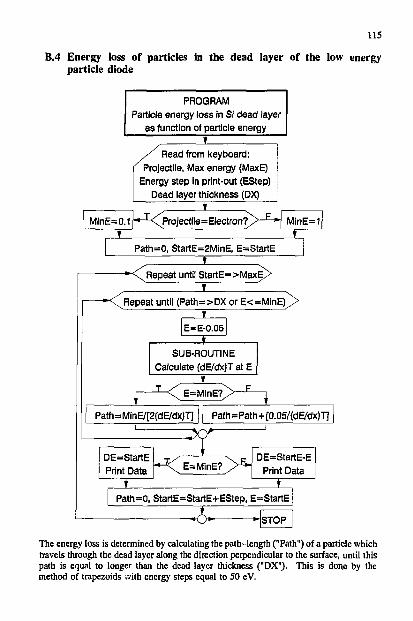
115
B.4 Energy loss of particles in the dead layer of the low energy particle diode
PROGRAM Particle energy loss in SI dead layer
as function of particle energy
/ Read from keyboard: Projectile, Max energy (MaxE)
Energy step in print-out (EStep) Dead layer thickness (DX)
MinE= 0.1 *J<^Pro|ect'te=Electron? X
MinE=1
Path=0, StartE=2MinE, E=StartE
- - < ^ Repeat until StartE=>MaxE>
Repeat until (Path=>DX or E< =MinE)^>
E=E-0.05 X
SUB-ROUTINE Calculate (dE/dx)T at E
r 1—\ E=MinE?^>— E—i
Path=MinE/[2(dE/dx)T] [ Path=Path+[0.05/(dE/dx)T]
X
3: DE=StartE -r/ • v p Print nats K R O M M E T > ^
DE=StartE-E Print Data
X Path=0, StartE=StartE+EStep, E=StartE
-3. STOP
The energy loss is determined by calculating the path-length ("Path") of a particle which travels through the dead layer along the direction perpendicular to the surface, until this path is equal to longer than the dead layer thickness ("DX"). This is done by the method of trapezoids .vith energy steps equal to 50 eV.