devices and communication buses for devices network– spi, sci, si and sdio port/devices for serial...
TRANSCRIPT
DEVICES AND COMMUNICATION
BUSES FOR DEVICES NETWORK–
SPI, SCI, SI and SDIO Port/devices for Serial DataCommunication
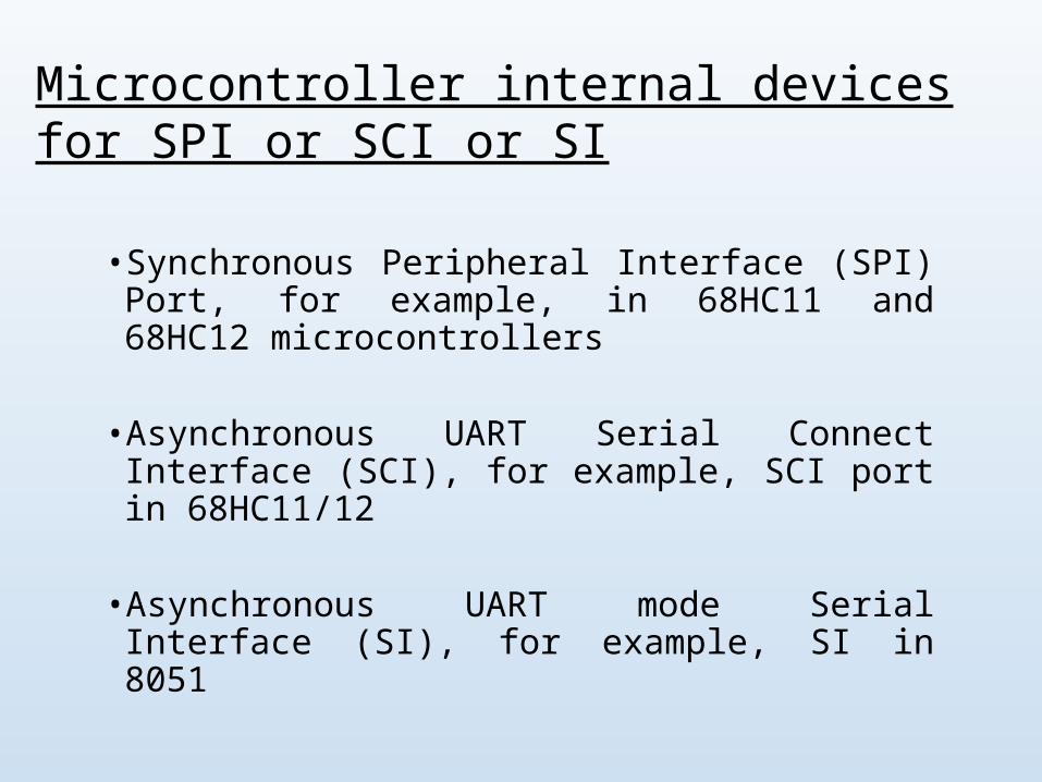
Microcontroller internal devices for SPI or SCI or SI
• Synchronous Peripheral Interface (SPI) Port, for example, in 68HC11 and 68HC12 microcontrollers
• Asynchronous UART Serial Connect Interface (SCI), for example, SCI port in 68HC11/12
• Asynchronous UART mode Serial Interface (SI), for example, SI in 8051

SPI: Synchronous Serial Peripheral Interface
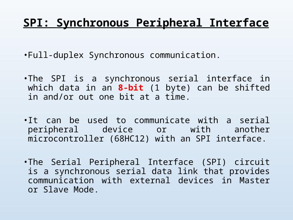
SPI: Synchronous Peripheral Interface
• Full-duplex Synchronous communication.
• The SPI is a synchronous serial interface in which data in an 8-bit (1 byte) can be shifted in and/or out one bit at a time.
• It can be used to communicate with a serial peripheral device or with another microcontroller (68HC12) with an SPI interface.
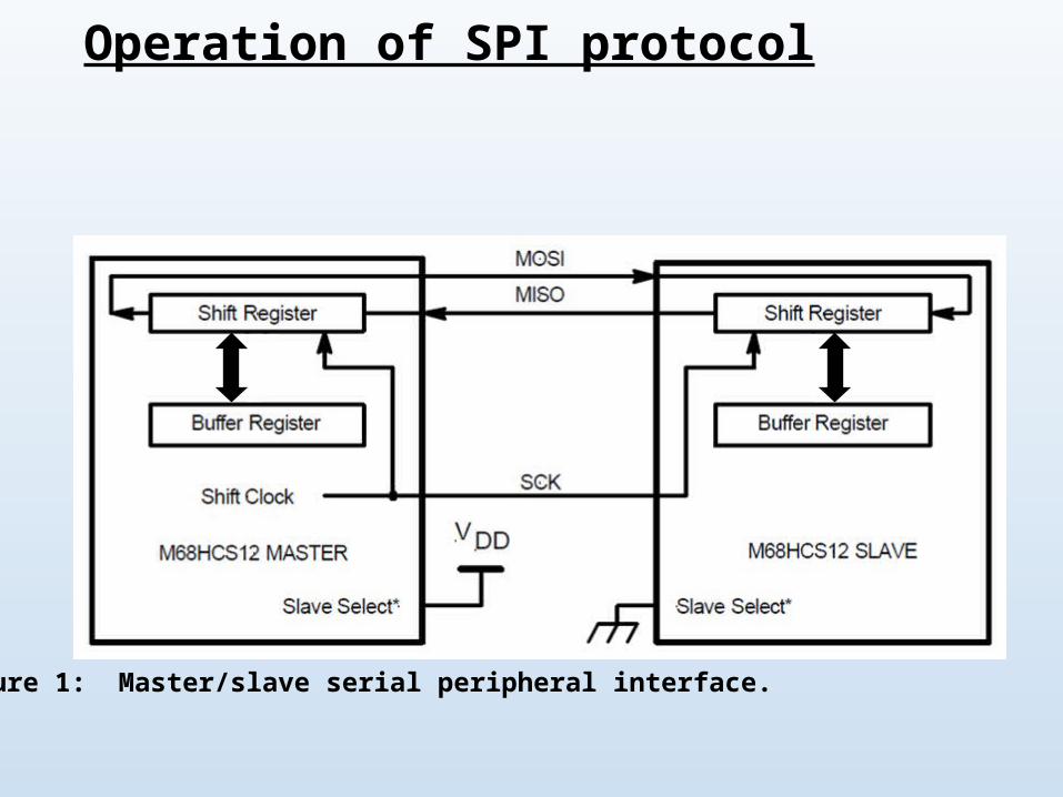
• The Serial Peripheral Interface (SPI) circuit is a synchronous serial data link that provides communication with external devices in Master or Slave Mode.
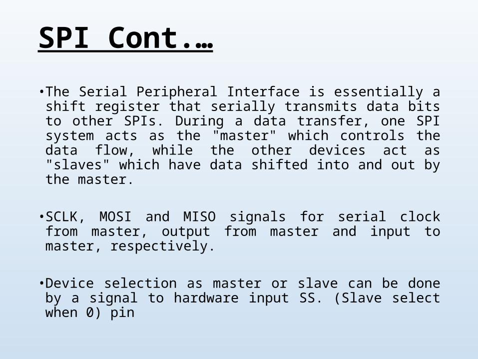
• The Serial Peripheral Interface is essentially a shift register that serially transmits data bits to other SPIs. During a data transfer, one SPI system acts as the "master" which controls the data flow, while the other devices act as "slaves" which have data shifted into and out by the master.
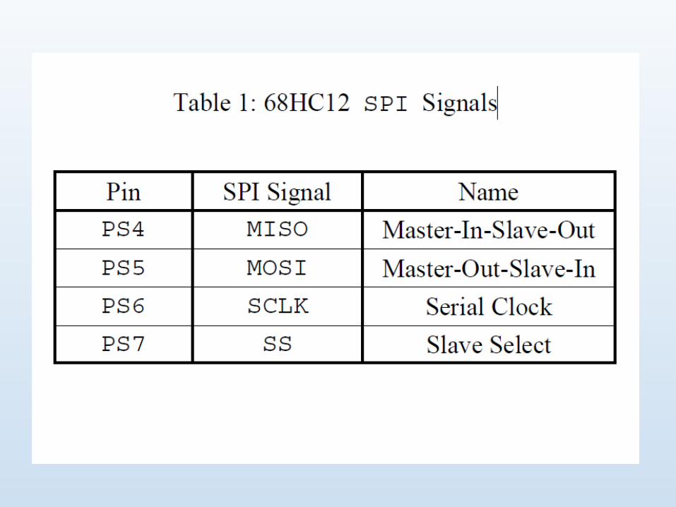
• SCLK, MOSI and MISO signals for serial clock from master, output from master and input to master, respectively.
• Device selection as master or slave can be done by a signal to hardware input SS. (Slave select when 0) pin
SPI Cont.…
Operation of SPI protocol
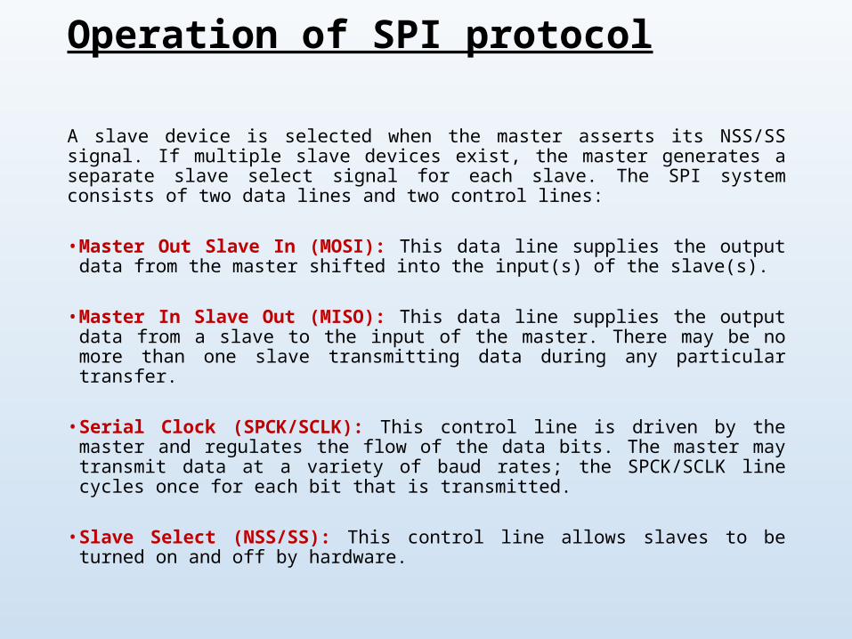
A slave device is selected when the master asserts its NSS/SS signal. If multiple slave devices exist, the master generates a separate slave select signal for each slave. The SPI system consists of two data lines and two control lines:
• Master Out Slave In (MOSI): This data line supplies the output data from the master shifted into the input(s) of the slave(s).
• Master In Slave Out (MISO): This data line supplies the output data from a slave to the input of the master. There may be no more than one slave transmitting data during any particular transfer.
• Serial Clock (SPCK/SCLK): This control line is driven by the master and regulates the flow of the data bits. The master may transmit data at a variety of baud rates; the SPCK/SCLK line cycles once for each bit that is transmitted.
• Slave Select (NSS/SS): This control line allows slaves to be turned on and off by hardware.
Operation of SPI protocol
Figure 1: Master/slave serial peripheral interface.
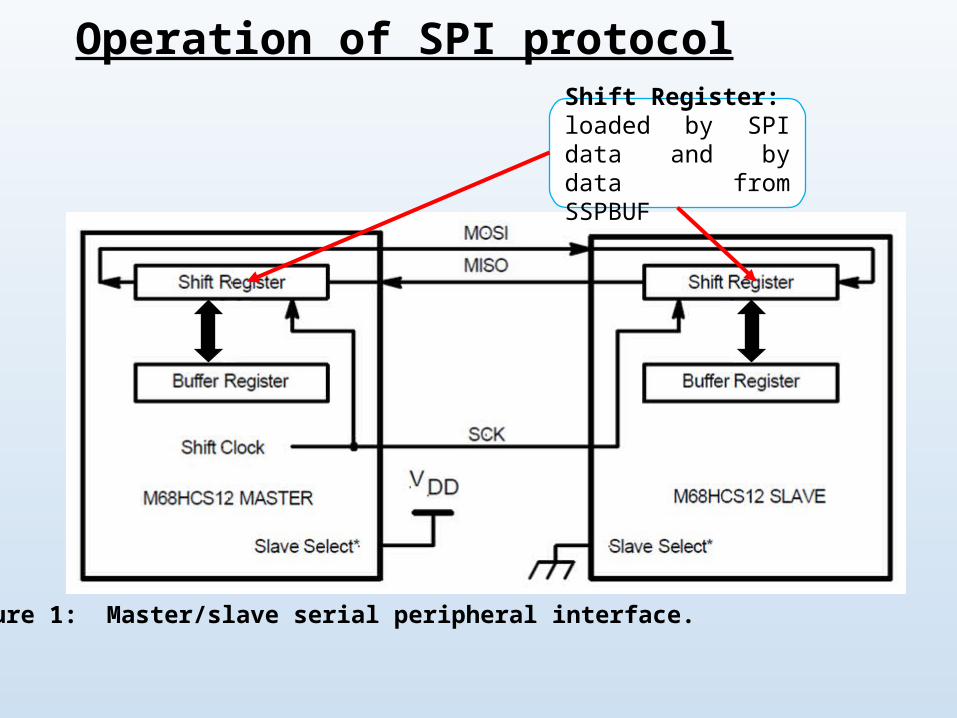
Figure 1: Master/slave serial peripheral interface.
Operation of SPI protocol
Shift Register:loaded by SPI data and by data from SSPBUF
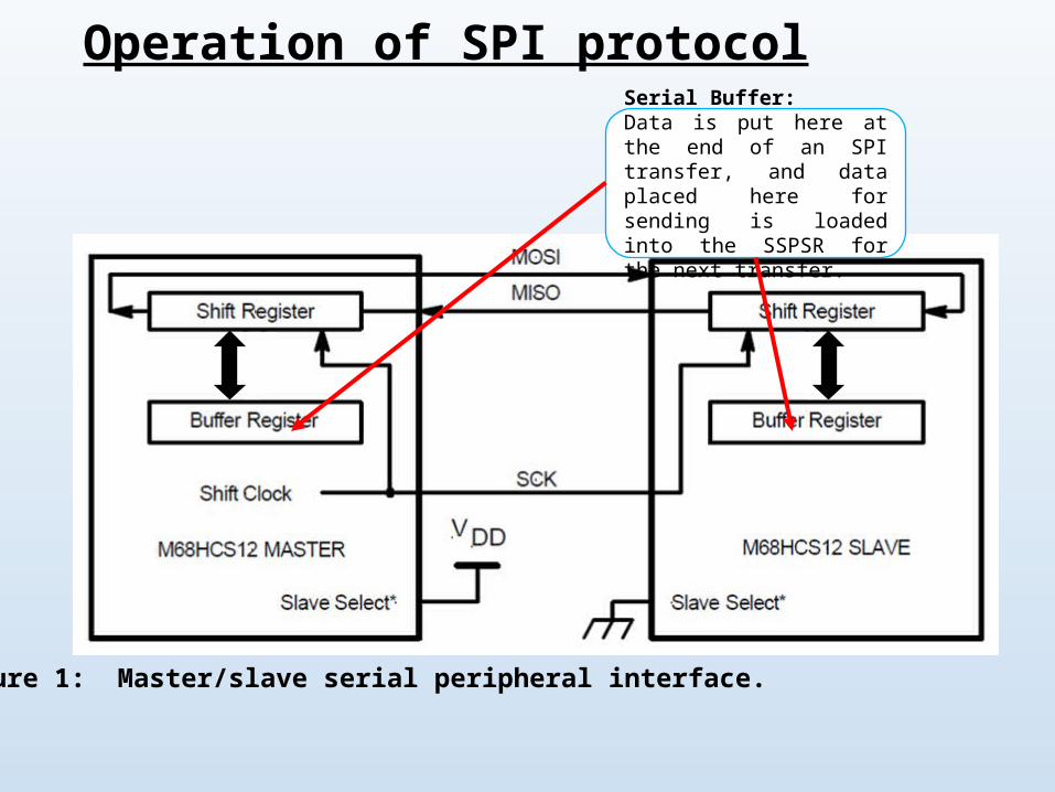
Figure 1: Master/slave serial peripheral interface.
Operation of SPI protocol
Serial Buffer:Data is put here at the end of an SPI transfer, and data placed here for sending is loaded into the SSPSR for the next transfer.
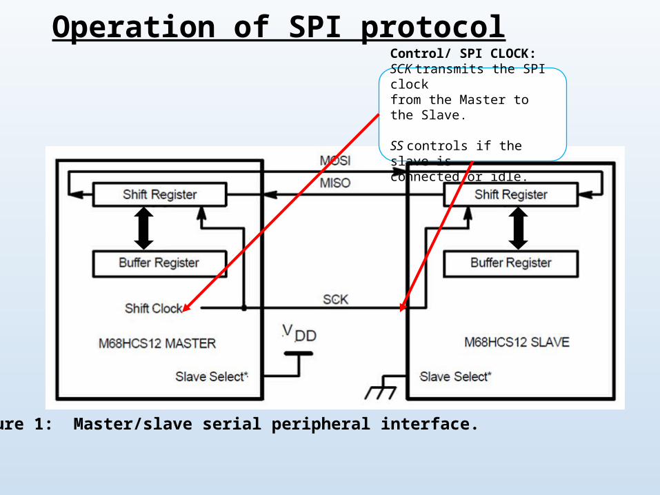
Figure 1: Master/slave serial peripheral interface.
Operation of SPI protocolControl/ SPI CLOCK:SCK transmits the SPI clockfrom the Master to the Slave.
SS controls if the slave isconnected or idle.
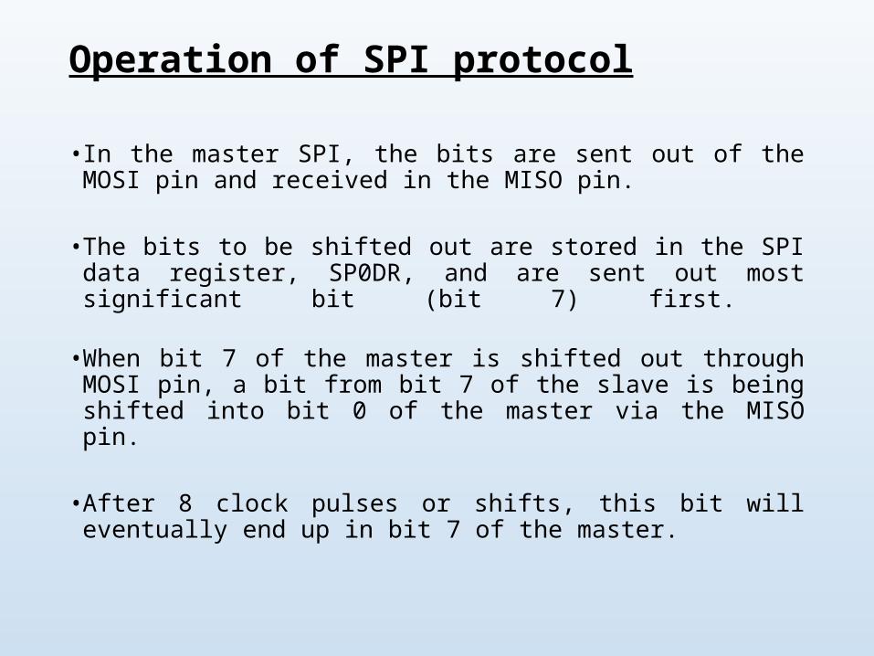
• In the master SPI, the bits are sent out of the MOSI pin and received in the MISO pin.
• The bits to be shifted out are stored in the SPI data register, SP0DR, and are sent out most significant bit (bit 7) first.
•When bit 7 of the master is shifted out through MOSI pin, a bit from bit 7 of the slave is being shifted into bit 0 of the master via the MISO pin.
• After 8 clock pulses or shifts, this bit will eventually end up in bit 7 of the master.
Operation of SPI protocol
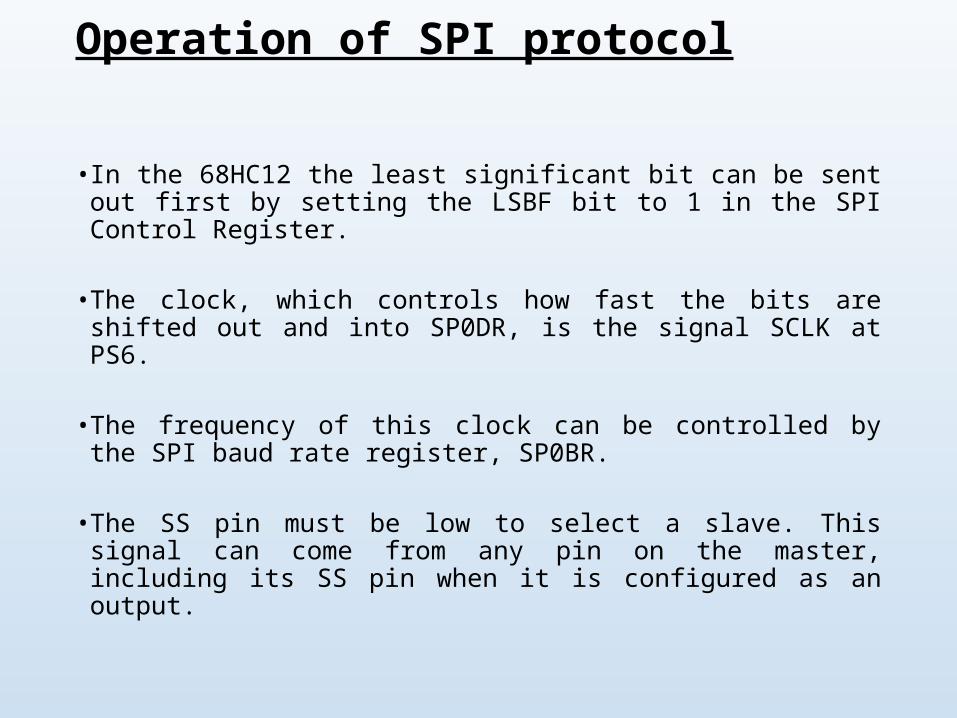
• In the 68HC12 the least significant bit can be sent out first by setting the LSBF bit to 1 in the SPI Control Register.
• The clock, which controls how fast the bits are shifted out and into SP0DR, is the signal SCLK at PS6.
• The frequency of this clock can be controlled by the SPI baud rate register, SP0BR.
• The SS pin must be low to select a slave. This signal can come from any pin on the master, including its SS pin when it is configured as an output.
Operation of SPI protocol
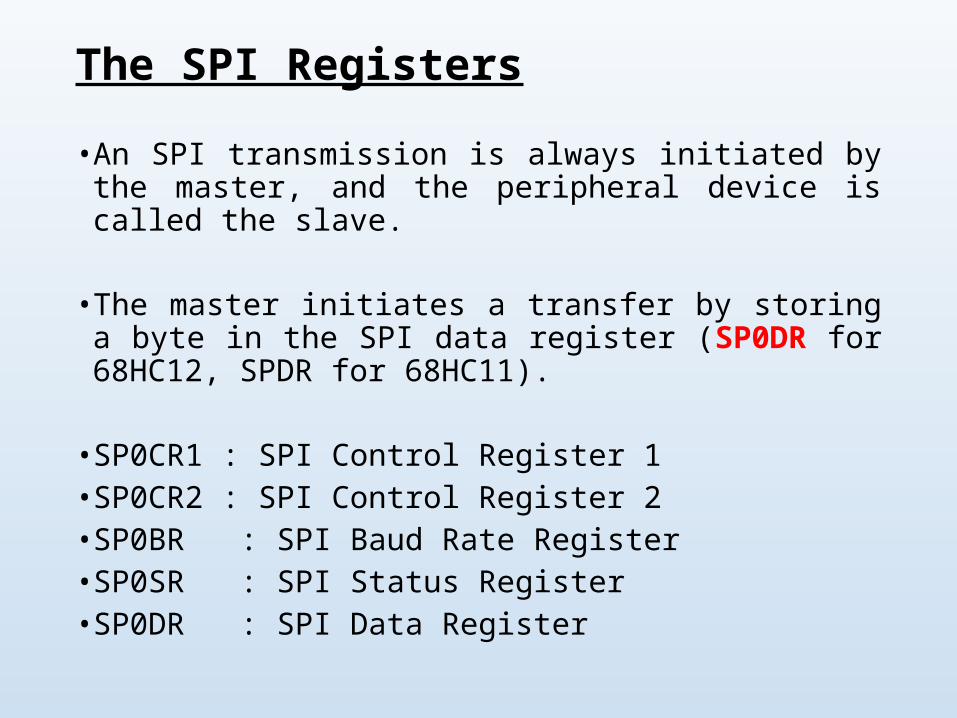
The SPI Registers
• An SPI transmission is always initiated by the master, and the peripheral device is called the slave.
• The master initiates a transfer by storing a byte in the SPI data register (SP0DR for 68HC12, SPDR for 68HC11).
• SP0CR1 : SPI Control Register 1• SP0CR2 : SPI Control Register 2 • SP0BR : SPI Baud Rate Register• SP0SR : SPI Status Register• SP0DR : SPI Data Register
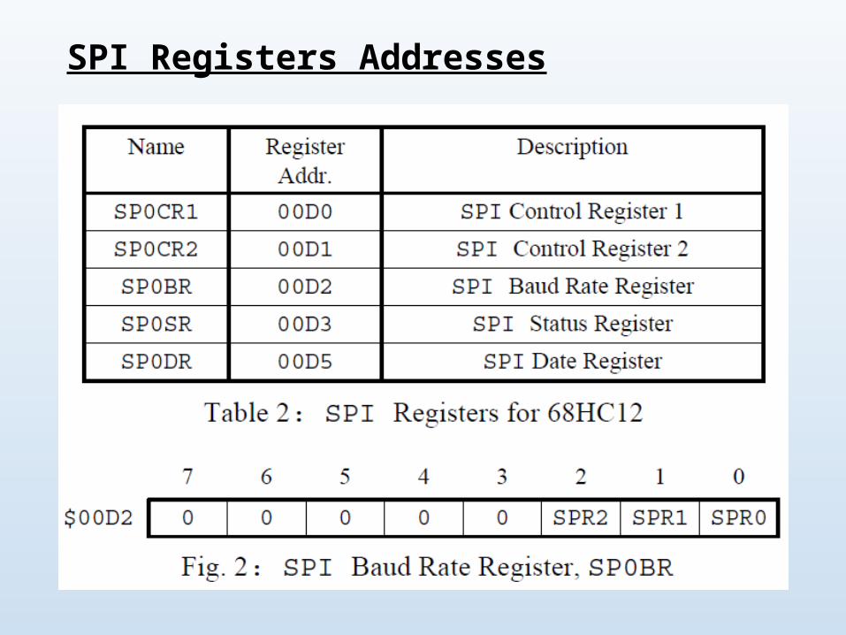
SPI Registers Addresses

Table 2: 68HC12 SPI Clock Rate Selection
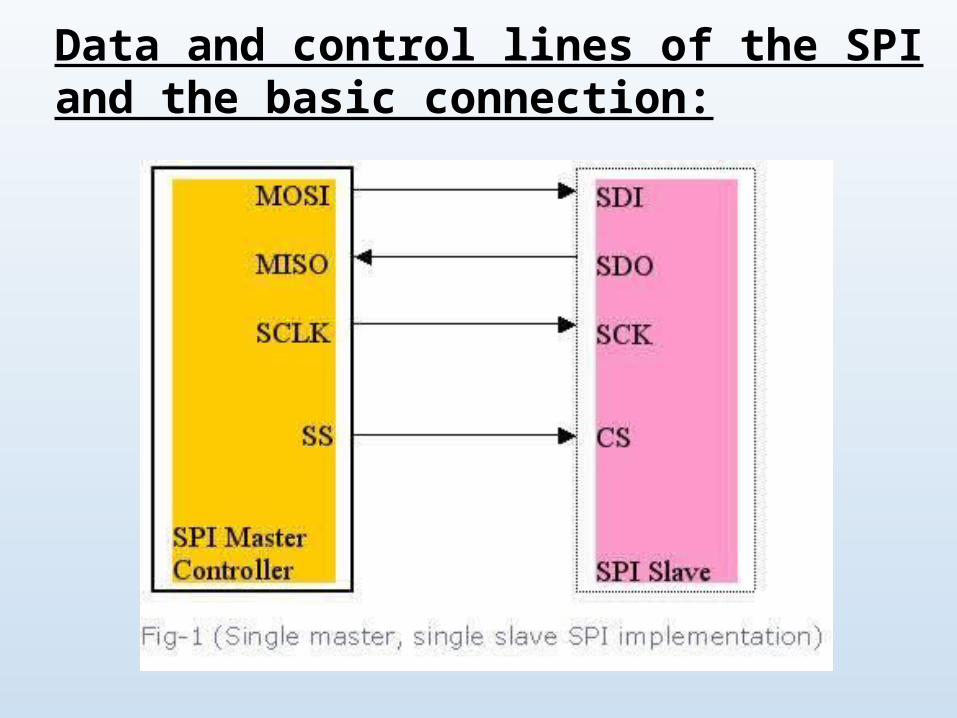
Data and control lines of the SPI and the basic connection:
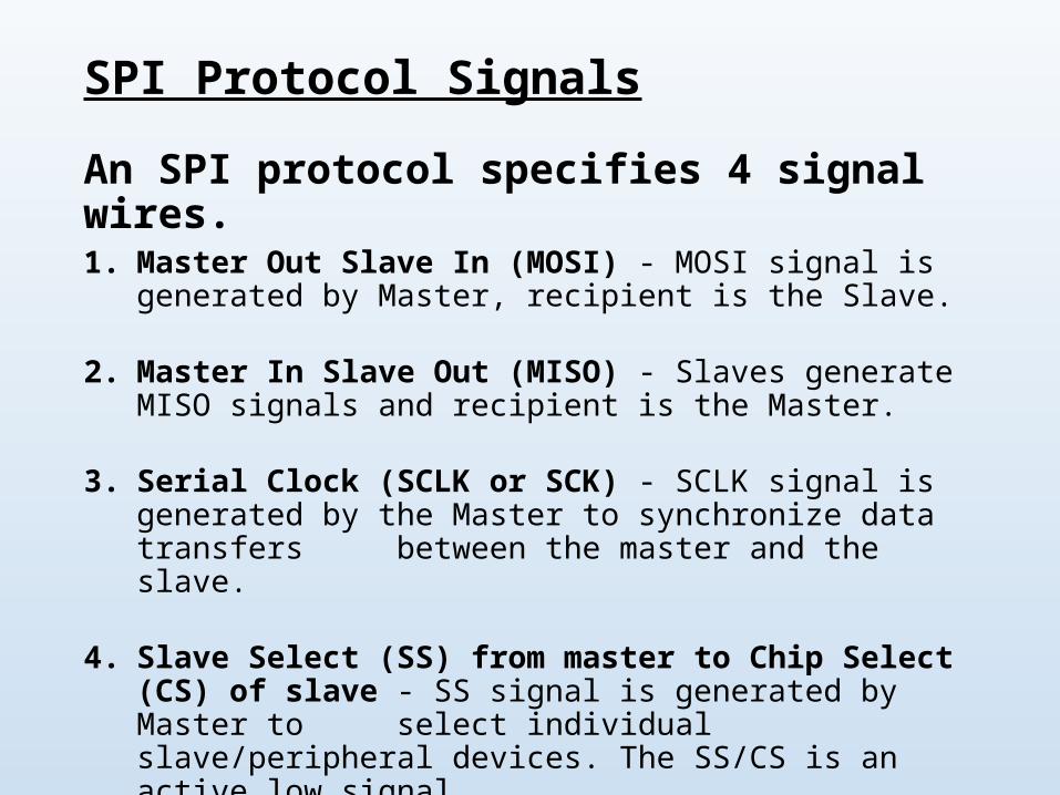
SPI Protocol Signals
An SPI protocol specifies 4 signal wires.1. Master Out Slave In (MOSI) - MOSI signal is generated by Master,
recipient is the Slave.
2. Master In Slave Out (MISO) - Slaves generate MISO signals and recipient is the Master.
3. Serial Clock (SCLK or SCK) - SCLK signal is generated by the Master to synchronize data transfers between the master and the slave.
4. Slave Select (SS) from master to Chip Select (CS) of slave - SS signal is generated by Master to select individual slave/peripheral devices. The SS/CS is an active low signal.
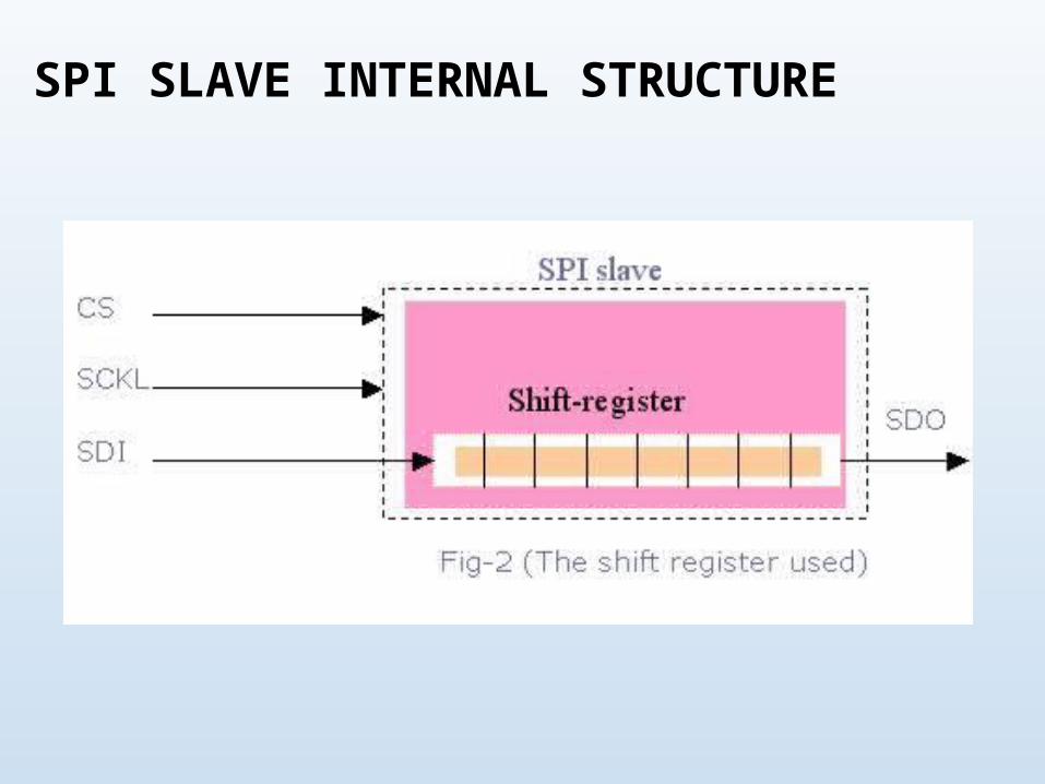
SPI SLAVE INTERNAL STRUCTURE
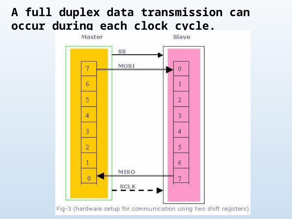
A full duplex data transmission can occur during each clock cycle.
Different types of configurations:• Suppose a master-microcontroller needs to talk to multiple SP
Peripherals. There are 2 ways to set things up:
1. Cascaded slaves or daisy-chained slaves
2. Independent slaves or parallel configuration
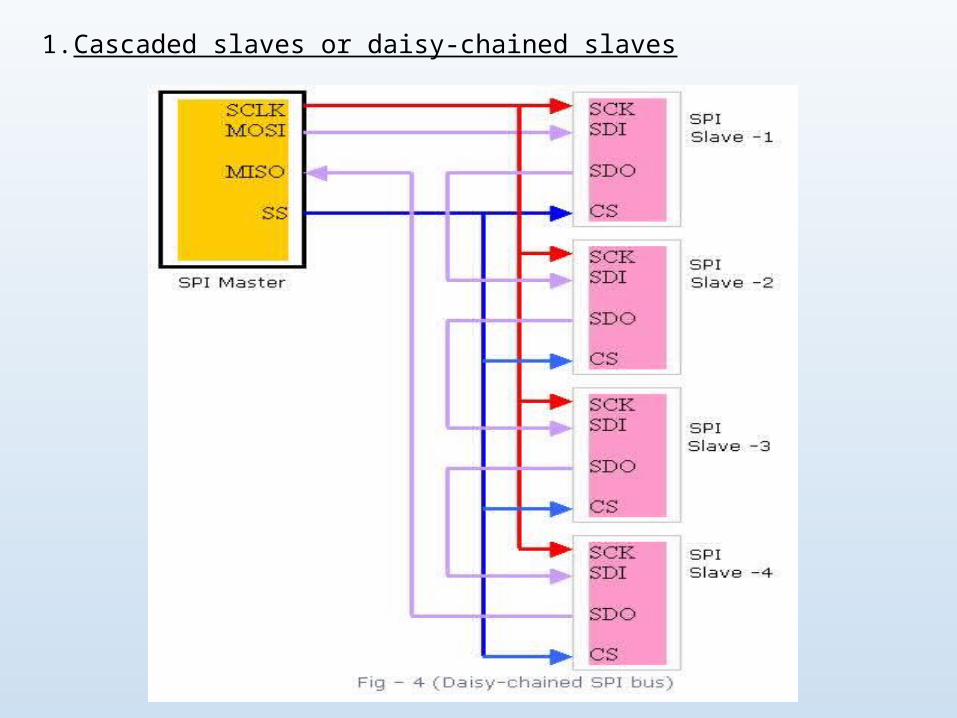
1. Cascaded slaves or daisy-chained slaves
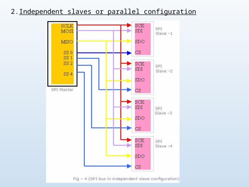
2. Independent slaves or parallel configuration
• 68HC11/12 uses synchronous serial communication (SPI Protocol)
• 68HC12 provides SPI communication device operation at 4Mbps.
• 68HC11 provides SPI communication device operation at 2Mbps.
Examples
Advantages of SPI
1. Full duplex communication2. Higher throughput than I²C protocol 3. Not limited to 8-bit words in the case of bit-transferring 4. Arbitrary choice of message size, contents, and purpose 5. Simple hardware interfacing 6. Typically lower power requirements than I²C due to less circuitry.7. No arbitration or associated failure modes. 8. Slaves use the master's clock, and don't need precision oscillators. 9. Transceivers are not needed.
At most one "unique" bus signal per device (CS); all others are shared
Disadvantages of SPI
1. Requires more pins on IC packages than I²C.2. No in-band addressing. Out-of-band chip select signals are
required on shared busses.3. No hardware flow control4. Multi-master busses are rare and awkward, and are usually limited
to a single slave. 5. Only handles short distances compared to RS-232 & CAN.

SCI: Serial Connect Interface Port
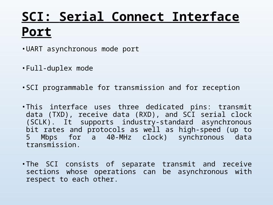
SCI: Serial Connect Interface Port• UART asynchronous mode port
• Full-duplex mode
• SCI programmable for transmission and for reception
• This interface uses three dedicated pins: transmit data (TXD), receive data (RXD), and SCI serial clock (SCLK). It supports industry-standard asynchronous bit rates and protocols as well as high-speed (up to 5 Mbps for a 40-MHz clock) synchronous data transmission.
• The SCI consists of separate transmit and receive sections whose operations can be asynchronous with respect to each other.
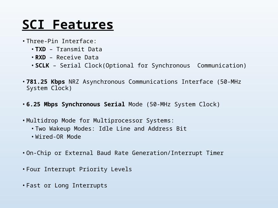
• Three-Pin Interface:• TXD – Transmit Data• RXD – Receive Data• SCLK – Serial Clock(Optional for Synchronous Communication)
• 781.25 Kbps NRZ Asynchronous Communications Interface (50-MHz System Clock)
• 6.25 Mbps Synchronous Serial Mode (50-MHz System Clock)
• Multidrop Mode for Multiprocessor Systems:• Two Wakeup Modes: Idle Line and Address Bit• Wired-OR Mode
• On-Chip or External Baud Rate Generation/Interrupt Timer
• Four Interrupt Priority Levels
• Fast or Long Interrupts
SCI Features
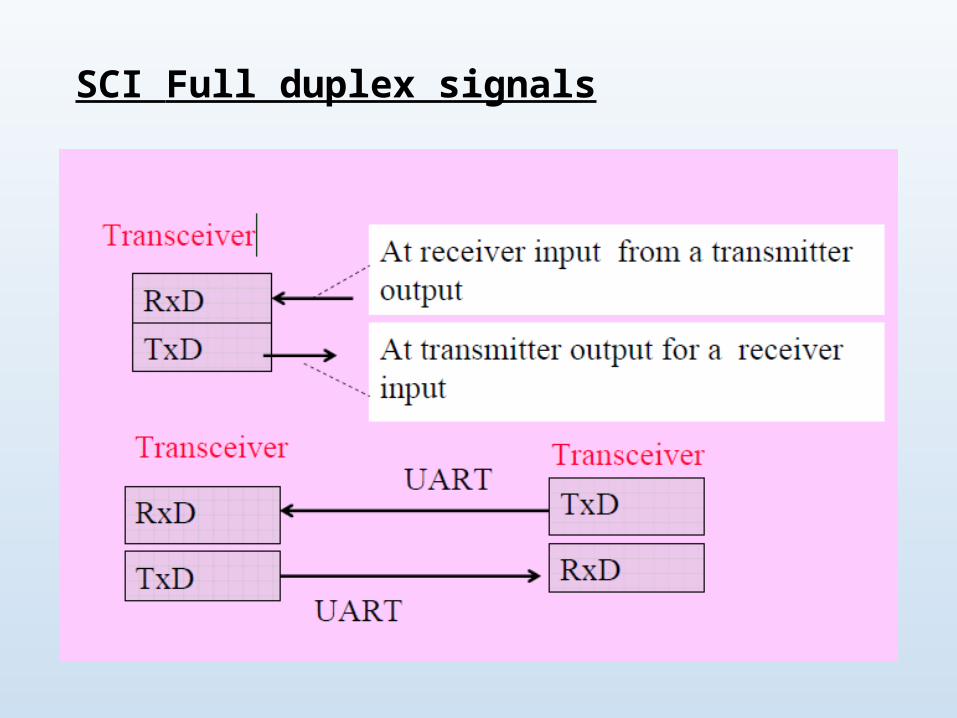
SCI Full duplex signals
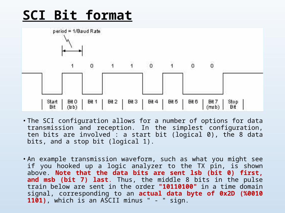
SCI Bit format
• The SCI configuration allows for a number of options for data transmission and reception. In the simplest configuration, ten bits are involved : a start bit (logical 0), the 8 data bits, and a stop bit (logical 1).
• An example transmission waveform, such as what you might see if you hooked up a logic analyzer to the TX pin, is shown above. Note that the data bits are sent lsb (bit 0) first, and msb (bit 7) last. Thus, the middle 8 bits in the pulse train below are sent in the order "10110100" in a time domain signal, corresponding to an actual data byte of 0x2D (%0010 1101), which is an ASCII minus " - " sign.

• The data rate out of/into the SCI is determined by the baud rate, and is an essential value to consider in any SCI setup.
• For our Dragon 12 running with a PLL controlled clock at 24 MHz, the baud rate is determined by the following formula:
• where BR is the content of the SCI1BDH/L Baud Rate Registers at addresses $00D0 and $00D1. For example, for a baud rate of 9600 (baud period ~ 100 usec) , we want a BR of about 156 = 9CH, so we write 00H to SCI1BDH and 9CH to SCI1BDL.
• Note that the baud rate is the same for transmission and reception for a given SCI port; we can't set one baud rate for transmission, and another for reception on a given port.
SCI BAUD rate = 24,000,000/(16 x BR)
SCI Bit format cont.….
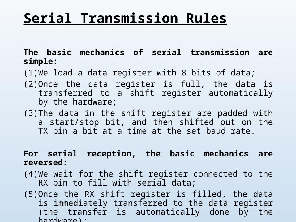
Serial Transmission Rules
The basic mechanics of serial transmission are simple: (1) We load a data register with 8 bits of data; (2) Once the data register is full, the data is transferred to a shift register
automatically by the hardware; (3) The data in the shift register are padded with a start/stop bit, and
then shifted out on the TX pin a bit at a time at the set baud rate.
For serial reception, the basic mechanics are reversed: (4) We wait for the shift register connected to the RX pin to fill with serial
data; (5) Once the RX shift register is filled, the data is immediately transferred
to the data register (the transfer is automatically done by the hardware);
(6) We then read the data register to see what data was received.
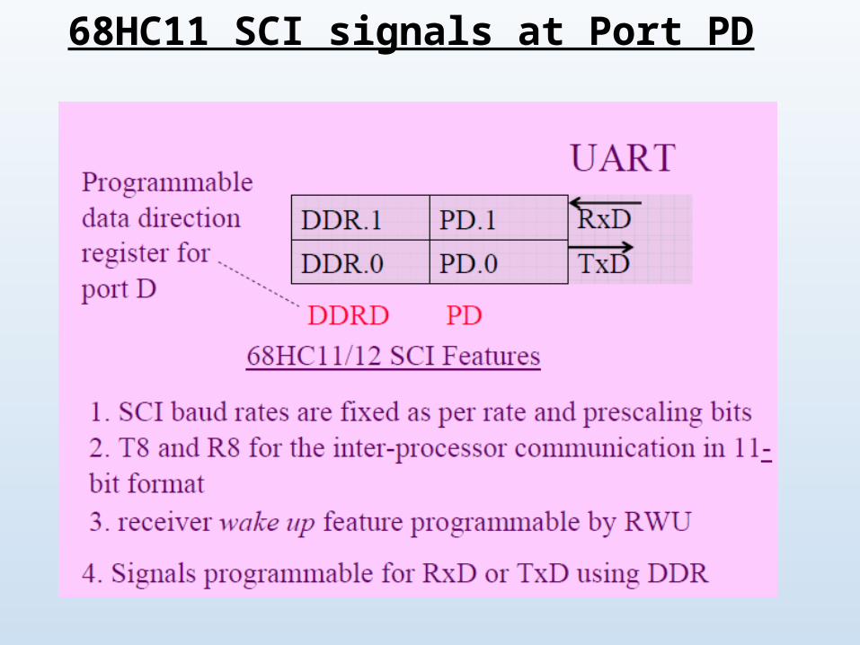
68HC11 SCI signals at Port PD
SI: Serial Interface Port

Serial Interface (SI) Port
• UART 10T or 11T mode asynchronous port interface.
• Functions as USRT (universal synchronous receiver and transmitter) also.
• SI is therefore synchronous-asynchronous serial communication port called USART (universal synchronous-asynchronous receiver and transmitter) port.
• SI is an internal serial IO device in 8051.
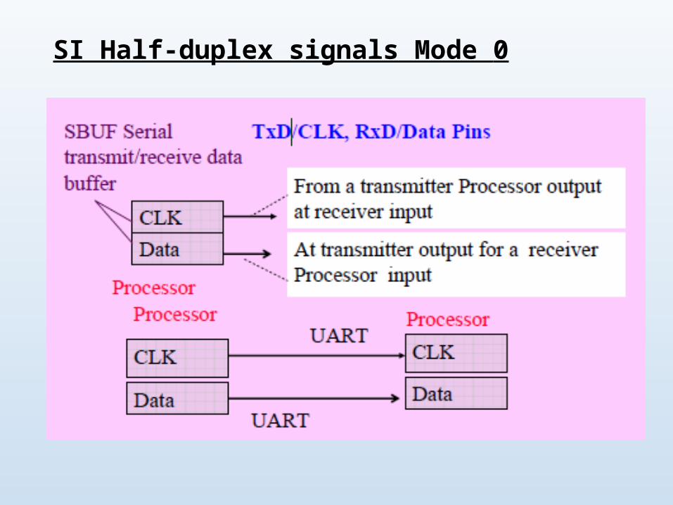
SI Half-duplex signals Mode 0
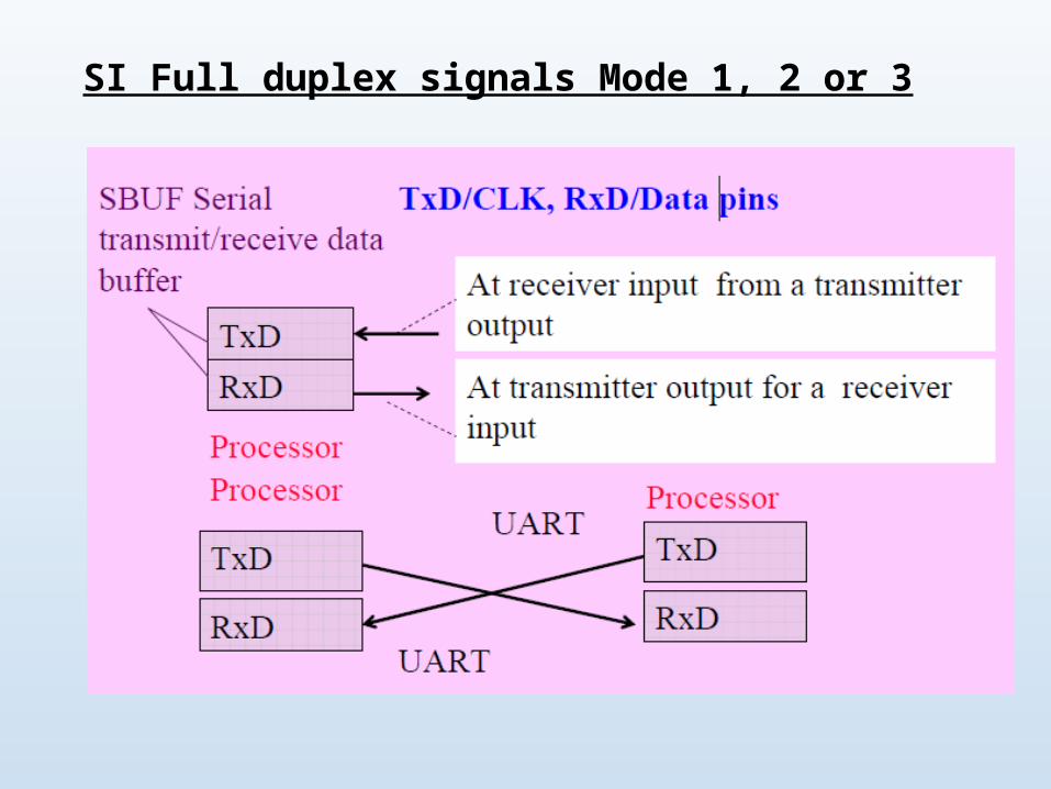
SI Full duplex signals Mode 1, 2 or 3
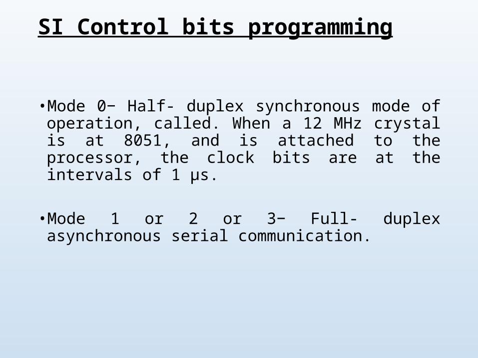
SI Control bits programming
•Mode 0− Half- duplex synchronous mode of operation, called. When a 12 MHz crystal is at 8051, and is attached to the processor, the clock bits are at the intervals of 1 μs.
•Mode 1 or 2 or 3− Full- duplex asynchronous serial communication.
SDIO: Secure Digital Input Output
Secure Digital Association (SD)
• SD− an association of over 700 companies started from 3 companies in 1999
• Created a new flash memory card format, called SD format for IOs.
• SDIO card has become popular feature in handheld mobile devices, PDAs, digital cameras and embedded systems.
• SD card size− just 0.14 cm × 2.4 cm × 3.2 cm.
• Allowed to stick out of the handheld device open slot, which can be at the top in order to facilitate insertion of the SD card

• A processing element functions used SDIO host controller to process the IOs.
• Controller may include SPI controller to support SPI mode for the IOs and also supports the needed protocol functionality internally
SDIO card host controller
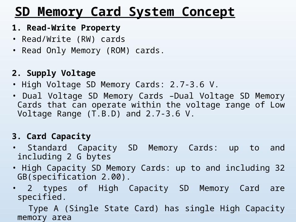
1. Read-Write Property• Read/Write (RW) cards• Read Only Memory (ROM) cards.
2. Supply Voltage• High Voltage SD Memory Cards: 2.7-3.6 V.• Dual Voltage SD Memory Cards –Dual Voltage SD Memory Cards that can
operate within the voltage range of Low Voltage Range (T.B.D) and 2.7-3.6 V.
3. Card Capacity• Standard Capacity SD Memory Cards: up to and including 2 G bytes• High Capacity SD Memory Cards: up to and including 32 GB(specification 2.00).• 2 types of High Capacity SD Memory Card are specified. Type A (Single State Card) has single High Capacity memory area Type B (Dual State Card) has both High Capacity memory area and Standard
Capacity memory area. In Type B card, only one memory area can be used at any given time.
SD Memory Card System Concept

4. Speed ClassFour Speed Classes are defined and indicate minimum performance of the cards• Class 0 - These class cards do not specify performance. It includes all the legacy
cards prior to specification 2.00, regardless of its performance• Class 2 - Are more than or equal to 2 MB/sec performance.• Class 4 - Are more than or equal to 4 MB/sec performance.• Class 6 - Are more than or equal to 6 MB/sec performance.
5. Bus TopologyThe SD bus includes the following 9 signals:• CLK : Host to card clock signal• CMD : Bidirectional Command/Response signal• DAT 0 - DAT 3 : 4 Bidirectional data signals.• VDD , VSS1 , VSS2 : Power and ground signals.
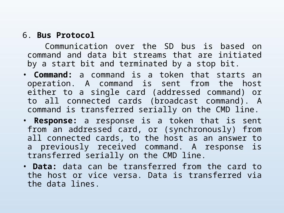
6. Bus Protocol Communication over the SD bus is based on command and data
bit streams that are initiated by a start bit and terminated by a stop bit.
• Command: a command is a token that starts an operation. A command is sent from the host either to a single card (addressed command) or to all connected cards (broadcast command). A command is transferred serially on the CMD line.
• Response: a response is a token that is sent from an addressed card, or (synchronously) from all connected cards, to the host as an answer to a previously received command. A response is transferred serially on the CMD line.
• Data: data can be transferred from the card to the host or vice versa. Data is transferred via the data lines.

SDIO Signals Description
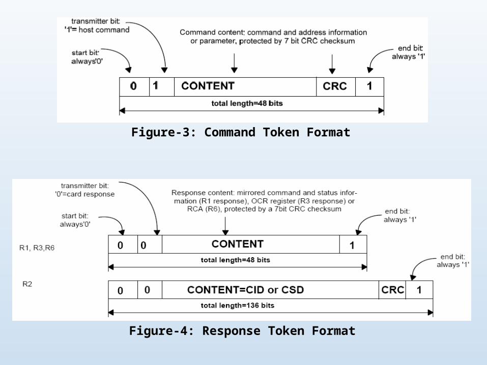
Figure-3: Command Token Format
Figure-4: Response Token Format
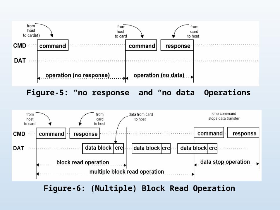
Figure-5: “no response” and “no data” Operations
Figure-6: (Multiple) Block Read Operation
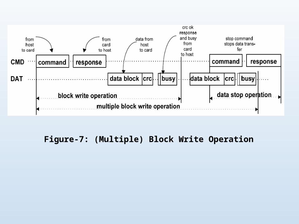
Figure-7: (Multiple) Block Write Operation
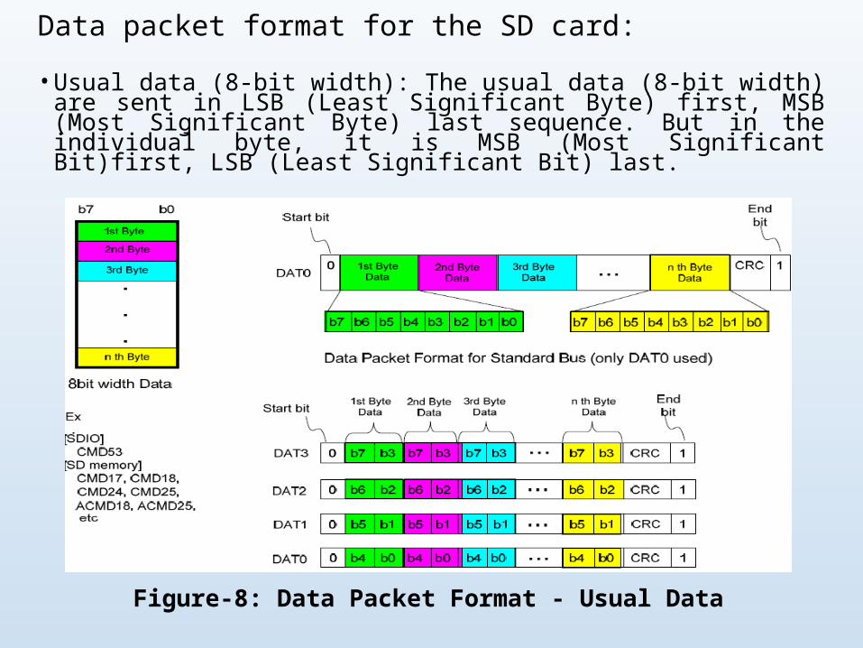
Figure-8: Data Packet Format - Usual Data
Data packet format for the SD card:
• Usual data (8-bit width): The usual data (8-bit width) are sent in LSB (Least Significant Byte) first, MSB (Most Significant Byte) last sequence. But in the individual byte, it is MSB (Most Significant Bit)first, LSB (Least Significant Bit) last.
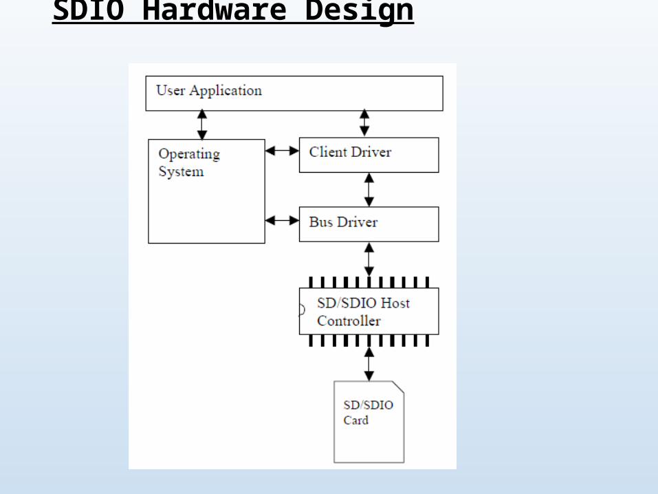
SDIO Hardware Design
DEVICES AND COMMUNICATIONBUSES FOR DEVICES
NETWORK–
Parallel port at devices
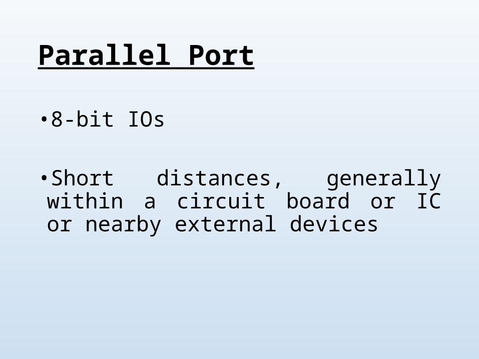
Parallel Port
•8-bit IOs
•Short distances, generally within a circuit board or IC or nearby external devices
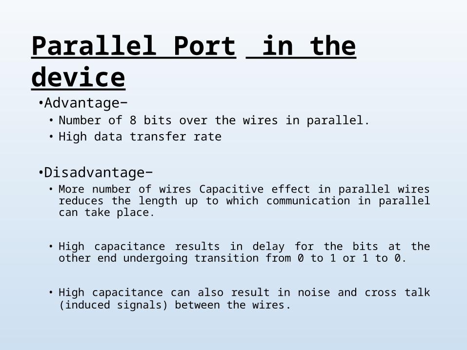
• Advantage− • Number of 8 bits over the wires in parallel.• High data transfer rate
• Disadvantage− • More number of wires Capacitive effect in parallel wires reduces the
length up to which communication in parallel can take place.
• High capacitance results in delay for the bits at the other end undergoing transition from 0 to 1 or 1 to 0.
• High capacitance can also result in noise and cross talk (induced signals) between the wires.
Parallel Port in the device
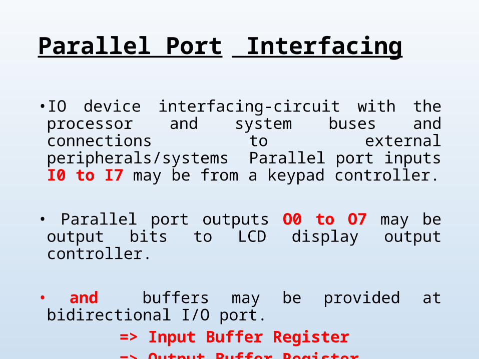
• IO device interfacing-circuit with the processor and system buses and connections to external peripherals/systems Parallel port inputs I0 to I7 may be from a keypad controller.
• Parallel port outputs O0 to O7 may be output bits to LCD display output controller.
• and buffers may be provided at bidirectional I/O port. => Input Buffer Register => Output Buffer Register
Parallel Port Interfacing
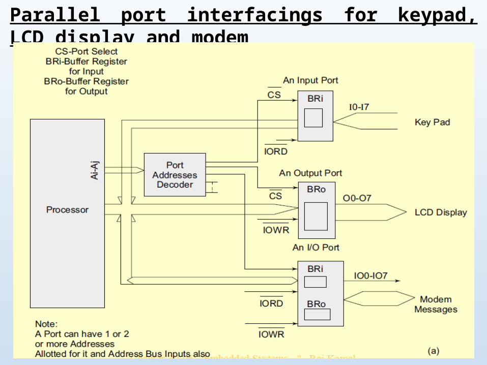
Parallel port interfacings for keypad, LCD display and modem
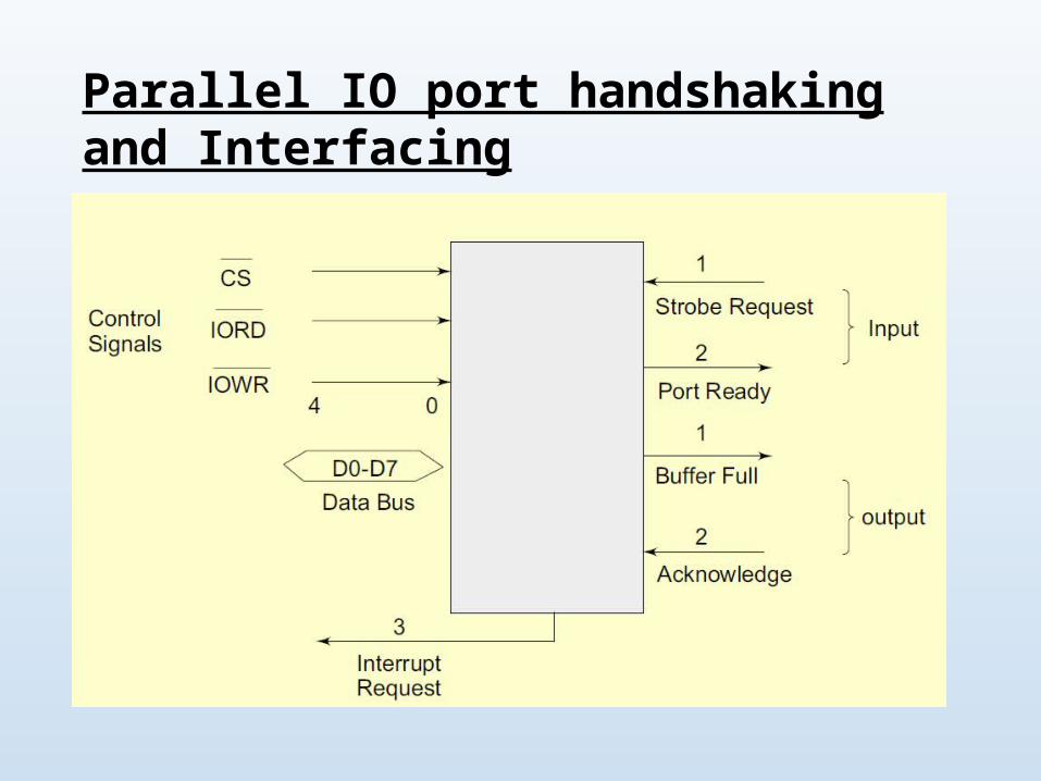
Parallel IO port handshaking and Interfacing
Handshaking signals to and from an externalperipheral device for input at port• Device makes a strobe request to port, STROBE after it is
ready to send the byte and
• System I/O port sends the acknowledgement, PORT READY.
• System I/O port receives data in buffer and then issues an interrupt signal, INT to processor to enable an ISR execution
• Device sends the message ACKNOWLEDGE when and the I/O device port ends the BUFFER FULL signal to inform that the is buffer full.
• The processor is sent the INTERRUPT REQUEST message, when the transmitting-buffer is empty (available for next write)
Handshaking signals to and from an externalperipheral device for Output at port
Port Interrupt to processor
•When receiving-buffer is full (available for next read)
• When transmitting-buffer is empty (available for next write)
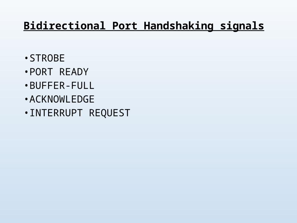
Bidirectional Port Handshaking signals
• STROBE• PORT READY• BUFFER-FULL• ACKNOWLEDGE• INTERRUPT REQUEST
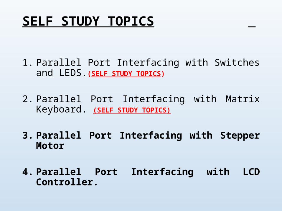
SELF STUDY TOPICS
1. Parallel Port Interfacing with Switches and LEDS.(SELF STUDY TOPICS)
2. Parallel Port Interfacing with Matrix Keyboard. (SELF STUDY TOPICS)
3. Parallel Port Interfacing with Stepper Motor
4. Parallel Port Interfacing with LCD Controller.