drv5023-q1 automotive digital-switch hall effect sensor ... · fa, aj, and bi versions out b rp b...
TRANSCRIPT

FA, AJ, and BI Versions
OUT
BOPBRP BOF
Bhys
B (mT)
FI Version
OUT
BOPBRP BOF
Bhys
B (mT)
Product
Folder
Order
Now
Technical
Documents
Tools &
Software
Support &Community
An IMPORTANT NOTICE at the end of this data sheet addresses availability, warranty, changes, use in safety-critical applications,intellectual property matters and other important disclaimers. PRODUCTION DATA.
DRV5023-Q1SLIS163G –DECEMBER 2014–REVISED MARCH 2017
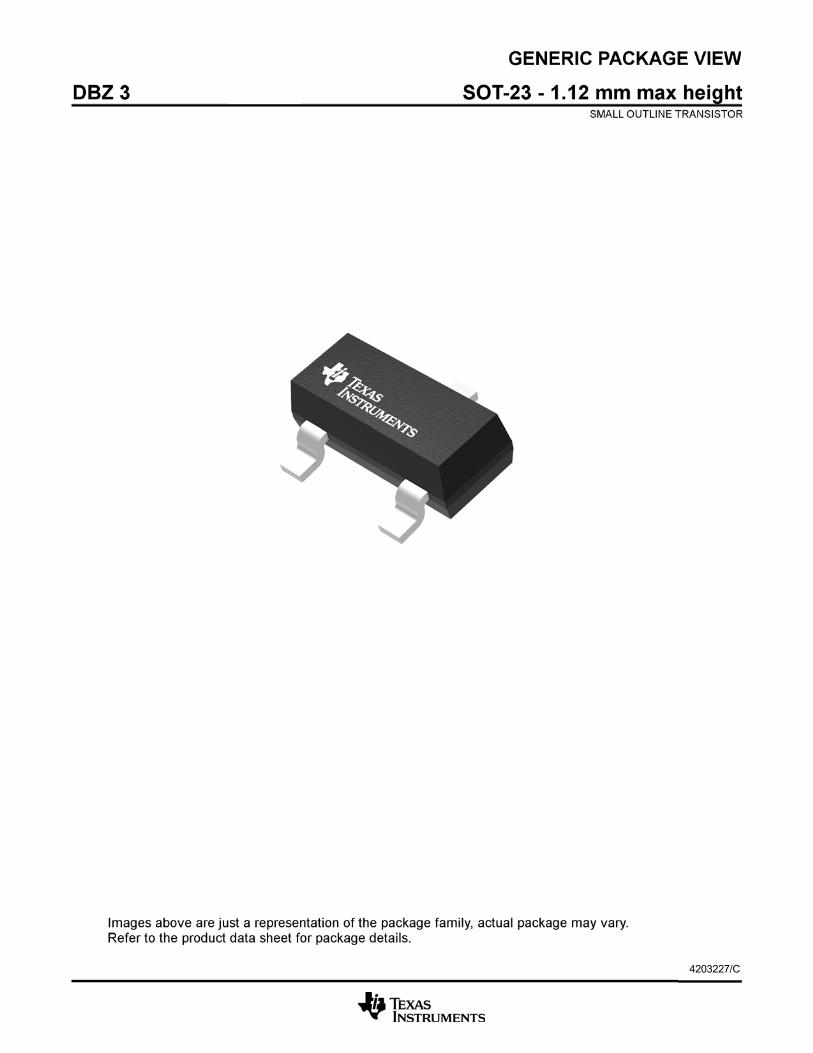
DRV5023-Q1 Automotive Digital-Switch Hall Effect Sensor
1
1 Features1• Digital Unipolar-Switch Hall Sensor• AEC-Q100 Qualified for Automotive Applications
– Grade 1: TA = –40 to 125°C (Q, See DeviceNomenclature)
– Grade 0: TA = –40 to 150°C (E, See DeviceNomenclature)
• Inverse Output Option (FI)• Superior Temperature Stability
– Sensitivity ±10% Over Temperature• Multiple Sensitivity Options (BOP / BRP):
– 3.5 / 2 mT (FA, FI, see Device Nomenclature)– 6.9 / 3.2 mT (AJ, see Device Nomenclature)– 14.5 / 6 mT (BI, see Device Nomenclature)
• Supports a Wide Voltage Range– 2.7 to 38 V– No External Regulator Required
• Open Drain Output (30-mA Sink)• Fast 35-µs Power-On Time• Small Package and Footprint
– Surface Mount 3-Pin SOT-23 (DBZ)– 2.92 mm × 2.37 mm
– Through-Hole 3-Pin TO-92 (LPG)– 4.00 mm × 3.15 mm
• Protection Features– Reverse Supply Protection (up to –22 V)– Supports up to 40-V Load Dump– Output Short-Circuit Protection– Output Current Limitation– OUT Short to Battery Protection
2 Applications• Docking Detection• Door Open and Close Detection• Proximity Sensing• Valve Positioning• Pulse Counting
3 DescriptionThe DRV5023-Q1 device is a chopper-stabilized HallEffect Sensor that offers a magnetic sensing solutionwith superior sensitivity stability over temperature andintegrated protection features.
When the applied magnetic flux density exceeds theBOP threshold, the DRV5023-Q1 open-drain outputgoes low. The output stays low until the fielddecreases to less than BRP, and then the output goesto high impedance. The output current sink capabilityis 30 mA. A wide operating voltage range from 2.7 to38 V with reverse polarity protection up to –22 Vmakes the device suitable for a wide range ofautomotive applications.
Internal protection functions are provided for reversesupply conditions, load dump, and output short circuitor over current.
Device Information(1)
PART NUMBER PACKAGE BODY SIZE (NOM)
DRV5023-Q1SOT-23 (3) 2.92 mm × 1.30 mmTO-92 (3) 4.00 mm × 3.15 mm
(1) For all available packages, see the orderable addendum atthe end of the data sheet.
Output State Device Packages
2
DRV5023-Q1SLIS163G –DECEMBER 2014–REVISED MARCH 2017 www.ti.com
Product Folder Links: DRV5023-Q1
Submit Documentation Feedback Copyright © 2014–2017, Texas Instruments Incorporated
Table of Contents1 Features .................................................................. 12 Applications ........................................................... 13 Description ............................................................. 14 Revision History..................................................... 25 Pin Configuration and Functions ......................... 46 Specifications......................................................... 5
6.1 Absolute Maximum Ratings ...................................... 56.2 ESD Ratings.............................................................. 56.3 Recommended Operating Conditions....................... 56.4 Thermal Information .................................................. 56.5 Electrical Characteristics........................................... 66.6 Switching Characteristics .......................................... 66.7 Magnetic Characteristics........................................... 66.8 Typical Characteristics .............................................. 7
7 Detailed Description .............................................. 97.1 Overview ................................................................... 97.2 Functional Block Diagram ......................................... 97.3 Feature Description................................................. 10
7.4 Device Functional Modes........................................ 158 Application and Implementation ........................ 16
8.1 Application Information............................................ 168.2 Typical Applications ................................................ 16
9 Power Supply Recommendations ...................... 1810 Layout................................................................... 19
10.1 Layout Guidelines ................................................. 1910.2 Layout Example .................................................... 19
11 Device and Documentation Support ................. 2011.1 Device Support...................................................... 2011.2 Documentation Support ........................................ 2111.3 Receiving Notification of Documentation Updates 2111.4 Community Resources.......................................... 2111.5 Trademarks ........................................................... 2111.6 Electrostatic Discharge Caution............................ 2111.7 Glossary ................................................................ 21
12 Mechanical, Packaging, and OrderableInformation ........................................................... 21
4 Revision HistoryNOTE: Page numbers for previous revisions may differ from page numbers in the current version.
Changes from Revision F (September 2016) to Revision G Page
• Added the output jitter parameter to the Switching Characteristics table............................................................................... 6• Added the Output Jitter Characteristic section ..................................................................................................................... 15
Changes from Revision E (August 2016) to Revision F Page
• Made changes to the Power-on time in the Electrical Characteristics table ......................................................................... 6
Changes from Revision D (May 2016) to Revision E Page
• Clarified the output description for the FI device version in the Device Output section ...................................................... 10• Added the Layout section .................................................................................................................................................... 19• Added the Receiving Notification of Documentation Updates section ................................................................................ 21
Changes from Revision C (February 2016) to Revision D Page
• Revised preliminary limits for the FA version ......................................................................................................................... 6
Changes from Revision B (December 2015) to Revision C Page
• Added the FA and FI device options ..................................................................................................................................... 1• Added the typical bandwidth value to the Magnetic Characteristics table ............................................................................ 6

3
DRV5023-Q1www.ti.com SLIS163G –DECEMBER 2014–REVISED MARCH 2017
Product Folder Links: DRV5023-Q1
Submit Documentation FeedbackCopyright © 2014–2017, Texas Instruments Incorporated
Changes from Revision A (May 2015) to Revision B Page
• Corrected body size of SOT-23 package and SIP package name to TO-92 ........................................................................ 1• Added BMAX to Absolute Maximum Ratings ........................................................................................................................... 5• Removed table notes regarding testing for the operating junction temperature in Absolute Maximum Ratings .................. 5• Updated package tape and reel options for M and blank ................................................................................................... 20• Added Community Resources ............................................................................................................................................. 21
Changes from Original (December 2014) to Revision A Page
• Updated device status to production data ............................................................................................................................. 1
1 2 3
VCC
GND
OUT
3
2
GND
OUT
1 VCC
4
DRV5023-Q1SLIS163G –DECEMBER 2014–REVISED MARCH 2017 www.ti.com
Product Folder Links: DRV5023-Q1
Submit Documentation Feedback Copyright © 2014–2017, Texas Instruments Incorporated
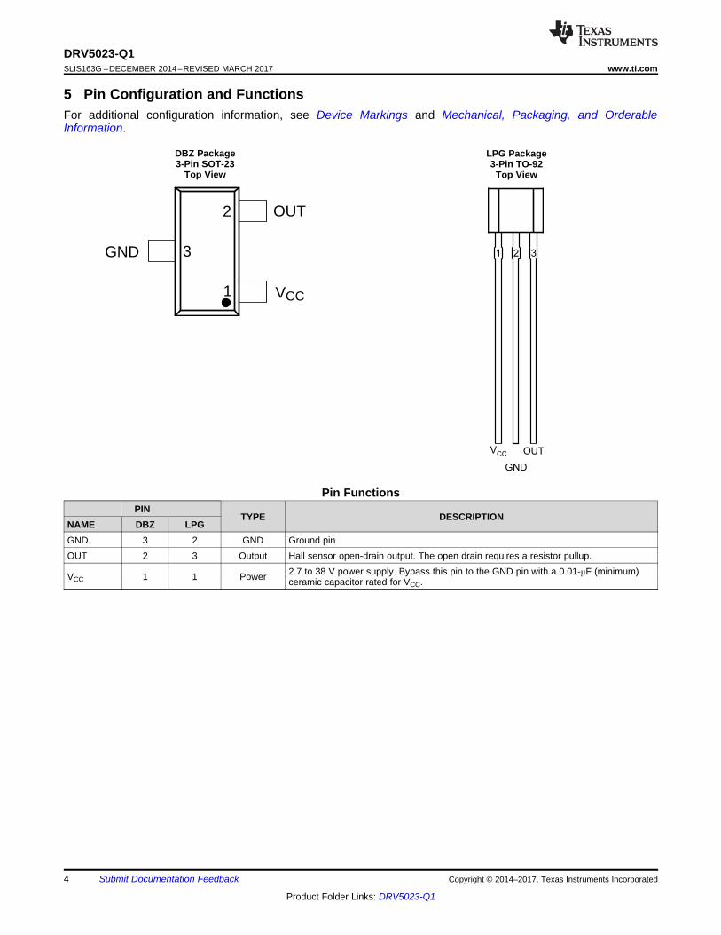
5 Pin Configuration and FunctionsFor additional configuration information, see Device Markings and Mechanical, Packaging, and OrderableInformation.
DBZ Package3-Pin SOT-23
Top View
LPG Package3-Pin TO-92
Top View
Pin FunctionsPIN
TYPE DESCRIPTIONNAME DBZ LPGGND 3 2 GND Ground pinOUT 2 3 Output Hall sensor open-drain output. The open drain requires a resistor pullup.
VCC 1 1 Power 2.7 to 38 V power supply. Bypass this pin to the GND pin with a 0.01-μF (minimum)ceramic capacitor rated for VCC.
5
DRV5023-Q1www.ti.com SLIS163G –DECEMBER 2014–REVISED MARCH 2017
Product Folder Links: DRV5023-Q1
Submit Documentation FeedbackCopyright © 2014–2017, Texas Instruments Incorporated
(1) Stresses beyond those listed under Absolute Maximum Ratings may cause permanent damage to the device. These are stress ratingsonly, which do not imply functional operation of the device at these or any other conditions beyond those indicated under RecommendedOperating Conditions. Exposure to absolute-maximum-rated conditions for extended periods may affect device reliability.
(2) Ensured by design. Only tested to –20 V.
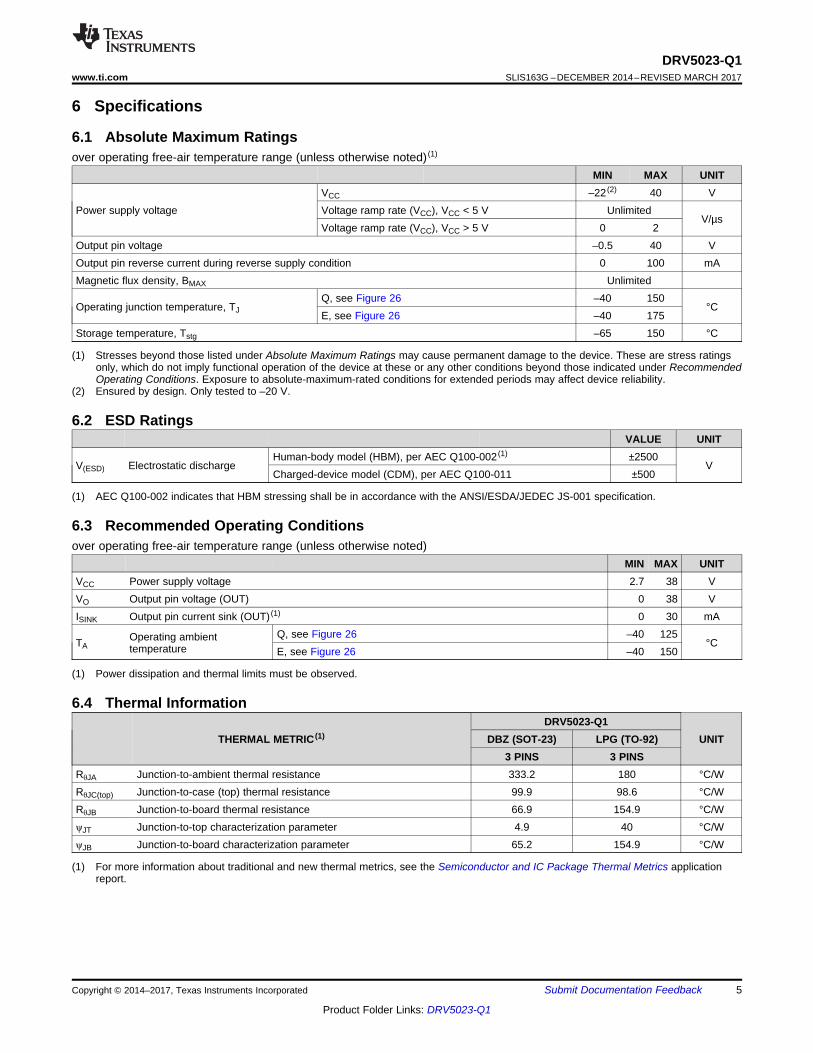
6 Specifications
6.1 Absolute Maximum Ratingsover operating free-air temperature range (unless otherwise noted) (1)
MIN MAX UNIT
Power supply voltageVCC –22 (2) 40 VVoltage ramp rate (VCC), VCC < 5 V Unlimited
V/µsVoltage ramp rate (VCC), VCC > 5 V 0 2
Output pin voltage –0.5 40 VOutput pin reverse current during reverse supply condition 0 100 mAMagnetic flux density, BMAX Unlimited
Operating junction temperature, TJQ, see Figure 26 –40 150
°CE, see Figure 26 –40 175
Storage temperature, Tstg –65 150 °C
(1) AEC Q100-002 indicates that HBM stressing shall be in accordance with the ANSI/ESDA/JEDEC JS-001 specification.
6.2 ESD RatingsVALUE UNIT
V(ESD) Electrostatic dischargeHuman-body model (HBM), per AEC Q100-002 (1) ±2500
VCharged-device model (CDM), per AEC Q100-011 ±500
(1) Power dissipation and thermal limits must be observed.
6.3 Recommended Operating Conditionsover operating free-air temperature range (unless otherwise noted)
MIN MAX UNITVCC Power supply voltage 2.7 38 VVO Output pin voltage (OUT) 0 38 VISINK Output pin current sink (OUT) (1) 0 30 mA
TAOperating ambienttemperature
Q, see Figure 26 –40 125°C
E, see Figure 26 –40 150
(1) For more information about traditional and new thermal metrics, see the Semiconductor and IC Package Thermal Metrics applicationreport.
6.4 Thermal Information
THERMAL METRIC (1)DRV5023-Q1
UNITDBZ (SOT-23) LPG (TO-92)3 PINS 3 PINS
RθJA Junction-to-ambient thermal resistance 333.2 180 °C/WRθJC(top) Junction-to-case (top) thermal resistance 99.9 98.6 °C/WRθJB Junction-to-board thermal resistance 66.9 154.9 °C/WψJT Junction-to-top characterization parameter 4.9 40 °C/WψJB Junction-to-board characterization parameter 65.2 154.9 °C/W
6
DRV5023-Q1SLIS163G –DECEMBER 2014–REVISED MARCH 2017 www.ti.com
Product Folder Links: DRV5023-Q1
Submit Documentation Feedback Copyright © 2014–2017, Texas Instruments Incorporated
(1) TA, MAX is 125°C for Q Grade 1 devices and 150°C for E Grade 0 devices (see Figure 26)
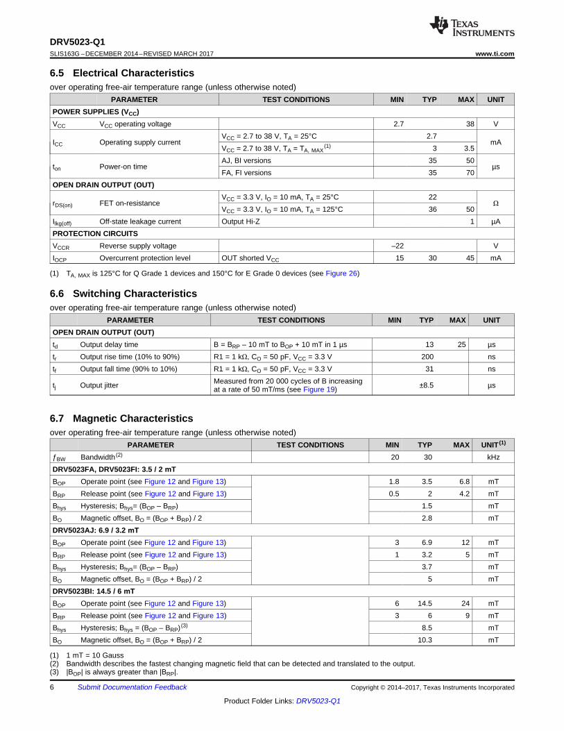
6.5 Electrical Characteristicsover operating free-air temperature range (unless otherwise noted)
PARAMETER TEST CONDITIONS MIN TYP MAX UNITPOWER SUPPLIES (VCC)VCC VCC operating voltage 2.7 38 V
ICC Operating supply currentVCC = 2.7 to 38 V, TA = 25°C 2.7
mAVCC = 2.7 to 38 V, TA = TA, MAX
(1) 3 3.5
ton Power-on timeAJ, BI versions 35 50
µsFA, FI versions 35 70
OPEN DRAIN OUTPUT (OUT)
rDS(on) FET on-resistanceVCC = 3.3 V, IO = 10 mA, TA = 25°C 22
ΩVCC = 3.3 V, IO = 10 mA, TA = 125°C 36 50
Ilkg(off) Off-state leakage current Output Hi-Z 1 µAPROTECTION CIRCUITSVCCR Reverse supply voltage –22 VIOCP Overcurrent protection level OUT shorted VCC 15 30 45 mA
6.6 Switching Characteristicsover operating free-air temperature range (unless otherwise noted)
PARAMETER TEST CONDITIONS MIN TYP MAX UNITOPEN DRAIN OUTPUT (OUT)td Output delay time B = BRP – 10 mT to BOP + 10 mT in 1 µs 13 25 µstr Output rise time (10% to 90%) R1 = 1 kΩ, CO = 50 pF, VCC = 3.3 V 200 nstf Output fall time (90% to 10%) R1 = 1 kΩ, CO = 50 pF, VCC = 3.3 V 31 ns
tj Output jitter Measured from 20 000 cycles of B increasingat a rate of 50 mT/ms (see Figure 19) ±8.5 µs
(1) 1 mT = 10 Gauss(2) Bandwidth describes the fastest changing magnetic field that can be detected and translated to the output.(3) |BOP| is always greater than |BRP|.
6.7 Magnetic Characteristicsover operating free-air temperature range (unless otherwise noted)
PARAMETER TEST CONDITIONS MIN TYP MAX UNIT (1)
ƒBW Bandwidth (2) 20 30 kHzDRV5023FA, DRV5023FI: 3.5 / 2 mTBOP Operate point (see Figure 12 and Figure 13) 1.8 3.5 6.8 mTBRP Release point (see Figure 12 and Figure 13) 0.5 2 4.2 mTBhys Hysteresis; Bhys= (BOP – BRP) 1.5 mTBO Magnetic offset, BO = (BOP + BRP) / 2 2.8 mTDRV5023AJ: 6.9 / 3.2 mTBOP Operate point (see Figure 12 and Figure 13) 3 6.9 12 mTBRP Release point (see Figure 12 and Figure 13) 1 3.2 5 mTBhys Hysteresis; Bhys= (BOP – BRP) 3.7 mTBO Magnetic offset, BO = (BOP + BRP) / 2 5 mTDRV5023BI: 14.5 / 6 mTBOP Operate point (see Figure 12 and Figure 13) 6 14.5 24 mTBRP Release point (see Figure 12 and Figure 13) 3 6 9 mTBhys Hysteresis; Bhys = (BOP – BRP) (3) 8.5 mTBO Magnetic offset, BO = (BOP + BRP) / 2 10.3 mT
Supply Voltage (V)
Mag
netic
Fie
ld R
elea
se P
oint
BR
P (
mT
)
0 10 20 30 402
2.5
3
3.5
4
4.5
5
5.5
6
6.5
D003
DRV5023BIDRV5023AJ
Ambient Temperature (°C)
Mag
netic
Fie
ld O
pera
te P
oint
BR
P (
mT
)
-50 -25 0 25 50 75 100 125 1502
3
4
5
6
7
D004
DRV5023AJDRV5023BI
Supply Voltage (V)
Mag
netic
Fie
ld O
pera
te P
oint
BO
P (
mT
)
0 10 20 30 404
6
8
10
12
14
16
D001
DRV5023AJDRV5023BI
Ambient Temperature (°C)
Mag
netic
Fie
ld O
pera
te P
oint
BO
P (
mT
)
-50 -25 0 25 50 75 100 125 1504
6
8
10
12
14
16
D002
DRV5023AJDRV5023BI
Supply Voltage (V)
Sup
ply
Cur
rent
(m
A)
0 10 20 30 402
2.5
3
3.5
D009
TA ±&
TA = 25°CTA = 75°C
TA = 125°CTA = 150°C
Ambient Temperature (°C)
Sup
ply
Cur
rent
(m
A)
-50 -25 0 25 50 75 100 125 1502
2.5
3
3.5
D010
VCC = 3.3 VVCC = 13.2 VVCC = 38 V
7
DRV5023-Q1www.ti.com SLIS163G –DECEMBER 2014–REVISED MARCH 2017
Product Folder Links: DRV5023-Q1
Submit Documentation FeedbackCopyright © 2014–2017, Texas Instruments Incorporated
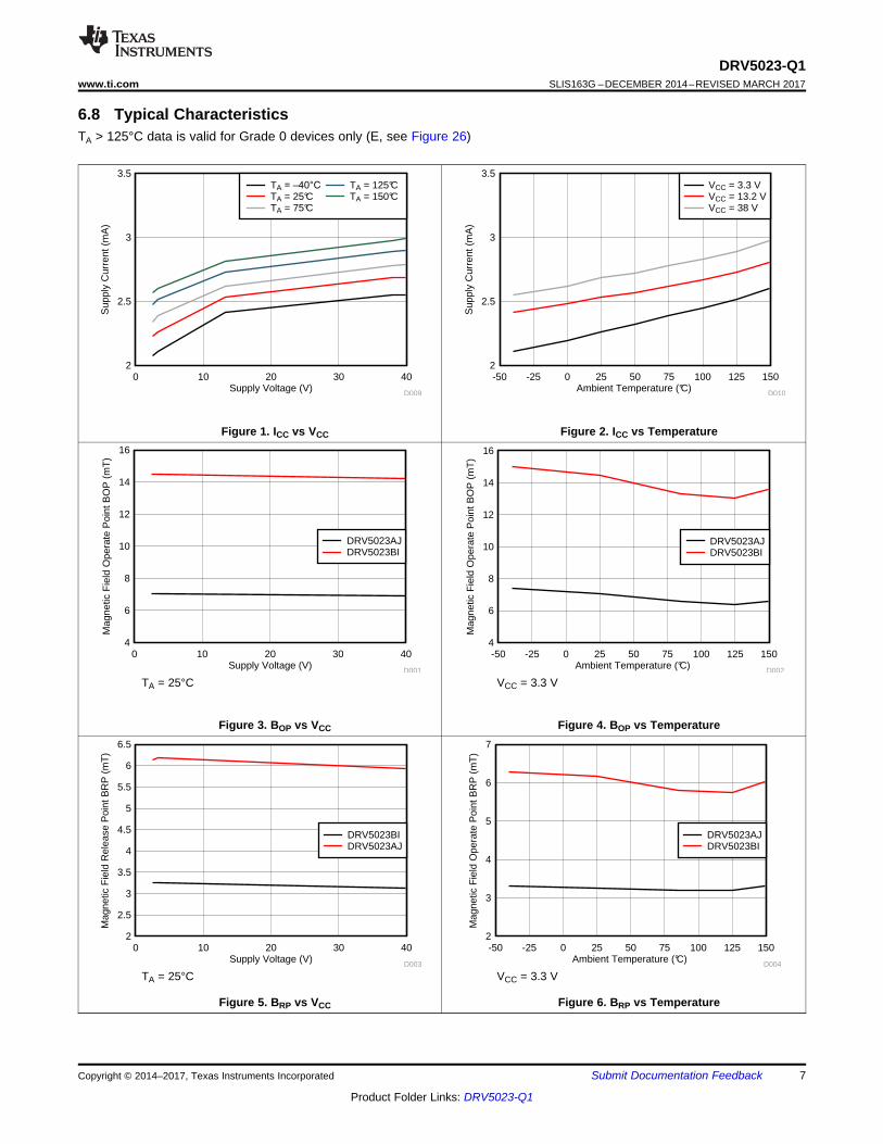
6.8 Typical CharacteristicsTA > 125°C data is valid for Grade 0 devices only (E, see Figure 26)
Figure 1. ICC vs VCC Figure 2. ICC vs Temperature
TA = 25°C
Figure 3. BOP vs VCC
VCC = 3.3 V
Figure 4. BOP vs Temperature
TA = 25°C
Figure 5. BRP vs VCC
VCC = 3.3 V
Figure 6. BRP vs Temperature
Supply Voltage (V)
Offs
et (
mT
)
0 4 8 12 16 20 24 28 32 36 404
5
6
7
8
9
10
11
D005
DRV5023AJDRV5023BI
Ambient Temperature (°C)
Offs
et (
mT
)
-50 -25 0 25 50 75 100 125 1504
5
6
7
8
9
10
11
D006
DRV5023AJDRV5023BI
Supply Voltage (V)
Hys
tere
sis
(mT
)
0 10 20 30 402
3
4
5
6
7
8
9
D007
DRV5023AJDRV5023BI
Ambient Temperature (°C)
Hys
tere
sis
(mT
)
-50 -25 0 25 50 75 100 125 1502
4
6
8
10
D008
DRV5023AJDRV5023BI
8
DRV5023-Q1SLIS163G –DECEMBER 2014–REVISED MARCH 2017 www.ti.com
Product Folder Links: DRV5023-Q1
Submit Documentation Feedback Copyright © 2014–2017, Texas Instruments Incorporated
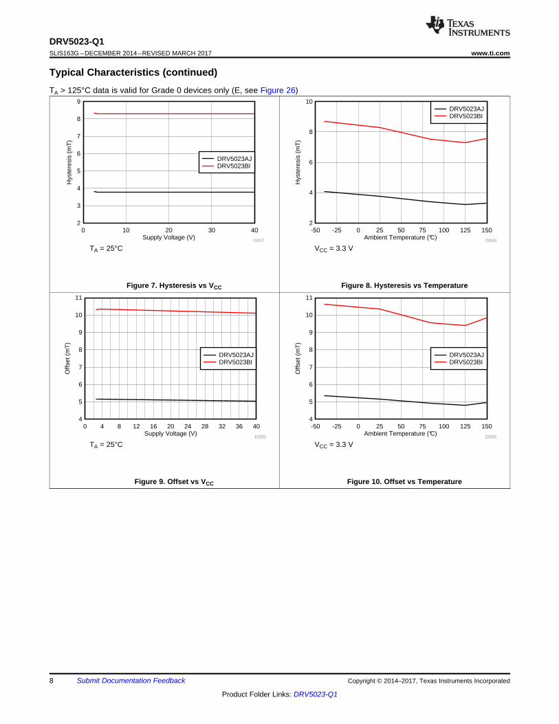
Typical Characteristics (continued)TA > 125°C data is valid for Grade 0 devices only (E, see Figure 26)
TA = 25°C
Figure 7. Hysteresis vs VCC
VCC = 3.3 V
Figure 8. Hysteresis vs Temperature
TA = 25°C
Figure 9. Offset vs VCC
VCC = 3.3 V
Figure 10. Offset vs Temperature
Temperature Compensation
Bias
+
±
Offset C
ancel
Regulated Supply
Reference
Gate Drive
OCP
VCC
OUT
GND
2.7 V to 38 V
R1
C2(Optional)
C1
Hall Element
9
DRV5023-Q1www.ti.com SLIS163G –DECEMBER 2014–REVISED MARCH 2017
Product Folder Links: DRV5023-Q1
Submit Documentation FeedbackCopyright © 2014–2017, Texas Instruments Incorporated
7 Detailed Description
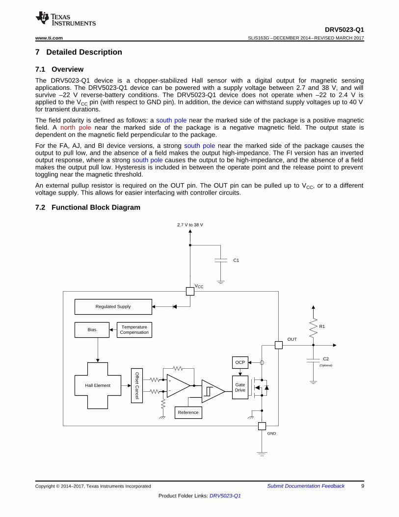
7.1 OverviewThe DRV5023-Q1 device is a chopper-stabilized Hall sensor with a digital output for magnetic sensingapplications. The DRV5023-Q1 device can be powered with a supply voltage between 2.7 and 38 V, and willsurvive –22 V reverse-battery conditions. The DRV5023-Q1 device does not operate when –22 to 2.4 V isapplied to the VCC pin (with respect to GND pin). In addition, the device can withstand supply voltages up to 40 Vfor transient durations.
The field polarity is defined as follows: a south pole near the marked side of the package is a positive magneticfield. A north pole near the marked side of the package is a negative magnetic field. The output state isdependent on the magnetic field perpendicular to the package.
For the FA, AJ, and BI device versions, a strong south pole near the marked side of the package causes theoutput to pull low, and the absence of a field makes the output high-impedance. The FI version has an invertedoutput response, where a strong south pole causes the output to be high-impedance, and the absence of a fieldmakes the output pull low. Hysteresis is included in between the operate point and the release point to preventtoggling near the magnetic threshold.
An external pullup resistor is required on the OUT pin. The OUT pin can be pulled up to VCC, or to a differentvoltage supply. This allows for easier interfacing with controller circuits.
7.2 Functional Block Diagram

OUT
BOPBRP BOF
Bhys
B (mT)
OUT
BOPBRP BOF
Bhys
B (mT)
1 2 3
S
N
B > 0 mT
S
N
B < 0 mT
S
N
B > 0 mT
S
N
B < 0 mT
(Bottom view)
SOT-23 (DBZ) TO-92 (LPG)
1 2 3
10
DRV5023-Q1SLIS163G –DECEMBER 2014–REVISED MARCH 2017 www.ti.com
Product Folder Links: DRV5023-Q1
Submit Documentation Feedback Copyright © 2014–2017, Texas Instruments Incorporated
7.3 Feature Description
7.3.1 Field Direction DefinitionA positive magnetic field is defined as a south pole near the marked side of the package as shown in Figure 11.
N = North pole, S = South pole
Figure 11. Field Direction Definition
7.3.2 Device OutputIf the device is powered on with a magnetic field strength between BRP and BOP, then the device output isindeterminate and can either be Hi-Z or Low. For the FA, AJ, and BI device versions, if the field strength isgreater than BOP, then the output is pulled low; if the field strength is less than BRP, then the output is released.For the FI device version, if the field strength is greater than BOP, then the output is Hi-Z; if the field strength isless than BRP, then the output is pulled Low.
Figure 12. Output State of FA, AJ, BI Versions
Figure 13. Output State of FI Version

VCC
BOP
BRP
t (s)
B (mT)
t (s)
OUT
t (s)
Valid Output
ton
VCC
BOP
BRP
t (s)
B (mT)
t (s)
t (s)
OUT
Valid Output
ton
11
DRV5023-Q1www.ti.com SLIS163G –DECEMBER 2014–REVISED MARCH 2017
Product Folder Links: DRV5023-Q1
Submit Documentation FeedbackCopyright © 2014–2017, Texas Instruments Incorporated
Feature Description (continued)7.3.3 Power-On TimeAfter applying VCC to the DRV5023-Q1 device, ton must elapse before the OUT pin is valid. During the power-upsequence, the output is Hi-Z. A pulse as shown in Figure 14 and Figure 15 occurs at the end of ton. This pulsecan allow the host processor to determine when the DRV5023-Q1 output is valid after startup. In Case 1(Figure 14) and Case 2 (Figure 15), the output is defined assuming a constant magnetic field B > BOP and B <BRP.
Figure 14. Case 1: Power On When B > BOP
Figure 15. Case 2: Power On When B < BRP

VCC
BOP
BRPt (s)
B (mT)
t (s)
t (s)
OUT
Valid Output
tdton
12
DRV5023-Q1SLIS163G –DECEMBER 2014–REVISED MARCH 2017 www.ti.com
Product Folder Links: DRV5023-Q1
Submit Documentation Feedback Copyright © 2014–2017, Texas Instruments Incorporated
Feature Description (continued)If the device is powered on with the magnetic field strength BRP < B < BOP, then the device output isindeterminate and can either be Hi-Z or pulled low. During the power-up sequence, the output is held Hi-Z untilton has elapsed. At the end of ton, a pulse is given on the OUT pin to indicate that ton has elapsed. After ton, if themagnetic field changes such that BOP < B, the output is released. Case 3 (Figure 16) and Case 4 (Figure 17)show examples of this behavior.
Figure 16. Case 3: Power On When BRP < B < BOP, Followed by B > BOP

VCC
BOP
BRP
t (s)
B (mT)
t (s)
t (s)
OUT
Valid Output
tdton
13
DRV5023-Q1www.ti.com SLIS163G –DECEMBER 2014–REVISED MARCH 2017
Product Folder Links: DRV5023-Q1
Submit Documentation FeedbackCopyright © 2014–2017, Texas Instruments Incorporated
Feature Description (continued)
Figure 17. Case 4: Power On When BRP < B < BOP, Followed by B < BRP
BW1
¦ +]2 R1 C2
u S u u
Gate Drive
OCP
OUT
GND
R1
C2
Vref
ISINK
ref refV max V minR1
30 mA 100 µAd d
14
DRV5023-Q1SLIS163G –DECEMBER 2014–REVISED MARCH 2017 www.ti.com
Product Folder Links: DRV5023-Q1
Submit Documentation Feedback Copyright © 2014–2017, Texas Instruments Incorporated
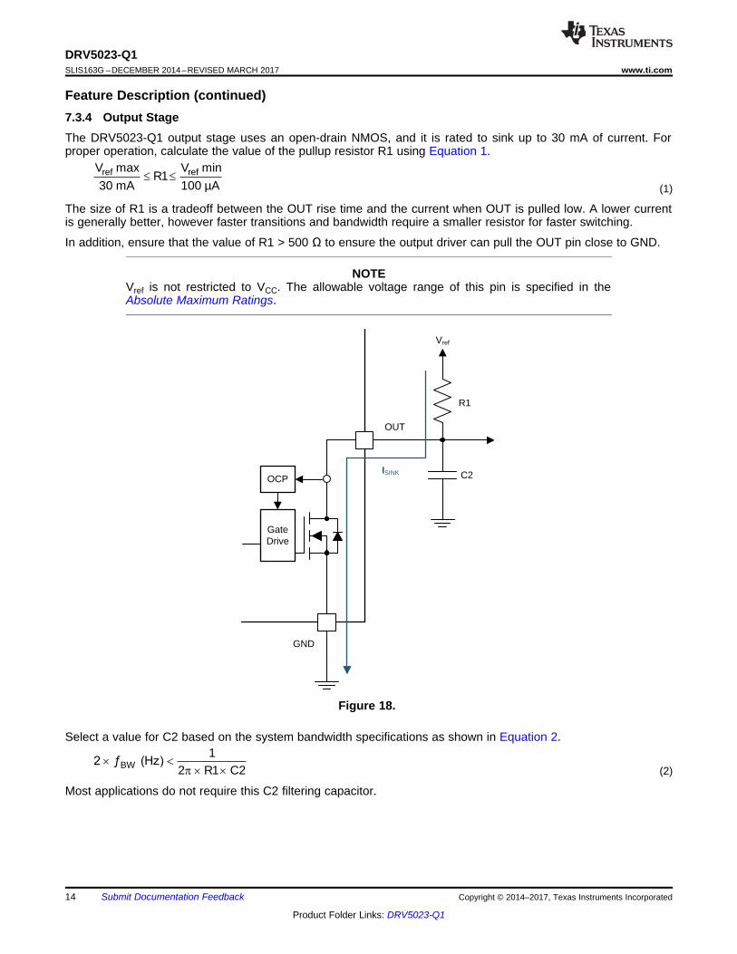
Feature Description (continued)7.3.4 Output StageThe DRV5023-Q1 output stage uses an open-drain NMOS, and it is rated to sink up to 30 mA of current. Forproper operation, calculate the value of the pullup resistor R1 using Equation 1.
(1)
The size of R1 is a tradeoff between the OUT rise time and the current when OUT is pulled low. A lower currentis generally better, however faster transitions and bandwidth require a smaller resistor for faster switching.
In addition, ensure that the value of R1 > 500 Ω to ensure the output driver can pull the OUT pin close to GND.
NOTEVref is not restricted to VCC. The allowable voltage range of this pin is specified in theAbsolute Maximum Ratings.
Figure 18.
Select a value for C2 based on the system bandwidth specifications as shown in Equation 2.
(2)
Most applications do not require this C2 filtering capacitor.
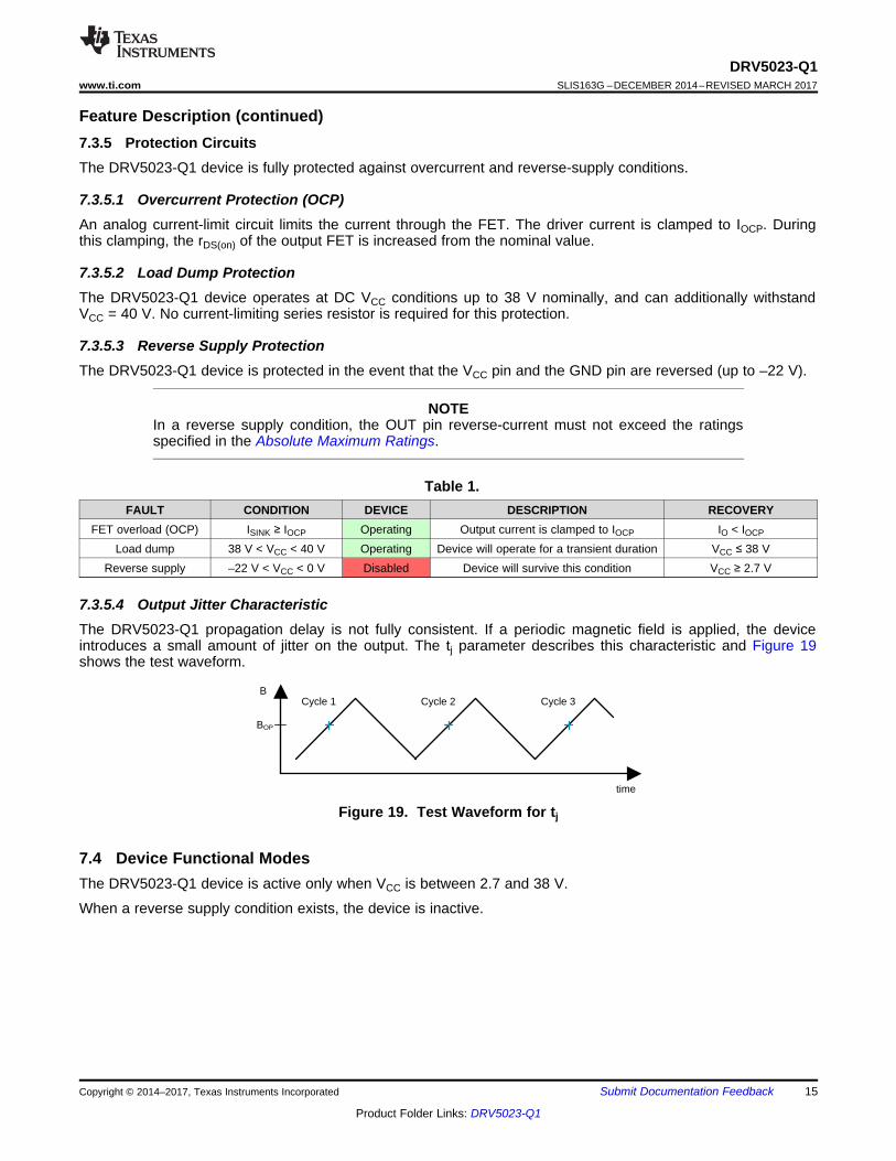
BCycle 1 Cycle 2 Cycle 3
time
BOP
15
DRV5023-Q1www.ti.com SLIS163G –DECEMBER 2014–REVISED MARCH 2017
Product Folder Links: DRV5023-Q1
Submit Documentation FeedbackCopyright © 2014–2017, Texas Instruments Incorporated
Feature Description (continued)7.3.5 Protection CircuitsThe DRV5023-Q1 device is fully protected against overcurrent and reverse-supply conditions.
7.3.5.1 Overcurrent Protection (OCP)An analog current-limit circuit limits the current through the FET. The driver current is clamped to IOCP. Duringthis clamping, the rDS(on) of the output FET is increased from the nominal value.
7.3.5.2 Load Dump ProtectionThe DRV5023-Q1 device operates at DC VCC conditions up to 38 V nominally, and can additionally withstandVCC = 40 V. No current-limiting series resistor is required for this protection.
7.3.5.3 Reverse Supply ProtectionThe DRV5023-Q1 device is protected in the event that the VCC pin and the GND pin are reversed (up to –22 V).
NOTEIn a reverse supply condition, the OUT pin reverse-current must not exceed the ratingsspecified in the Absolute Maximum Ratings.
Table 1.FAULT CONDITION DEVICE DESCRIPTION RECOVERY
FET overload (OCP) ISINK ≥ IOCP Operating Output current is clamped to IOCP IO < IOCP
Load dump 38 V < VCC < 40 V Operating Device will operate for a transient duration VCC ≤ 38 VReverse supply –22 V < VCC < 0 V Disabled Device will survive this condition VCC ≥ 2.7 V
7.3.5.4 Output Jitter CharacteristicThe DRV5023-Q1 propagation delay is not fully consistent. If a periodic magnetic field is applied, the deviceintroduces a small amount of jitter on the output. The tj parameter describes this characteristic and Figure 19shows the test waveform.
Figure 19. Test Waveform for tj
7.4 Device Functional ModesThe DRV5023-Q1 device is active only when VCC is between 2.7 and 38 V.
When a reverse supply condition exists, the device is inactive.
2
1
3
C10.01 µF
(minimum)
OUT
VCC
R110 k
C2680 pF
(Optional)
VCC
16
DRV5023-Q1SLIS163G –DECEMBER 2014–REVISED MARCH 2017 www.ti.com
Product Folder Links: DRV5023-Q1
Submit Documentation Feedback Copyright © 2014–2017, Texas Instruments Incorporated
8 Application and Implementation
NOTEInformation in the following applications sections is not part of the TI componentspecification, and TI does not warrant its accuracy or completeness. TI’s customers areresponsible for determining suitability of components for their purposes. Customers shouldvalidate and test their design implementation to confirm system functionality.
8.1 Application InformationThe DRV5023-Q1 device is used in magnetic-field sensing applications.
8.2 Typical Applications
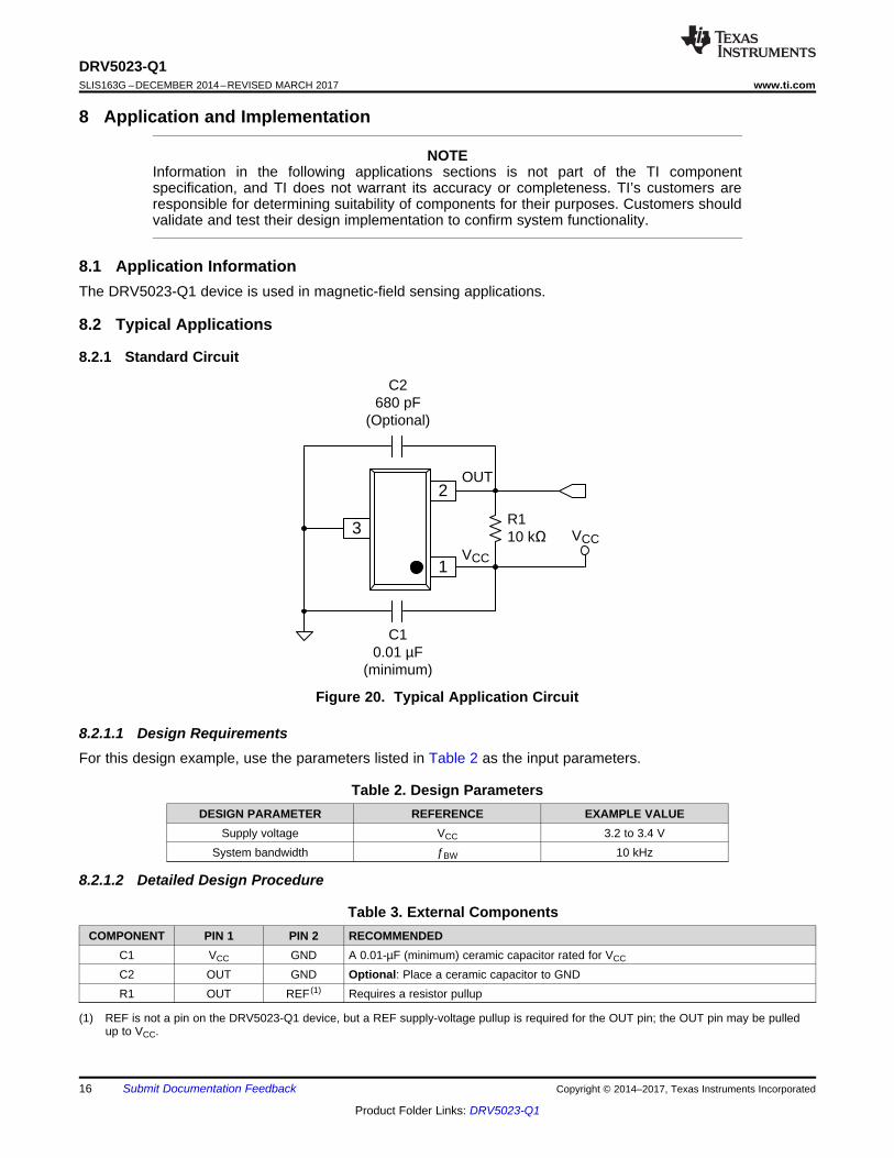
8.2.1 Standard Circuit
Figure 20. Typical Application Circuit
8.2.1.1 Design RequirementsFor this design example, use the parameters listed in Table 2 as the input parameters.
Table 2. Design ParametersDESIGN PARAMETER REFERENCE EXAMPLE VALUE
Supply voltage VCC 3.2 to 3.4 VSystem bandwidth ƒBW 10 kHz
(1) REF is not a pin on the DRV5023-Q1 device, but a REF supply-voltage pullup is required for the OUT pin; the OUT pin may be pulledup to VCC.
8.2.1.2 Detailed Design Procedure
Table 3. External ComponentsCOMPONENT PIN 1 PIN 2 RECOMMENDED
C1 VCC GND A 0.01-µF (minimum) ceramic capacitor rated for VCC
C2 OUT GND Optional: Place a ceramic capacitor to GNDR1 OUT REF (1) Requires a resistor pullup
Frequency (Hz)
Mag
nitu
de (
dB)
100 1000 10000 100000-14
-12
-10
-8
-6
-4
-2
0
D011
OUT OUT
12 10 kHz
2 R1 C2u
S u u
BW1
¦ +]2 R1 C2
u S u u
3.4 V 3.2 VR1
30 mA 100 µAd d
ref refV max V minR1
30 mA 100 µAd d
17
DRV5023-Q1www.ti.com SLIS163G –DECEMBER 2014–REVISED MARCH 2017
Product Folder Links: DRV5023-Q1
Submit Documentation FeedbackCopyright © 2014–2017, Texas Instruments Incorporated
8.2.1.2.1 Configuration Example
In a 3.3-V system, 3.2 V ≤ Vref ≤ 3.4 V. Use Equation 3 to calculate the allowable range for R1.
(3)
For this design example, use Equation 4 to calculate the allowable range of R1.
(4)
Therefore:113 Ω ≤ R1 ≤ 32 kΩ (5)
After finding the allowable range of R1 (Equation 5), select a value between 500 Ω and 32 kΩ for R1.
Assuming a system bandwidth of 10 kHz, use Equation 6 to calculate the value of C2.
(6)
For this design example, use Equation 7 to calculate the value of C2.
(7)
An R1 value of 10 kΩ and a C2 value less than 820 pF satisfy the requirement for a 10-kHz system bandwidth.
A selection of R1 = 10 kΩ and C2 = 680 pF would cause a low-pass filter with a corner frequency of 23.4 kHz.
8.2.1.3 Application Curves
R1 = 10-kΩ pullup No C2
Figure 21. 10-kHz Switching Magnetic Field
R1 = 10-kΩ pullup C2 = 680 pF
Figure 22. 10-kHz Switching Magnetic Field
R1 = 10-kΩ pullup C2 = 680 pF
Figure 23. Low-Pass Filtering

OUT VCC
R1
GND3
2 1
Controller
+±
Current sense
C1
18
DRV5023-Q1SLIS163G –DECEMBER 2014–REVISED MARCH 2017 www.ti.com
Product Folder Links: DRV5023-Q1
Submit Documentation Feedback Copyright © 2014–2017, Texas Instruments Incorporated
8.2.2 Alternative Two-Wire ApplicationFor systems that require minimal wire count, the device output can be connected to VCC through a resistor, andthe total supplied current can be sensed near the controller.
Figure 24. 2-Wire Application
Current can be sensed using a shunt resistor or other circuitry.
8.2.2.1 Design RequirementsTable 4 lists the related design parameters.
Table 4. Design ParametersDESIGN PARAMETER REFERENCE EXAMPLE VALUE
Supply voltage VCC 12 VOUT resistor R1 1 kΩBypass capacitor C1 0.1 µFCurrent when B < BRP IRELEASE About 3 mACurrent when B > BOP IOPERATE About 15 mA
8.2.2.2 Detailed Design ProcedureWhen the open-drain output of the device is high-impedance, current through the path equals the ICC of thedevice (approximately 3 mA).
When the output pulls low, a parallel current path is added, equal to VCC / (R1 + rDS(on)). Using 12 V and 1 kΩ,the parallel current is approximately 12 mA, making the total current approximately 15 mA.
The local bypass capacitor C1 should be at least 0.1 µF, and a larger value if there is high inductance in thepower line interconnect.
9 Power Supply RecommendationsThe DRV5023-Q1 device is designed to operate from an input voltage supply (VM) range between 2.7 and 38 V.A 0.01-µF (minimum) ceramic capacitor rated for VCC must be placed as close to the DRV5023-Q1 device aspossible.
GND
OUT VCC
19
DRV5023-Q1www.ti.com SLIS163G –DECEMBER 2014–REVISED MARCH 2017
Product Folder Links: DRV5023-Q1
Submit Documentation FeedbackCopyright © 2014–2017, Texas Instruments Incorporated
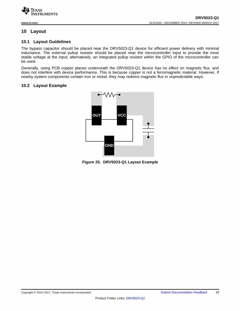
10 Layout
10.1 Layout GuidelinesThe bypass capacitor should be placed near the DRV5023-Q1 device for efficient power delivery with minimalinductance. The external pullup resistor should be placed near the microcontroller input to provide the moststable voltage at the input; alternatively, an integrated pullup resistor within the GPIO of the microcontroller canbe used.
Generally, using PCB copper planes underneath the DRV5023-Q1 device has no effect on magnetic flux, anddoes not interfere with device performance. This is because copper is not a ferromagnetic material. However, Ifnearby system components contain iron or nickel, they may redirect magnetic flux in unpredictable ways.
10.2 Layout Example
Figure 25. DRV5023-Q1 Layout Example
(Bottom view)1 2 3
Marked Side Front
Marked Side
1 2 31 2
3
Marked Side
(DBZ)(AJ)DRV5023
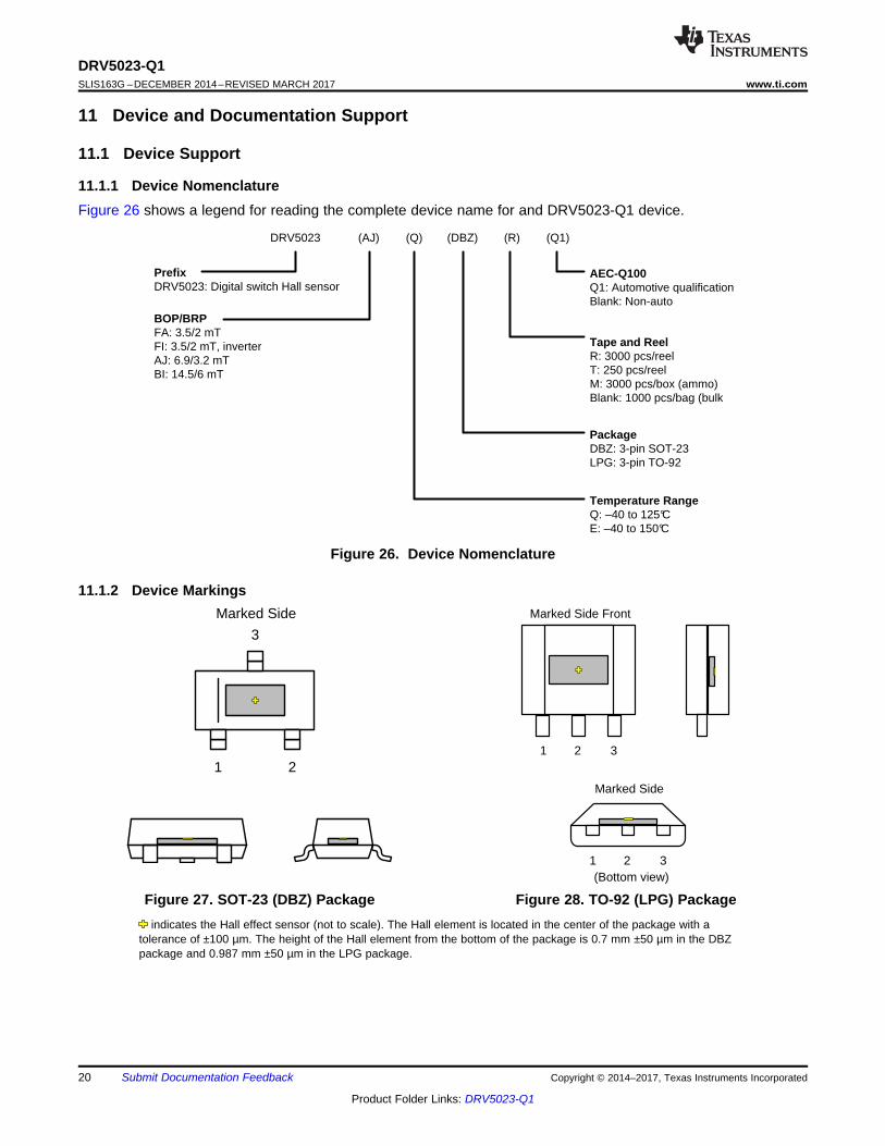
PrefixDRV5023: Digital switch Hall sensor
(Q) (R) (Q1)
AEC-Q100 Q1: Automotive qualificationBlank: Non-auto
PackageDBZ: 3-pin SOT-23LPG: 3-pin TO-92
Temperature RangeQ: ±40 to 125°CE: ±40 to 150°C
BOP/BRPFA: 3.5/2 mTFI: 3.5/2 mT, inverterAJ: 6.9/3.2 mT BI: 14.5/6 mT
Tape and Reel R: 3000 pcs/reelT: 250 pcs/reelM: 3000 pcs/box (ammo)Blank: 1000 pcs/bag (bulk
20
DRV5023-Q1SLIS163G –DECEMBER 2014–REVISED MARCH 2017 www.ti.com
Product Folder Links: DRV5023-Q1
Submit Documentation Feedback Copyright © 2014–2017, Texas Instruments Incorporated
11 Device and Documentation Support
11.1 Device Support
11.1.1 Device NomenclatureFigure 26 shows a legend for reading the complete device name for and DRV5023-Q1 device.
Figure 26. Device Nomenclature
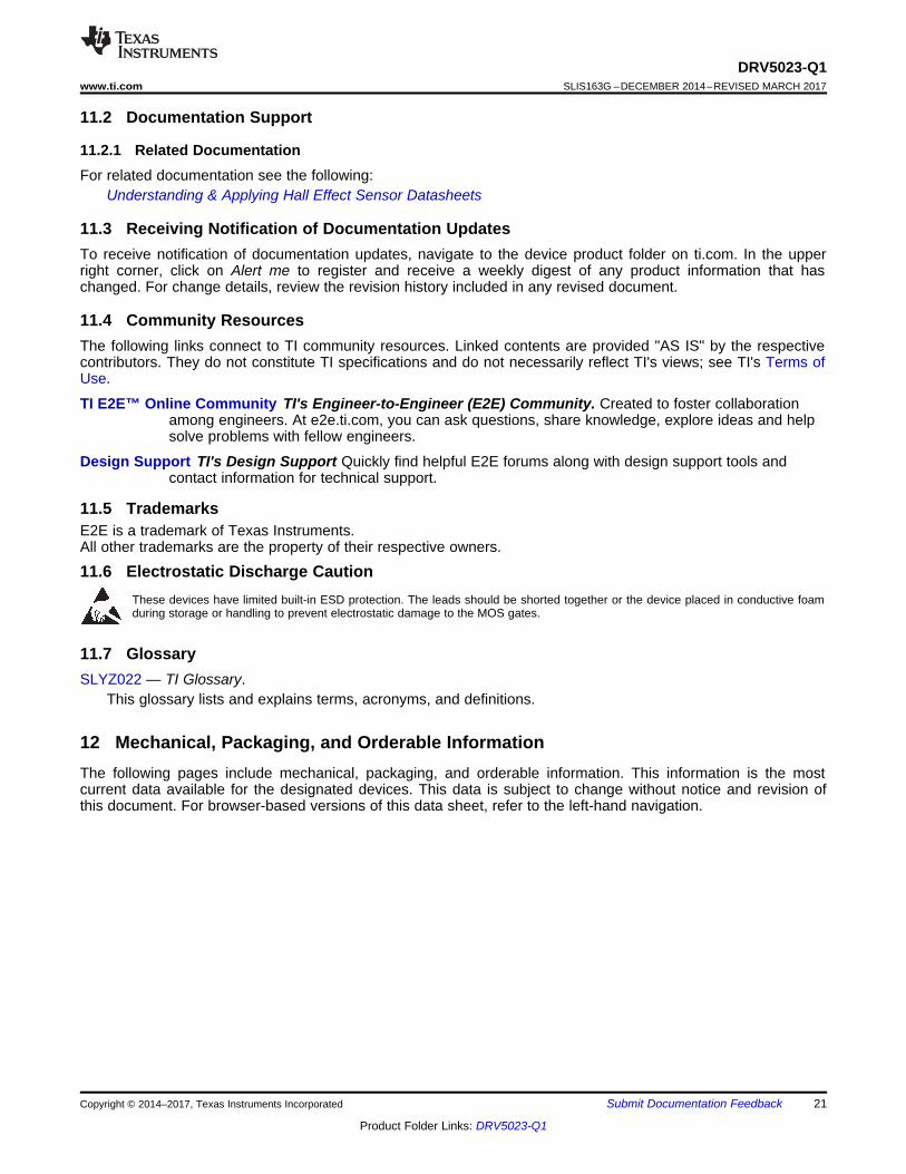
11.1.2 Device Markings
Figure 27. SOT-23 (DBZ) Package Figure 28. TO-92 (LPG) Packageindicates the Hall effect sensor (not to scale). The Hall element is located in the center of the package with a
tolerance of ±100 µm. The height of the Hall element from the bottom of the package is 0.7 mm ±50 µm in the DBZpackage and 0.987 mm ±50 µm in the LPG package.
21
DRV5023-Q1www.ti.com SLIS163G –DECEMBER 2014–REVISED MARCH 2017
Product Folder Links: DRV5023-Q1
Submit Documentation FeedbackCopyright © 2014–2017, Texas Instruments Incorporated
11.2 Documentation Support
11.2.1 Related DocumentationFor related documentation see the following:
Understanding & Applying Hall Effect Sensor Datasheets
11.3 Receiving Notification of Documentation UpdatesTo receive notification of documentation updates, navigate to the device product folder on ti.com. In the upperright corner, click on Alert me to register and receive a weekly digest of any product information that haschanged. For change details, review the revision history included in any revised document.
11.4 Community ResourcesThe following links connect to TI community resources. Linked contents are provided "AS IS" by the respectivecontributors. They do not constitute TI specifications and do not necessarily reflect TI's views; see TI's Terms ofUse.
TI E2E™ Online Community TI's Engineer-to-Engineer (E2E) Community. Created to foster collaborationamong engineers. At e2e.ti.com, you can ask questions, share knowledge, explore ideas and helpsolve problems with fellow engineers.
Design Support TI's Design Support Quickly find helpful E2E forums along with design support tools andcontact information for technical support.
11.5 TrademarksE2E is a trademark of Texas Instruments.All other trademarks are the property of their respective owners.
11.6 Electrostatic Discharge CautionThese devices have limited built-in ESD protection. The leads should be shorted together or the device placed in conductive foamduring storage or handling to prevent electrostatic damage to the MOS gates.
11.7 GlossarySLYZ022 — TI Glossary.
This glossary lists and explains terms, acronyms, and definitions.
12 Mechanical, Packaging, and Orderable InformationThe following pages include mechanical, packaging, and orderable information. This information is the mostcurrent data available for the designated devices. This data is subject to change without notice and revision ofthis document. For browser-based versions of this data sheet, refer to the left-hand navigation.
PACKAGE OPTION ADDENDUM
www.ti.com 27-Jan-2017
Addendum-Page 1
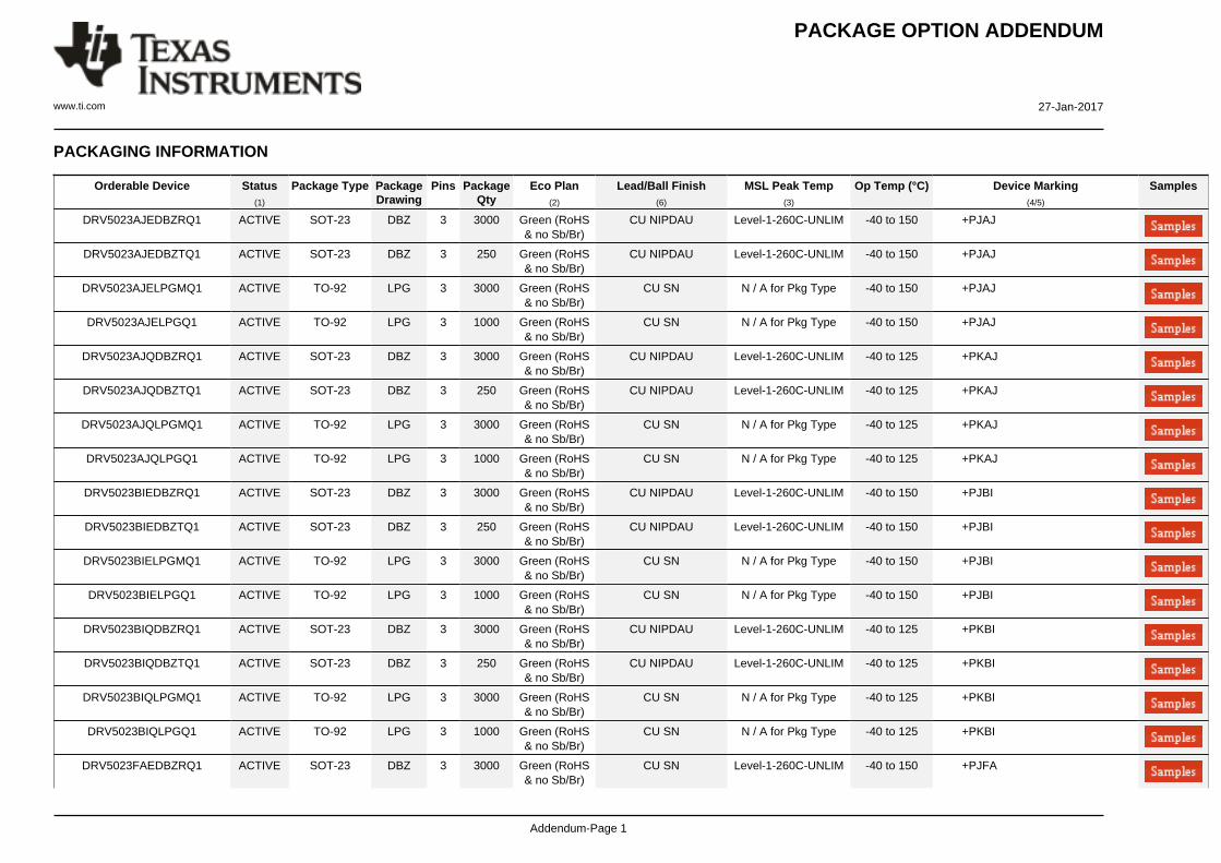
PACKAGING INFORMATION
Orderable Device Status(1)
Package Type PackageDrawing
Pins PackageQty
Eco Plan(2)
Lead/Ball Finish(6)
MSL Peak Temp(3)
Op Temp (°C) Device Marking(4/5)
Samples
DRV5023AJEDBZRQ1 ACTIVE SOT-23 DBZ 3 3000 Green (RoHS& no Sb/Br)
CU NIPDAU Level-1-260C-UNLIM -40 to 150 +PJAJ
DRV5023AJEDBZTQ1 ACTIVE SOT-23 DBZ 3 250 Green (RoHS& no Sb/Br)
CU NIPDAU Level-1-260C-UNLIM -40 to 150 +PJAJ
DRV5023AJELPGMQ1 ACTIVE TO-92 LPG 3 3000 Green (RoHS& no Sb/Br)
CU SN N / A for Pkg Type -40 to 150 +PJAJ
DRV5023AJELPGQ1 ACTIVE TO-92 LPG 3 1000 Green (RoHS& no Sb/Br)
CU SN N / A for Pkg Type -40 to 150 +PJAJ
DRV5023AJQDBZRQ1 ACTIVE SOT-23 DBZ 3 3000 Green (RoHS& no Sb/Br)
CU NIPDAU Level-1-260C-UNLIM -40 to 125 +PKAJ
DRV5023AJQDBZTQ1 ACTIVE SOT-23 DBZ 3 250 Green (RoHS& no Sb/Br)
CU NIPDAU Level-1-260C-UNLIM -40 to 125 +PKAJ
DRV5023AJQLPGMQ1 ACTIVE TO-92 LPG 3 3000 Green (RoHS& no Sb/Br)
CU SN N / A for Pkg Type -40 to 125 +PKAJ
DRV5023AJQLPGQ1 ACTIVE TO-92 LPG 3 1000 Green (RoHS& no Sb/Br)
CU SN N / A for Pkg Type -40 to 125 +PKAJ
DRV5023BIEDBZRQ1 ACTIVE SOT-23 DBZ 3 3000 Green (RoHS& no Sb/Br)
CU NIPDAU Level-1-260C-UNLIM -40 to 150 +PJBI
DRV5023BIEDBZTQ1 ACTIVE SOT-23 DBZ 3 250 Green (RoHS& no Sb/Br)
CU NIPDAU Level-1-260C-UNLIM -40 to 150 +PJBI
DRV5023BIELPGMQ1 ACTIVE TO-92 LPG 3 3000 Green (RoHS& no Sb/Br)
CU SN N / A for Pkg Type -40 to 150 +PJBI
DRV5023BIELPGQ1 ACTIVE TO-92 LPG 3 1000 Green (RoHS& no Sb/Br)
CU SN N / A for Pkg Type -40 to 150 +PJBI
DRV5023BIQDBZRQ1 ACTIVE SOT-23 DBZ 3 3000 Green (RoHS& no Sb/Br)
CU NIPDAU Level-1-260C-UNLIM -40 to 125 +PKBI
DRV5023BIQDBZTQ1 ACTIVE SOT-23 DBZ 3 250 Green (RoHS& no Sb/Br)
CU NIPDAU Level-1-260C-UNLIM -40 to 125 +PKBI
DRV5023BIQLPGMQ1 ACTIVE TO-92 LPG 3 3000 Green (RoHS& no Sb/Br)
CU SN N / A for Pkg Type -40 to 125 +PKBI
DRV5023BIQLPGQ1 ACTIVE TO-92 LPG 3 1000 Green (RoHS& no Sb/Br)
CU SN N / A for Pkg Type -40 to 125 +PKBI
DRV5023FAEDBZRQ1 ACTIVE SOT-23 DBZ 3 3000 Green (RoHS& no Sb/Br)
CU SN Level-1-260C-UNLIM -40 to 150 +PJFA
PACKAGE OPTION ADDENDUM
www.ti.com 27-Jan-2017
Addendum-Page 2
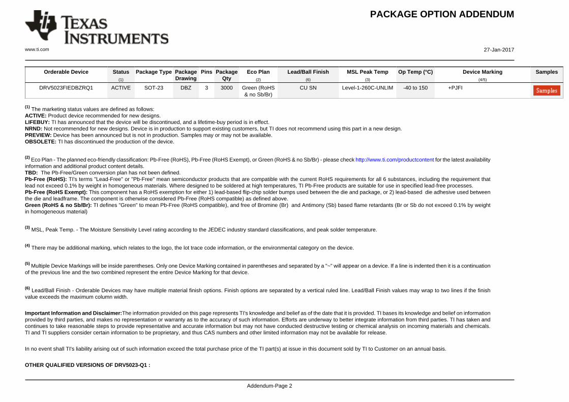
Orderable Device Status(1)
Package Type PackageDrawing
Pins PackageQty
Eco Plan(2)
Lead/Ball Finish(6)
MSL Peak Temp(3)
Op Temp (°C) Device Marking(4/5)
Samples
DRV5023FIEDBZRQ1 ACTIVE SOT-23 DBZ 3 3000 Green (RoHS& no Sb/Br)
CU SN Level-1-260C-UNLIM -40 to 150 +PJFI
(1) The marketing status values are defined as follows:ACTIVE: Product device recommended for new designs.LIFEBUY: TI has announced that the device will be discontinued, and a lifetime-buy period is in effect.NRND: Not recommended for new designs. Device is in production to support existing customers, but TI does not recommend using this part in a new design.PREVIEW: Device has been announced but is not in production. Samples may or may not be available.OBSOLETE: TI has discontinued the production of the device.
(2) Eco Plan - The planned eco-friendly classification: Pb-Free (RoHS), Pb-Free (RoHS Exempt), or Green (RoHS & no Sb/Br) - please check http://www.ti.com/productcontent for the latest availabilityinformation and additional product content details.TBD: The Pb-Free/Green conversion plan has not been defined.Pb-Free (RoHS): TI's terms "Lead-Free" or "Pb-Free" mean semiconductor products that are compatible with the current RoHS requirements for all 6 substances, including the requirement thatlead not exceed 0.1% by weight in homogeneous materials. Where designed to be soldered at high temperatures, TI Pb-Free products are suitable for use in specified lead-free processes.Pb-Free (RoHS Exempt): This component has a RoHS exemption for either 1) lead-based flip-chip solder bumps used between the die and package, or 2) lead-based die adhesive used betweenthe die and leadframe. The component is otherwise considered Pb-Free (RoHS compatible) as defined above.Green (RoHS & no Sb/Br): TI defines "Green" to mean Pb-Free (RoHS compatible), and free of Bromine (Br) and Antimony (Sb) based flame retardants (Br or Sb do not exceed 0.1% by weightin homogeneous material)
(3) MSL, Peak Temp. - The Moisture Sensitivity Level rating according to the JEDEC industry standard classifications, and peak solder temperature.
(4) There may be additional marking, which relates to the logo, the lot trace code information, or the environmental category on the device.
(5) Multiple Device Markings will be inside parentheses. Only one Device Marking contained in parentheses and separated by a "~" will appear on a device. If a line is indented then it is a continuationof the previous line and the two combined represent the entire Device Marking for that device.
(6) Lead/Ball Finish - Orderable Devices may have multiple material finish options. Finish options are separated by a vertical ruled line. Lead/Ball Finish values may wrap to two lines if the finishvalue exceeds the maximum column width.
Important Information and Disclaimer:The information provided on this page represents TI's knowledge and belief as of the date that it is provided. TI bases its knowledge and belief on informationprovided by third parties, and makes no representation or warranty as to the accuracy of such information. Efforts are underway to better integrate information from third parties. TI has taken andcontinues to take reasonable steps to provide representative and accurate information but may not have conducted destructive testing or chemical analysis on incoming materials and chemicals.TI and TI suppliers consider certain information to be proprietary, and thus CAS numbers and other limited information may not be available for release.
In no event shall TI's liability arising out of such information exceed the total purchase price of the TI part(s) at issue in this document sold by TI to Customer on an annual basis.
OTHER QUALIFIED VERSIONS OF DRV5023-Q1 :

PACKAGE OPTION ADDENDUM
www.ti.com 27-Jan-2017
Addendum-Page 3
• Catalog: DRV5023
NOTE: Qualified Version Definitions:
• Catalog - TI's standard catalog product
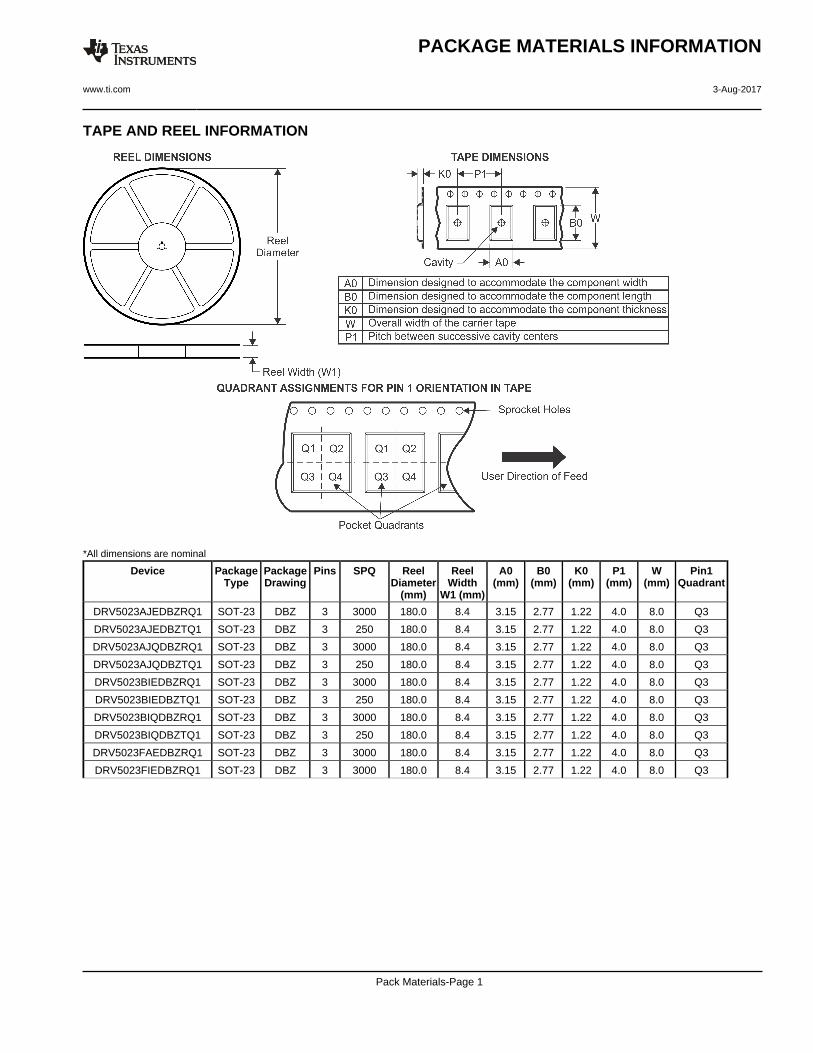
TAPE AND REEL INFORMATION
*All dimensions are nominal
Device PackageType
PackageDrawing
Pins SPQ ReelDiameter
(mm)
ReelWidth
W1 (mm)
A0(mm)
B0(mm)
K0(mm)
P1(mm)
W(mm)
Pin1Quadrant
DRV5023AJEDBZRQ1 SOT-23 DBZ 3 3000 180.0 8.4 3.15 2.77 1.22 4.0 8.0 Q3
DRV5023AJEDBZTQ1 SOT-23 DBZ 3 250 180.0 8.4 3.15 2.77 1.22 4.0 8.0 Q3
DRV5023AJQDBZRQ1 SOT-23 DBZ 3 3000 180.0 8.4 3.15 2.77 1.22 4.0 8.0 Q3
DRV5023AJQDBZTQ1 SOT-23 DBZ 3 250 180.0 8.4 3.15 2.77 1.22 4.0 8.0 Q3
DRV5023BIEDBZRQ1 SOT-23 DBZ 3 3000 180.0 8.4 3.15 2.77 1.22 4.0 8.0 Q3
DRV5023BIEDBZTQ1 SOT-23 DBZ 3 250 180.0 8.4 3.15 2.77 1.22 4.0 8.0 Q3
DRV5023BIQDBZRQ1 SOT-23 DBZ 3 3000 180.0 8.4 3.15 2.77 1.22 4.0 8.0 Q3
DRV5023BIQDBZTQ1 SOT-23 DBZ 3 250 180.0 8.4 3.15 2.77 1.22 4.0 8.0 Q3
DRV5023FAEDBZRQ1 SOT-23 DBZ 3 3000 180.0 8.4 3.15 2.77 1.22 4.0 8.0 Q3
DRV5023FIEDBZRQ1 SOT-23 DBZ 3 3000 180.0 8.4 3.15 2.77 1.22 4.0 8.0 Q3
PACKAGE MATERIALS INFORMATION
www.ti.com 3-Aug-2017
Pack Materials-Page 1
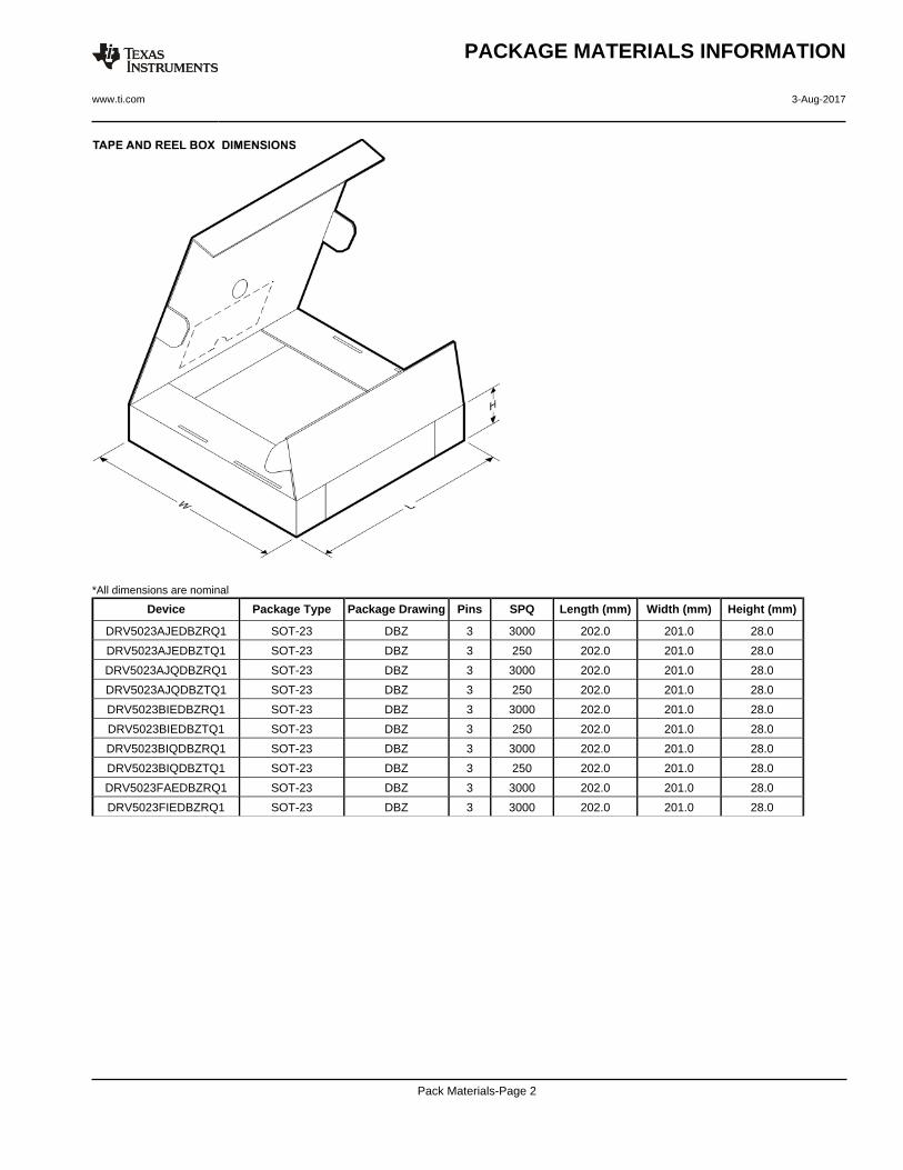
*All dimensions are nominal
Device Package Type Package Drawing Pins SPQ Length (mm) Width (mm) Height (mm)
DRV5023AJEDBZRQ1 SOT-23 DBZ 3 3000 202.0 201.0 28.0
DRV5023AJEDBZTQ1 SOT-23 DBZ 3 250 202.0 201.0 28.0
DRV5023AJQDBZRQ1 SOT-23 DBZ 3 3000 202.0 201.0 28.0
DRV5023AJQDBZTQ1 SOT-23 DBZ 3 250 202.0 201.0 28.0
DRV5023BIEDBZRQ1 SOT-23 DBZ 3 3000 202.0 201.0 28.0
DRV5023BIEDBZTQ1 SOT-23 DBZ 3 250 202.0 201.0 28.0
DRV5023BIQDBZRQ1 SOT-23 DBZ 3 3000 202.0 201.0 28.0
DRV5023BIQDBZTQ1 SOT-23 DBZ 3 250 202.0 201.0 28.0
DRV5023FAEDBZRQ1 SOT-23 DBZ 3 3000 202.0 201.0 28.0
DRV5023FIEDBZRQ1 SOT-23 DBZ 3 3000 202.0 201.0 28.0
PACKAGE MATERIALS INFORMATION
www.ti.com 3-Aug-2017
Pack Materials-Page 2

www.ti.com
PACKAGE OUTLINE
4.13.9
3X15.515.1
3X 0.480.35
2X 1.27 0.05
3.253.05
3X 0.510.36
3X 0.550.40
2X (45 )
0.860.66
1.621.42
2.642.44
2.682.28
5.05MAX
(0.5425)
3X (0.8)
4221343/C 01/2018
TO-92 - 5.05 mm max heightLPG0003ATRANSISTOR OUTLINE
NOTES: 1. All linear dimensions are in millimeters. Any dimensions in parenthesis are for reference only. Dimensioning and tolerancing per ASME Y14.5M.2. This drawing is subject to change without notice.
1 3
1 2 3
SCALE 1.300
www.ti.com
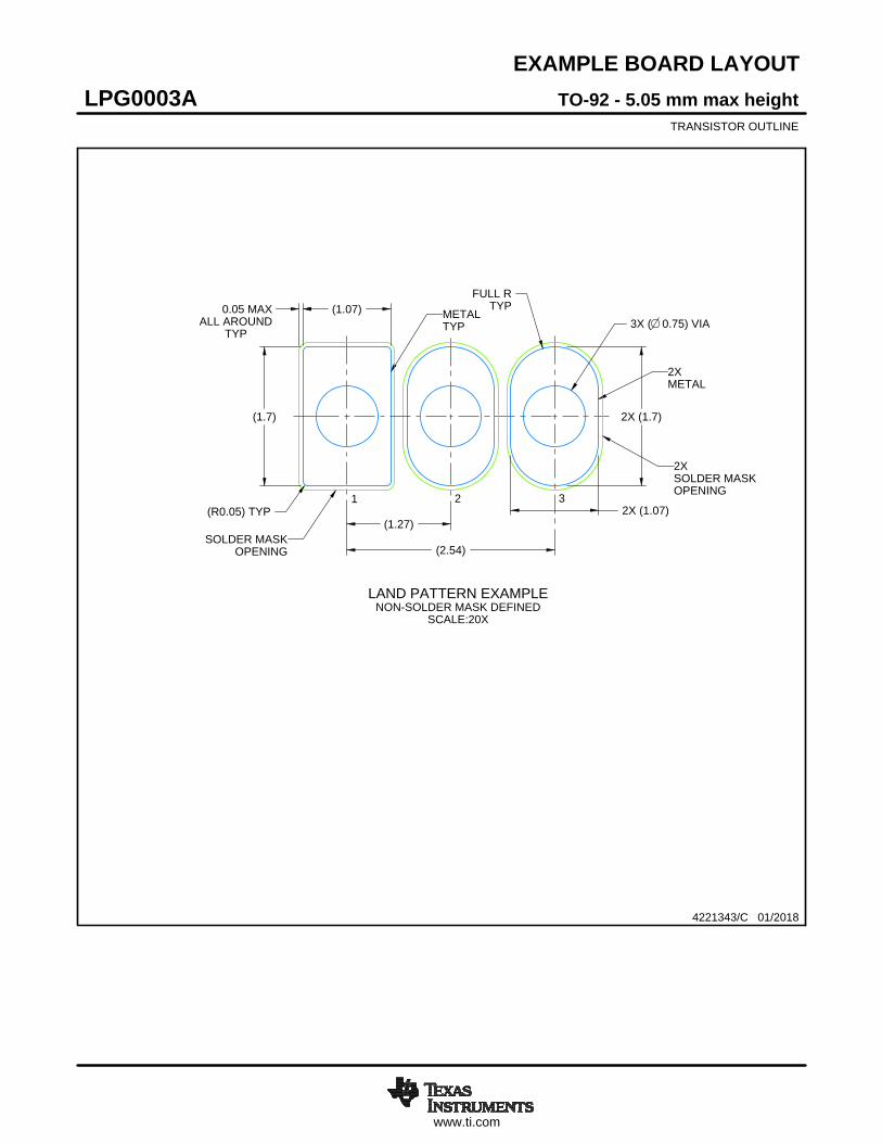
EXAMPLE BOARD LAYOUT
TYP ALL AROUND
0.05 MAXFULL R
TYP(1.07)
(1.7)
(1.27)
(2.54)
(R0.05) TYP 2X (1.07)
2X (1.7)
3X ( 0.75) VIA
4221343/C 01/2018
TO-92 - 5.05 mm max heightLPG0003ATRANSISTOR OUTLINE
LAND PATTERN EXAMPLENON-SOLDER MASK DEFINED
SCALE:20X
METALTYP
OPENINGSOLDER MASK
1 32
2XMETAL
2XSOLDER MASKOPENING
www.ti.com
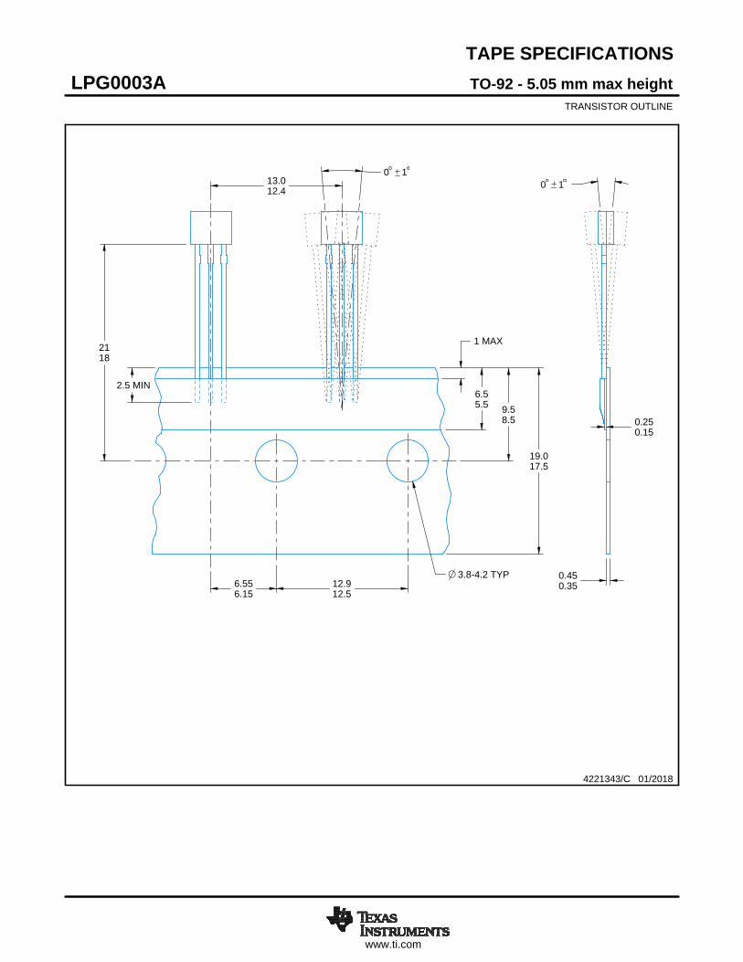
TAPE SPECIFICATIONS
0 10 1
12.912.5
6.556.15
13.012.4
2.5 MIN6.55.5
3.8-4.2 TYP
9.58.5
19.017.5
1 MAX2118
0.450.35
0.250.15
TO-92 - 5.05 mm max heightLPG0003ATRANSISTOR OUTLINE
4221343/C 01/2018
4203227/C

www.ti.com
PACKAGE OUTLINE
C
TYP0.200.08
0.25
2.642.10
1.12 MAX
TYP0.100.01
3X 0.50.3
TYP0.60.2
1.9
0.95
TYP-80
A
3.042.80
B1.41.2
(0.95)
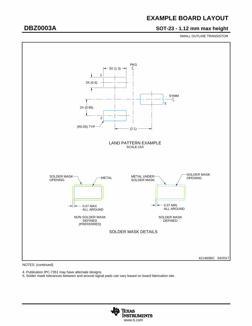
SOT-23 - 1.12 mm max heightDBZ0003ASMALL OUTLINE TRANSISTOR
4214838/C 04/2017
NOTES: 1. All linear dimensions are in millimeters. Any dimensions in parenthesis are for reference only. Dimensioning and tolerancing per ASME Y14.5M.2. This drawing is subject to change without notice.3. Reference JEDEC registration TO-236, except minimum foot length.
0.2 C A B
1
3
2
INDEX AREAPIN 1
GAGE PLANE
SEATING PLANE
0.1 C
SCALE 4.000
www.ti.com
EXAMPLE BOARD LAYOUT
0.07 MAXALL AROUND
0.07 MINALL AROUND
3X (1.3)
3X (0.6)
(2.1)
2X (0.95)
(R0.05) TYP
4214838/C 04/2017
SOT-23 - 1.12 mm max heightDBZ0003ASMALL OUTLINE TRANSISTOR
NOTES: (continued) 4. Publication IPC-7351 may have alternate designs. 5. Solder mask tolerances between and around signal pads can vary based on board fabrication site.
SYMM
LAND PATTERN EXAMPLESCALE:15X
PKG
1
3
2
SOLDER MASKOPENINGMETAL UNDER
SOLDER MASK
SOLDER MASKDEFINED
METALSOLDER MASKOPENING
NON SOLDER MASKDEFINED
(PREFERRED)
SOLDER MASK DETAILS
www.ti.com
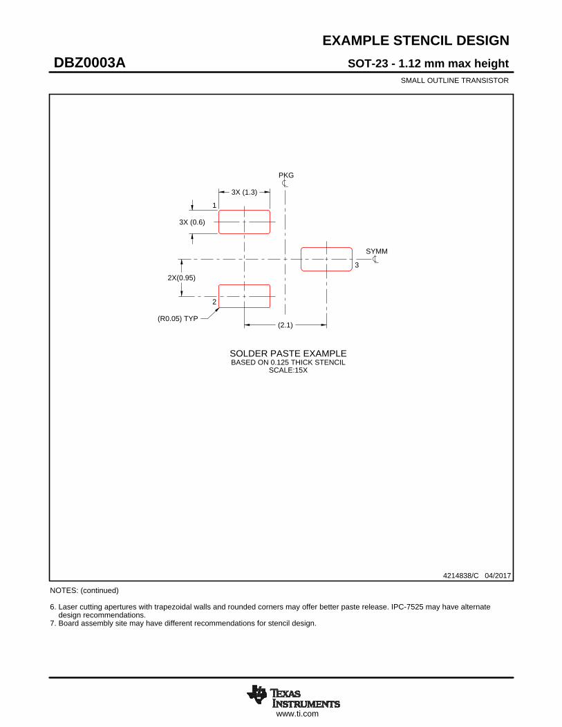
EXAMPLE STENCIL DESIGN
(2.1)
2X(0.95)
3X (1.3)
3X (0.6)
(R0.05) TYP
SOT-23 - 1.12 mm max heightDBZ0003ASMALL OUTLINE TRANSISTOR
4214838/C 04/2017
NOTES: (continued) 6. Laser cutting apertures with trapezoidal walls and rounded corners may offer better paste release. IPC-7525 may have alternate design recommendations. 7. Board assembly site may have different recommendations for stencil design.
SOLDER PASTE EXAMPLEBASED ON 0.125 THICK STENCIL
SCALE:15X
SYMM
PKG
1
3
2
IMPORTANT NOTICE
Texas Instruments Incorporated (TI) reserves the right to make corrections, enhancements, improvements and other changes to itssemiconductor products and services per JESD46, latest issue, and to discontinue any product or service per JESD48, latest issue. Buyersshould obtain the latest relevant information before placing orders and should verify that such information is current and complete.TI’s published terms of sale for semiconductor products (http://www.ti.com/sc/docs/stdterms.htm) apply to the sale of packaged integratedcircuit products that TI has qualified and released to market. Additional terms may apply to the use or sale of other types of TI products andservices.Reproduction of significant portions of TI information in TI data sheets is permissible only if reproduction is without alteration and isaccompanied by all associated warranties, conditions, limitations, and notices. TI is not responsible or liable for such reproduceddocumentation. Information of third parties may be subject to additional restrictions. Resale of TI products or services with statementsdifferent from or beyond the parameters stated by TI for that product or service voids all express and any implied warranties for theassociated TI product or service and is an unfair and deceptive business practice. TI is not responsible or liable for any such statements.Buyers and others who are developing systems that incorporate TI products (collectively, “Designers”) understand and agree that Designersremain responsible for using their independent analysis, evaluation and judgment in designing their applications and that Designers havefull and exclusive responsibility to assure the safety of Designers' applications and compliance of their applications (and of all TI productsused in or for Designers’ applications) with all applicable regulations, laws and other applicable requirements. Designer represents that, withrespect to their applications, Designer has all the necessary expertise to create and implement safeguards that (1) anticipate dangerousconsequences of failures, (2) monitor failures and their consequences, and (3) lessen the likelihood of failures that might cause harm andtake appropriate actions. Designer agrees that prior to using or distributing any applications that include TI products, Designer willthoroughly test such applications and the functionality of such TI products as used in such applications.TI’s provision of technical, application or other design advice, quality characterization, reliability data or other services or information,including, but not limited to, reference designs and materials relating to evaluation modules, (collectively, “TI Resources”) are intended toassist designers who are developing applications that incorporate TI products; by downloading, accessing or using TI Resources in anyway, Designer (individually or, if Designer is acting on behalf of a company, Designer’s company) agrees to use any particular TI Resourcesolely for this purpose and subject to the terms of this Notice.TI’s provision of TI Resources does not expand or otherwise alter TI’s applicable published warranties or warranty disclaimers for TIproducts, and no additional obligations or liabilities arise from TI providing such TI Resources. TI reserves the right to make corrections,enhancements, improvements and other changes to its TI Resources. TI has not conducted any testing other than that specificallydescribed in the published documentation for a particular TI Resource.Designer is authorized to use, copy and modify any individual TI Resource only in connection with the development of applications thatinclude the TI product(s) identified in such TI Resource. NO OTHER LICENSE, EXPRESS OR IMPLIED, BY ESTOPPEL OR OTHERWISETO ANY OTHER TI INTELLECTUAL PROPERTY RIGHT, AND NO LICENSE TO ANY TECHNOLOGY OR INTELLECTUAL PROPERTYRIGHT OF TI OR ANY THIRD PARTY IS GRANTED HEREIN, including but not limited to any patent right, copyright, mask work right, orother intellectual property right relating to any combination, machine, or process in which TI products or services are used. Informationregarding or referencing third-party products or services does not constitute a license to use such products or services, or a warranty orendorsement thereof. Use of TI Resources may require a license from a third party under the patents or other intellectual property of thethird party, or a license from TI under the patents or other intellectual property of TI.TI RESOURCES ARE PROVIDED “AS IS” AND WITH ALL FAULTS. TI DISCLAIMS ALL OTHER WARRANTIES ORREPRESENTATIONS, EXPRESS OR IMPLIED, REGARDING RESOURCES OR USE THEREOF, INCLUDING BUT NOT LIMITED TOACCURACY OR COMPLETENESS, TITLE, ANY EPIDEMIC FAILURE WARRANTY AND ANY IMPLIED WARRANTIES OFMERCHANTABILITY, FITNESS FOR A PARTICULAR PURPOSE, AND NON-INFRINGEMENT OF ANY THIRD PARTY INTELLECTUALPROPERTY RIGHTS. TI SHALL NOT BE LIABLE FOR AND SHALL NOT DEFEND OR INDEMNIFY DESIGNER AGAINST ANY CLAIM,INCLUDING BUT NOT LIMITED TO ANY INFRINGEMENT CLAIM THAT RELATES TO OR IS BASED ON ANY COMBINATION OFPRODUCTS EVEN IF DESCRIBED IN TI RESOURCES OR OTHERWISE. IN NO EVENT SHALL TI BE LIABLE FOR ANY ACTUAL,DIRECT, SPECIAL, COLLATERAL, INDIRECT, PUNITIVE, INCIDENTAL, CONSEQUENTIAL OR EXEMPLARY DAMAGES INCONNECTION WITH OR ARISING OUT OF TI RESOURCES OR USE THEREOF, AND REGARDLESS OF WHETHER TI HAS BEENADVISED OF THE POSSIBILITY OF SUCH DAMAGES.Unless TI has explicitly designated an individual product as meeting the requirements of a particular industry standard (e.g., ISO/TS 16949and ISO 26262), TI is not responsible for any failure to meet such industry standard requirements.Where TI specifically promotes products as facilitating functional safety or as compliant with industry functional safety standards, suchproducts are intended to help enable customers to design and create their own applications that meet applicable functional safety standardsand requirements. Using products in an application does not by itself establish any safety features in the application. Designers mustensure compliance with safety-related requirements and standards applicable to their applications. Designer may not use any TI products inlife-critical medical equipment unless authorized officers of the parties have executed a special contract specifically governing such use.Life-critical medical equipment is medical equipment where failure of such equipment would cause serious bodily injury or death (e.g., lifesupport, pacemakers, defibrillators, heart pumps, neurostimulators, and implantables). Such equipment includes, without limitation, allmedical devices identified by the U.S. Food and Drug Administration as Class III devices and equivalent classifications outside the U.S.TI may expressly designate certain products as completing a particular qualification (e.g., Q100, Military Grade, or Enhanced Product).Designers agree that it has the necessary expertise to select the product with the appropriate qualification designation for their applicationsand that proper product selection is at Designers’ own risk. Designers are solely responsible for compliance with all legal and regulatoryrequirements in connection with such selection.Designer will fully indemnify TI and its representatives against any damages, costs, losses, and/or liabilities arising out of Designer’s non-compliance with the terms and provisions of this Notice.
Mailing Address: Texas Instruments, Post Office Box 655303, Dallas, Texas 75265Copyright © 2018, Texas Instruments Incorporated