electrostatic mechanism of nucleation and growth of metal
TRANSCRIPT
28 SMT Magazine • February 2015
abstractMetal whiskers can grow across leads of
electric equipment causing short circuits, arc-ing, and raising significant reliability issues. The nature of metal whiskers remains a mystery after several decades of research. Here, their existence is attributed to the energy gain due to electrostatic polarization of metal filaments in the electric field induced by a metal surface. The field is induced by surface imperfections: contaminations, oxide states, grain boundaries, etc. This theory provides closed form expres-sions and quantitative estimates for the whisker nucleation and growth rates, explains whisker
by V. G. KarpovDepArTMenT OF pHYSiCS AnD ASTrOnOMY, univerSiTY OF TOleDO
Electrostatic Mechanism of Nucleation and Growth of Metal Whiskers
parameters and predicts statistical distribution of their lengths. The details of the underlying mathematical treatments have been presented in a recent publication[1] . Here, the emphasis is on a more intuitive level, and the references are omitted.
Metal whiskers are hair-like protrusions ob-served at surfaces of some metals; tin and zinc examples are illustrated in Figure 1. In spite of being omnipresent and leading to multiple failure modes in the electronics industry, the mechanism behind metal whiskers remains unknown after more than 60 years of research. While not formally proclaimed, some consen-sus, at a rather qualitative level, is that whiskers can represent a stress relief phenomenon. How-ever, that never led to any quantitative descrip-tion including order-of-magnitude estimates of whisker parameters.
Feature

30 SMT Magazine • February 2015
As a brief survey of relevant data, it should be noted that whiskers grow up to ~1–10 mm in length and vary from ~100 nm to ~30 μm in thickness. Their parameters are characterized by broad statistical distributions: side by side with fast-growing whiskers there can be oth-ers, on the same surface, whose growth is much slower or completely stalled. The metal surface conditions play a significant role. In particular, oxide structure and various contaminations are important factors determining whisker con-centration, growth rate and dimensions. The metal grain size appears to be less significant for small grains (nanometers to few microns), while whiskers are unlikely for very large grains, recrystallization can be of importance. Various additives can have significant effects on whis-ker growth, such as Pb strongly suppressing tin whiskering. Electric bias was reported to expo-nentially increase whisker growth rate, which was attributed to the effects of electric current, although other publications reported no bias ef-fect on whisker growth and even the negative effect of bias suppressed whiskering. A common observation is that whiskers grow from the root rather than from the tip, and the material re-quired for their growth is supplied from large distances through long range surface diffusion rather than from a narrow neighboring proxim-ity; there is no surrounding dent formed in the course of whisker growth.
More appealing is an informal list of ob-servations given below with the permission of its author, Dr. Gordon Davy[2]. It reflects the perspectives and the spirit of the live whisker research, shared by many in the community of Tin Whisker Group teleconferences. It has proved extremely useful for the author of this paper allowing multiple comparisons between the theory and the experiment.
• There are no “tin whisker experts.” Work-ers in the field differ only in their degree of perplexity in the face of so many inconsis-tencies.
• Nominally identical specimens may dem-onstrate drastically different densities and growth rates.
• Density may differ greatly from one region of a specimen to another; on a finer scale, there is a whisker growing here, but not there.
• Growth is at the base (i.e., the film), not the tip.
• Growth may be from the tin-substrate in-terface or from near the tin surface.
• Growth rate is often not constant. A whis-ker may stop growing for a while, then start growing again.
• Growth rate is zero at low and high tem-peratures, and seems to peak at about 25–50°C.
eLeCTrOSTaTIC MeCHaNISM OF NuCLeaTION aNd GrOWTH OF MeTaL WHISKerS continues
Feature
Figure 1: SeM pictures of tin (left) and zinc (right) whiskers (courtesy of the nASA electronic parts and packaging [nepp] program).

February 2015 • SMT Magazine 31
eLeCTrOSTaTIC MeCHaNISM OF NuCLeaTION aNd GrOWTH OF MeTaL WHISKerS continues
Feature
• Growth can be promoted by thermal cy-cling.
• Growth rate is zero below a threshold film thickness and approaches zero for high film thickness. It appears to be zero for bulk tin.
• For sputtered films, the growth rate ap-pears to be a minimum for near-zero resid-ual stress, and greater for tensile as well as compressive stress.
• Growth rate is somewhat higher at high humidity.
• Growth rate seems to be higher from fine-grained microstructure.
• Growth rate can be increased by some kinds of residues on the surface.
• Most metals dissolved in tin appear to in-crease growth rate. The one exception is Pb. The mechanism may have to do with altering the grain structure to equiaxed (from columnar).
• I do not recall hearing of the effect of small amounts of Pb (~1%) in Sn for vapor-de-posited films, or even for very thin electro-plated films.
• Distribution of thickness and length are log-normal.
• There appears to be no correlation between thickness and length.
• Median thickness is about 3 μm.• Longest whisker reported: ~25 mm.• Thinnest and thickest whiskers reported:
~100 nm, ~20 μm.• Various growth morphologies: needle-like,
odd-shaped eruptions, occasional branch-es, and there may longitudinal or circum-ferential striations. Acicular (needle-like) whiskers may be bent or kinked, and may not have the same thickness along the en-tire length.
• Long whiskers are in constant motion in air—can be compared to Brownian mo-tion.
• Whiskers have an oxide coating ~1–3 nm thick, even in vacuum. (Growth rate is log-arithmic.)
• A whisker that melts exits the skin, leaving it behind.
• Whiskers penetrate even a thick oxide film (grown by prolonged exposure to steam).
• Whiskers eventually penetrate polymer (including Parylene) coatings, with the ap-parent exception of “whisker-tough.”
• Whiskers appear to not penetrate thin caps of certain metals, and readily penetrate thicker caps of other metals.
• Whiskers appear to not penetrate thin films of tailored ceramics produced by chemical vapor deposition if the substrate has been properly prepped.
To emphasize the most challenging ques-tions, here is the author’s short list:
• A mystery of high aspect ratios, height/diameter up to ~10,000 not seen in other physics. Why wouldn’t metal whiskers col-lapse into spheres, as other droplets do to minimize surface energy?
• Is their relation to metals of essence? In other words, why are metal whiskers met-al?
• What is behind the metal whiskers ran-domness? Why do they grow here but not there, why are their parameters so dis-persed, and what makes it so difficult to controllably grow or predict their appear-ance?
• What does Pb do in suppressing whiskers?
Multiple attempts to understand the mecha-nisms of whiskers growth revolved around the role of surface stresses relived by whisker pro-duction, dislocation effects, oxygen reactions, and recrystallization. It was shown stress gradi-ents along with certain assumptions about sys-tem parameters can explain tin whisker growth rates but not their existence, shapes and sta-tistics. Overall, these attempts have not led to verifiable quantitative predictions.
The 60-year old whisker challenge thus re-mains outstanding against the background of other historical developments in natural sci-ences. As an example, the fundamentally new phenomenon of superconductivity was discov-ered in 1911 and explained in 1957, taking a shorter time to understand than metal whiskers, in spite of being the first encounter of the mac-roscopic quantum phenomena physics. This remarkable elusiveness of the metal whisker

32 SMT Magazine • February 2015
problem warrants new theoretical approaches. They need to be made quantitative in order to allow experimental verifications and satisfy the standard scientific criteria.
This paper discusses one such approach based on the electrostatics of metal surfaces. It may appear rather contradictory in the light of a common perception (taught in the under-graduate physics) that neutral metal surfaces cannot have electric charges or fields. We will see however that the latter is true only for ideal metal surfaces (containing no imperfections, such as grain boundaries, contamination, dis-locations, etc.), and that real metal surfaces can present rich electrostatics including strong elec-tric fields significantly varying across the sur-face. A theory of metal whiskers presented here is consistent with many published observations and provides some quantitative analytical re-sults. The appearance of whiskers is described as the electric field induced nucleation of needle-shaped particles. It is triggered by the energy gain FE=−p⋅E due to the induced whisker dipole p=αE in the electric field E, where α is the po-larizability. The latter is anomalously strong for the needle geometry. The nucleated whiskers continue growing to further decrease their en-ergies in the electric field.
1. More specifically, the theory is based on the concept of strong electric fields, E≤0.01-1 MV/cm, in the sub-micron proximity of metal surfaces. Such fields can be generated by surface imperfections including “wrong” grain orien-tations, deformations, oxides, dislocations, or contamination. The importance of this con-cept is that it offers a unique pattern consistent
with the observed wide variety of factors, in the first glance unrelated to each other, all having strong effects on whisker growth: stresses of me-chanical and electric nature, material morphol-ogy and composition, surface contaminations, including the effects of humidity. According to that concept, all these factors are responsible for significant electric fields in the near surface region of a metal. The surface electric field be-comes a common denominator of whisker driv-ing forces. This new hypothesis remains to be carefully tested against all the available data and focused experiments including purposely created electric fields.
2. Being overall neutral these metal surfaces are composed of oppositely charged patches formed as a result of electron redistribution minimizing the system free energy. The patches are characterized by certain surface charge den-sity and dimensions L~1−10 μm, maybe even shorter, ~0.1 mm, for fine crystalline grain struc-ture. These patches form a sort of random chess board as shown in the right display of Figure 2.
3. The phenomenon of whisker nucleation and growth is attributed to the electrostatic en-ergy gain due to strong polarization of the new-ly created needle-shaped metal particles. The conception of whiskers is described based on the (earlier developed) theory of field induced nucleation that predicts needle-shaped embry-os h≤100 nm in length and d~1–10 nm in di-ameter. The mechanism is quite similar to that explaining the fact that amber or plastic comb attract small pieces of paper: The electric field polarized small particles making them electric
eLeCTrOSTaTIC MeCHaNISM OF NuCLeaTION aNd GrOWTH OF MeTaL WHISKerS continues
Feature
Figure 2: A sketch of the electric field e near a metal surface, cross-sectional (left) and 3D (right) views.
34 SMT Magazine • February 2015
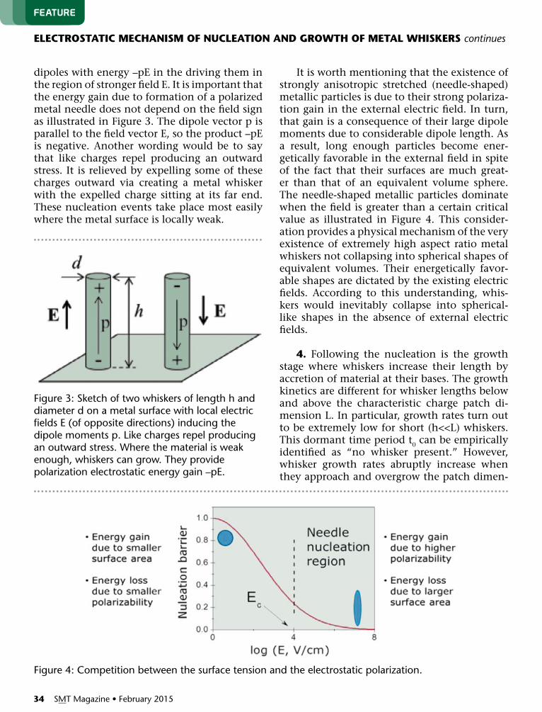
dipoles with energy –pE in the driving them in the region of stronger field E. It is important that the energy gain due to formation of a polarized metal needle does not depend on the field sign as illustrated in Figure 3. The dipole vector p is parallel to the field vector E, so the product –pE is negative. Another wording would be to say that like charges repel producing an outward stress. It is relieved by expelling some of these charges outward via creating a metal whisker with the expelled charge sitting at its far end. These nucleation events take place most easily where the metal surface is locally weak.
eLeCTrOSTaTIC MeCHaNISM OF NuCLeaTION aNd GrOWTH OF MeTaL WHISKerS continues
Feature
It is worth mentioning that the existence of strongly anisotropic stretched (needle-shaped) metallic particles is due to their strong polariza-tion gain in the external electric field. In turn, that gain is a consequence of their large dipole moments due to considerable dipole length. As a result, long enough particles become ener-getically favorable in the external field in spite of the fact that their surfaces are much great-er than that of an equivalent volume sphere. The needle-shaped metallic particles dominate when the field is greater than a certain critical value as illustrated in Figure 4. This consider-ation provides a physical mechanism of the very existence of extremely high aspect ratio metal whiskers not collapsing into spherical shapes of equivalent volumes. Their energetically favor-able shapes are dictated by the existing electric fields. According to this understanding, whis-kers would inevitably collapse into spherical-like shapes in the absence of external electric fields.
4. Following the nucleation is the growth stage where whiskers increase their length by accretion of material at their bases. The growth kinetics are different for whisker lengths below and above the characteristic charge patch di-mension L. In particular, growth rates turn out to be extremely low for short (h<<L) whiskers. This dormant time period t0 can be empirically identified as “no whisker present.” However, whisker growth rates abruptly increase when they approach and overgrow the patch dimen-
Figure 3: Sketch of two whiskers of length h and diameter d on a metal surface with local electric fields e (of opposite directions) inducing the dipole moments p. like charges repel producing an outward stress. Where the material is weak enough, whiskers can grow. They provide polarization electrostatic energy gain –pe.
Figure 4: competition between the surface tension and the electrostatic polarization.

February 2015 • SMT Magazine 35
sion L, after which the growth rate remains on average constant. The physical reason of that acceleration is that the longer the whisker the stronger the electrostatic energy gain and its corresponding thermodynamic force pulling the whisker. This process can be explosive (posi-tive feedback) in nature: The stronger the force, the faster the growth, the greater the length, and the stronger the force, etc., as long as the force increases with length (for h<L when the field is more or less uniform). However, in the range of h>>L, the field appears strongly fluctu-ating (Figure 2) which significantly suppresses the pulling force. As a result, the pulling force becomes independent of whisker length (Figure 5). That distant independent average force re-sults in constant average growth rates.
The predicted time dependent growth rate is sketched in Figure 6. The dormant time t0 cor-responds to whisker development over short
distances h<L. As explained in the preceding paragraph, growth accelerates as h–>L. For the overgrown whiskers with h>>L, the growth rate becomes time independent on average.
5. The latter statement of constant growth rate for whisker lengths h>>L holds true on av-erage. In reality, a whisker encounters a random distribution of fields in the course of its growth as can be realized from Figure 4. A whisker head passes through multiple regions of various direc-tions and strengths. Correspondingly, the whis-ker length growth rate fluctuates between low and high values. It can be shown that the most significant electrostatic energy gain is achieved via the increase of whisker length rather than the diameter. Therefore, when the material sup-ply is limited, the energy gain will dictate that whiskers grow in length as much as possible. However, when the length growth is suppressed
Figure 5: Top left: free energy vs. whisker length h where the downhill slope corresponds to the growth stage of whiskers; W is the nucleation barrier, h0 is the critical nucleation dimension of the needle-shaped embryo. The shape of that slope is determined by the charged patch model shown to the right of the free energy plot where r is the distance from a metal surface and l is the characteristic patch dimension. bottom: the free energy vs. whisker length with the marked regions of qualitatively different dependencies.
eLeCTrOSTaTIC MeCHaNISM OF NuCLeaTION aNd GrOWTH OF MeTaL WHISKerS continues
Feature

36 SMT Magazine • February 2015
in some local regions, the further energy gain can be achieved via the diameter increase (i.e., whiskers get thicker intermittently with the pe-riods of faster length increase). A snapshot of many such whisker lengths and diameters will therefore show broad statistical distributions that are mutually uncorrelated.
Figure 7 illustrates the process of whisker growth in a 2D fashion where the color coding is such that upward and downward local elec-tric field directions are shown in respectively red and blue. The sign fluctuations of the field at large distances shown in Figure 5 do not eliminate the polarization energy gain. Indeed, consider a long metal whisker as a succession of many small metal rods, each occupying a small range of more or less constant field. They have local dipole moments p=aE, and partial electro-static energies pE=aE2 that are quadratic in field and do not cancel each other. Taking into ac-count the explanation in Figures 3 and 5, it is intuitively clear that the maximum polarization and electrostatic energy gain are achieved for the “color-matched” whiskers (all in blue or all
in red). The corresponding pathways for whis-ker growth can be kinked in order to collect as many as possible color matched regions. This explains how whiskers can be kinked. It should be noted however that each kink entails certain deformation energy loss, so the whisker geom-etry will optimize between the gain in electro-static energy and loss in deformation energy due to kinking. (These subtle features remain unaccounted quantitatively in the current elec-trostatic whisker theory.) Furthermore, some configurations of color-matched regions pres-ent pathways parallel or partially parallel to the surface; this explains the observed longitudinal or circumferential striations shown in dash in Figure 7.
6. In the course of growing at h>>L, whis-kers encounter rare local regions of abnormally low electric fields where its further growth is blocked. The blockage is due to the fact that further growth in these low field regions can-not overweigh the energy loss due to increase in surface area: the latter increase presents a signifi-
Figure 6: Sketch of the whisker growth rates vs. time. Solid lines represent the two limiting cases within the domains of their applicability (h<<l and h>>l, respectively). The dashed curves are formal solutions presented by the first and the second equations in the formula displayed above. The dash-dotted line shows a hypothetical sewing.
Figure 7: A sketch of whisker growth through a space of a fluctuating electric field:• rapid growth while either + or – fields dominate along the length.• For large lengths, + and – fields start balancing each other.• Whiskers stop growing at certain random lengths, which explains whisker statistics.• Can resume growth after a while.
eLeCTrOSTaTIC MeCHaNISM OF NuCLeaTION aNd GrOWTH OF MeTaL WHISKerS continues
Feature

38 SMT Magazine • February 2015
cant energy barrier. The statistics of these block-ing regions (barriers) determines the whisker length statistics. It is derived to be close to log-normal in the proximity of the most likely sizes, while decaying much faster for sizes well above the average. It should be emphasized however that such blocking energy barriers have finite heights WB. Therefore, they can be overcome after significant waiting times tW =t0 exp(WB / kT) allowing for sufficient number of attempt-to-escape events, each taking time t0 where kT is the thermal energy. This explains the obser-vation of whiskers resuming growth after a con-siderable time (approaching a year) of lethargy. Based on this reasoning and using the standard techniques of the physics of random systems, it is possible to derive the probabilistic distribu-tion of whisker length. Its explicit mathemati-cal form turns out to be cumbersome; however, the qualitative features are quite simple and are illustrated in Figure 9.
7. The concept of field induced nucleation and growth of metal filaments is neither unique nor very new; in a quantitative form it was put forward in the recently developed field induced nucleation theory. Here we would like to men-tion some applications of that concept concern-ing objects that may be related to metal whis-kers in their underlying physics.
Our first example is represented by the
shunting entities observed in various elec-tronic elements (mostly in semiconductor and insulator films) that are conductive filaments developed in the host of relatively insulating materials subject to electric bias. There is a con-siderable R&D activity, often in industrial set-tings, including different technologies, such as microelectronics, thin film photovoltaics, light emitting diodes, etc., in the course of which the problem is considered from different points of view, often ignoring a possibility of common mechanism based on the field induced electro-static energy gain.
Side by side with the detrimental effects of shunting, there is a strong research effort to understand possible beneficial effects of for-mation of conductive filaments under electric bias. They include, first of all, the technologies of phase change and resistive memories, where the structure states with and without the con-ductive filament are used as the two logic states of the memory element. Some illustrations are given in Figure 10.
Shown in Figure 11 are needle-like structures that appear on the surface of a liquid metal in a strong perpendicular electric field. The nature
Figure 8: in the flat portion of the electrostatic free energy Fe, the whisker surface energy Fa forms a barrier Wb in the total whisker energy F=Fa+Fe . in this diagram, W is the whisker nucleation barrier.
Figure 9: an example of the predicted probabi-listic distribution of whisker lengths vs. its best fit approximation by the log-normal distribution. note that the best fit (least square) approxima-tion provides good fit in the middle part of the distribution, while it is less successful in the re-gions of both very long and very short whiskers.
eLeCTrOSTaTIC MeCHaNISM OF NuCLeaTION aNd GrOWTH OF MeTaL WHISKerS continues
Feature

February 2015 • SMT Magazine 39
of such needles remains obscure, although the shape of their pedestals is explained as the so-called Taylor cones representing an equilibrium (between the electrostatic polarization and the surface tension) geometry of a metal surface. From the perspectives of this paper’s philoso-phy, these needles, metal whiskers, and those responsible for shunting and solid state mem-ory features are all mutually related due to the electrostatic energy gain.
8. Because of its counterintuitive nature, the discussion about strong electric fields in the near surface regions of real metals may require further comment. These fields can arise from spatial variations of the work function depend-ing on multiple imperfections in structure and composition. At the first glance, the existence of such fields may appear contradictory. Indeed, free electrons in metals have a tendency to screen electric charge fluctuations, thereby sup-pressing electric fields. However, as explained in the next section, the role of free electrons is exact opposite. Their ability to move underlies the electric charge variations.
To avoid any misunderstanding, it is not the condition of local electroneutrality, but rather that of minimum free energy that determines the electric charge (and other parameters) dis-
tributions. The electrons will always move to minimize the system free energy; this leads to non-uniform charge distributions in non-ho-mogeneous systems. In other words, not only the existence of surface electric fields and their corresponding electric charge variations are ful-ly consistent with the concept of free electrons, but it is due to free electrons that different local regions of a metal can exchange electric charges minimizing the system free energy. It is widely known in the physics of semiconductors (but has not been applied to metals often) that it is not the electric potential j, but rather the elec-
Figure 11: Structures pulled up by a strong electric field on the surface of a molten metal[3].
Figure 10: illustrations of the electric field induced conductive filaments in resistive memory devices.
eLeCTrOSTaTIC MeCHaNISM OF NuCLeaTION aNd GrOWTH OF MeTaL WHISKerS continues
Feature

40 SMT Magazine • February 2015
trochemical potential F = m + ej that needs to be constant in space in order to minimize the sys-tem free energy. Here, m is the chemical poten-tial (change in the system energy in response to the change of number of particles in it by one; the difference in chemical potentials between two substances equals minus that of the corre-sponding work functions). The chemical poten-tial is sensitive to all kind of chemical features, deformations, defects, etc. Figure 12 shows how the concentrations of particles n are significantly different in the two regions with different chem-ical potentials. As a result, the particles move to the region of lower chemical potential. Because of the accumulated electric charge, there is now electric field E in the system. However, its cor-responding drift current nEb (b is the mobility) is totally balanced by the diffusion current Ddn/dx, where D is the diffusion coefficient and x is the coordinate in the direction of concentration gradient. The important conclusion is that it is a metal where there is no current while the elec-tric field is not vanishing.
It follows from the latter that some struc-tural or compositional inhomogeneities are needed for the electric charge redistribution triggering whisker growth. Grain structure can be one (but not the only) example of such inho-mogeneities. This is consistent with the general observation that whiskers are unlikely on metal surfaces built of very large grains, and that the
presence of grain boundaries can be essential. Before pointing at more specific factors behind electric field variations, the following general examples (i–iii) are aimed at illustrating the un-derlying physics.
i. Consider local stresses (due to grain bound-aries, dislocations, or external loads) modulat-ing interatomic distances in a metal, thus mak-ing some local regions denser than the others.
Because of these local variations, some re-gions will present deeper potential wells for the electrons (a phenomenon known as the defor-mation potential D = dm / du 1 eV where u is the dilation). Should these regions be mutually independent, the Fermi level positions would vary between them. However, because they are connected, the free electrons will move to level out the Fermi level across the entire system thus minimizing the system free energy. As a result, the above regions become electrically charged.
ii. Spatial variations in chemical composi-tion of alloys would similarly result in modula-tions of work function, which will be leveled out in the course of electron redistribution cre-ating local electric fields similar to the previous example.
iii. The extreme case of the latter is present-ed by a contact of different metals with unequal
Figure 12: a sketch of a spatial distribution of the electric potential including two regions with the relative-ly low (left) and relatively high (right) chemical potential m. To utilize that difference in chemical poten-tials, the electrons partially moved from right to left creating non-uniform electric charge distribution and its corresponding non-uniform electric potential j and electric field e. The quantity that remains constant throughout the region is the electro-chemical potential F = m + ej where e is the electron charge.
eLeCTrOSTaTIC MeCHaNISM OF NuCLeaTION aNd GrOWTH OF MeTaL WHISKerS continues
Feature
42 SMT Magazine • February 2015
work functions. The free electrons will move between these metals to equalize their Fer-mi levels. This makes the metals electrically charged. The same phenomenon underlies the existence of Schottky barriers and p-n junctions in semiconductors. In the case of metal cou-ples, it is known as the source of the galvanic action that occurs when two electrochemically dissimilar metals are in contact and a conduc-tive path occurs for electrons and ions to move from one metal to the other. Furthermore, one can imagine a binary mixture of chemically dif-ferent metal grains where the balance of Fermi energy makes the grains of two types charged oppositely.
The above cases (i) and (ii) are schematically illustrated in Figure 13.
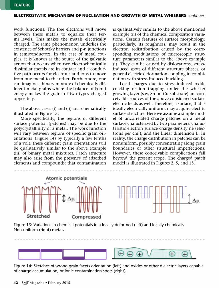
More specifically, the regions of different surface potential (patches) may be due to the polycrystallinity of a metal. The work function will vary between regions of specific grain ori-entations (Figure 14) by typically a few tenths of a volt; these different grain orientations will be qualitatively similar to the above example (iii) of binary metal mixtures. Patch structure may also arise from the presence of adsorbed elements and compounds; that contamination
is qualitatively similar to the above mentioned example (ii) of the chemical composition varia-tions. Certain features of surface morphology, particularly, its roughness, may result in the electron redistribution caused by the corre-sponding modulations of microscopic struc-ture parameters similar to the above example (i). They can be caused by dislocations, stress-induced spots of different structure phases, or general electric deformation coupling in combi-nation with stress-induced buckling.
Local charges due to stress-induced oxide cracking or ion trapping under the whisker growing layer (say, Sn on Cu substrate) are con-ceivable sources of the above considered surface electric fields as well. Therefore, a surface, that is ideally electrically uniform, may acquire electric surface structure. Here we assume a simple mod-el of uncorrelated charge patches on a metal surface characterized by two parameters: charac-teristic electron surface charge density ne (elec-trons per cm2), and the linear dimension L. In reality, the charge distribution in patches can be nonuniform, possibly concentrating along grain boundaries or other structural imperfections. However, these conceivable complications fall beyond the present scope. The charged patch model is illustrated in Figures 2, 5, and 15.
Figure 13: variations in chemical potentials in a locally deformed (left) and locally chemically non-uniform (right) metals.
Figure 14: Sketches of wrong grain facets orientation (left) and oxides or other dielectric layers capable of charge accumulation, or ionic contamination spots (right).
eLeCTrOSTaTIC MeCHaNISM OF NuCLeaTION aNd GrOWTH OF MeTaL WHISKerS continues
Feature

February 2015 • SMT Magazine 43
Patch structured electric fields near metal surfaces have been found in multiple works. The measurements reveal the work function fluctua-tions of ~0.5 eV induced by L~10 μm patches in some metals.
The charged patch model enables one to estimate the average electric field vs. distance r from the surface. At distances r<<L, the field is close to uniform due to the dominance of the closest uniformly charged patch. At distances r>>L, fluctuations become essential and the av-erage field amplitude decays inversely propor-tional to r. In addition, given the above model, it is straightforward to see that far from the sur-face, r>>L, the electric field vectors are directed on average perpendicular to the surface having a considerable dispersion in angles,
equation 1
where E^ and E|| are respectively the field components perpendicular and parallel to the surface, and angular brackets represent averag-ing.
9. The above estimates lead to the follow-ing scenario of whisker evolution. (i) Stage 1: Whiskers nucleate in time intervals of one sub-second to one day (reflecting fluctuations in nucleation barriers due to the local field fluc-tuations); their dimensions upon nucleation are h~10–100 nm and d~1–10 nm, with the average orientation perpendicular to the metal surface and significant angular dispersion. (ii) Stage 2: Whiskers grow up to the patch size, say L~0.1–10 μm. This takes a much longer time t0~104–105 that can be experimentally identified as the whisker incubation time. The growth rate at this stage is very low for almost entire time interval t0, with drastic acceleration in the nearest proximity of t0 (see Figure 6). (iii) Stage 3: Whiskers grow way above patch size at the average constant rate possibly with some degree of winding or kinking (beyond the current theory). At this stage, random field configurations induced by uncorrelated patch charges make growth rates of individual whis-kers fluctuating, some of them blocked. The random distribution of blocking barriers de-termines the statistical distribution of whisker lengths. (iv) Stage 4: If whiskers grow above lengths where feeding by thermal radiation dominates, they evolve further in lateral di-rections parallel to the metal surface (not dis-cussed here).
Figure 15: Charged patch model. The correlation function g(x) can be approximated as the delta-function (i.e., uncorrelated disorder) at distances x>>l.
eLeCTrOSTaTIC MeCHaNISM OF NuCLeaTION aNd GrOWTH OF MeTaL WHISKerS continues
Feature

44 SMT Magazine • February 2015
10. ConclusionsThe above theory describes metal whickers as
a result of metal nucleation and growth in ran-dom electric fields induced by charged patches on metal surfaces. The underlying approaches are typical of the physics of phase transitions and disordered systems. This work presents the first whisker theory yielding simple analytical results more or less consistent with the observa-tions. The successes, the remaining questions, and possible experimental verifications of this theory are summarized next.
10.1 What is understood1) Why whiskers are metallic: High (metal-
lic) electric polarizability is required for suffi-cient energy gain due to whisker formation in external (surface) electric fields.
2) Why whiskers grow more or less perpen-dicular to the surface and yet can have con-figurations parallel to the surface: Such are the dominating directions of the surface electric field that include significant fluctuation along the surface.
3) Why whisker parameters are broadly sta-tistically distributed: This reflects fluctuations in metal surface fields induced by mutually un-correlated charged patches.
4) Correlation between whiskers and ver-satile morphology factors, such as (i) grains whose orientation is different from the major orientation of the tin film, (ii) dislocations and dislocation loops, and (iii) mechanical stresses capable of surface buckling, surface contami-nations; all related to local surface charges and their induced electric fields. Some metals are more prone to develop whiskers because they can easier form charged patches by absorbing ions, and creating dislocations, grain boundar-ies, or stresses.
5) Why external electric bias can significant-ly affect whisker growth. (It is rather difficult, yet possible, beyond this paper framework, to understand how the electric bias can be not a significant factor in whisker kinetics.)
6) Why the characteristic whisker evolution exhibits a certain pattern: long incubation pe-riod followed by almost constant growth rate that eventually saturates. The predicted incu-bation (dormant) time and subsequent growth
rate agree with the observations.7) Why whisker parameters are broadly dis-
tributed statistically. The predicted distribution of whisker lengths is close to the observed log-normal statistics around its central part.
10.2 What is not understood1) The microscopic nature of whiskers, their
correlation with specific surface defects, chemi-cal aspects of whisker development.
2) The role of whisker crystalline structure in their evolution process.
3) Whisker growth in 3D random electric field. This includes whisker winding and kink-ing.
4) Possible role of surface (or grain bound-ary) diffusion limiting whisker growth.
5) Possible hydrodynamic drag moving sur-face material uniformly along with ions.
6) Inter-whisker interactions limiting their concentration and affecting growth. This in-cludes the stage of whisker ripening.
7) Role of Pb in suppressing whiskering.
10.3 Possible experimental verificationThe predicted dependencies of nucleation
and growth kinetics vs. electric field, tempera-ture, and controlled contamination could be verified experimentally.
1) Whisker nucleation and growth in exter-nal electric fields. This can be attempted, e.g., in flat plate capacitor configuration for a whis-ker inside SEM where the electric field is readily controlled, or under e-beam in an accelerator. In all cases, care should be taken to avoid signif-icant Joule heating and/or electron drag effects (i.e., using voltage rather than current power source). An ongoing project in our group has generated preliminary results showing that the electric field in combination with high relative humidity can lead to anomalously rapid whis-ker growth (one week under 3000 V/cm in a capacitive configuration; 10–20 hours of medi-cal accelerator e-beam charging a glass substrate under Sn film).
2) Whisker nucleation and growth under controlled contamination of metal surface with solutions of charged nano particles.
3) Whisker nucleation and growth under the conditions of strong surface electric fields
eLeCTrOSTaTIC MeCHaNISM OF NuCLeaTION aNd GrOWTH OF MeTaL WHISKerS continues
Feature

February 2015 • SMT Magazine 45
induced by surface plasmon polariton excita-tions. This technique could be used for con-trolled growth of metal nanowires of desirable parameters on metal surfaces.
4) Applications to modern large area thin film photovoltaic technology where whiskers can shunt through the device, thereby causing significant reliability concerns (which has not been sufficiently addressed yet). Properly re-placing those device metal contacts or surface treatments mitigating whisker growth can im-prove the device reliability and stability with respect to shunting.
acknowledgementThe author is grateful to D. Shvydka, A.
Vasko, G. Davy, S. Smith, B. Rollins, J. Brusse, A. Kostic, and the entire tin whisker teleconfer-ence group for useful discussions. The NASA
Electronic Parts and Packaging (NEPP) Program is greatly appreciated. SMT
references1. V. G. Karpov, Electrostatic Theory of Met-
al Whiskers, Physical Review Applied, 1, 044001 (2014).
2. Private communication, October 2014, slightly abridged here.
3. G. A. Mesyats, Explosive Electron Emis-sion, URO Press, Ekaterinburg, (1998); p.29
Victor Karpov is professor of physics at the university of Toledo. He has published about 200 papers on condensed mat-ter, physical chemistry, photovol-taics, and device physics.
eLeCTrOSTaTIC MeCHaNISM OF NuCLeaTION aNd GrOWTH OF MeTaL WHISKerS continues
rice university scientists advanced their recent development of laser-induced graphene (lig) by producing and testing stacked, three-dimensional supercapacitors, energy-storage devices that are im-portant for portable, flexible electronics.
The rice lab of chemist James Tour discovered last year that firing a laser at an inexpensive poly-mer burned off other elements and left a film of po-rous graphene, the much-studied atom-thick lattice of carbon. The researchers viewed the porous, con-ductive material as a perfect electrode for superca-pacitors or electronic circuits.
Members of the Tour group have since extended their work to make vertically aligned supercapacitors with laser-induced graphene on both sides of a poly-mer sheet. The sections are then stacked with solid electrolytes in between for a multi-layer sandwich with multiple microsu-percapacitors.
The flexible stacks show excellent energy-storage capacity and power potential and can be scaled up for commercial applications. liG can be made in air at ambient temperature,
perhaps in industrial quantities through roll-to-roll processes, Tour said.
The research was reported this week in applied Materials and interfaces.
liG supercapacitors appear able to do everything capacitors can do, with the added benefits of flex-ibility and scalability. The flexibility ensures they can easily conform to varied packages—they can be rolled within a cylinder, for instance—without giving up any of the device’s performance.
“What we’ve made are comparable to microsu-percapacitors being commercialized now, but our ability to put devices into a 3-D configuration allows us to pack a lot of them into a very small area,” Tour said. “We simply stack them up.
“The other key is that we’re doing this very sim-ply. nothing about the process requires a clean room. it’s done on a commercial laser system, as found in routine machine shops, in the open air.”
ripples, wrinkles and sub-10-nanometer pores in the surface and atomic-level imperfections give
liG its ability to store a lot of energy. but the graphene retains its ability to move electrons quickly and gives it the quick charge-and-release characteris-tics of a supercapacitor. in testing, the researchers charged and discharged the devices for thousands of cycles with almost no loss of capacitance.
Laser-induced Graphene Vital for Flex Electronics
Feature