fabrication and optimization of a nanoplasmonic chip for
TRANSCRIPT
UMEÅ UNIVERSITY
MASTER’S THESIS
Fabrication and Optimization of aNanoplasmonic Chip for Diagnostics
Author:Jonas SEGERVALD
Supervisor:Dr. Xueen JIA
Examiner:Prof. Thomas WÅGBERG
A thesis submitted in fulfillment of the requirementsfor the degree of Master’s of Science in Engineering Physics
in the
Nano For Energy GroupUmeå University
October 11, 2019
© 2019 JONAS SEGERVALD


iii
“The important thing is not to stop questioning. Curiosity has its own reason for existence.One cannot help but be in awe when he contemplates the mysteries of eternity, of life, of themarvelous structure of reality. It is enough if one tries merely to comprehend a little of thismystery each day.”
Albert Einstein

v
UMEÅ UNIVERSITY
AbstractFaculty of Science and Technology
Nano For Energy Group
Master’s of Science in Engineering Physics
Fabrication and Optimization of a Nanoplasmonic Chip for Diagnostics
by Jonas SEGERVALD
To increase the survival rate from infectious- and noncommunicable diseases, reli-able diagnostic during the preliminary stages of a disease onset is of vital impor-tance. This is not trivial to achieve, a highly sensitive and selective detection systemis needed for measuring the low concentrations of biomarkers available. One possi-ble route to achieve this is through biosensing based on plasmonic nanostructures,which during the last decade have demonstrated impressive diagnostic capabilities.These nanoplasmonic surfaces have the ability to significantly enhance fluorescenceand Raman signals through localized hotspots, where a stronger then normal electricfield is present. By further utilizing a periodic sub-wavelength nanohole array theextraordinary optical transmission phenomena is supported, which open up newways for miniaturization.
In this study a nanoplasmonic chip (NPC) composed of a nanohole array —withlateral size on the order of hundreds of nanometer— covered in a thin layer of goldis created. The nanohole array is fabricated using soft nanoimprint lithography ontwo resists, hydroxypropyl cellulose (HPC) and polymethyl methacrylate (PMMA).An in depth analysis of the effect of thickness is done, where the transmittance andRaman scattering (using rhodamine 6G) are measured for varying gold layers from5 to 21 nm. The thickness was proved to be of great importance for optimizing theRaman enhancement, where a maximum was found at 13 nm. The nanohole arraywere also in general found beneficial for additionally enhancing the Raman signal.A transmittance minima and maxima were found in the region 200-1000 nm for theNPCs, where the minima redshifted as the thickness increased. The extraordinarytransmission phenomena was however not observed at these thin gold layers. Oxy-gen plasma treatment further proved an effective treatment method to reduce thehydrophobic properties of the NPCs. Care needs be taken when using thin layersof gold with a PMMA base, as the PMMA structure could get severely damaged bythe plasma. HPC also proved inadequate for this projects purpose, as water-basedfluids easily damaged the surface despite a deposited gold layer on top.


vii
AcknowledgementsDuring my master’s thesis work I have been given help and guidance from many ofthe employees at the Physics Department at Umeå University. This have includedeverything from operating an instrument, giving helpful tips or just general assis-tance. For this help freely given I sincerely thank you.
I would like to highlight four persons for their major contributions, without yourhelp this project would have been monumentally harder to finish.
Professor Thomas Wågberg, for his continuous support, assistance and help-ful perspectives.
Doctor Xueen Jia, for his excellent mentorship and guidance.
Doctor Nicolas Boulanger, for the many hours of teaching, analyzing and prob-lem solving that he voluntarily spent on me.
Doctoral Student Attila Simkó, for the much appreciated help with spell check-ing and editing of the actual thesis.

ix
Contents
Abstract v
Acknowledgements vii
List of Abbreviations xi
1 Introduction 1
2 Theory 32.1 Plasmon Theory . . . . . . . . . . . . . . . . . . . . . . . . . . . . . . . . 32.2 Surface Enhanced Raman Spectroscopy . . . . . . . . . . . . . . . . . . 32.3 Metal Enhanced Fluorescence . . . . . . . . . . . . . . . . . . . . . . . . 5
3 Method 73.1 Equipment & Material . . . . . . . . . . . . . . . . . . . . . . . . . . . . 8
3.1.1 Material . . . . . . . . . . . . . . . . . . . . . . . . . . . . . . . . 83.1.2 Equipment . . . . . . . . . . . . . . . . . . . . . . . . . . . . . . . 8
Spin coater . . . . . . . . . . . . . . . . . . . . . . . . . . . . . . . 8Nanoimprint lithography . . . . . . . . . . . . . . . . . . . . . . 8Physical vapor deposition . . . . . . . . . . . . . . . . . . . . . . 9Optical tensiometer . . . . . . . . . . . . . . . . . . . . . . . . . . 9Atomic force microscopy . . . . . . . . . . . . . . . . . . . . . . 9Plasma treatment system . . . . . . . . . . . . . . . . . . . . . . 11Scanning electron microscopy . . . . . . . . . . . . . . . . . . . . 11Fluorescence system . . . . . . . . . . . . . . . . . . . . . . . . . 11Raman spectroscopy . . . . . . . . . . . . . . . . . . . . . . . . . 11Spectrophotometer . . . . . . . . . . . . . . . . . . . . . . . . . . 12
3.2 Experimental Procedures . . . . . . . . . . . . . . . . . . . . . . . . . . . 133.2.1 Fabrication of a nanoplasmonic chip . . . . . . . . . . . . . . . . 13
Creation of replica molds . . . . . . . . . . . . . . . . . . . . . . 13Cleaning and preparation of microscope glass . . . . . . . . . . 13Resist preparation and thin layer deposition by spin coating . . 14Nanoimprinting lithography optimization . . . . . . . . . . . . 14Thin layer deposition - evaporation of gold . . . . . . . . . . . . 15
3.2.2 Plasma treatment optimization . . . . . . . . . . . . . . . . . . . 153.2.3 Surface enhanced Raman spectrosopy measurements . . . . . . 163.2.4 Fluorescence measurements . . . . . . . . . . . . . . . . . . . . . 163.2.5 Transmittance measurements . . . . . . . . . . . . . . . . . . . . 16
4 Results & Discussion 174.1 Nanoimprints & Replica mold . . . . . . . . . . . . . . . . . . . . . . . . 174.2 Physical Vapor Deposition & Nanoplasmonic Chip . . . . . . . . . . . 194.3 Plasma Treatment & Hydrophobic Properties . . . . . . . . . . . . . . . 22

x
4.4 Transmittance Data . . . . . . . . . . . . . . . . . . . . . . . . . . . . . . 264.5 Surface Enhanced Raman Spectroscopy &
Fluorescence Measurements . . . . . . . . . . . . . . . . . . . . . . . . . 274.6 Scaling Up - Nanoimprinting Lithography . . . . . . . . . . . . . . . . 29
5 Conclusions 315.1 Future Work . . . . . . . . . . . . . . . . . . . . . . . . . . . . . . . . . . 32
Bibliography 33

xi
List of Abbreviations
AFM Atomic Force MicroscopyCMG Cleaned Microscope GlassEM ElectromagneticEOT Extraordinary Optical TransmissionHPC Hydroxypropyl CelluloseLSP Localised Surface PlasmonLSPR Localised Surface Plasmon ResonanceMEF Metal Enhanced FluorescenceNPC Nanoplasmonic ChipNI NanoimprintedPDMS PolydimethylsiloxanePMMA Polymethyl MethacrylatePSD Photo-Sensitive DetectorPT Plasma TreatmentPVD Physical Vapor DepositionR6G Rhodamine 6GSEM Scanning Electron MicroscopySERS Surface Enhanced Raman Spectroscopy


xiii
Dedicated to my family, for their never-ending love andsupport. . .

1
Chapter 1
Introduction
According to the World Health Organizations report on world health statistics in2018, tens of millions of people die each year due to infectious- and noncommu-nicable diseases [1]. To successfully combat these mortality rates a very importantfactor is the possibility for accurate and reliable diagnostics during the preliminarystages of a disease onset [2]. Not only does this allow for curative treatment to beapplied early, it also helps to identify what specific treatment to be applied —as ex-pressed symptoms can usually be linked to more than one disease [3]. As only lowconcentrations of biomarkers are available during these preliminary stages, a highlysensitive and selective detection system needs to be developed [4]. It is also desirablefor the detection system to be portable and capable of on-site diagnostics to reach aglobal scale.
Accessible diagnostics methods on the market for infectious diseases range fromthe use of traditional techniques —such as microscopy and cell culture— to moreadvanced ones like immunoassays, DNA microarrays and nanotechnology [5]. Dur-ing the last decades biosensing have emerged as a powerful tool for diagnostics, aslabel-free and sensitive real-time detection of biomolecules and more complex enti-ties have been achieved [6]. A biosensor in its simplest form has two parts, a biore-ceptor which acts to recognize the target analyte and a transducer that converts therecognition event to a measurable signal [4]. They are classified based on their trans-ducer (optical, mechanical or electrochemical) or bioreceptor, and also generally re-garding if it is a label-free or label-based technique [7]. A label-based technique iswhen a foreign molecule is chemically or temporarily attached to a native molecule,to assist in detecting the presence or activity of a specific analyte [8]. A label-freetechnique eliminate the need of these specialized labeling procedures (usually in-volving dyes or tags), allowing for a more sensitive detection of the target analyte—as no foreign molecules can interfere in a measurement [9]. Surface plasmon res-onance (SPR) is an optical label-free technique that over the last two decades haveemerged and proven itself as a reliable platform applicable for clinical use [9]. It iscapable of multiplexed diagnostics, real-time analysis with high sensitivity and hasgreat potential for miniaturization —thus allowing for many integration possibilitiesinto a point-of-care device [10].
In this study the main focus will lie on utilizing plasmonic nanotechnology to cre-ate a versatile platform that can be used for medical diagnostics, but also for manyother situations —such as the detection of water-soluble pesticides, which is a foodhealth issue [11]. A nanoplasmonic chip (NPC) capable of multiplexed biosensing iscreated using a gold array of nanoholes with lateral size on the order of hundredsof nanometer. Multiple studies have demonstrated the impressive analytical per-formance of nanohole array-based biosensors for live detection of proteins, DNA,viruses, exosomes and bacteria [6, 12, 13, 14, 15]. These nanohole arrays support theextraordinary optical transmission (EOT) phenomenon when coated in a metallic
2 Chapter 1. Introduction
film [6]. This phenomena can greatly enhance light transmission through an other-wise opaque material by the introduction of sub-wavelength nanoholes in a regularand repeating pattern [16]. It is attributed to the grating coupling of surface plas-mons to incident light, resulting in regions of high electrical fields at the nanoholeedges or centre depending on the periodic structure of the nanoholes [17, 18]. EOTalso bypasses the need for a prism-coupling mechanic, which have hampered minia-turization processes of some SPR-based detection system as the reflected- and scat-tered light of interest are on the same side as the light source [16, 10]. This effectcould prove extremely valuable as this project is intended as a step towards creat-ing a fully operating on-site smartphone-based detection system, which demandsminiaturization capabilities.
The project will focus on using soft nanoimprinting lithography to create thenanohole array in two potential resists, polymethyl methacrylate (PMMA) andhydroxypropyl cellulose (HPC). Both resists were picked due to their biocom-patible properties, where PMMA is a cheap and stable alternative and HPC abiodegradable and eco-friendly cellulose [19, 20]. A thin gold layer is subsequentlydeposited on the nanoholes by evaporation, creating the desired nanoplasmonicsurface. These plasmonic surfaces has the ability to greatly enhance fluorescenceof nearby flourophores, or similarly enhancing Raman scattering of the surface [4].Both techniques are possible routes to achieve sensitive biosensing, and will beinvestigated. The major focus will lie in analyzing the NPCs performance duringRaman spectroscopy, where a smaller part will be dedicated to evaluating its fluo-rescence capabilities. The effect of the deposited gold thickness is also thoroughlyinvestigated, as the evaporated gold could alter the nanohole arrays structure andthe general plasmonic properties —thus changing the NPCs sensitivity. As such thesignal enhancement of the NPC is examined for varying thicknesses in the range of5 - 25 nm in combination with its transmittance capabilities. Gold was chosen asthe metal coating due to it being a very stable and biocompatible material, whilealso having its LSPRs in the visible to near infrared region [4]. This is importantas biological matter or fluids have higher transparency in the near infrared region,resulting in a lower auto-fluorescence process —which makes detection easier asless background noise are interfering [4]. As bodily fluids such as saliva, urine andblood are all water-based, a hydrophilic surface is required for a homogeneous dis-tribution during measurements. The effect of argon- and oxygen plasma treatment(PT) is thus examined as potential candidates for increasing hydrophilic propertiesof the NPC. This investigation also include materials in the project (such as glass,PMMA and nanoimprinted PMMA) that could potentially be utilized in a laterproject for the creation of a microfluidic device. PT also has the benefit of cleaningthe sample while also activating it, increasing the surface energy and its adhesivecapabilities [21].
This study will as such yield an optimized fabrication technique for a nanoholearray in PMMA (HPC was shown early to be to unstable for this projects purpose,thus lacking proper optimization) utilizing soft nanoimprint lithography. A methodto create NPCs with thin layers of gold, which is based on total mass evaporated isfurther explained. It will also provide insightful data regarding oxygen- and argonPT, while also illuminating the effect different gold thicknesses have on transmit-tance and SERS. Unfortunately not enough time was available for properly analyz-ing the fluorescence enhancement, where only a proof-of-concept is illustrated.
3
Chapter 2
Theory
2.1 Plasmon Theory
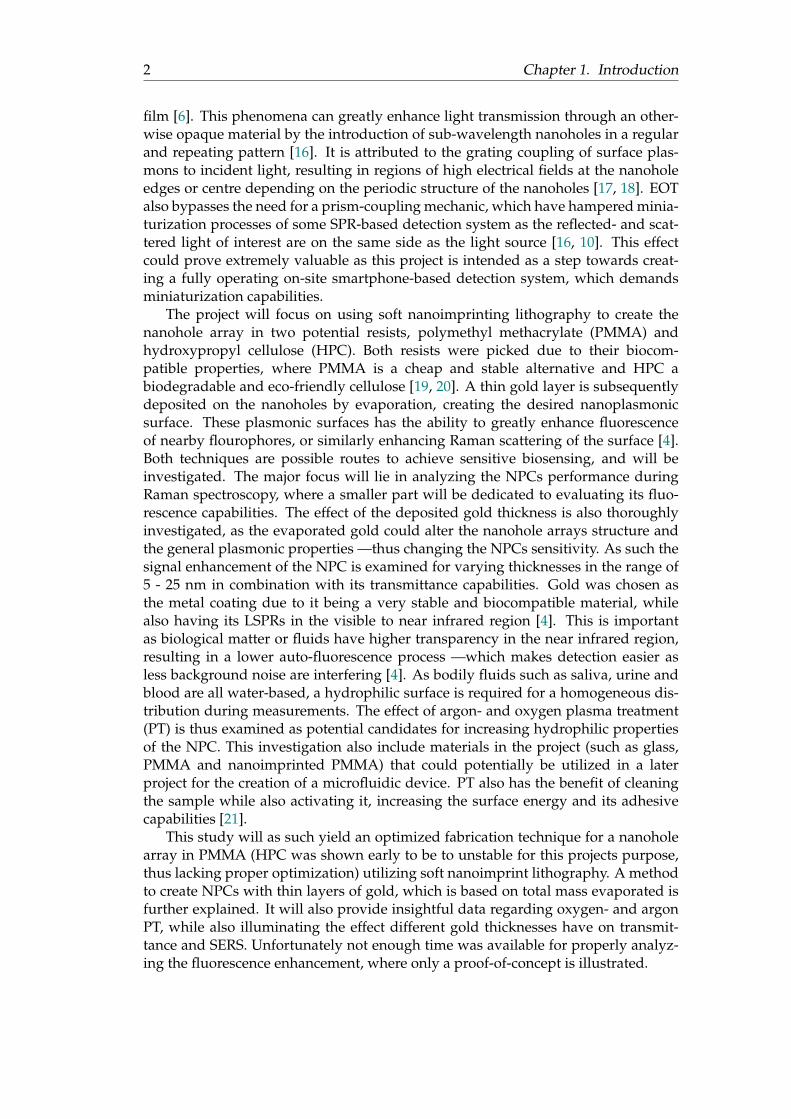
A plasmon is the quanta of plasma oscillation and together they form the collectiveoscillations of the free electrons in a metal [22]. At the surface of a metal these plas-mons take the form of surface plasmons. If the material have both a negative realand a small positive imaginary dielectric constant it has the ability to support SPR[23]. Incident electromagnetic (EM) radiation can couple to the surface plasmons andproduce standing or propagating surface modes of the electron density. As these ex-cited surface plasmons are created by the varying electric field of the incoming light,the light waves with wave vectors as parallel to the surface as possible will couplethe most efficiently [22]. The coupling of the SPR with incident light in combinationwith a sub-wavelength periodic nanohole structure is further attributed to be thecause of the EOT phenomenon [16].
A localized surface plasmon (LSP) occurs when a particle with smaller size thenthe incident lights wavelength is in the vicinity of a surface plasmon. Resulting inan oscillation of the free electrons of the nanoparticle in tune to the collective sur-face plasmon oscillation, see Fig. 2.1A [24]. These LSPs have the ability to greatlyenhance the electric field near the nanoparticle, with a tunable resonance frequencywhich strongly depend on the composition, size, particle-to-particle separation dis-tance, geometry and dielectric environment [22, 24]. Localized surface plasmon res-onance indicates when the LSPs have been excited by light at an optimal wavelengthand are oscillating at their resonance frequency.
2.2 Surface Enhanced Raman Spectroscopy
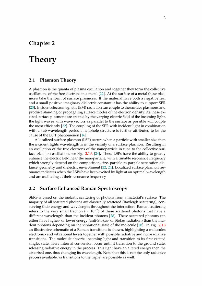
SERS is based on the inelastic scattering of photons from a material’s surface. Themajority of all scattered photons are elastically scattered (Rayleigh scattering), con-serving their energy and wavelength throughout the interaction. Raman scatteringrefers to the very small fraction (∼ 10−7) of these scattered photons that have adifferent wavelength than the incident photons [28]. These scattered photons caneither have higher- or lower energy (anti-Stokes- or Stokes radiation) than the inci-dent photons depending on the vibrational state of the molecule [28]. In Fig. 2.1Ban illustrative schematic of a Raman transitions is shown, highlighting a moleculeselectronic- and vibrational levels together with possible radiative and non-radiativetransitions. The molecule absorbs incoming light and transition to its first excitedsinglet state. Here internal conversion occur until it transition to the ground state,releasing radiative energy in the process. This light have an altered energy then theabsorbed one, thus changing its wavelength. Note that this is not the only radiativeprocess available, as transitions to the triplet are possible as well.
4 Chapter 2. Theory
As the Raman scattering is proportional to the magnitude of the change in po-larizability, aromatic molecules exhibit a stronger Raman scattering than aliphaticmolecules [29]. Molecules also have their own Raman spectrum —as different func-tional groups have their own unique characteristic vibrational energy— which canbe used for labeling and detection [29]. Unfortunately Raman scattering can provetroublesome to detect, as many samples may prove to be fluorescent by nature. Thecross-section (the likelihood of an interaction between two particles) of fluorescenceis on the order of 10−16 cm2 per molecule whereas the Raman cross section lies in therange of 10−31 to 10−26 cm2 per molecule [28]. If a laser with a wavelength that ex-cites these flourophores is used fluorescence will dominate over Raman scattering,as it is the more probable interaction to occur.
SERS is the enhancing of the Raman signal from a molecule by introducing ametal surface in its proximity. The enhancement is due to at least two effects, anEM- and chemical enhancement procedure. The EM enhancement is believed toattribute the most and works on the principle of molecules experiencing large localfield enhancements (hotspots) due to LSPR close to the metal [30]. For these fieldenhancements to have an effect on the molecule its distance from the metallic surface
(A)
(B)
(C)
FIGURE 2.1: A) Localized surface plasmon resonance occuring around metallic nanopar-ticles due to incident EM radiation. (Modified from Cytodiagnostics - Gold NanoparticleProperties, from Ref. [25]) B) Jablonski diagram of a molecules electronic- and vibrationalstates. A possible Raman transition is shown were a dotted line represent a radiative tran-sition and solid line a non-radiative transition. Do note that a possible transition from thesinglet to triplet state is possible, resulting in a radiative process. (Modified from Fig. 2.1 inRef. [26]) C) Jablonski diagram of excitation- and decay rates of a fluorophore in free spaceand in the proximity of metallic particles, colloids or surfaces. The decline in energy levelafter excitation is due to internal conversion, where some energy is transformed to heat.
(Modified from Fig. 3 in Ref. [27])
2.3. Metal Enhanced Fluorescence 5
should be within a few nanometers [31]. The chemical enhancement contribution isthought to be much less than the EM part and require the molecule to be chemicallyadsorbed on the surface, where a charge-transfer state can be created to enhance theRaman signal [29].
2.3 Metal Enhanced Fluorescence
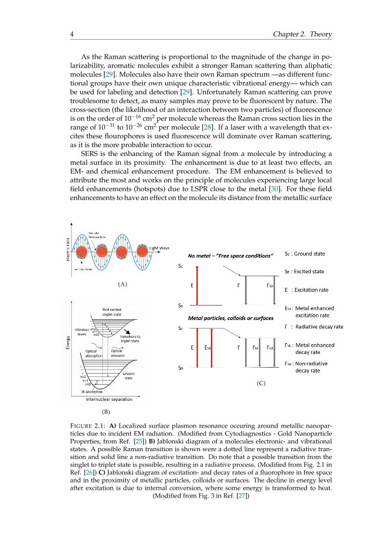
By introducing conductive metallic particles, surfaces or colloids in the vicinity of afluorophore (a chemical compound that can re-emit light upon excitation) it is pos-sible to alter the free-space conditions in ways that can result in remarkable spectralchanges [27]. This effect is called metal enhanced fluorescence (MEF) and is dueto at least three known mechanics experienced by the fluorophore. Namely energytransfer quenching to the metal, a changed incident electrical field and an alteredintrinsic radiative decay rate of the fluorophore [27]. The quenching occurs at rel-atively short distances (∼ 0-5 nm) from the metallic surface and can be thought ofas a damping of the fluorophores dipole oscillation due to the proximity of the freeelectrons in the metal, which result in a reduction of the total fluorescence [27, 32].The metallic nanoparticles will concentrate the electric field in their vicinity, whichcan increase the incident electric field experienced by the fluorophore and lead tohigher excitation rates [4, 32]. The change in radiative decay rate (∼ 0-20 nm) of thefluorophore is attributed to an increase in quantum yield (the amount of time fluo-rescence occurs per photon absorbed) due to the metals proximity and a correlatedreduction in lifetime —leading to higher fluorescence rates [32]. It can be illustrativeto consider the mathematical description of the quantum yield (Qm) and lifetime ofthe fluorophore (τm) in the vicinity of a metal to fully understand this:
Qm = (Γ + Γm)/(Γ + Γm + ΓNR) (2.1)
τm = 1/(Γ + Γm + ΓNR) (2.2)
where Γ is the radiative decay rate, Γm the enhanced decay rate due to the metaland ΓNR the total non-radiative decay rate. If Γm increase so will the quantum yieldin Eq. 2.1, while the lifetime seen in Eq. 2.2 decrease. In Fig. 2.1C an illustrativeJablonsky diagram of this process can be found, where a fluorophore is excited fromits ground state with and without metal present. Several other factors can affect thefluorescence intensity, as fluorophores are sensitive to environmental changes suchas pH, polarity, oxidation, temperature and distance to the metal [4].

7
Chapter 3
Method
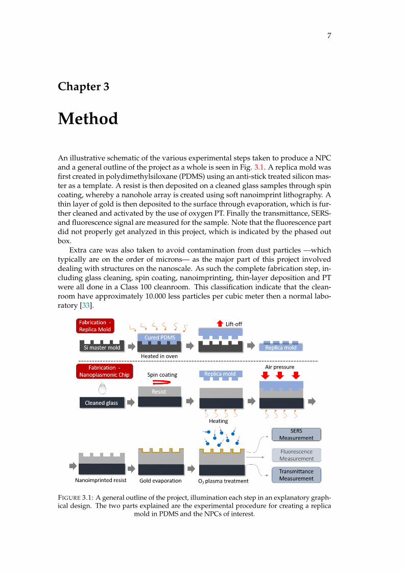
An illustrative schematic of the various experimental steps taken to produce a NPCand a general outline of the project as a whole is seen in Fig. 3.1. A replica mold wasfirst created in polydimethylsiloxane (PDMS) using an anti-stick treated silicon mas-ter as a template. A resist is then deposited on a cleaned glass samples through spincoating, whereby a nanohole array is created using soft nanoimprint lithography. Athin layer of gold is then deposited to the surface through evaporation, which is fur-ther cleaned and activated by the use of oxygen PT. Finally the transmittance, SERS-and fluorescence signal are measured for the sample. Note that the fluorescence partdid not properly get analyzed in this project, which is indicated by the phased outbox.
Extra care was also taken to avoid contamination from dust particles —whichtypically are on the order of microns— as the major part of this project involveddealing with structures on the nanoscale. As such the complete fabrication step, in-cluding glass cleaning, spin coating, nanoimprinting, thin-layer deposition and PTwere all done in a Class 100 cleanroom. This classification indicate that the clean-room have approximately 10.000 less particles per cubic meter then a normal labo-ratory [33].
FIGURE 3.1: A general outline of the project, illumination each step in an explanatory graph-ical design. The two parts explained are the experimental procedure for creating a replica
mold in PDMS and the NPCs of interest.

8 Chapter 3. Method
3.1 Equipment & Material
3.1.1 Material
All chemicals in the project were bought from Sigma Aldrich. These include ace-ton, ethanol, isopropanol, hexamethyyldisilazane, polydimethylsiloxane with cu-rant, rhoadmine 6G, anisole, de-ionized water, 100k (molecular weight) hydrox-ypropyl cellulose, 25k (molecular weight) polymethyl methacrylate and labeled goatanti-Rabbit antibodies.
The components used during evaporation were further bought from KurtJ.Lesker and include tungsten boats and 99,99% pure gold pellets. Prepatternedsilicon master molds with nanoholes (50 nm deep with a diameter of 250 nm) werepurchased from NIL Technology Denmark. Thin aluminum sheets for nanoimprint-ing were bought from Obducat Sweden. The microscope glass used were madeby RS France and the atomic force microscopy cantilever (spring constant k=0.5 N)bought from Mikromash Europe.
3.1.2 Equipment
Spin coater
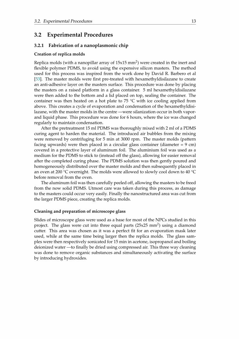
Spin coating is a simple but extremely useful method to fabricate a thin film on asample, as is illustrated in Fig. 3.2A. The material to be distributed is mixed withan appropriate solvent, creating a solution. The solution is then dispensed on asamples surface (usually via a pipette), which is held steady at a specific location bya vacuum pump. The sample is then rotated at high speed to distribute the solutionover the sample. The solvent is partially removed through evaporation during therotation and partly by a commonly used baking step at an appropriate temperature.The spin coater used was a SPS Spin 150 model from SPS Europe, see Fig. 3.3A.
Nanoimprint lithography
An EITRE® 3 Nano Imprint Lithography System from Obducat was used for allimprints in this project, see Fig. 3.3B. This system allows for imprinting using onlythe soft pressure from compressed air, ensuring pressure uniformity over the wholeimprint area. To maintain this pressure during the imprint procedure, it is necessaryto cover the top part of a sample holder by a malleable but strong material. Thematerial needs to withstand deformation without breaking during the set imprintpressure to avoid leakage. A common material to use that fulfills these criteria arethin sheets of aluminum.
The EITRE® 3 system allows the user to create their own imprint programs, vary-ing parameters such as pressure, temperature, time and cooling. The cooling systemis based on air flow, where the sample holder is cooled from below to avoid affect-ing the imprint procedure. As is illustrated in Fig. 3.2C the basic principle behindthe nanoimprint system is temperature and pressure. A mold is placed on top of achosen resist and heat gradually applied from the bottom until the glass transitiontemperature of the resist is reached. At and beyond this temperature the resist ex-hibits malleable properties, allowing for imprints to be done with a correctly appliedpressure.
3.1. Equipment & Material 9
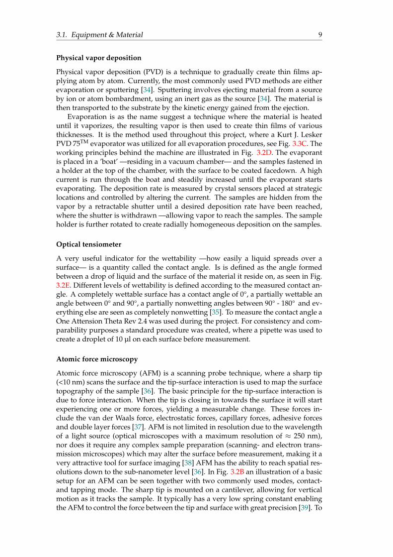
Physical vapor deposition
Physical vapor deposition (PVD) is a technique to gradually create thin films ap-plying atom by atom. Currently, the most commonly used PVD methods are eitherevaporation or sputtering [34]. Sputtering involves ejecting material from a sourceby ion or atom bombardment, using an inert gas as the source [34]. The material isthen transported to the substrate by the kinetic energy gained from the ejection.
Evaporation is as the name suggest a technique where the material is heateduntil it vaporizes, the resulting vapor is then used to create thin films of variousthicknesses. It is the method used throughout this project, where a Kurt J. LeskerPVD 75TM evaporator was utilized for all evaporation procedures, see Fig. 3.3C. Theworking principles behind the machine are illustrated in Fig. 3.2D. The evaporantis placed in a ’boat’ —residing in a vacuum chamber— and the samples fastened ina holder at the top of the chamber, with the surface to be coated facedown. A highcurrent is run through the boat and steadily increased until the evaporant startsevaporating. The deposition rate is measured by crystal sensors placed at strategiclocations and controlled by altering the current. The samples are hidden from thevapor by a retractable shutter until a desired deposition rate have been reached,where the shutter is withdrawn —allowing vapor to reach the samples. The sampleholder is further rotated to create radially homogeneous deposition on the samples.
Optical tensiometer
A very useful indicator for the wettability —how easily a liquid spreads over asurface— is a quantity called the contact angle. Is is defined as the angle formedbetween a drop of liquid and the surface of the material it reside on, as seen in Fig.3.2E. Different levels of wettability is defined according to the measured contact an-gle. A completely wettable surface has a contact angle of 0°, a partially wettable anangle between 0° and 90°, a partially nonwetting angles between 90° - 180° and ev-erything else are seen as completely nonwetting [35]. To measure the contact angle aOne Attension Theta Rev 2.4 was used during the project. For consistency and com-parability purposes a standard procedure was created, where a pipette was used tocreate a droplet of 10 µl on each surface before measurement.
Atomic force microscopy
Atomic force microscopy (AFM) is a scanning probe technique, where a sharp tip(<10 nm) scans the surface and the tip-surface interaction is used to map the surfacetopography of the sample [36]. The basic principle for the tip-surface interaction isdue to force interaction. When the tip is closing in towards the surface it will startexperiencing one or more forces, yielding a measurable change. These forces in-clude the van der Waals force, electrostatic forces, capillary forces, adhesive forcesand double layer forces [37]. AFM is not limited in resolution due to the wavelengthof a light source (optical microscopes with a maximum resolution of ≈ 250 nm),nor does it require any complex sample preparation (scanning- and electron trans-mission microscopes) which may alter the surface before measurement, making it avery attractive tool for surface imaging [38] AFM has the ability to reach spatial res-olutions down to the sub-nanometer level [36]. In Fig. 3.2B an illustration of a basicsetup for an AFM can be seen together with two commonly used modes, contact-and tapping mode. The sharp tip is mounted on a cantilever, allowing for verticalmotion as it tracks the sample. It typically has a very low spring constant enablingthe AFM to control the force between the tip and surface with great precision [39]. To
10 Chapter 3. Method
allow three dimensional movement the cantilever or sample is mounted on a piezo-electric scanner, which allow for high accuracy of sample positioning. The actualmeasurement is done by focusing a laser beam on the tip of the cantilever, whichis reflected to a 4-quadrant photo-sensitive detector (PSD) for 2D mapping. As thetip scans a surface the force it experiences will alter the cantilevers position and theangle of reflection of the laser will change, moving the laser spot on the PSD. Thisleads to a measurable change in intensity on each quadrant, which can be used forimaging. The AFM used in this project is a MultimodeTM Atomic Force Microscopeat room temperature. see Fig. 3.3E. This AFM has two available modes for scanninga surface, contact- and tapping mode. During contact mode the tip is brought intoclose contact of the sample and kept there during the scan, which usually damagethe surface. Using tapping mode yields less risk of damaging the surface, as lesscontact to the surface is done. In this mode the cantilever is excited by an electricaloscillator creating a vertically oscillatory motion, effectively tapping the surface inshort intervals —reducing the lateral force experienced by the surface. This modewas used in all AFM scans during the project.
(A) (B)
(C) (D) (E)
FIGURE 3.2: A) A spin coating process shown in an illustrative way. (Modified from Fig. 2in Ref. [40].) B) Basic principles of an AFM with two possible operation modes. (Modifedfrom Fig. 1 in Ref. [38].) C) Illustration of the nanoimprint litography process. Note that theair pressure is applied from all directions for a homogeneous imprint. (Modifed from Fig.1A in Ref. [19]) D) The PVD setup used for evaporation, with explanatory text of the moreimportant components. (Modifed from Fig. 2.3B in Ref. [41]) E) Illustration of a 10 µl drop
pippeted on a surface during a contact angle measurement.
3.1. Equipment & Material 11
Plasma treatment system
Surface treatment is the act of cleaning a surface by removing loose materials ormodifying the surface through chemical- or physical operations [42]. As such plentyof methods are defined as surface treatment procedures, but throughout this projectthe focus lie on utilizing plasma to clean and activate the NPCs surface.
A plasma (referred to as the fourth state of matter) is a collective of chargedparticles containing positive ions, negative ions and other fragments —such as freeradicals, atoms and molecules. It is produced by exciting a gas with electrical energyand is highly reactive [43]. Depending on the source gas different effects will domi-nate during PT. Argon physically bombarded a surface with ions and atoms, whereoxygen remove contaminants through chemical reactions [44]. An ATTO PlasmaSurface Treatment Machine from Diener Electronics (with a maximum power of 50W) was used in this project, see Fig. 3.3D. The machine had access to both argon andoxygen, utilizing cold and low pressure (vacuum plasma) PT.
Scanning electron microscopy
A scanning electron microscope (SEM) works on the principle of accelerating highenergy electrons (0.1 - 30 keV) towards a samples surface [45]. The electron beaminteract with the surface producing secondary electrons, backscattered electrons,Auger electrons, x-rays and possibly light —which are all collected for imaging bymultiple sensors designed for specific areas, such as a backscatter electron detector[46]. In comparison to the maximum useful magnification of an optical microscopes(around 1000x) using SEM allows magnifications of 300.000x to be reached [45, 46].One negative aspect to be considered when using SEM is that non-conductive sam-ples will experience surface charging due to the electron beam, distorting the surfaceimage [47]. To avoid this the sample need either be conductive by nature or have aconductive medium applied to the surface. Throughout this project a Carl ZeissMerlin Field Emission SEM model was used.
Fluorescence system
The fluorescence measurements were done using a LI-COR Odyssey SA. The ma-chine has two channels, allowing for illumination by an infrared laser at wave-lengths λ1 = 700 nm or λ2 = 800 nm. The resulting fluorescence is then measuredsystematically as the laser beam scans the full area of the sample. The image cre-ated is thus a surface with different pixels of varying fluorescence intensities. Thesepixels can then be analyzed to find the fluorescence intensity at different regions.
Raman spectroscopy
The surface enhanced Raman measurements were done using a Renishaw® InviaRaman Microscope StreamlineTM. A laser with wavelength λ = 785 nm with maxi-mum power of 500 mW were used together with a grating consisting of 1200 l/mm.The grating is used to split the refracted light into its constitutional wavelengths,before measuring their respective intensity.
12 Chapter 3. Method
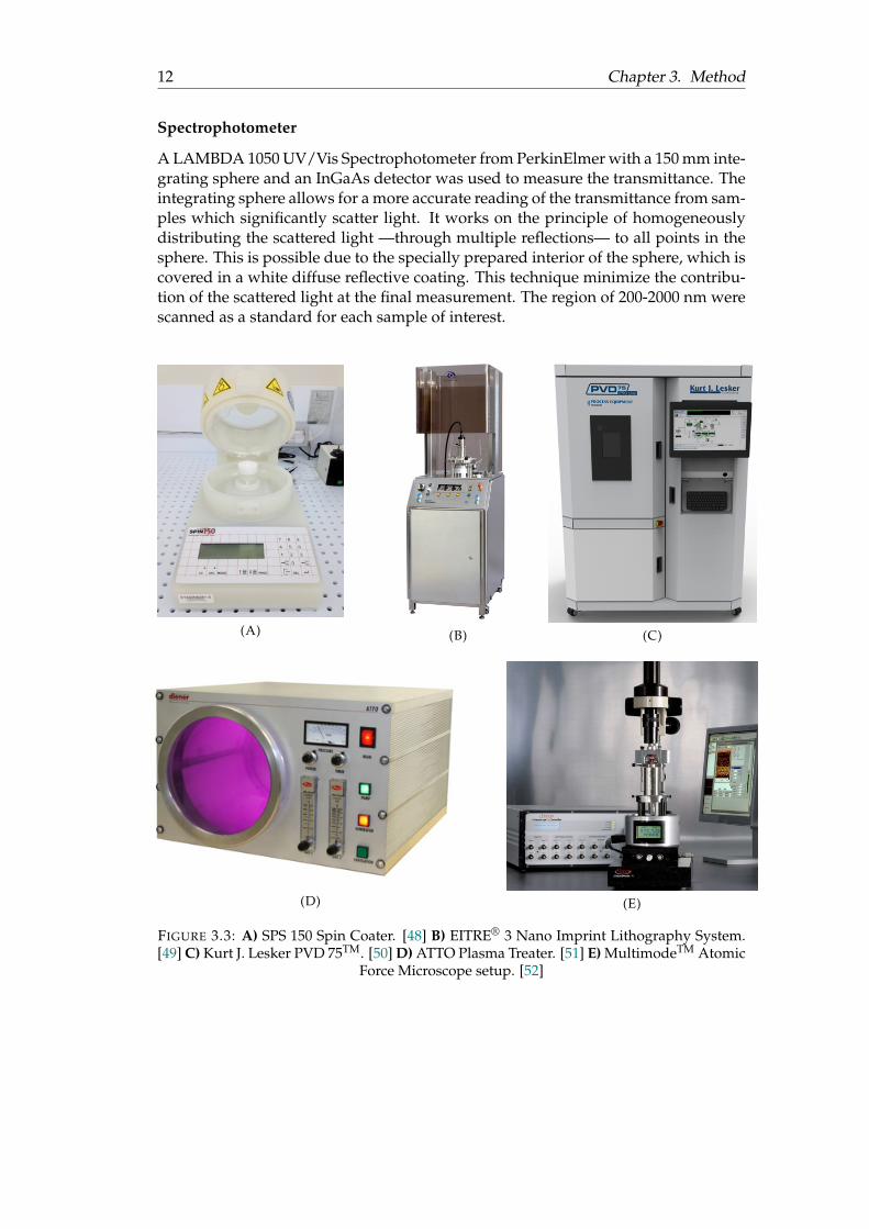
Spectrophotometer
A LAMBDA 1050 UV/Vis Spectrophotometer from PerkinElmer with a 150 mm inte-grating sphere and an InGaAs detector was used to measure the transmittance. Theintegrating sphere allows for a more accurate reading of the transmittance from sam-ples which significantly scatter light. It works on the principle of homogeneouslydistributing the scattered light —through multiple reflections— to all points in thesphere. This is possible due to the specially prepared interior of the sphere, which iscovered in a white diffuse reflective coating. This technique minimize the contribu-tion of the scattered light at the final measurement. The region of 200-2000 nm werescanned as a standard for each sample of interest.
(A) (B) (C)
(D) (E)
FIGURE 3.3: A) SPS 150 Spin Coater. [48] B) EITRE® 3 Nano Imprint Lithography System.[49] C) Kurt J. Lesker PVD 75TM. [50] D) ATTO Plasma Treater. [51] E) MultimodeTM Atomic
Force Microscope setup. [52]
3.2. Experimental Procedures 13
3.2 Experimental Procedures
3.2.1 Fabrication of a nanoplasmonic chip
Creation of replica molds
Replica molds (with a nanopillar array of 15x15 mm2) were created in the inert andflexible polymer PDMS, to avoid using the expensive silicon masters. The methodused for this process was inspired from the work done by David R. Barbero et al[53]. The master molds were first pre-treated with hexamethyldisilazane to createan anti-adhesive layer on the masters surface. This procedure was done by placingthe masters on a raised platform in a glass container. 5 ml hexamethyldisilazanewere then added to the bottom and a lid placed on top, sealing the container. Thecontainer was then heated on a hot plate to 75 °C with ice cooling applied fromabove. This creates a cycle of evaporation and condensation of the hexamethyldisi-lazane, with the master molds in the centre —were silanization occur in both vapor-and liquid phase. This procedure was done for 6 hours, where the ice was changedregularly to maintain condensation.
After the pretreatment 15 ml PDMS was thoroughly mixed with 2 ml of a PDMScuring agent to harden the material. The introduced air bubbles from the mixingwere removed by centrifuging for 5 min at 3000 rpm. The master molds (patternfacing upwards) were then placed in a circular glass container (diameter = 9 cm)covered in a protective layer of aluminum foil. The aluminium foil was used as amedium for the PDMS to stick to (instead off the glass), allowing for easier removalafter the completed curing phase. The PDMS solution was then gently poured andhomogeneously distributed over the master molds and then subsequently placed inan oven at 200 °C overnight. The molds were allowed to slowly cool down to 40 °Cbefore removal from the oven.
The aluminum foil was then carefully peeled off, allowing the masters to be freedfrom the now solid PDMS. Utmost care was taken during this process, as damageto the masters could occur very easily. Finally the nanostructured area was cut fromthe larger PDMS piece, creating the replica molds.
Cleaning and preparation of microscope glass
Slides of microscope glass were used as a base for most of the NPCs studied in thisproject. The glass were cut into three equal parts (25x25 mm2) using a diamondcutter. This area was chosen as it was a perfect fit for an evaporation mask laterused, while at the same time being larger then the replica molds. The glass sam-ples were then respectively sonicated for 15 min in acetone, isopropanol and boilingdeionized water —to finally be dried using compressed air. This three way cleaningwas done to remove organic substances and simultaneously activating the surfaceby introducing hydroxides.
14 Chapter 3. Method
Resist preparation and thin layer deposition by spin coating
A PMMA solution was prepared by mixing a 25 K molecular weight powder withanisole. The solution were sonicated for 30 minutes and left overnight, where it wascompletely dissolved the following morning. For consistency and reproducibilitypurposes a 5 weight % PMMA solution were set as standard and used through-out the whole project. Simlarly a 5 weight % solution of HPCA were prepared bymixing a 100 k molecular weight powder with water. The solution was sonicatedfor 30 minutes and left overnight. The spin coating process were equally done forboth solutions where 150 µl was pipetted on a cleaned glass substrate and gentlydistributed over the whole sample. This was done as the PMMA solution exhib-ited tendencies for inhomogeneous distribution after spin coating. if only using thedrop-on method. No spin curve data (deposited thickness versus rpm) were foundfor the molecular weights of HPC and PMMA used. By extrapolating data fromother molecular weights an educated guess could be made that 2000 rpm wouldcreate a thick enough layer to sustain the expected 50 nm deep nanoholes. Thisthickness was verified using AFM and found to be close to 100 nm for PMMA. Afterspin coating at 2000 rpm for 60 seconds the samples were baked for at least 10 min-utes on a hot bed at 100 °C, removing residue solvents and moisture. This procedurewas set as standard for all samples.
Nanoimprinting lithography optimization
To find the optimal nanoimprinting parameters a thorough investigation of temper-ature, pressure and time was done by fixing two parameters and varying the third.Each sample were allowed to cool to 45 °C before removal —to avoid disturbing thenanoimprint procedure, and possibly altering the final imprint. The surface of eachsample was investigated by AFM to determine the effect the parameter had on theshape of the imprinted nanoholes. The sharp edges of the microscope glass provedslightly problematic as it tended to break the protecting aluminum sheets duringthe imprint, leading to pressure loss. To avoid this problem two imprint masks werecreated (a single imprint and double imprint version) from a polymer tested to with-stand 200 °C for 4 hours. To avoid adhesion problems between the mask and sampleholder microscope glass were cut in suitable dimensions and fastened to the bottomof the mask before each imprint. Two aluminum sheets still had to be used to main-tain the pressure, as even the the more soft polymer edges of the masks were enoughto cause pressure loss when using a single layer.
As the glass transition temperature of PMMA varies depending on its molecu-lar weight, temperature was the first parameter to be investigated [54]. A range of110 °C - 150 °C were examined while fixing pressure and imprint time to 20 bar and15 min. Pressure and time were then varied for interesting temperatures. The finalnanoimprints for the NPCs were done with a pressure of 5 bar, temperature of 115°C and an imprint period of 5 minutes. A similar process was done for HPC, wherean imprint recipe was inspired by the work of Camilla Dore et al [19]. Nanoim-prints on HPC were done using a temperature of 140 °C, 20 bar pressure and 15min imprint time. The contact angle was further measured for multiple samples—including PMMA and nanoimprinted PMMA of varying forms— during this op-timization procedure. Three measurements were done and the average taken asthe samples contact angle, this was set as standard for any subsequent measure-ments. Furthermore regular spots checks of a nanoimprinted surface where doneusing AFM, to see how the mold deteriorated by use.
3.2. Experimental Procedures 15
Thin layer deposition - evaporation of gold
Usually this process is rather straight forward, an evaporant is placed in a suitableboat and heated until vaporization. The crystal sensors then regulate the deposi-tion rate by controlling the applied power to achieve the desired final thickness.Due to malfunctions of the evaporator this was proved problematic, as the deposi-tion rate did not register properly. This problem started occurring halfway into theproject and persisted after sensor replacement. As such some metal coatings weremuch thicker than intended. To circumvent this problem the shutters were set tobe completely open from the start and the thickness controlled by the amount ofmass evaporated. As such an investigating of mass versus thickness was done byevaporating different milligrams of gold on cleaned glass. The samples thicknesswere measured by AFM by making multiple cuts through the gold using a plasticutensil. Three cut regions were then scanned and the average recorded. The surfacemorphology of cleaned glass was further investigated and found to only vary onthe sub-nanometer level, allowing for accurate thickness measurements. Further-more a 3x3 mask (holding a total of nine samples) was used to fix the samples in aspecific location during each evaporation procedure, thus avoiding possible radialvariations. A tungsten boat was used to contain and heat the gold during all evap-oration procedures. The boat was fastened in such a way that its position could bereproduced during a later evaporation. Using this method five NPCs with differ-ent thicknesses were created using the mass seen in Table 3.1. AFM and SEM wasused to characterize the surface morphology of the different NPCs. Furthermore thecontact angle was measured for each sample.
TABLE 3.1: The corresponding thickness to evaporated mass of goldof the five investigated samples. The standard error of the mean isshown for the thickness, where it was approximated from the sample
standard deviation.
Mass of gold [mg] Deposited Thickness [nm]
32 5 ±161 5 ±1
123 13 ±2176 18 ±2246 21 ±1
3.2.2 Plasma treatment optimization
Multiple tests were done using either argon or oxygen to plasma treat interest-ing surfaces or materials. This include cleaned glass, spin coated PMMA, nanoim-printed PMMA and the NPC at various thicknesses. The general procedure takenwas to fix the power at 50 W and vary the exposure time. The wettability differenceof each surface was checked by measuring the contact angle before and after treat-ment. Each surface was further investigated using AFM after each treatment, as noguarantee of the PT being unharmful to any surface existed.
16 Chapter 3. Method
3.2.3 Surface enhanced Raman spectrosopy measurements
Each SERS spectra was obtained by measuring the molecule rhoadmine 6G (R6G) onthe NPCs. R6G is an extremely potent fluorophore when excited by visible radiation.However when adsorbed to a metal surface this process gets quenched and a verystrong Raman signal can be observed [55]. A solution of 10 mM R6G in ethanol wereprepared and further diluted to prepare 100 µM, 10 µM, 1 µM, 100 nM and 10 nM.To find the sample with the best enhancement 100 µM was used as a standard. 20µL was applied to the surface and the sample left to air dry. The signal-to-noise ratioof the NPCs were then measured and compared versus control samples from thesame evaporation process. The best sample was then further investigated with theremaining molarities to find the NPCs detection limit.
3.2.4 Fluorescence measurements
Unfortunately not enough time was available to do a proper fluorescence evalua-tion of the NPCs. The technique was however tested using labeled goat Anti-Rabbitantibodies. A solution was prepared using the ratio 1mg/1ml of antibodies and dis-tilled water. The solution was then diluted into different concentrations with ratiosbetween 1:1K - 1:100K. These were then dropped on the sample and the fluorescencemeasured.
3.2.5 Transmittance measurements
No special procedure had to be done for measuring the transmittance. The samplewas placed in a sample holder for chip-like structures outside the integrating sphere.The transmittance was then measured using a detector in the integrating sphere forwavelengths in the range of 200-2000 nm. This procedure was done for all NPCswith some control samples of glass with gold layers of similar thickness.
17
Chapter 4
Results & Discussion
In this chapter the major results of the project will be presented and discussed ina relevant manner. The results will be shown similarly to how the work procedurewas done, that is from the creation of the replica mold to the final transmittance- andSERS measurements.
4.1 Nanoimprints & Replica mold
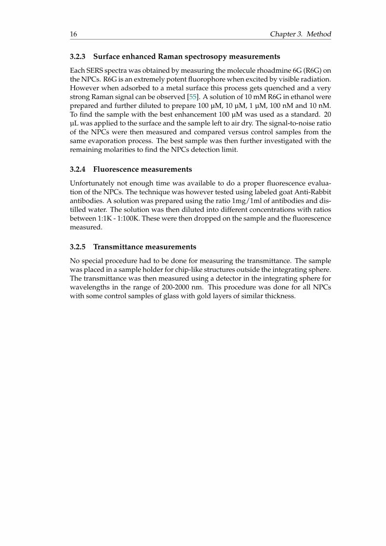
In order to achieve adequate nanoimprints using soft nanoimprint lithography, tem-perature was shown to be a major factor to be taken into consideration. In Fig. 4.1B,4.1C and 4.1D the temperature dependence of imprints on PMMA is illustrated atthree different temperatures, while keeping pressure and time fixed. As the temper-ature gets gradually lower the nanoholes get more and more distinct. The surface ofthe replica mold was further characterized with AFM, to exclude the possibility of adefect in the replica molds nanopillars. The surface profile is illustrated in Fig 4.1Aand a nanopillar profile in Fig. 4.2D. From these pictures we observe a homogenouspattern of circular pillars from a topview, with heights of 47-48 nm. As such thiseffect is most likely due to the glass transition temperature of PMMA. The lower thetemperature used the less malleable the resist is, decreasing the possibility of moldmovements during the imprint procedure —thus enabling better imprints. Pressureand time did not prove to be as significant as temperature, as adequate imprintswere done at 120 °C using both low and high pressures (5 - 30 bar) in combina-tion with short and long imprint times (30 s - 15 min). The replica molds were alsochecked regularly to see if they deteriorated by use. After 16 imprints no change in
(A) (B) (C) (D)
FIGURE 4.1: Surface profiles of a replica mold and nanoimprints done on PMMA at varyingtemperatures. The pressure and imprint time were fixed at 20 bars and 15 min during allimprints. A) Replica mold in PDMS. B) Imprint done at 150 °C. C) Imprint done at 130 °C.
D) Imprint done at 120 °C.
18 Chapter 4. Results & Discussion
structure of the nanoimprints were observed, indicating a rather long survivabilityof the molds.
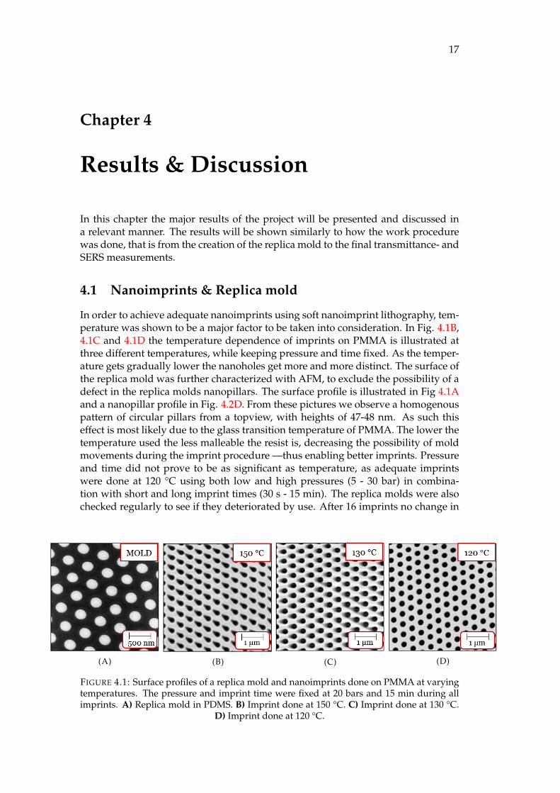
Some variations of the nanoimprint structure were however observed when us-ing 120 °C as imprint temperature. The tail observed at higher temperature, such asin Fig. 4.1B and 4.1C was found during both AFM and SEM surface scans, such asin Fig. 4.3A. This effect could either be due to 120 °C being to high a temperaturefor stable imprints, or a pressure related issue. During some imprints very smallpressure leakage occurred, where the software deemed the pressure in need of reg-ulation. This regulation was done by increasing the air pressure rapidly, creatingsmall pressure bumps that could have affected the imprint procedure. To avoid thisthe standard parameters for imprinting were set to to 115 °C, while using a pres-sure of 5 bar —which was an effective pressure limitation of the equipment used.It is possible that the nanoimprints could be achieved on PMMA using only atmo-spheric pressure. The temperature in close range of 120 °C also proved to drasticallyaffect the depths of the nanoholes. By lowering the temperature from 120 to 110 °Cthe depths of the holes changed by ≈ 30 nm as is seen in Fig. 4.2A, 4.2B and 4.2C. Assuch by moving from 120 °C —which was standard for imprints in the early stagesof the project— to 115 °C a depth of approximately 10 nm was lost. This was deemedacceptable for the possibility of creating more stable nanoholes with a sharp edge,hopefully leading to greater SERS- and fluorescence enhancement.
(A) (B)
(C) (D)
FIGURE 4.2: Height profiles of three nanoholes done with varying temperatures on PMMAand a nanopillar of the replica mold. A) 120 °C on PMMA. B) 115 °C. C) 110 °C. D) Replica
mold.
4.2. Physical Vapor Deposition & Nanoplasmonic Chip 19
(A) (B)
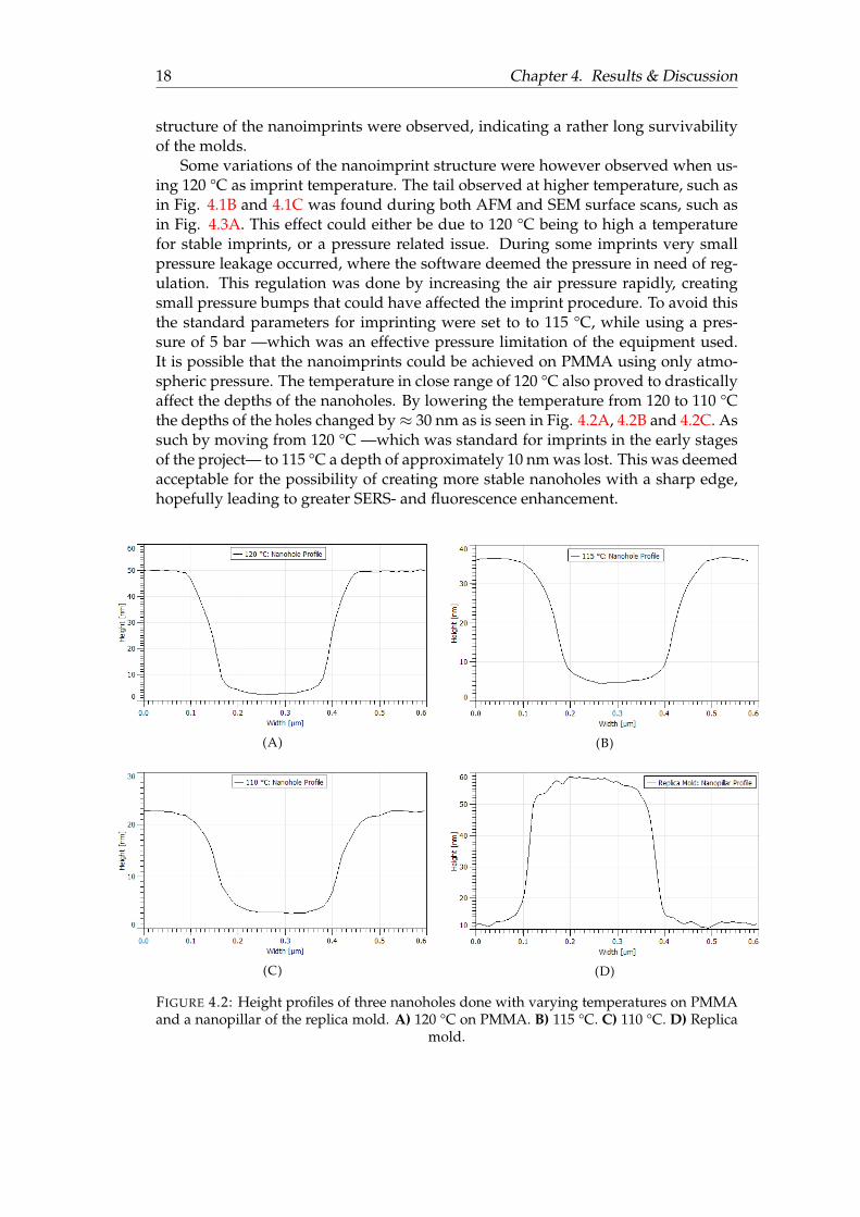
FIGURE 4.3: SEM pictures of nanohole structures covered in a thin layer of 20-30 nm (basedon transparency and color) gold at 100.000x magnification. A) PMMA imprint at 120 °C.Note that the edges of the nanoholes are less sharp in some locations, indicating a slope to
the bottom. B) HPC imprint at 150 °C.
A short investigation was also done to see if commercially accessible and cheapaluminum foil could prove a substitute to the more costly aluminum sheets usedduring the imprint procedure. Some success were achieved when stacking multiplelayers of four and above. Unfortunately it proved a very unstable method wherethe majority of the imprints still resulted in pressure loss. Reusing the aluminumsheets also proved problematic, since they easily got deformed during removal fromthe nanoimprinter. These deformations were enough to influence the imprints, ifouccuring at sensitive location. Industrial bought aluminum sheets with similar di-mensions to the pre-bought ones could however prove to be a possible and cheaperalternative to the one currently used.
Even though HPC was dropped quite early as a resist for the plasmonic chip—as water-based fluids were proven to easily damage the NPCs surface — it couldstill prove useful as a template. Good nanoimprints were achieved in the resist us-ing non-optimized parameters, as can be seen in Fig. 4.3B. These nanoimprints incombination with HPCs very potent ability to form a solution with water could beused in a method to fabricate nanopillars. By filling the nanoholes with a non water-soluble material (e.g. PMMA) and decomposing the original HPC template in water,one should theoretically be left with nanopillars in PMMA.
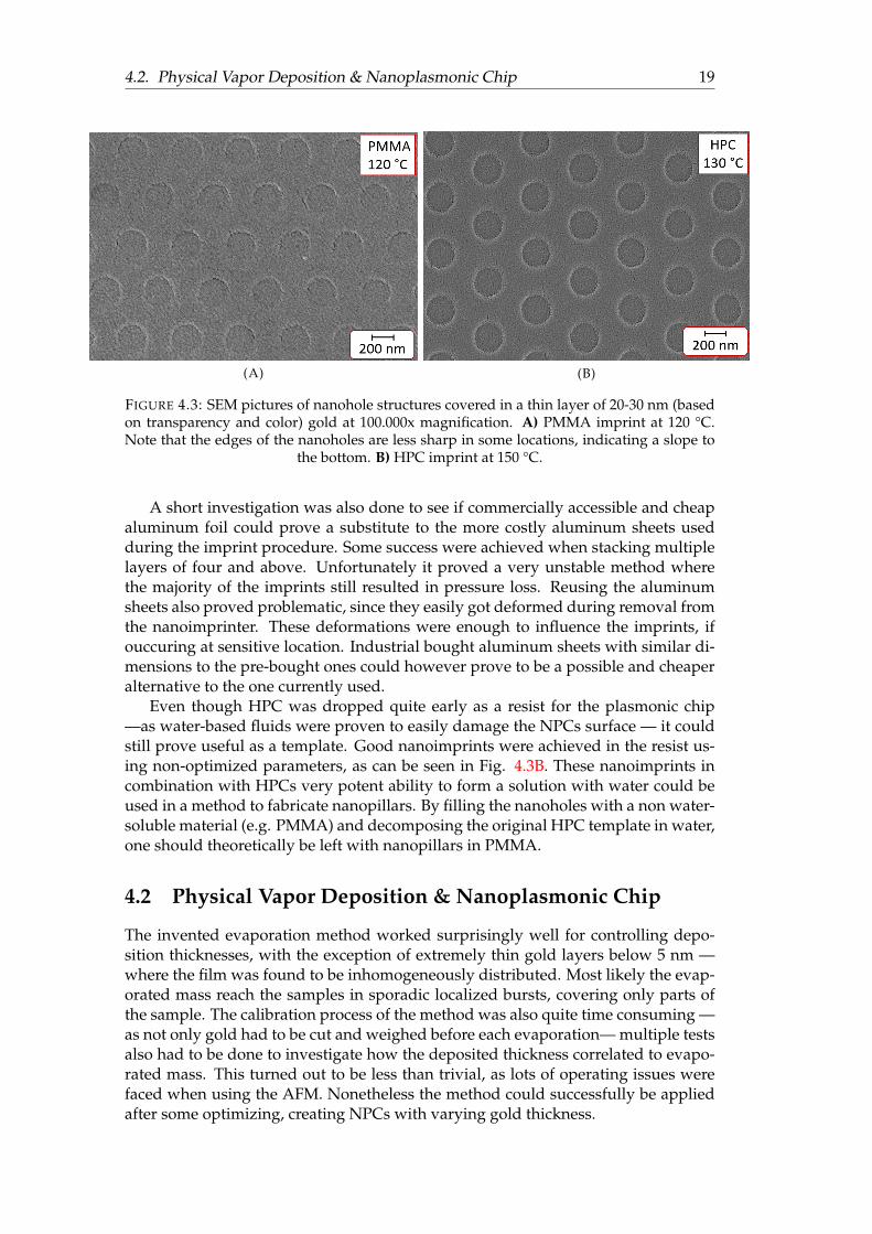
4.2 Physical Vapor Deposition & Nanoplasmonic Chip
The invented evaporation method worked surprisingly well for controlling depo-sition thicknesses, with the exception of extremely thin gold layers below 5 nm —where the film was found to be inhomogeneously distributed. Most likely the evap-orated mass reach the samples in sporadic localized bursts, covering only parts ofthe sample. The calibration process of the method was also quite time consuming —as not only gold had to be cut and weighed before each evaporation— multiple testsalso had to be done to investigate how the deposited thickness correlated to evapo-rated mass. This turned out to be less than trivial, as lots of operating issues werefaced when using the AFM. Nonetheless the method could successfully be appliedafter some optimizing, creating NPCs with varying gold thickness.
20 Chapter 4. Results & Discussion
(A)
(B)
(C)
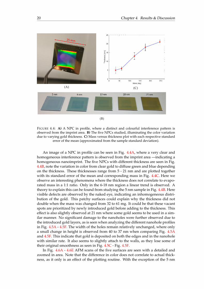
FIGURE 4.4: A) A NPC in profile, where a distinct and colourful interference pattern isobserved from the imprint area. B) The five NPCs studied, illuminating the color variationdue to varying gold thickness. C) Mass versus thickness plot with each respective standard
error of the mean (approximated from the sample standard deviation).
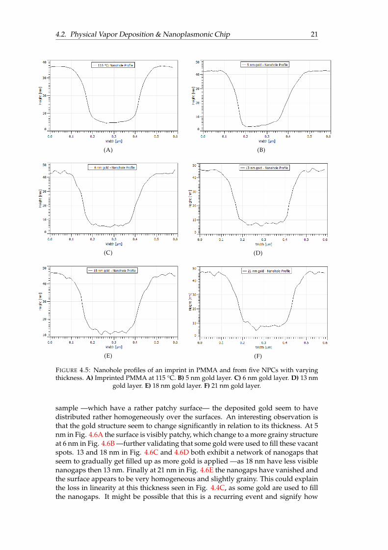
An image of a NPC in profile can be seen in Fig. 4.4A, where a very clear andhomogeneous interference pattern is observed from the imprint area —indicating ahomogeneous nanoimprint. The five NPCs with different thickness are seen in Fig.4.4B, note the variation in color from clear gold to diffuse green and blue dependingon the thickness. These thicknesses range from 5 - 21 nm and are plotted togetherwith its standard error of the mean and corresponding mass in Fig. 4.4C. Here weobserve an interesting phenomena where the thickness does not correlate to evapo-rated mass in a 1:1 ratio. Only in the 6-18 nm region a linear trend is observed. Atheory to explain this can be found from studying the 5 nm sample in Fig. 4.4B. Herevisible defects are observed by the naked eye, indicating an inhomogeneous distri-bution of the gold. This patchy surfaces could explain why the thickness did notdouble when the mass was changed from 32 to 61 mg. It could be that these vacantspots are prioritized by newly introduced gold before adding to the thickness. Thiseffect is also slightly observed at 21 nm where some gold seems to be used in a sim-ilar manner. No significant damage to the nanoholes were further observed due tothe introduced gold layers, as is seen when analyzing the different nanohole profilesin Fig. 4.5A - 4.5F. The width of the holes remain relatively unchanged, where onlya small change in height is observed from 40 to 37 nm when comparing Fig. 4.5Aand 4.5F. This indicate that gold is deposited on both the edges and in the nanoholewith similar rate. It also seems to slightly attach to the walls, as they lose some oftheir original smoothness as seen in Fig. 4.5C - Fig. 4.5F.
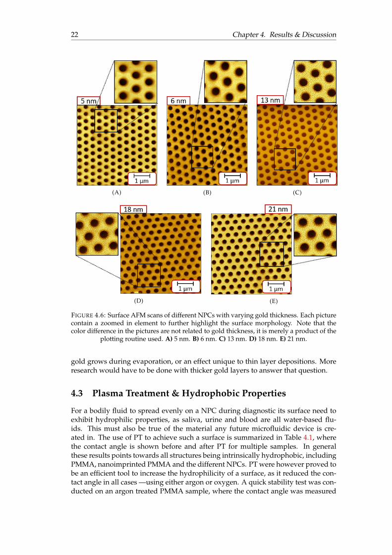
In Fig. 4.6A - 4.6E AFM scans of the five surfaces are seen with a detailed andzoomed in area. Note that the difference in color does not correlate to actual thick-ness, as it only is an effect of the plotting routine. With the exception of the 5 nm
4.2. Physical Vapor Deposition & Nanoplasmonic Chip 21
(A) (B)
(C) (D)
(E) (F)
FIGURE 4.5: Nanohole profiles of an imprint in PMMA and from five NPCs with varyingthickness. A) Imprinted PMMA at 115 °C. B) 5 nm gold layer. C) 6 nm gold layer. D) 13 nm
gold layer. E) 18 nm gold layer. F) 21 nm gold layer.
sample —which have a rather patchy surface— the deposited gold seem to havedistributed rather homogeneously over the surfaces. An interesting observation isthat the gold structure seem to change significantly in relation to its thickness. At 5nm in Fig. 4.6A the surface is visibly patchy, which change to a more grainy structureat 6 nm in Fig. 4.6B —further validating that some gold were used to fill these vacantspots. 13 and 18 nm in Fig. 4.6C and 4.6D both exhibit a network of nanogaps thatseem to gradually get filled up as more gold is applied —as 18 nm have less visiblenanogaps then 13 nm. Finally at 21 nm in Fig. 4.6E the nanogaps have vanished andthe surface appears to be very homogeneous and slightly grainy. This could explainthe loss in linearity at this thickness seen in Fig. 4.4C, as some gold are used to fillthe nanogaps. It might be possible that this is a recurring event and signify how
22 Chapter 4. Results & Discussion
(A) (B) (C)
(D) (E)
FIGURE 4.6: Surface AFM scans of different NPCs with varying gold thickness. Each picturecontain a zoomed in element to further highlight the surface morphology. Note that thecolor difference in the pictures are not related to gold thickness, it is merely a product of the
plotting routine used. A) 5 nm. B) 6 nm. C) 13 nm. D) 18 nm. E) 21 nm.
gold grows during evaporation, or an effect unique to thin layer depositions. Moreresearch would have to be done with thicker gold layers to answer that question.
4.3 Plasma Treatment & Hydrophobic Properties
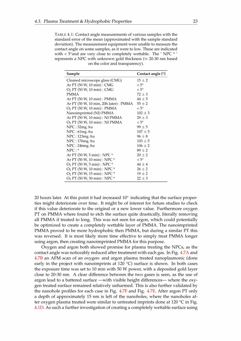
For a bodily fluid to spread evenly on a NPC during diagnostic its surface need toexhibit hydrophilic properties, as saliva, urine and blood are all water-based flu-ids. This must also be true of the material any future microfluidic device is cre-ated in. The use of PT to achieve such a surface is summarized in Table 4.1, wherethe contact angle is shown before and after PT for multiple samples. In generalthese results points towards all structures being intrinsically hydrophobic, includingPMMA, nanoimprinted PMMA and the different NPCs. PT were however proved tobe an efficient tool to increase the hydrophilicity of a surface, as it reduced the con-tact angle in all cases —using either argon or oxygen. A quick stability test was con-ducted on an argon treated PMMA sample, where the contact angle was measured
4.3. Plasma Treatment & Hydrophobic Properties 23
TABLE 4.1: Contact angle measurements of various samples with thestandard error of the mean (approximated with the sample standarddeviation). The measurement equipment were unable to measure thecontact angle on some samples, as it were to low. These are indicatedwith < 5°and are very close to completely wettable. The ’ NPC * ’represents a NPC with unknown gold thickness (≈ 20-30 nm based
on the color and transparency).
Sample Contact angle [°]
Cleaned microscope glass (CMG) 15 ± 2Ar PT (50 W, 10 min) : CMG < 5°O2 PT (50 W, 10 min) : CMG < 5°PMMA 72 ± 3Ar PT (50 W, 10 min) : PMMA 44 ± 5Ar PT (50 W, 10 min, 20h later) : PMMA 55 ± 2O2 PT (50 W, 10 min) : PMMA < 5°Nanoimprinted (NI) PMMA 102 ± 3Ar PT (50 W, 10 min) : NI PMMA 29 ± 3O2 PT (50 W, 10 min) : NI PMMA < 5°NPC : 32mg Au 99 ± 5NPC : 61mg Au 107 ± 5NPC : 123mg Au 96 ± 8NPC : 176mg Au 103 ± 5NPC : 246mg Au 106 ± 2NPC : * 89 ± 2Ar PT (50 W, 5 min) : NPC * 20 ± 2Ar PT (50 W, 10 min) : NPC * < 5°O2 PT (50 W, 5 min) : NPC * 44 ± 4O2 PT (50 W, 10 min) : NPC * 26 ± 2O2 PT (50 W, 15 min) : NPC * 19 ± 2O2 PT (50 W, 30 min) : NPC * 22 ± 3
20 hours later. At this point it had increased 10° indicating that the surface proper-ties might deteriorate over time. It might be of interest for future studies to checkif this value deteriorate to the original or a new lower value. Furthermore oxygenPT on PMMA where found to etch the surface quite drastically, literally removingall PMMA if treated to long. This was not seen for argon, which could potentiallybe optimized to create a completely wettable layer of PMMA. The nanoimprintedPMMA proved to be more hydrophobic then PMMA, but during a similar PT thiswas reversed. It is most likely more time effective to simply treat PMMA longerusing argon, then creating nanoimprinted PMMA for this purpose.
Oxygen and argon both showed promise for plasma treating the NPCs, as thecontact angle was noticeably reduced after treatment with each gas. In Fig. 4.7A and4.7B an AFM scan of an oxygen- and argon plasma treated nanoplasmonic (doneearly in the project with nanoimprints at 120 °C) surface is shown. In both casesthe exposure time was set to 10 min with 50 W power, with a deposited gold layerclose to 20-30 nm. A clear difference between the two gases is seen, as the use ofargon lead to a battered surface —with visible height differences— where the oxy-gen treated surface remained relatively unharmed. This is also further validated bythe nanohole profiles for each case in Fig. 4.7F and Fig. 4.7E. After argon PT onlya depth of approximately 15 nm is left of the nanoholes, where the nanoholes af-ter oxygen plasma treated were similar to untreated imprints done at 120 °C in Fig.4.1D. As such a further investigation of creating a completely wettable surface using
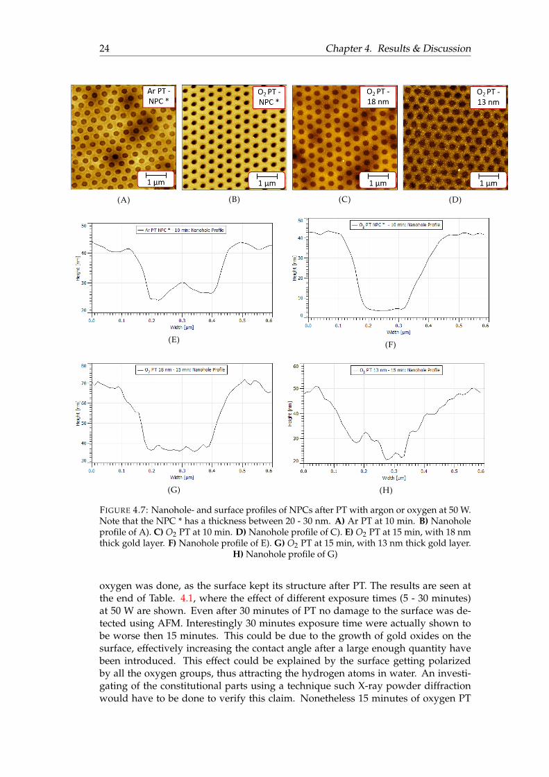
24 Chapter 4. Results & Discussion
(A) (B) (C) (D)
(E) (F)
(G) (H)
FIGURE 4.7: Nanohole- and surface profiles of NPCs after PT with argon or oxygen at 50 W.Note that the NPC * has a thickness between 20 - 30 nm. A) Ar PT at 10 min. B) Nanoholeprofile of A). C) O2 PT at 10 min. D) Nanohole profile of C). E) O2 PT at 15 min, with 18 nmthick gold layer. F) Nanohole profile of E). G) O2 PT at 15 min, with 13 nm thick gold layer.
H) Nanohole profile of G)
oxygen was done, as the surface kept its structure after PT. The results are seen atthe end of Table. 4.1, where the effect of different exposure times (5 - 30 minutes)at 50 W are shown. Even after 30 minutes of PT no damage to the surface was de-tected using AFM. Interestingly 30 minutes exposure time were actually shown tobe worse then 15 minutes. This could be due to the growth of gold oxides on thesurface, effectively increasing the contact angle after a large enough quantity havebeen introduced. This effect could be explained by the surface getting polarizedby all the oxygen groups, thus attracting the hydrogen atoms in water. An investi-gating of the constitutional parts using a technique such X-ray powder diffractionwould have to be done to verify this claim. Nonetheless 15 minutes of oxygen PT
4.3. Plasma Treatment & Hydrophobic Properties 25
seemed very promising and was set as a standard procedure. Unfortunately sam-ples with thinner layers of gold were found damaged by this exposure time. Of thefive thicknesses studied, only 21 nm exhibited no signs of damage to the surface af-ter treatment. In Fig. 4.7C and 4.7D the post-treated surface of 18 and 13 nm goldlayers are seen. The 18 nm samples show a similar damaged wave-like structureas the argon treated sample in Fig. 4.7A, where the 13 nm sample simply seem ex-tremely damaged. This can also be seen from the nanohole profile for each case inFig. 4.7G and 4.7H, where distinct damage to the nanoholes are seen. Regarding the5 and 6 nm samples no surface remained after the PT. A protective gold layer of ade-quate thickness is thus very important to stop the oxygen plasma from reacting withthe PMMA. Some more experiments still need to be done to investigate the effect oflower exposure times and reduced power settings. It is possible that this could leadto discovering treatment procedures for thinner gold layers.
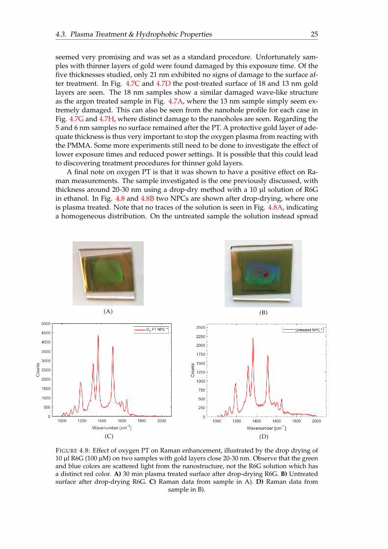
A final note on oxygen PT is that it was shown to have a positive effect on Ra-man measurements. The sample investigated is the one previously discussed, withthickness around 20-30 nm using a drop-dry method with a 10 µl solution of R6Gin ethanol. In Fig. 4.8 and 4.8B two NPCs are shown after drop-drying, where oneis plasma treated. Note that no traces of the solution is seen in Fig. 4.8A, indicatinga homogeneous distribution. On the untreated sample the solution instead spread
(A) (B)
(C) (D)
FIGURE 4.8: Effect of oxygen PT on Raman enhancement, illustrated by the drop drying of10 µl R6G (100 µM) on two samples with gold layers close 20-30 nm. Observe that the greenand blue colors are scattered light from the nanostructure, not the R6G solution which hasa distinct red color. A) 30 min plasma treated surface after drop-drying R6G. B) Untreatedsurface after drop-drying R6G. C) Raman data from sample in A). D) Raman data from
sample in B).
26 Chapter 4. Results & Discussion
very poorly, forming visible clusters of particles as seen in Fig. 4.8B. A compari-son of the two samples were done during a Raman measurement, where the plasmatreated initially showed lower intensity peaks than the untreated one. As the smalldroplet spread extremely well, the question if the surface was properly saturatedhad to be taken into consideration. The experiment was thus redone with an areasimilar to the droplet in Fig. 4.8B. The resulting measurement is seen in relation toan untreated sample in Fig. 4.8C and 4.8D. No negative change in intensity seemto have occurred due to the PT, as clear and similar peaks are seen over the wholespectrum for both cases. The results instead indicate that oxygen PT might provebeneficial for signal enhancement, as a two-fold enhancement is seen. This couldeither be due to the plasma activating the surface or due to the surface being slightlyroughened up —creating new hotspots. A combination of the two is also possible,nonetheless the results look promising.
4.4 Transmittance Data
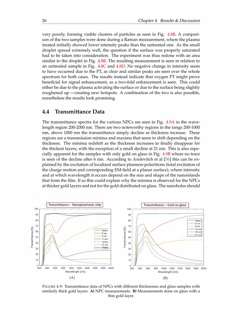
The transmittance spectra for the various NPCs are seen in Fig. 4.9A in the wave-length region 200-2000 nm. There are two noteworthy regions in the range 200-1000nm, above 1000 nm the transmittance simply decline as thickness increase. Theseregions are a transmission minima and maxima that seem to shift depending on thethickness. The minima redshift as the thickness increases to finally disappear forthe thickest layers, with the exception of a small decline at 21 nm. This is also espe-cially apparent for the samples with only gold on glass in Fig. 4.9B where no traceis seen of the decline after 6 nm. According to Axelevitch et al [56] this can be ex-plained by the excitation of localized surface plasmon-polaritions (total excitation ofthe charge motion and corresponding EM-field at a planar surface), where intensityand at which wavelength it occurs depend on the size and shape of the nanoislandsthat form the film. If so this could explain why the minima is observed for the NPCsat thicker gold layers and not for the gold distributed on glass. The nanoholes should
(A) (B)
FIGURE 4.9: Transmittance data of NPCs with different thicknesses and glass samples withsimilarly thick gold layers. A) NPC measurements. B) Measurements done on glass with a
thin gold layer.
4.5. Surface Enhanced Raman Spectroscopy &Fluorescence Measurements
27
theoretically contribute to the plasmonic effect and could as such be a reason for theexistence of the minima. Another reason could be due to using PMMA as a base (thenanogaps where not confined to areas with only nanoholes), effectively creating anenvironment which makes it harder for the gold to form a continuous film. In Fig.4.6 the 18 nm sample still show a surface full of nanogaps, which could still supporthotspots. Nonetheless this minima is a very interesting property, that could poten-tially be used to determine where these samples have their highest plasmonic effect.The maxima on the other hand is explained to be an effect inherent to gold, where itis conditioned by the existence of bulk absorption modes according to their disper-sion equation [56]. Furthermore the extraordinary transmission phenomena is notobserved for the samples at these gold thicknesses, where very similar transmissionare observed with and without nanoholes. The sudden drop in transmitance closeto 200 nm for all samples can be explained by the simple use of glass as a base. Glassis well known to be extremely reflective at short wavelengths [57].
4.5 Surface Enhanced Raman Spectroscopy &Fluorescence Measurements
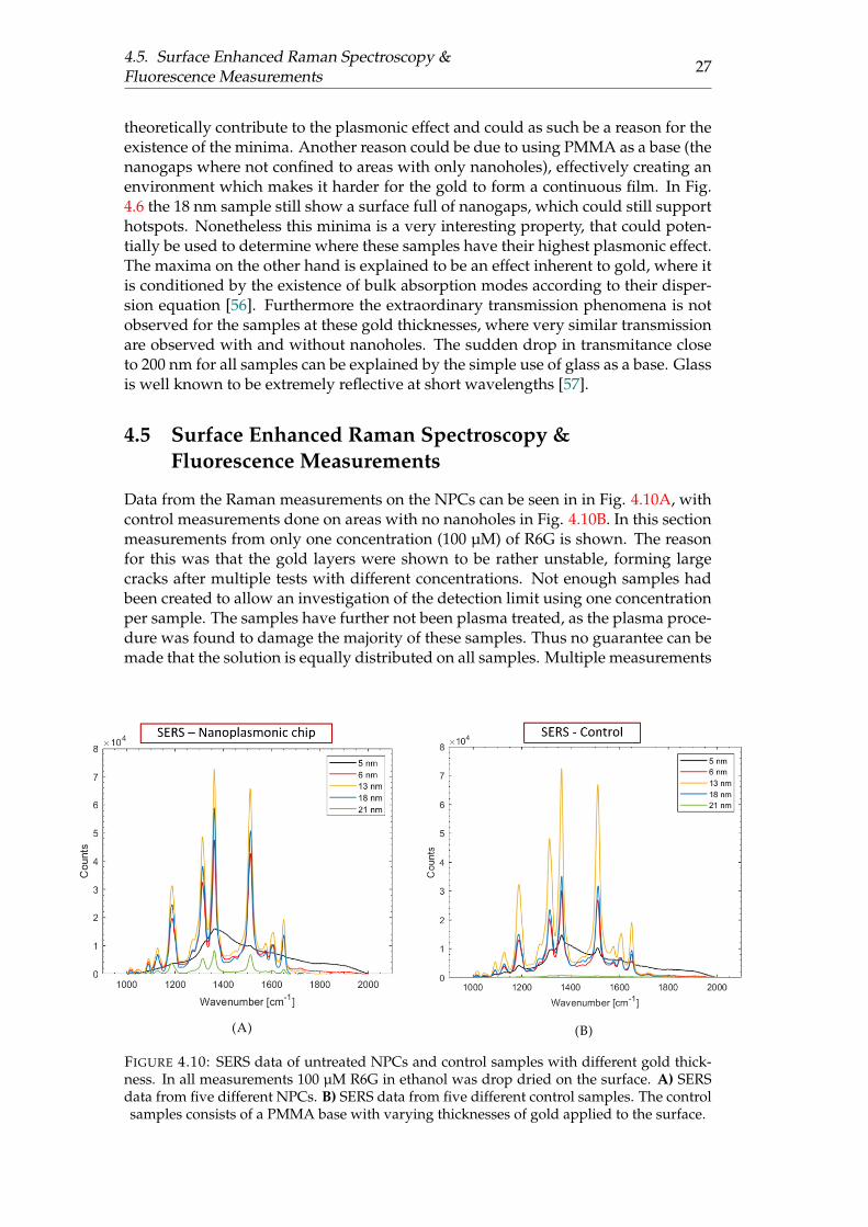
Data from the Raman measurements on the NPCs can be seen in in Fig. 4.10A, withcontrol measurements done on areas with no nanoholes in Fig. 4.10B. In this sectionmeasurements from only one concentration (100 µM) of R6G is shown. The reasonfor this was that the gold layers were shown to be rather unstable, forming largecracks after multiple tests with different concentrations. Not enough samples hadbeen created to allow an investigation of the detection limit using one concentrationper sample. The samples have further not been plasma treated, as the plasma proce-dure was found to damage the majority of these samples. Thus no guarantee can bemade that the solution is equally distributed on all samples. Multiple measurements
(A) (B)
FIGURE 4.10: SERS data of untreated NPCs and control samples with different gold thick-ness. In all measurements 100 µM R6G in ethanol was drop dried on the surface. A) SERSdata from five different NPCs. B) SERS data from five different control samples. The controlsamples consists of a PMMA base with varying thicknesses of gold applied to the surface.
28 Chapter 4. Results & Discussion
were however done on different regions on all samples, where none was found todeviate significantly.
From Fig. 4.10A it is quite clear that the gold thickness plays an important rolefor Raman signal enhancement. There seem to be a region between 6 - 18 nm wherethe most intense Raman scattering are measured, with a maximum around 13 nm.The reason for this could be explained from Fig. 4.6 where evidence of the goldssurface morphology can be seen. At 5 nm the surface is still very patchy, creatinga very inhomogeneous environment where scattered noise dominate. At 6 nm it ispossible to see some grainy structure, which could be a sign of metallic nanoislandsdistributed on the surface. As these generate hotspots in their vicinity an enhancedRaman scattering is observed. The many nanogaps in Fig. 4.6C seems to generateeven stronger hotspots, as the strongest signal from all samples is observed here. At18 nm less nanogaps are visible, which could explain the reduction in signal. Finallyat 21 nm a very low signal is observed, which could be attributed to the loss of thesenanogap hotspots as seen in Fig. 4.6E. When comparing the nanohole array to thesimple surface of gold distributed on PMMA in Fig. 4.10B, some interesting effectsare seen. It seems as if the nanoholes in general are beneficial for signal enhance-ment, where the strongest enhancements are observed for thicker samples. Withvery thin layers they stop contributing as significantly, where the enhancement at 6nm is less then at 18 nm for instance. Even at 5 nm it is possible to observe moredistinct peaks in the noise of the control sample, than on the NPC. At 13 nm themeasured signals from both control and NPC are interestingly enough found to beextremely similar. It seems as if a surface containing only these specific nanogapsyield the same enhancement as one with nanogaps and nanoholes. At this specificthickness the nanoholes yield no boost in Raman signal, or is simply dominated bythe nanogap effect.
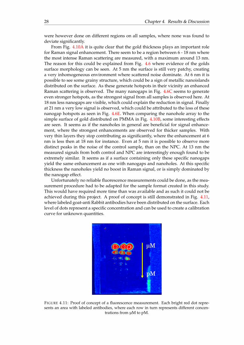
Unfortunately no reliable fluorescence measurements could be done, as the mea-surement procedure had to be adapted for the sample format created in this study.This would have required more time than was available and as such it could not beachieved during this project. A proof of concept is still demonstrated in Fig. 4.11,where labeled goat-anti Rabbit antibodies have been distributed on the surface. Eachlevel of dots represent a specific concentration and can be used to create a calibrationcurve for unknown quantities.
FIGURE 4.11: Proof of concept of a fluorescence measurement. Each bright red dot repre-sents an area with labeled antibodies, where each row in turn represents different concen-
trations from µM to pM.
4.6. Scaling Up - Nanoimprinting Lithography 29
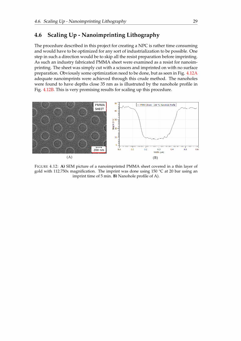
4.6 Scaling Up - Nanoimprinting Lithography
The procedure described in this project for creating a NPC is rather time consumingand would have to be optimized for any sort of industrialization to be possible. Onestep in such a direction would be to skip all the resist preparation before imprinting.As such an industry fabricated PMMA sheet were examined as a resist for nanoim-printing. The sheet was simply cut with a scissors and imprinted on with no surfacepreparation. Obviously some optimization need to be done, but as seen in Fig. 4.12Aadequate nanoimprints were achieved through this crude method. The nanoholeswere found to have depths close 35 nm as is illustruted by the nanohole profile inFig. 4.12B. This is very promising results for scaling up this procedure.
(A) (B)
FIGURE 4.12: A) SEM picture of a nanoimprinted PMMA sheet covered in a thin layer ofgold with 112.750x magnification. The imprint was done using 150 °C at 20 bar using an
imprint time of 5 min. B) Nanohole profile of A).

31
Chapter 5
Conclusions
Both PMMA and HPC turned out to be good resists for soft nanoimprinting lithog-raphy, as excellent nanoimprints were achieved on both resists. HPC proved inad-equate for the purpose of this project as it dissolved to easily in any water-basedfluid. This could however be useful in a nanopillar fabrication procedure, where thenanohole imprinted HPC could be used as a template.
Temperature was further found to be a key parameter for nanoimprint lithog-raphy on PMMA. It not only affected the shape of the nanoholes, but also theirdepths. Pressure and time proved less vital, as they could be varied significantlywithout altering the imprints in a major way. The nanoholes were also shown tokeep their structure when a thin gold layer was applied by evaporation. The goldssurface morphology (nanoislands, nanogaps or continuous film) did however no-ticeably change depending on the amount of mass evaporated. All samples initiallydisplayed hydrophobic properties, including samples such as PMMA and nanoim-printed PMMA. PT were however shown to be a viable method to increase the hy-drophilicity of all samples, using either argon or oxygen. Oxygen PT was found todamage the NPCs surface less than when using argon at certain thicknesses. Careshould be taken with the exposure time and power settings, as oxygen was shownto damage samples with very thin gold layers. PT could also prove beneficial forRaman signal enhancement, as a two-fold enhancement was observed in an exper-iment. The gold thickness was also found to greatly affect the Raman scattering,with a maximum intensity observed at 13 nm. This was attributed to the surfacestructure, where a surface including grains and nanogaps were favorable. In gen-eral the nanoholes proved beneficial for enhancing the signal, with an exception at13 nm. This effect could be explained by very favorable nanogaps in the gold sur-face, hosting a surplus of hotsposts which dominate the nanoholes effect. Two effectswere further noticeable when analyzing the transmittance, an inherent transmittancemaxima of gold —that blue- or redshifted depending on the thickness— and a trans-mittance minima which is associated to the excitation of localized surface plasmon-polaritons. This minima further vanishes for thicker films, where the structure haschanged to a more continuous film —loosing its hotspots in the process. This wasmore apparent for gold on glass, then for the NPCs where the minima was foundto exist at thicker films. This could be due to the hotspots around the nanoholes, ordue to an environmental aspect of the PMMA —which inhibit the creation of a morecontinuous film of gold. Furthermore a method for scaling up the nanoimpritingprocedure, using industry fabricated PMMA sheets was proposed.
In general the project proved a success, where a method for developing NPCsusing nanoimprinting lithography and evaporation was properly optimized. Theeffect of nanoholes were also shown to generally be beneficial for Raman scattering,where the enhancement factor was found to depend on the gold thickness. Morework needs to be done however, as many parts can still be further improved.
32 Chapter 5. Conclusions
5.1 Future Work
For future work plenty of intriguing directions are available to take. It could forinstance be of great interest to examine the enhancement effect after depositingnanoparticles of various sizes on the surface. These should theoretically boost thesignal even further, since more LSPR locations are introduced. Also as the fluores-cence part of this project could not be finalized, more time need to be spend onfinishing these measurements for varying gold thicknesses. The stability of the chipcould also need some improvement, perhaps by adding a bonding layer of titaniumor chromium before depositing the gold. More work is also needed to optimize thePT for the thinner gold layers, subsequently analyzing their performance regardingfluorescence and SERS. Similarly the parameters for imprinting on PMMA sheetsneeds to be further improved, including all the follow-up work that was done forthe NPCs in this project. Finally an investigating of the possibilities for integratingthe NPC into a microfluidic device could be started, with the end goal of developinga proper diagnostic system.

33
Bibliography
[1] World Health Organization. “World health statistics 2018: monitoring healthfor the SDGs, sustainable development goals.” In: Geneva, 2018.
[2] K. Hanada, A. Okazaki, N. Hirano, Y. Izumi, T. Minami, J. Ikemoto, K. Kane-mitsu and F. Hino. “Effective screening for early diagnosis of pancreatic can-cer”. In: Best Practice & Research Clinical Gastroenterology 29.6 (2015). Cancerscreening and prevention in Asia, pp. 929–939.
[3] B. Zhang, B. A. Pinsky, J. S. Ananta, S. Zhao, S. Arulkumar, H. Wan, M. K. Sa-hoo, J. Abeynayake, J. J. Waggoner, C. Hopes, M. Tang and H. Dai. “Diagnosisof Zika virus infection on a nanotechnology platform”. In: Nature Medicine 23(2017), pp. 548–550.
[4] S. M. Fothergill, C. Joyce and F. Xie. “Metal enhanced fluorescence biosensing:from ultra-violet towards second near-infrared window”. In: Nanoscale 10 (452018), pp. 20914–20929.
[5] S. Srivastava, P. K. Singh, V. Vatsalya and R. C. Karch. “Developments in theDiagnostic Techniques of Infectious Diseases: Rural and Urban Prospective.”In: Advances in infectious diseases 8 (2018), pp. 121–1387.
[6] X. Li, M. Soler, C. I. Özdemir, A. Belushkin, F. Yesilköy and H. Altug. “Plas-monic nanohole array biosensor for label-free and real-time analysis of livecell secretion”. In: Lab Chip 17 (13 2017), pp. 2208–2217.
[7] J. A. Goode, J. V. H. Rushworth and P. A. Millner. “Biosensor Regeneration:A Review of Common Techniques and Outcomes”. In: Langmuir 31.23 (2014),pp. 6267–6276.
[8] S. Sang, Y. Wang, Q. Feng, Y. Wei, J. Ji and W. Zhang. “Progress of new label-free techniques for biosensors: a review”. In: Critical Reviews in Biotechnology36.3 (2016), pp. 465–481.
[9] H. Nguyen, J. Park, S. Kang and M. Kim. “Surface Plasmon Resonance: AVersatile Technique for Biosensor Applications”. In: Sensors 15.5 (May 2015),pp. 10481–10510.
[10] M. Soler, A. Belushkin, A. Cavallini, C. Kebbi-Beghdadi, G. Greub and H. Al-tug. “Multiplexed nanoplasmonic biosensor for one-step simultaneous detec-tion of Chlamydia trachomatis and Neisseria gonorrhoeae in urine”. In: Biosen-sors and Bioelectronics 94 (2017), pp. 560–567.
[11] K. L. Lee, M. L. You, C. H. Tsai, E. H. Lin, S. Y. Hsieh, M. H. Ho, J. C. Hsu andP. K. Wei. “Nanoplasmonic biochips for rapid label-free detection of imidaclo-prid pesticides with a smartphone”. In: Biosensors and Bioelectronics 75 (2016),pp. 88–95.
[12] A. A. Yanik, M. Huang, O. Kamohara, A. Artar, T. W. Geisbert, J. H. Connorand H. Altug. “An Optofluidic Nanoplasmonic Biosensor for Direct Detectionof Live Viruses from Biological Media”. In: Nano Letters 10.12 (2010), pp. 4962–4969.

34 BIBLIOGRAPHY
[13] S. H. Lee, N. C. Lindquist, N. J. Wittenberg, L. R. Jordan and S. H. Oh. “Real-time full-spectral imaging and affinity measurements from 50 microfluidicchannels using nanohole surface plasmon resonance”. In: Lab Chip 12 (20 2012),pp. 3882–3890.
[14] A. Fanget, F. Traversi, S. Khlybov, P. Granjon, A. Magrez, L. Forró and A. Rade-novic. “Nanopore Integrated Nanogaps for DNA Detection”. In: Nano Letters14.1 (2014), pp. 244–249.
[15] I. Hyungsoon, H. Shao, Y. I. Park, V. M. Peterson, C. M. Castro, R. Weisslederand H. Lee. “Label-free detection and molecular profiling of exosomes with anano-plasmonic sensor.” In: Nature biotechnology 32.5 (2014), pp. 490–495.
[16] T. W. Ebbesen, H. J. Lezec, H. F. Ghaemi, T. Thio and P. A. Wolff. “Extraordi-nary optical transmission through sub-wavelength hole arrays”. In: NatureSP391 (Feb. 1998), pp. 667–669.
[17] L. Tu, W. Wang and Q. Zhichang. “Review of Extraordinary Optical Transmis-sion: Theory and Application in Biochemical Analysis”. In: Spectroscopy andSpectral Analysis 35 (Mar. 2015), pp. 751–759.
[18] D. Correia-Ledo, K. F. Gibson, A. Dhawan, M. Couture, T. Vo-Dinh, D. Grahamand J. F. Masson. “Assessing the Location of Surface Plasmons Over Nanotri-angle and Nanohole Arrays of Different Size and Periodicity”. In: The Journalof Physical Chemistry C 116.12 (2012), pp. 6884–6892.
[19] C. Dore, J. Osmond and A. Mihi. “A water-processable cellulose-based resistfor advanced nanofabrication”. In: Nanoscale 10 (37 2018), pp. 17884–17892.
[20] R. G. Hill. “10 - Biomedical polymers”. In: Biomaterials, Artificial Organs and Tis-sue Engineering. Woodhead Publishing Series in Biomaterials. Woodhead Pub-lishing, 2005, pp. 97–106.
[21] N. Metzler, K. Dantonello, M. Roßmeier, M. Bauer, S. Horn and M. Kupke.“Influence of Plasma activation on surface energy and adhesive properties ofRTM6-CFRP”. In: Journal Of Materials Science and Surface Engineering 4 (Dec.2016), pp. 472–482.
[22] K. M. Mayer and J. H. Hafner. “Localized Surface Plasmon Resonance Sen-sors”. In: Chemical Reviews 111.6 (2011), pp. 3828–3857.
[23] K. A. Willets and R. P. Van Duyne. “Localized Surface Plasmon ResonanceSpectroscopy and Sensing”. In: Annual Review of Physical Chemistry 58.1 (2007),pp. 267–297.
[24] E. Petryayeva and U. J. Krull. “Localized surface plasmon resonance: Nanos-tructures, bioassays and biosensing—A review”. In: Analytica Chimica Acta706.1 (2011), pp. 8–24.
[25] Cytodiagnostics - Gold Nanoparticle Properties. Accessed: 2019-08-05. URL: http://www.cytodiagnostics.com/store/pc/viewcontent.asp?idpage=2.
[26] E. C. Le Ru and P. G. Etchegoin. “Chapter 2 - Raman spectroscopy and re-lated optical techniques”. In: Principles of Surface-Enhanced Raman Spectroscopy.Amsterdam: Elsevier, 2009, pp. 29–120.
[27] C. D. Geddes and J. Lakowicz. “Metal-Enhanced Fluorescence”. In: Journal ofFluorescence 12 (June 2002), pp. 121–129.
[28] U. K. Sur. “Surface-enhanced Raman spectroscopy - Recent Advancement ofRaman Spectroscopy”. In: Resonance 15.2 (2010), pp. 154–164.
BIBLIOGRAPHY 35
[29] C. L. Haynes, A. D. McFarland and R. P. Van Duyne. “Surface-Enhanced Ra-man Spectroscopy”. In: Analytical Chemistry 77.17 (2005), 338 A–346 A.
[30] E. C. Le Ru and P. G. Etchegoin. “Chapter 4 - SERS enhancement factors andrelated topics”. In: Principles of Surface-Enhanced Raman Spectroscopy. Amster-dam: Elsevier, 2009, pp. 185–264.
[31] P. L. Stiles, J. A. Dieringer, N. C. Shah and R. P. Van Duyne. “Surface-EnhancedRaman Spectroscopy”. In: Annual Review of Analytical Chemistry 1.1 (2008),pp. 601–626.
[32] K. Aslan, I. Gryczynski, J. Malicka, E. Matveeva, J. R. Lakowicz and C. D. Ged-des. “Metal-enhanced fluorescence: an emerging tool in biotechnology”. In:Current Opinion in Biotechnology 16.1 (2005). Analytical biotechnology, pp. 55–62.
[33] Clean Air Technology - What is a Cleanroom ? Accessed: 2019-08-14. URL: https://www.cleanairtechnology.com/what-is-a-cleanroom.php.
[34] A. Baptista, F. Silva, J. Porteiro, J. Míguez and G. Pinto. “Sputtering PhysicalVapour Deposition (PVD) Coatings: A Critical Review on Process Improve-ment and Market Trend Demands”. In: Coatings 8.11 (2018).
[35] C. Dwivedi, I. Pandey, H. Pandey, P. W. Ramteke, A. C. Pandey, S. B. Mishraand S. Patil. “Chapter 9 - Electrospun Nanofibrous Scaffold as a Potential Car-rier of Antimicrobial Therapeutics for Diabetic Wound Healing and TissueRegeneration”. In: Nano- and Microscale Drug Delivery Systems. Elsevier, 2017,pp. 147–164.
[36] A. T. Luís, D. Hlúbiková, V. Vaché, P. Choquet, L. Hoffmann and L. Ector.“Atomic force microscopy (AFM) application to diatom study: review and per-spectives”. In: Journal of Applied Phycology 29.6 (2017), pp. 2989–3001.
[37] V. J. Morris, A. R. Kirby and A. P. Gunning. “Chapter 3 -Atomic Force Mi-croscopy for Biologists”. In: Atomic Force Microscopy for Biologists. Singapore:Imperial College Press, 2009, pp. 41–75.
[38] S. Liu and Y. Wang. “Application of AFM in microbiology: a review”. In: Scan-ning 32.2 (2010), pp. 61–73.
[39] V. J. Morris, A. R. Kirby and A. P. Gunning. “Chapter 2 -Atomic Force Mi-croscopy for Biologists”. In: Atomic Force Microscopy for Biologists. Singapore:Imperial College Press, 2009, pp. 5–40.
[40] D. T. W. Toolan and J. R. Howse. “Development of in situ studies of spin coatedpolymer films”. In: J. Mater. Chem. C 1 (4 2013), pp. 603–616.
[41] M. Boratto. “Semiconducting and Insulating oxides applied to electronic de-vices”. PhD thesis. Feb. 2018.
[42] S. Ebnesajjad and C. Ebnesajjad. “Chapter 1 - Introduction to Surface Prepara-tion”. In: Surface Treatment of Materials for Adhesive Bonding. Norwich: ElsevierScience & Technology Books, 2013, pp. 3–6.
[43] S. Ebnesajjad and C. Ebnesajjad. “Chapter 9 - Plasma Treatment of PolymericMaterials”. In: Surface Treatment of Materials for Adhesive Bonding. Norwich: El-sevier Science & Technology Books, 2013, pp. 227–269.
[44] M. Yamamoto, T. Matsumae, Y. Kurashima, H. Takagi, T. Suga, T. Itoh andE. Higurashi. “Comparison of Argon and Oxygen Plasma Treatments for Am-bient Room-Temperature Wafer-Scale Au–Au Bonding Using Ultrathin AuFilms”. In: Micromachines 10.2 (2019).
36 BIBLIOGRAPHY
[45] A. Mohammed and A. Abdullah. “Scanning Electron Microscopy (SEM): AReview”. In: Jan. 2019.
[46] K. D. Vernon-Parry. “Scanning electron microscopy: an introduction”. In: III-Vs Review 13.4 (2000), pp. 40–44.
[47] Scanning Electron Microscope A To Z - Basic Knowledge For Using The SEM. Ac-cessed: 2019-08-05. URL: https://www.jeol.co.jp/en/applications/pdf/sm/sem_atoz_all.pdf.
[48] National University of Singapore - Clean Room. Accessed: 2019-08-10. URL:https://gc.science.nus.edu.sg/content/clean-room.
[49] Obducat - Eitre 3. Accessed: 2019-08-10. URL: https://www.obducat.com/products/product-portfolio/product/eitrer-3/.
[50] Kurt J. Lesker - Physical Vapor Deposition Systems. Accessed: 2019-08-10. URL:https : / / www . lesker . com / newweb / ped / physical - vapor - deposition -systems.cfm.
[51] RITM Industry - Plasma Surface Preparation Machines. Accessed: 2019-08-10.URL: http://ritmindustry.com/catalog/plasma-surface-preparation-machines/plasma-surface-treatment-machine-laboratory-2/.
[52] The University of Kansas, IBER - Surface Characterization. Accessed: 2019-08-10.URL: https://berc.ku.edu/surfacae-characterization.
[53] D. R. Barbero, M. S. M. Saifullah, P. Hoffmann, H. J. Mathieu, D. Anderson, G.A. C. Jones, M. E. Welland and U. Steiner. “High-Resolution Nanoimprintingwith a Robust and Reusable Polymer Mold”. In: Advanced Functional Materials17.14 (2007), pp. 2419–2425.
[54] R. P. Kusy, W. F. Simmons and A. R. Greenberg. “Glass transition temperatureof poly(methyl methacrylate) blends”. In: Polymer 22.2 (1981), pp. 268–270.
[55] W. E. Smith and C. Rodger. “Surface-Enhanced Raman Scattering (SERS), Ap-plications”. In: Encyclopedia of Spectroscopy and Spectrometry. Second Edition.Oxford: Academic Press, 1999, pp. 2822–2827.
[56] A. Axelevitch, B. Apter and G. Golan. “Simulation and experimental inves-tigation of optical transparency in gold island films”. In: Optics Express 21.4(2013), pp. 4126–4138.
[57] I. Duarte, A. Malvestiti and S. Mariana. “The role of glass as a barrier againstthe transmission of ultraviolet radiation: an experimental study”. In: Photoder-matology, Photoimmunology & Photomedicine 25.4 (2009), pp. 181–184.