물리적 분자 제어 조작 ( nanoplasmonic optical tweezers)
DESCRIPTION
물리적 분자 제어 조작 ( nanoplasmonic optical tweezers). 지스트 이용구. Conventional optical tweezers. - PowerPoint PPT PresentationTRANSCRIPT
물리적 분자 제어 조작(nanoplasmonic optical tweezers)
지스트 이용구
Conventional optical tweez-ers
• Consider an object of radius R much smaller than the wavelength of the incident trapping light (known as the Rayleigh regime). Reduc-ing the size of the object causes two main ef -fects that both work against stable trapping.
• First, the magnitude of the restoring force decreases abruptly (following an R3 law), which results in a shallower trapping well.
• Second, the damping of the trapped speci-men decreases because of a reduction in vis-cous drag.
Mathieu L. Juan, Maurizio Righini and Romain Quidant, Plasmon nano-optical tweezers, Nature Photonics, Vol. 5, pp. 349, 2011

Evanescent wave• An evanescent wave is a
near-field standing wave with an intensity that ex-hibits exponential decay with distance from the boundary at which the wave was formed.
• They are formed at the boundary between two me-dia with different wave mo-tion properties, and are most intense within one third of a wavelength from the surface of formation.
http://www.olympusmicro.com/primer/techniques/fluorescence/tirf/tirfintro.html
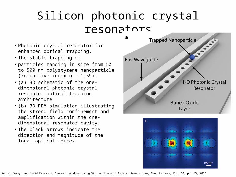
Silicon photonic crystal resonators• Photonic crystal resonator for en-
hanced optical trapping. • The stable trapping of• particles ranging in size from 50 to
500 nm polystyrene nanoparticle (refractive index n = 1.59).
• (a) 3D schematic of the one-di-mensional photonic crystal res-onator optical trapping architecture
• (b) 3D FEM simulation illustrating the strong field confinement and amplification within the one-di-mensional resonator cavity.
• The black arrows indicate the di-rection and magnitude of the local optical forces.
Sudeep Mandal, Xavier Serey, and David Erickson, Nanomanipulation Using Silicon Photonic Crystal Resonatorsm, Nano Letters, Vol. 10, pp. 99, 2010
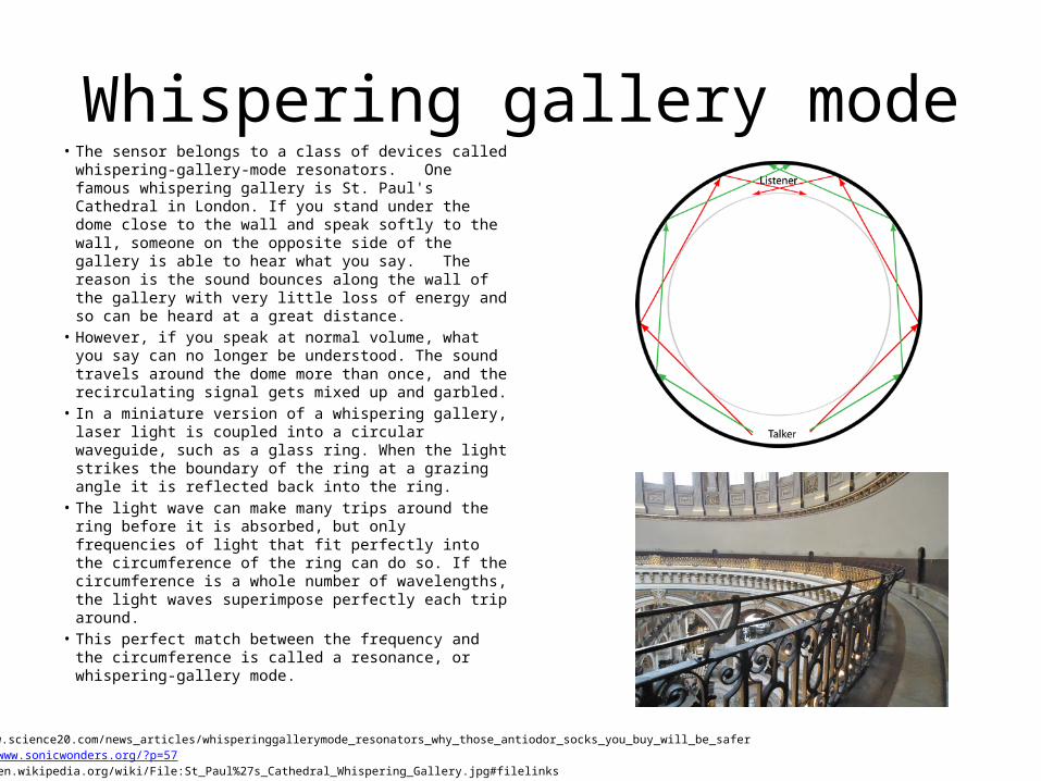
Whispering gallery mode• The sensor belongs to a class of devices called
whispering-gallery-mode resonators. One famous whispering gallery is St. Paul's Cathedral in Lon-don. If you stand under the dome close to the wall and speak softly to the wall, someone on the op-posite side of the gallery is able to hear what you say. The reason is the sound bounces along the wall of the gallery with very little loss of energy and so can be heard at a great distance.
• However, if you speak at normal volume, what you say can no longer be understood. The sound trav-els around the dome more than once, and the re-circulating signal gets mixed up and garbled.
• In a miniature version of a whispering gallery, laser light is coupled into a circular waveguide, such as a glass ring. When the light strikes the boundary of the ring at a grazing angle it is re-flected back into the ring.
• The light wave can make many trips around the ring before it is absorbed, but only frequencies of light that fit perfectly into the circumference of the ring can do so. If the circumference is a whole number of wavelengths, the light waves superim-pose perfectly each trip around.
• This perfect match between the frequency and the circumference is called a resonance, or whisper-ing-gallery mode.
http://www.science20.com/news_articles/whisperinggallerymode_resonators_why_those_antiodor_socks_you_buy_will_be_saferhttp://www.sonicwonders.org/?p=57http://en.wikipedia.org/wiki/File:St_Paul%27s_Cathedral_Whispering_Gallery.jpg#filelinks
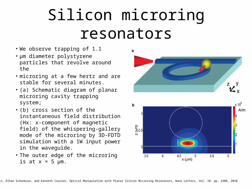
Silicon microring resonators• We observe trapping of 1.1• μm diameter polystyrene parti-
cles that revolve around the• microring at a few hertz and are
stable for several minutes.• (a) Schematic diagram of planar
microring cavity trapping system; • (b) cross section of the instanta-
neous field distribution (Hx: x-component of magnetic field) of the whispering-gallery mode of the microring by 3D-FDTD simu-lation with a 1W input power in the waveguide.
• The outer edge of the microring is at x ≈ 5 μm.
Shiyun Lin, Ethan Schonbrun, and Kenneth Crozier, Optical Manipulation with Planar Silicon Microring Resonators, Nano Letters, Vol. 10. pp. 2408, 2010
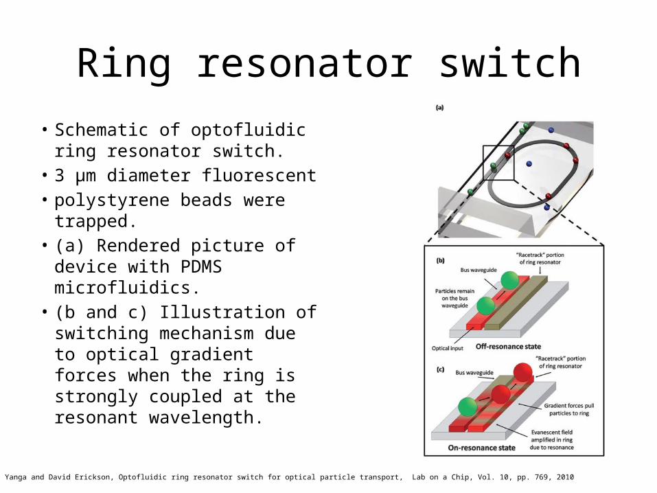
Ring resonator switch• Schematic of optofluidic ring
resonator switch. • 3 μm diameter fluorescent• polystyrene beads were
trapped.• (a) Rendered picture of de-
vice with PDMS microflu-idics.
• (b and c) Illustration of switching mechanism due to optical gradient forces when the ring is strongly coupled at the resonant wavelength.
Allen H. J. Yanga and David Erickson, Optofluidic ring resonator switch for optical particle transport, Lab on a Chip, Vol. 10, pp. 769, 2010
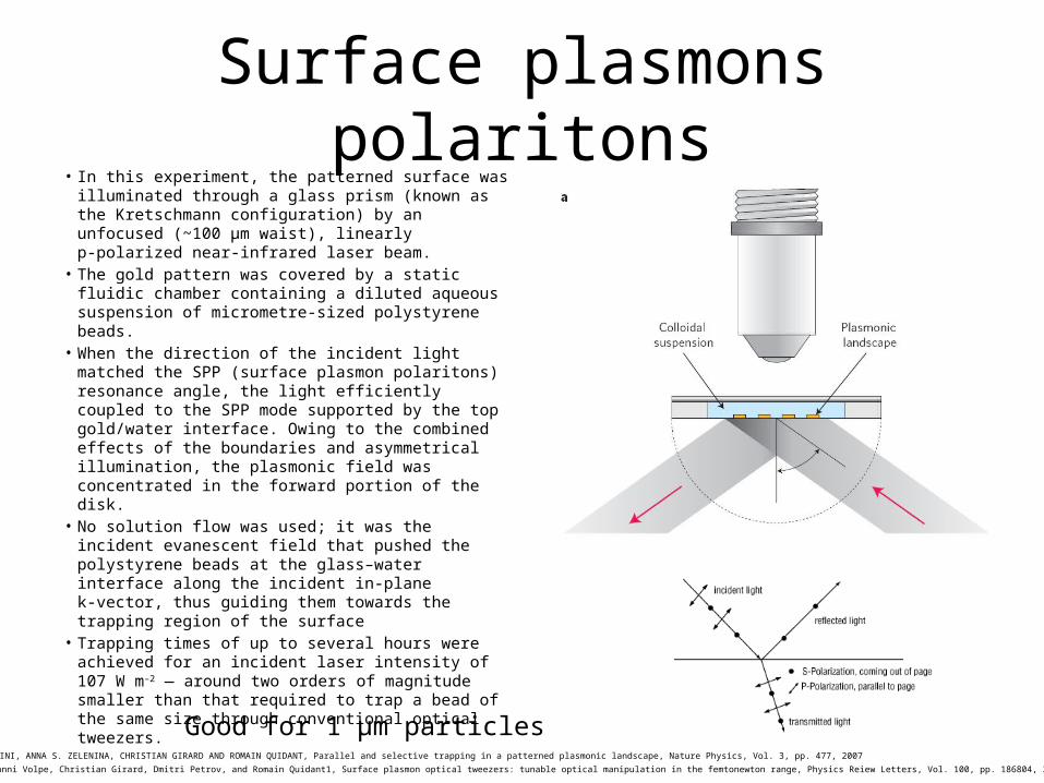
Surface plasmons polaritons• In this experiment, the patterned surface was
illuminated through a glass prism (known as the Kretschmann configuration) by an unfo-cused (~100 μm waist), linearly p‑polarized near-infrared laser beam.
• The gold pattern was covered by a static fluidic chamber containing a diluted aqueous suspen-sion of micrometre-sized polystyrene beads.
• When the direction of the incident light matched the SPP (surface plasmon polaritons) resonance angle, the light efficiently coupled to the SPP mode supported by the top gold/wa-ter interface. Owing to the combined effects of the boundaries and asymmetrical illumination, the plasmonic field was concentrated in the forward portion of the disk.
• No solution flow was used; it was the incident evanescent field that pushed the polystyrene beads at the glass–water interface along the incident in-plane k‑vector, thus guiding them towards the trapping region of the surface
• Trapping times of up to several hours were achieved for an incident laser intensity of 107 W m–2 — around two orders of magnitude smaller than that required to trap a bead of the same size through conventional optical tweez-ers. Good for 1 μm particles
Maurizio Righini, Giovanni Volpe, Christian Girard, Dmitri Petrov, and Romain Quidant1, Surface plasmon optical tweezers: tunable optical manipulation in the femtonewton range, Physics Reiew Letters, Vol. 100, pp. 186804, 2008MAURIZIO RIGHINI, ANNA S. ZELENINA, CHRISTIAN GIRARD AND ROMAIN QUIDANT, Parallel and selective trapping in a patterned plasmonic landscape, Nature Physics, Vol. 3, pp. 477, 2007
Field enhancement at sharply point metal tip under laser illumi-
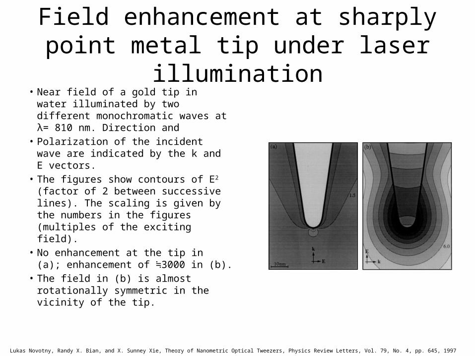
nation• Near field of a gold tip in water il-
luminated by two different monochromatic waves at λ= 810 nm. Direction and
• Polarization of the incident wave are indicated by the k and E vec-tors.
• The figures show contours of E2 (factor of 2 between successive lines). The scaling is given by the numbers in the figures (multiples of the exciting field).
• No enhancement at the tip in (a); enhancement of ≒3000 in (b).
• The field in (b) is almost rotation-ally symmetric in the vicinity of the tip.
Lukas Novotny, Randy X. Bian, and X. Sunney Xie, Theory of Nanometric Optical Tweezers, Physics Review Letters, Vol. 79, No. 4, pp. 645, 1997
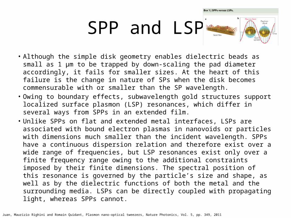
SPP and LSP• Although the simple disk geometry enables dielectric beads as small
as 1 μm to be trapped by down-scaling the pad diameter accordingly, it fails for smaller sizes. At the heart of this failure is the change in nature of SPs when the disk becomes commensurable with or smaller than the SP wavelength.
• Owing to boundary effects, subwavelength gold structures support lo-calized surface plasmon (LSP) resonances, which differ in several ways from SPPs in an extended film.
• Unlike SPPs on flat and extended metal interfaces, LSPs are associ-ated with bound electron plasmas in nanovoids or particles with di-mensions much smaller than the incident wavelength. SPPs have a continuous dispersion relation and therefore exist over a wide range of frequencies, but LSP resonances exist only over a finite frequency range owing to the additional constraints imposed by their finite di-mensions. The spectral position of this resonance is governed by the particle’s size and shape, as well as by the dielectric functions of both the metal and the surrounding media. LSPs can be directly coupled with propagating light, whereas SPPs cannot.
Mathieu L. Juan, Maurizio Righini and Romain Quidant, Plasmon nano-optical tweezers, Nature Photonics, Vol. 5, pp. 349, 2011
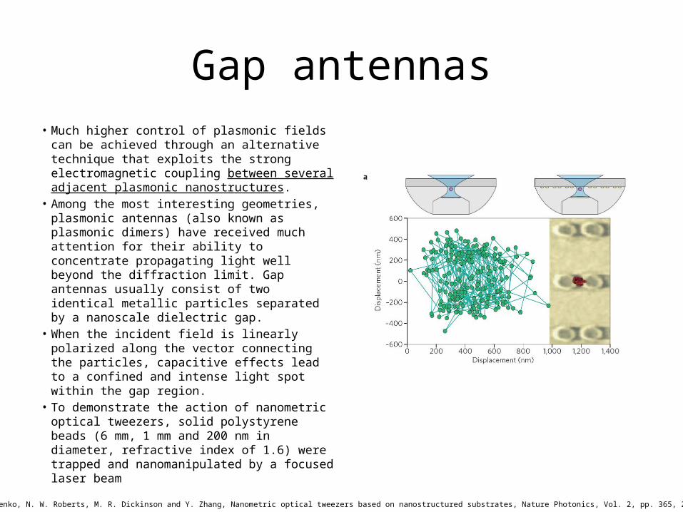
Gap antennas• Much higher control of plasmonic fields
can be achieved through an alternative technique that exploits the strong elec-tromagnetic coupling between several adjacent plasmonic nanostructures.
• Among the most interesting geometries, plasmonic antennas (also known as plasmonic dimers) have received much attention for their ability to concentrate propagating light well beyond the diffrac-tion limit. Gap antennas usually consist of two identical metallic particles separated by a nanoscale dielectric gap.
• When the incident field is linearly polar-ized along the vector connecting the par-ticles, capacitive effects lead to a con-fined and intense light spot within the gap region.
• To demonstrate the action of nanometric optical tweezers, solid polystyrene beads (6 mm, 1 mm and 200 nm in diameter, refractive index of 1.6) were trapped and nanomanipulated by a focused laser beamA. N. Grigorenko, N. W. Roberts, M. R. Dickinson and Y. Zhang, Nanometric optical tweezers based on nanostructured substrates, Nature Photonics, Vol. 2, pp. 365, 2011
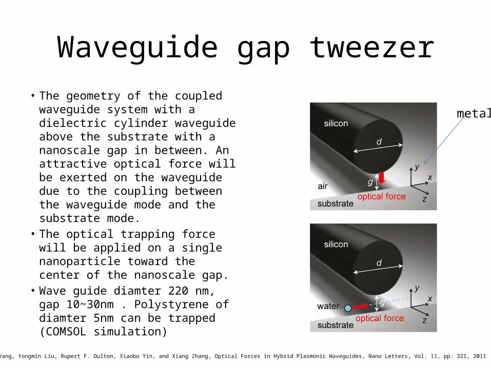
Waveguide gap tweezer• The geometry of the coupled
waveguide system with a di-electric cylinder waveguide above the substrate with a nanoscale gap in between. An attractive optical force will be exerted on the waveguide due to the coupling between the waveguide mode and the sub-strate mode.
• The optical trapping force will be applied on a single nanopar-ticle toward the center of the nanoscale gap.
• Wave guide diamter 220 nm, gap 10~30nm . Polystyrene of diamter 5nm can be trapped (COMSOL simulation)
Xiaodong Yang, Yongmin Liu, Rupert F. Oulton, Xiaobo Yin, and Xiang Zhang, Optical Forces in Hybrid Plasmonic Waveguides, Nano Letters, Vol. 11, pp. 321, 2011
metal
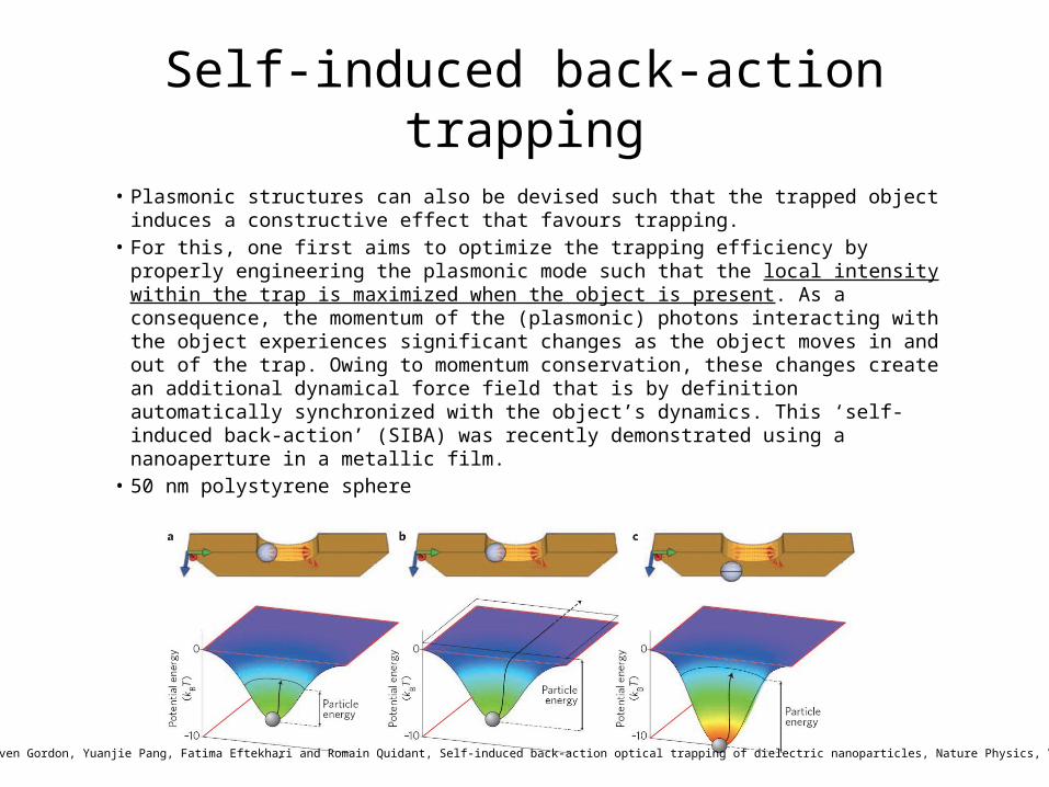
Self-induced back-action trapping• Plasmonic structures can also be devised such that the trapped object in-
duces a constructive effect that favours trapping.• For this, one first aims to optimize the trapping efficiency by properly engi-
neering the plasmonic mode such that the local intensity within the trap is maximized when the object is present. As a consequence, the momentum of the (plasmonic) photons interacting with the object experiences signifi-cant changes as the object moves in and out of the trap. Owing to momen-tum conservation, these changes create an additional dynamical force field that is by definition automatically synchronized with the object’s dynamics. This ‘self-induced back-action’ (SIBA) was recently demonstrated using a nanoaperture in a metallic film.
• 50 nm polystyrene sphere
Mathieu L. Juan, Reuven Gordon, Yuanjie Pang, Fatima Eftekhari and Romain Quidant, Self-induced back-action optical trapping of dielectric nanoparticles, Nature Physics, Vol. 5, pp. 915, 2009
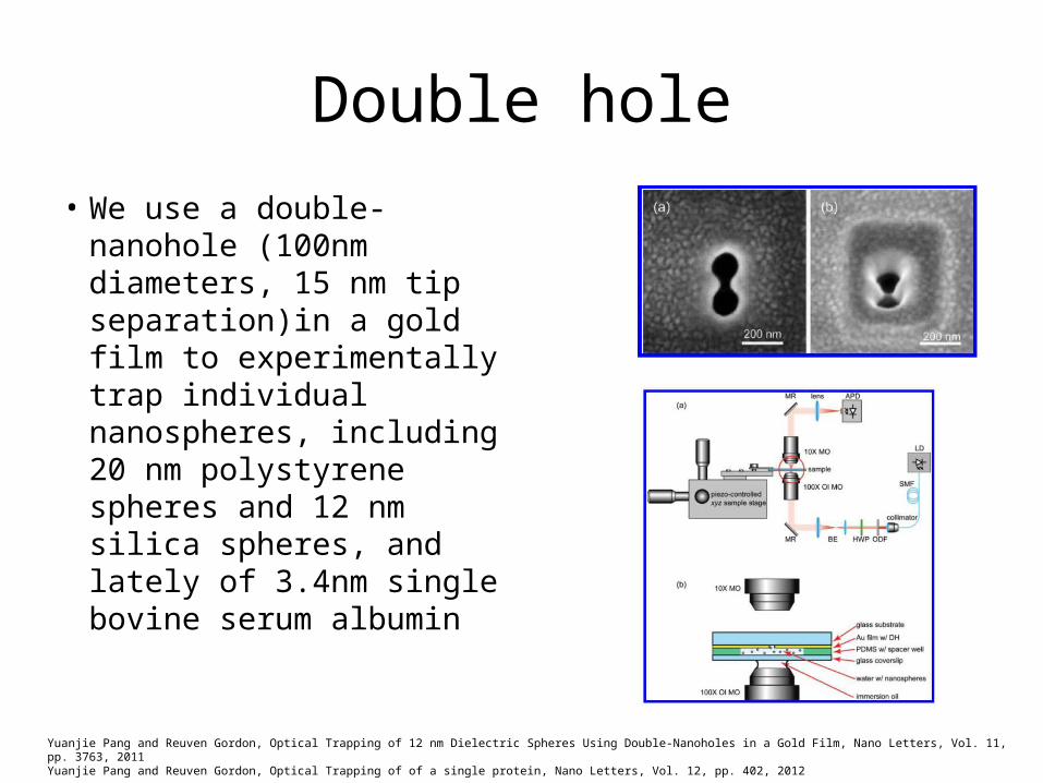
Double hole• We use a double-
nanohole (100nm di-ameters, 15 nm tip separation)in a gold film to experimentally trap individual nanospheres, including 20 nm polystyrene spheres and 12 nm sil-ica spheres, and lately of 3.4nm single bovine serum albumin
Yuanjie Pang and Reuven Gordon, Optical Trapping of 12 nm Dielectric Spheres Using Double-Nanoholes in a Gold Film, Nano Letters, Vol. 11, pp. 3763, 2011Yuanjie Pang and Reuven Gordon, Optical Trapping of of a single protein, Nano Letters, Vol. 12, pp. 402, 2012
Diabolo nanoantenna • 300-nm-diameter fluorescent poly-
styrene particles
Ju-Hyung Kang, Kipom Kim, Ho-Seok Ee, Yong-Hee Lee, Tae-Young Yoon, Min-Kyo Seo, Hong-Gyu Park, “Low-power nano-optical vortex trapping via plasmonic diabolo nanoantennas” Nature Communications Vol. 2, pp. 582, 2011

http://sales.hamamatsu.com/en/products/solid-state-division/ingaas-pin-photodiodes/apd/part-g8931-20.php