design and optimization of nanoplasmonic waveguide devices
TRANSCRIPT

Louisiana State UniversityLSU Digital Commons
LSU Doctoral Dissertations Graduate School
2015
Design and Optimization of NanoplasmonicWaveguide DevicesPouya DastmalchiLouisiana State University and Agricultural and Mechanical College, [email protected]
Follow this and additional works at: https://digitalcommons.lsu.edu/gradschool_dissertations
Part of the Electrical and Computer Engineering Commons
This Dissertation is brought to you for free and open access by the Graduate School at LSU Digital Commons. It has been accepted for inclusion inLSU Doctoral Dissertations by an authorized graduate school editor of LSU Digital Commons. For more information, please [email protected].
Recommended CitationDastmalchi, Pouya, "Design and Optimization of Nanoplasmonic Waveguide Devices" (2015). LSU Doctoral Dissertations. 891.https://digitalcommons.lsu.edu/gradschool_dissertations/891

DESIGN AND OPTIMIZATION OF NANOPLASMONICWAVEGUIDE DEVICES
A Dissertation
Submitted to the Graduate Faculty of theLouisiana State University and
Agricultural and Mechanical Collegein partial fulfillment of the
requirements for the degree ofDoctor of Philosophy
in
The School of Electrical Engineering and Computer Science
byPouya Dastmalchi
B.Sc., Khajeh Nasir Toosi University of Technology, 2007M.Sc., Khajeh Nasir Toosi University of Technology, 2010
December 2015

Dedicated to my parents
م قد
م ما و پدر
ی س د و ن را ت و ز .داهآ
ii

Acknowledgments
First I would like to acknowledge my advisor Dr. Georgios Veronis for his patience,
support and excellent guidance over the years. Without his insightful and innovative ideas,
this thesis could not have been accomplished.
It is not easy to appreciate the invaluable support and dedication I received from my
parents, Sorour and Ali, to whom this dissertation is dedicated. They taught me the value
of education and hard work. I can never repay them enough for what they have done for
me and I’m truly blessed to have them as my parents. Also I am grateful to my lovely
sister Nasim and supportive brother Reza who always do their best for my success.
I would like to thank Professors Jin-Woo Choi, Theda Daniels-Race, Jonathan P. Dowl-
ing, and Stephen Shipman for being members of my general and final examination com-
mittees and providing me with their thoughtful comments and suggestions.
Special thanks to my colleagues at Louisiana State University for their friendship and
helps, Yin Huang, Ali Haddadpour, and Amirreza Mahigir. I am also grateful to my friends
Erfan Soltanmohammadi, Kasra Fattah-Hesary, and Ata Mesgarnejad.
I would like also to thank the administrative team at the Division of Electrical and
Computer Engineering, Louisiana State University. I wish to express my appreciation to
Beth R. Cochran for her constant support.
iii

Table of Contents
Acknowledgments. . . . . . . . . . . . . . . . . . . . . . . . . . . . . . . . . . . . . . . . . . . . . . . . . . . . . . . . . . . . . . . . . . iiiAbstract . . . . . . . . . . . . . . . . . . . . . . . . . . . . . . . . . . . . . . . . . . . . . . . . . . . . . . . . . . . . . . . . . . . . . . . . . . vi
Chapter1 Introduction . . . . . . . . . . . . . . . . . . . . . . . . . . . . . . . . . . . . . . . . . . . . . . . . . . . . . . . . . . . . . . . 1
1.1 Historical background and motivation . . . . . . . . . . . . . . . . . . . . . . . . . . . . . . . . . 11.2 Outline of the Dissertation . . . . . . . . . . . . . . . . . . . . . . . . . . . . . . . . . . . . . . . . . . . . 9
2 Compact Multisection Cavity Switches in Metal-Dielectric-Metal Plasmonic Waveguides . . . . . . . . . . . . . . . . . . . . . . . . . . . . . . . . . . . . . . . . . . . . . . . 112.1 Introduction . . . . . . . . . . . . . . . . . . . . . . . . . . . . . . . . . . . . . . . . . . . . . . . . . . . . . . . . . . 112.2 Results . . . . . . . . . . . . . . . . . . . . . . . . . . . . . . . . . . . . . . . . . . . . . . . . . . . . . . . . . . . . . . . 12
3 Efficient Design of Nanoplasmonic Waveguide Devices Usingthe Space Mapping Algorithm. . . . . . . . . . . . . . . . . . . . . . . . . . . . . . . . . . . . . . . . . . . . . . 243.1 Introduction . . . . . . . . . . . . . . . . . . . . . . . . . . . . . . . . . . . . . . . . . . . . . . . . . . . . . . . . . . 243.2 Algorithm . . . . . . . . . . . . . . . . . . . . . . . . . . . . . . . . . . . . . . . . . . . . . . . . . . . . . . . . . . . . 25
3.2.1 Aggressive space mapping . . . . . . . . . . . . . . . . . . . . . . . . . . . . . . . . . . . 263.2.2 Parameter extraction . . . . . . . . . . . . . . . . . . . . . . . . . . . . . . . . . . . . . . . . 283.2.3 Application of the space mapping algorithm
to design of nanoplasmonic waveguide devices . . . . . . . . . . . . . . . . 293.3 Results . . . . . . . . . . . . . . . . . . . . . . . . . . . . . . . . . . . . . . . . . . . . . . . . . . . . . . . . . . . . . . . 30
3.3.1 MDM waveguide side-coupled to two MDMstub resonators . . . . . . . . . . . . . . . . . . . . . . . . . . . . . . . . . . . . . . . . . . . . . . 30
3.3.2 MDM waveguide side-coupled to two arraysof MDM stub resonators . . . . . . . . . . . . . . . . . . . . . . . . . . . . . . . . . . . . . 37
3.3.3 Two nanorods juxtaposed in parallel in a waveguide . . . . . . . . . . 403.3.4 Emulation of 2D MDM plasmonic waveguide
devices with 3D coaxial waveguide devices . . . . . . . . . . . . . . . . . . . 46
4 Sensitivity Analysis of Active Nanophotonic Devices . . . . . . . . . . . . . . . . . . . . . . . . 514.1 Introduction . . . . . . . . . . . . . . . . . . . . . . . . . . . . . . . . . . . . . . . . . . . . . . . . . . . . . . . . . . 514.2 Derivation of the analytical sensitivity formula . . . . . . . . . . . . . . . . . . . . . . . . 534.3 Numerical implementation . . . . . . . . . . . . . . . . . . . . . . . . . . . . . . . . . . . . . . . . . . . . 62
4.3.1 2D example . . . . . . . . . . . . . . . . . . . . . . . . . . . . . . . . . . . . . . . . . . . . . . . . . 624.3.2 Sensitivity at resonance . . . . . . . . . . . . . . . . . . . . . . . . . . . . . . . . . . . . . . 684.3.3 3D example . . . . . . . . . . . . . . . . . . . . . . . . . . . . . . . . . . . . . . . . . . . . . . . . . 78
5 Concluding Remarks and Recommended Future Work . . . . . . . . . . . . . . . . . . . . . . 895.1 Conclusions . . . . . . . . . . . . . . . . . . . . . . . . . . . . . . . . . . . . . . . . . . . . . . . . . . . . . . . . . . 895.2 Recommended future work . . . . . . . . . . . . . . . . . . . . . . . . . . . . . . . . . . . . . . . . . . . . 91
References . . . . . . . . . . . . . . . . . . . . . . . . . . . . . . . . . . . . . . . . . . . . . . . . . . . . . . . . . . . . . . . . . . . . . . . . . 93
iv

AppendixA Proof of Eq. 2.1 . . . . . . . . . . . . . . . . . . . . . . . . . . . . . . . . . . . . . . . . . . . . . . . . . . . . . . . . . . . 102
B Transmission Line Models . . . . . . . . . . . . . . . . . . . . . . . . . . . . . . . . . . . . . . . . . . . . . . . . . . 106
C Proof of Eq. 4.25 . . . . . . . . . . . . . . . . . . . . . . . . . . . . . . . . . . . . . . . . . . . . . . . . . . . . . . . . . 112
D Boundary Conditions . . . . . . . . . . . . . . . . . . . . . . . . . . . . . . . . . . . . . . . . . . . . . . . . . . . . . . 116
Vita . . . . . . . . . . . . . . . . . . . . . . . . . . . . . . . . . . . . . . . . . . . . . . . . . . . . . . . . . . . . . . . . . . . . . . . . . . . . . . 119
v

Abstract
In this dissertation, we introduce compact absorption switches consisting of plasmonic
metal-dielectric-metal (MDM) waveguides coupled to multisection cavities. The optimized
multisection cavity switches lead to greatly enhanced modulation depth compared to op-
timized conventional Fabry-Perot cavity switches. We find that the modulation depth of
the optimized multisection cavity switches is greatly enhanced compared to the optimized
conventional Fabry-Perot cavity switches due to the great enhancement of the total elec-
tromagnetic field energy in the cavity region.
We then investigate how to improve the computational efficiency of the design of
nanoplasmonic devices. More specifically, we show that the space mapping algorithm,
originally developed for microwave circuit optimization, can enable the efficient design of
nanoplasmonic waveguide devices which satisfy a set of desired specifications. Space map-
ping utilizes a physics-based coarse model to approximate a fine model accurately describ-
ing a device. Here the fine model is a full-wave finite-difference frequency-domain (FDFD)
simulation of the device, while the coarse model is based on transmission line theory. We
demonstrate that, when the iterative space mapping algorithm is used, it converges fast
to a design which meets all the specifications. In addition, full-wave FDFD simulations
of only a few candidate structures are required before the iterative process is terminated.
Use of the space mapping algorithm therefore results in large reductions in the required
computation time when compared to any direct optimization method of the fine FDFD
model.
We finally introduce a method for the sensitivity analysis of active nanophotonic waveg-
uide devices to variations in the dielectric permittivity of the active material. More specifi-
cally, we present an analytical adjoint sensitivity method for the power transmission coeffi-
cient of nano optical devices, which is directly derived from Maxwell’s equations, and is not
based on any specific numerical discretization method. We apply the derived formula to
vi

calculate the sensitivity of the power transmission coefficient with respect to the real and
imaginary parts of the dielectric permittivity of the active material for two-dimensional
and three-dimensional plasmonic devices, and compare the results with the ones obtained
by directly calculating the sensitivity.
vii

Chapter 1Introduction
1.1 Historical background and motivation
Moore’s law has predicted the advancement of semiconductor devices for almost half
a century so far. Although the main observation of Moore’s law is related to the number
of transistors in dense integrated circuits, it could also have implications for the reduction
of cost and power consumption in integrated circuits. Not only this law was applicable to
the CMOS integrated technology, but it has also been shown that previous computational
technologies followed almost the same trend (Figure 1.1) [1].
Considering integrated circuits as the fifth generation of computational technologies,
one of the most promising technologies which could be called as the sixth generation is
photonics [2]. Because of its potentially small size, high speed, and low power consumption
many companies and research institutions are investigating photonic integrated circuits
(PICs) as the next generation technology which can still satisfy Moore’s law. Nevertheless,
any technology encounters its own problems and photonics is not an exception. Diffraction
limit of light is a significant problem which puts an upper bound to the integration of
photonic devices [3, 4]. For telecommunication wavelengths the smallest photonic device
which can efficiently guide and modulate light cannot have dimensions smaller than almost
200 nm [5]. Figure 1.2(a) clearly demonstrates this limitation for conventional dielectric
waveguides [4]. This issue challenged researchers to find a way to break this diffraction
limit.
Metallic nanophotonics and plasmonics have merged recently to overcome the above
mentioned significant obstacle because they have the potential to lead to nanoscale de-
vices not limited by diffraction. The interface between a metal and a dielectric sup-
ports the so-called surface plasmon-polariton (SPP) modes of electromagnetic waves cou-
1

pled to the collective oscillations of the electron plasma in the metal. When the op-
erating frequency approaches the surface plasmon frequency, the field profile of these
modes is highly confined in a deep subwavelength region at the metal-dielectric interface
[6, 7, 8, 9, 10, 11, 12, 13, 4, 14, 3]. Therefore, the emerging area of plasmonics enables ma-
nipulating light at the nanosacle, and could potentially address the technological challenge
described in the previous paragraph. In Figure 1.2(b) plasmonic metal nanowires with dif-
ferent core diameters are demonstrated. This figure shows that, in contrast to the behavior
of dielectric fibers [Figure 1.2(a)], when the diameter of the nanowire d is decreased below
the wavelength of the SPP, not only the modal size does not increase but it also experiences
a strong localization [4]. This feature significantly helps to achieve higher order of miniatur-
ization and integration of optical devices. The only new hurdle with metallic nanophotonic
devices is the unavoidable ohmic loss which is introduced because of the metallic layer.
Figure 1.1: Graph illustrating the scaling of computational technologies over time. Inte-grated circuits represent the fifth generation of scaling. To continue the scaling into thefuture a new technology platform should be investigated. (Adapted from Moore’s Law:The Fifth Paradigm [1]).
2

As for any other generation of technology for nanophotonics, in addition to developing
passive devices, there is another challenge which is achieving active or dynamic devices.
A fundamental function of any integrated circuit is to encode or route the data, which
Figure 1.2: Typical field structures, localization and wavelengths of the fundamental modesguided by (a) dielectric fibers and (b) cylindrical metal nanowires for different core diam-eters. Here, λ0 and λ0sp are the mode wavelengths for infinite-diameter fibers and metalnanowires, respectively. The dashed horizontal lines show the localization of the mode atthe 1/e level of maximum field amplitude [4].
3

can be considered as a switching or modulation function. Similar devices with analogous
functionality are needed in PICs.
In general, there are two options (electrical and optical) for each of the control signal
and the carrier. So, overall there are four options for switching and the type of the device
depends on whether the modulation is being done on electrical or optical signal, and the
switching is implemented using an optical or electrical gate [15, 16]. Figure 1.3 shows these
four cases.
Figure 1.3: In general, there are four possibilities for logic using optics and electronics. Forphotonic integrated circuits, three options are of interest; electrical data can be encodedonto an optical beam via an electro-optic modulator [15].
For example, in field-effect transistors the electrical signal is modulated using an elec-
trical gate, while photo-detectors resemble optical transistors in which the electrical signals
are switched by optical gates [17, 18]. Nonlinearity is commonly used for optical switching
of optical signals but usually a long interaction length or a high optical power are required
to obtain a sufficient gating effect. This is the consequence of weak optical nonlinear ef-
4

fects. Since optical nonlinearities are weak, high intensity optical power sources are needed
such as high power laser beams [19, 20]. The last approach to encode optical signal is to
use an electrical gate [21, 22, 23, 24]. Therefore, electro-optic modulators are fundamental
and essential components of photonic integrated circuits, which can also be considered as
an interconnect between electronic and optical information. A commonly used electro-
optic modulator is shown schematically in Figure 1.4. An electrically encoded signal going
through the gate of an electro-optic modulator modulates an optical signal such as a con-
tinuous wave (cw) laser beam. More specifically, the data carrying voltage applied to the
gate encodes the continues wave optical laser beam by changing the refractive index of
the optical mode. This approach depending on whether the real or imaginary part of the
refractive index changes can lead to two different modulators, interferometer type phase
modulator (Mach-Zehnder) [25] or electroabsorption modulator [26, 27, 15].
Figure 1.4: Schematic of the electro-optic modulator. It shows how an encoded appliedvoltage to the gate leads to a shift of the active material’s relative permittivity [∆εr(ω),with ω being the angular frequency] and consequently to a shift in the real and imaginaryparts of the propagation modal index. With this method, either a phase or an absorptionmodulator can be designed [15].
Although a phase delay alone does not affect the intensity of a light beam, placing a
phase modulator in one branch of an interferometer can function as an intensity modulator
called Mach-Zehnder interferometer (MZI). The main idea is to change the refractive index
of one of the routes of the light beam in order to adjust the optical path difference and
5

thus have destructive interference with the light beam coming through the other branch
(Figure 1.5) [28].
Figure 1.5: Schematic of an integrated optical Mach-Zehnder interferometer.
Although usually very good modulation depth is achievable by interference, the fact
that the phase change is normally a cumulative effect and requires a remarkable propagation
length, causes an intrinsic limit for the scalability of the manufacturing processes used
for Mach-Zehnder modulators. Taking advantage of surface plasmon polaritons (SPPs),
the high confinement of the light, and consequently the enhanced interaction of the light
beam with the active materials, this problem could be partially solved. Inspired by this
solution numerous groups have used and investigated interferometric modulators based on
SPPs [29, 30, 31, 32]. Figure 1.6 shows one of the interesting and pioneering layouts of
nanoplasmonic MZI modulator [32]. In this work a plasmonic slot waveguide based MZI
modulator is proposed by S. Zhu and co-authors. Their structure consists of a 3 µm metal-
SiO2-Si-metal phase shifter followed by a 0.35 µm long combiner. The metal is assumed
to be silver and the width of the SiO2 layer is 2 nm while the Si layer is 50 nm thick. 7.3
dB modulation was achieved at the wavelength of λ = 1.55 µm with only 3 dB of insertion
losses.
In general, electro-absorption modulators in contrast to Mach-Zehnder interferometers,
are based on amplitude change of the propagating wave rather than phase change. This
change is a result of optically or electrically manipulating the refractive index of a core
material. There are two different strategies, either changing the real part or the imaginary
6

Figure 1.6: Three-dimensional (3-D) schematic of a Si nanoplasmonic MZI modulator,which is composed of a splitter to deliver light from the input Si dielectric waveguide intotwo plasmonic waveguides. These are horizontal metal-SiO2-Si-metal MOS-type plasmonicslot waveguides whose optical properties can be modified by the applied voltage. Thedevice also includes a combiner to combine light from the two plasmonic waveguides to theoutput Si waveguide [32].
part of the dielectric permittivity. Using the former approach, if an appropriate variation
of the real part occurs, it will be followed by a fast change in the allowed propagating
modes and an efficient modulation is achieved. The second strategy takes advantage of the
change of the absorption of the active material leading to modification of the propagation
losses [2].
Several different approaches have been proposed in order to achieve efficient modula-
tors. Some of the commonly used methods are incorporation of electro-optic [33, 34], non-
linear [35, 36] or gain [37] media in plasmonic devices, making thermally-induced changes
in the refractive index [38, 39, 29], or direct ultrafast optical excitation of the metal [40].
As an example, one of the most remarkable electro-absorption modulators is the one
proposed by J. Dionne and co-workers which was based on a metal-oxide-Si planar structure
[26]. As shown in Figure 1.7, the device, which is named plasmostor by the authors, utilized
a metal-dielectric-metal (MDM) waveguide geometry forming a capacitor. Here, the main
idea is to manipulate the refractive index of the Si layer sandwiched between the two
7

metal layers, forming an electrical capacitor. The applied gate voltage can induce free
carrier concentration change leading to carrier accumulation and shift of silicon’s optical
dispersion. By optimizing the source-drain separation distance d, the device can no longer
propagate power from the source to the drain at accumulation.
Figure 1.7: Cross-sectional schematic of the Si field effect plasmonic modulator (plas-mostor). A 170 nm thick Si film is coated with a thin, 10 nm SiO2 layer and clad withAg. Subwavelength slits milled through the Ag cladding form the optical source and drain,through which light is coupled into and out of the modulator [26].
The propagating mode is localized within the 10 nm oxide layer acting as a channel
between the optical source and optical drain. This results in high confinement of the
field and leads to efficient modulation depth of 10 dB for only 1 volt applied voltage to
the bias at telecommunication wavelengths (1.3 to 1.55 µm). While the insertion loss of
the fabricated structure was relatively high (-20 dB in the ON state Vgate = 0), it can
be reduced by optimizing the design parameters. Using the proposed modulator combined
with a photodiode connected to the plasmostor gate, Dionne and co-workers have suggested
an all-optical modulator (Figure 1.8) [26]. Assuming that the photodiode could provide
8

the required power, it could modulate the channel properties. This would be a promising
first step towards an all-optical nanoplasmonic modulator.
Figure 1.8: An all-optical, SOI-based plasmostor. An ideal photo-diode is connected toa load resistor and the plasmostor, forming a three-terminal device capable of gigahertzoperation [26].
1.2 Outline of the Dissertation
The remainder of this dissertation is organized as follows. In Chapter 2, an absorption
switch consisting of a MDM plasmonic waveguide coupled to a conventional Fabry-Perot
cavity is investigated. Although this compact optical switch structure takes advantage
of the subwavelength modal size of MDM waveguides to enhance the interaction between
light and the active material inside the cavity, the modulation depth of such a switch when
optimized is relatively low. We then introduce a compact absorption switch consisting of a
multisection cavity and compare its performance with the performance of the Fabry-Perot
cavity switch.
Chapter 3 is dedicated to the space mapping algorithm, originally developed for mi-
crowave circuit optimization. We show that it can enable the efficient design of nanoplas-
9

monic devices which satisfy a set of desired specifications. In this chapter we describe
the space mapping algorithm used in this work for the design of nanoplasmonic waveguide
devices, and then we present several examples of the application of the algorithm for the
design of such devices.
In Chapter 4, we introduce an analytical adjoint sensitivity method for the power
transmission coefficient of nano optical devices which is directly derived from Maxwell’s
equations and is not based on any specific numerical discretization method. We then apply
the derived formula to calculate the sensitivity of the power transmission coefficient with
respect to the real and imaginary parts of the dielectric permittivity of the active material
for two-dimensional and three-dimensional plasmonic devices and compare the results with
the ones obtained by directly calculating the sensitivity. Finally, in Chapter 5 we summarize
our conclusions and give some recommendations for future work.
10

Chapter 2Compact Multisection CavitySwitches in Metal-Dielectric-MetalPlasmonic Waveguides
2.1 Introduction
Plasmonic waveguide devices could be potentially important in providing an interface
between conventional diffraction limited optics and nanoscale electronic and optoelectronic
devices [41]. One of the main challenges in plasmonics is achieving active control of optical
signals in nanoscale plasmonic devices [42]. Active plasmonic devices such as switches and
modulators will be critically important for on-chip applications of plasmonics [43].
One of the main concerns when designing nanoplasmonic devices is the insertion loss
which is an inevitable characteristic of them because of the material loss in the metal. On
the other hand in plasmonic devices such as switches and sensors which incorporate active
materials, it is needed to enhance the interaction between light and matter in order to
increase the modulation depth. A variety of methods to achieve this goal exist, including
field enhancement in the active region or increasing the size of the active region. Usually
these approaches also lead to increasing the loss of the device. In plasmonic switches and
modulators this leads to a trade off between modulation depth and insertion loss of the
device.
Here, we first investigate an absorption switch consisting of a MDM plasmonic waveg-
uide coupled to a conventional Fabry-Perot cavity. The modulation depth of such a switch
when optimized is relatively low. We then introduce a compact absorption switch con-
sisting of a multisection cavity. The optimized multisection cavity switch leads to greatly
enhanced modulation depth compared to the optimized Fabry-Perot cavity switch.
11

2.2 Results
We use the finite-difference frequency-domain (FDFD) method to investigate the prop-
erties of the absorption switches. This method allows us to directly use experimental data
for the frequency-dependent dielectric constant of metals such as silver [44], including both
the real and imaginary parts, with no approximation. Perfectly matched layer (PML) ab-
sorbing boundary conditions are used at all boundaries of the simulation domain [45]. In
all cases considered, the widths of the MDM plasmonic waveguides are much smaller than
the wavelength, so that only the fundamental TM waveguide mode is propagating.
We first consider a conventional Fabry-Perot cavity switch consisting of a MDM plas-
monic waveguide coupled to a rectangular cavity resonator formed by two MDM stubs
(Figure 2.1). The waveguide and resonator are filled with an active material with refrac-
tive index n = 2.02 + iκ, whose absorption coefficient is tunable [42, 46, 47]. The on state
of the switch corresponds to κ = 0. When κ is changed to κ = 0.05 in the cavity region,
the switch is turned off.
Figure 2.1: Schematic of a conventional Fabry-Perot cavity switch consisting of a MDMplasmonic waveguide coupled to a rectangular cavity resonator formed by two MDM stubs.The waveguide and resonator are filled with an active material with refractive index n =2.02 + iκ, where κ is tunable. The on state of the switch corresponds to κ = 0. When κ ischanged to κ = 0.05 in the shaded L× w cavity region, the switch is turned off.
12

In all cases we consider highly compact subwavelength structures with the length and
width of the active region limited to less than 250 nm. The cavity length L as well as the
stub length ds are optimized using a genetic global optimization algorithm in combination
with FDFD [48] to maximize the modulation depth of the switch (defined as the difference
between the transmission in the on and off states normalized to the transmission in the on
state):
MD =T (κ = 0)− T (κ = 0.05)
T (κ = 0), (2.1)
at λ0 = 1.55 µm, subject to the constraint that the transmission in the on state is at least
0.5 (i.e., the insertion loss defined as −10 log10 [T (κ = 0)] is less than 3dB). The optimized
parameters are L = 188 nm and ds = 94 nm resulting in modulation depth of 0.24 and
transmission of 0.51. The transmission spectra T (κ = 0) for the optimized switch obtained
using this approach are shown in Figure 2.2. The optimized conventional Fabry-Perot cavity
switch exhibits a resonance at the λ0 = 1.55 µm wavelength at which it was optimized. The
on resonance transmission is 0.51, exceeding the 0.5 threshold. However, the modulation
depth of the optimized switch at λ0 = 1.55 µm is 0.24, which is relatively low. The
transmission and modulation depth for the switch if the metal is lossless are also obtained
and shown in Figures 2.2 and 2.3, respectively (blue dashed lines). In the absence of loss in
the metal, the resonance happens at the same wavelength but the complete on resonance
transmission demonstrates that the structure is perfectly matched and that there is no loss
associated with reflection [49].
We next consider a multisection cavity switch in which the resonator cavity comprises of
multiple sections of varying widths (Figure 2.4). The structure is symmetric with respect
to a vertical mirror plane which bisects the middle section of the cavity, and, as in the
previous case, the total length and width of the active region are limited to less than 250
nm. As in the conventional Fabry-Perot cavity switch case, the cavity sections widths d1,
13

1300 1400 1500 1600 1700 18000
0.2
0.4
0.6
0.8
1
Wavelength (nm)
Tra
nsm
issi
on
Lossless
Lossy
Figure 2.2: Transmission spectra T (κ = 0) for the optimized Fabry-Perot cavity switchof Figure 2.1 in the on state (solid line). Also shown are the transmission spectra if themetal is lossless (dashed line). Results are shown for w = 50 nm, ds = 94 nm, G = 50 nm,L = 188 nm. The metal is silver.
1300 1400 1500 1600 1700 18000
0.1
0.2
0.3
0.4
Wavelength (nm)
Modula
tion d
epth
Lossless
Lossy
Figure 2.3: Modulation depth as a function of wavelength for the optimized switch of Figure2.1 (solid line). Also shown is the modulation depth if the metal is lossless (dashed line).
14

Figure 2.4: Schematic of a multisection cavity switch consisting of a MDM plasmonicwaveguide coupled to a resonator. The resonator is formed by a cavity comprising ofmultiple sections of varying widths sandwiched between two MDM stubs.
..., dn as well as the stub length ds are optimized to maximize the modulation depth of the
switch, subject to the constraint that the transmission in the on state is at least 0.5.
The optimized parameters for a multisection cavity (Figure 2.4) with 5 sections (n=3)
are d1 = 250 nm, d2 = 250 nm, d3 = 150 nm, ds = 172 nm. The length of each section L
is 50 nm, so that the total length of the active region is 250 nm. The optimized structure
has a relatively simple shape and can be considered as a perturbation of the maximum size
cavity by reducing the width of the middle section (Figure 2.5).
Figure 2.5: Schematic of the optimized multisection cavity switch.
15

As in the previous case, the optimized multisection cavity switch exhibits a resonance
at the 1.55 µm wavelength at which it was optimized, and the on resonance transmission
of 0.51, exceeds the 0.5 threshold (Figure 2.6). In addition, the on resonance modulation
depth of the optimized multisection cavity switch is 0.69 (Figure 2.7), and is greatly
enhanced with respect to the conventional Fabry-Perot cavity switch (Figure 2.3).
The modulation depth of the switches is associated with the sensitivity of their trans-
mission to the imaginary part of the dielectric constant of the active material, which is in
turn directly related to the electric field energy in the cavity region [50, 51, 52, 53]. We
found that the modulation depth of the optimized multisection cavity switch (Figure 2.4)
is greatly enhanced compared to the optimized Fabry-Perot cavity switch (Figure 2.1) due
to the great enhancement of the total electric field energy in the cavity region. The profile
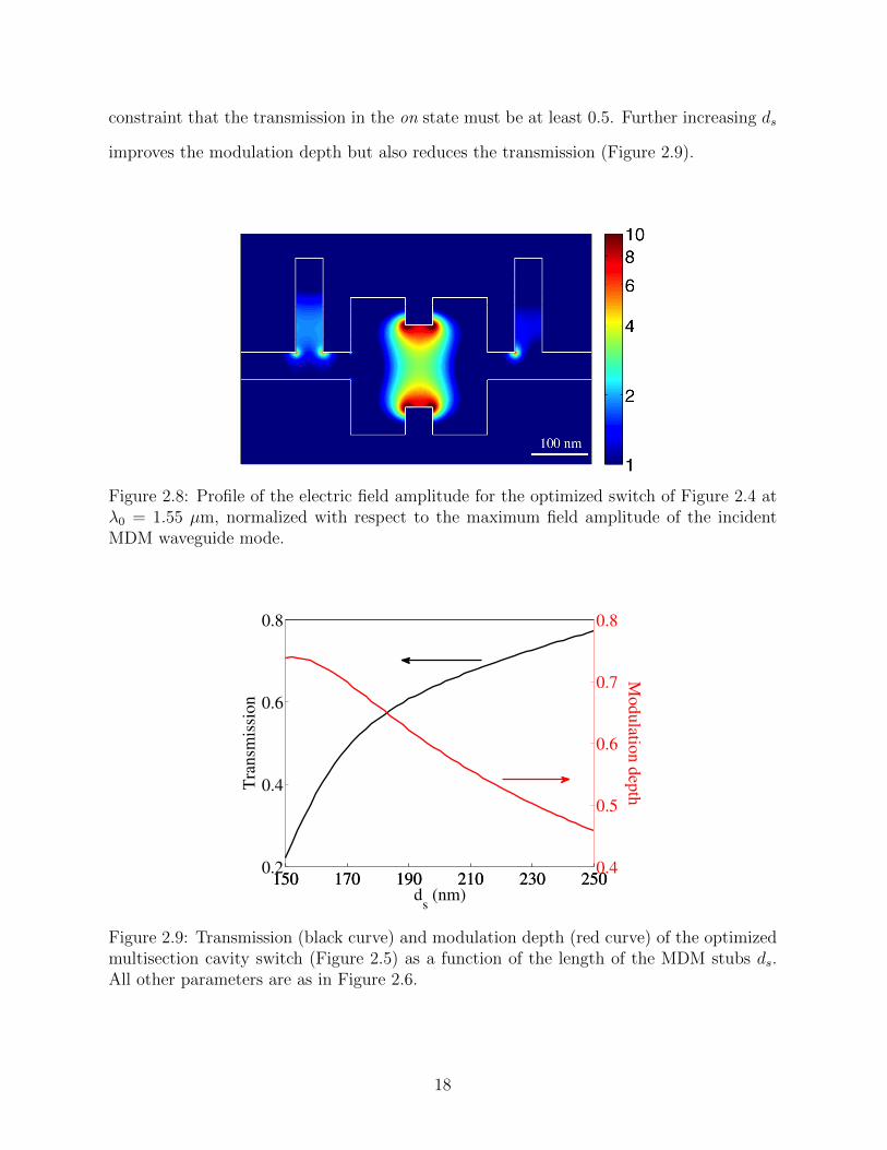
of electric field amplitude for the optimized switch is given in Figure 2.8. The concentra-
tion of electric field is around the tips of the middle section of the cavity filled with active
material. The enhanced field energy in the cavity increases the interaction of light with
matter, and the absorption in the off state is therefore enhanced.
Again the transmission and modulation depth for the switch if the metal is lossless
are also obtained and shown in Figures 2.6 and 2.7, respectively (blue dashed lines). It
can be seen that in the absence of loss in the metal perfect matching leads to complete
transmission at the 1.55 µm wavelength at which the structure was optimized.
The two stubs before and after the cavity can be considered as the mirrors for the
structure to enhance the interaction of light and matter. As it can be seen in Figure 2.9
there is a trade off between transmission and modulation depth when the stub length ds
is varying. The optimized length of the stubs obtained by the optimization algorithm is
ds = 172 nm. As can be seen in Figure 2.9, the choice of this parameter is dictated by the
16

1300 1400 1500 1600 1700 18000
0.2
0.4
0.6
0.8
1
Wavelength (nm)
Tra
nsm
issi
on
Lossless
Lossy
Figure 2.6: Transmission spectra T (κ = 0) for the optimized multisection cavity switch ofFigure 2.4 in the on state (solid line). Also shown are the transmission spectra if the metalis lossless (dashed line). Results are shown for w = 50 nm, ds = 172 nm, G = 50 nm,d1 = 250 nm, d2 = 250 nm, d3 = 150 nm, L = 50 nm.
1300 1400 1500 1600 1700 18000
0.2
0.4
0.6
0.8
1
Wavelength (nm)
Modula
tion d
epth
Lossless
Lossy
Figure 2.7: Modulation depth as a function of wavelength for the optimized switch of Figure2.4 (solid line). Also shown is the modulation depth if the metal is lossless (dashed line).All other parameters are as in Figure 2.6.
17
constraint that the transmission in the on state must be at least 0.5. Further increasing ds
improves the modulation depth but also reduces the transmission (Figure 2.9).
Figure 2.8: Profile of the electric field amplitude for the optimized switch of Figure 2.4 atλ0 = 1.55 µm, normalized with respect to the maximum field amplitude of the incidentMDM waveguide mode.
150 170 190 210 230 2500.2
0.4
0.6
0.8
Tra
nsm
issi
on
ds (nm)
150 170 190 210 230 2500.4
0.5
0.6
0.7
0.8
Mo
du
lation
dep
th
Figure 2.9: Transmission (black curve) and modulation depth (red curve) of the optimizedmultisection cavity switch (Figure 2.5) as a function of the length of the MDM stubs ds.All other parameters are as in Figure 2.6.
18

In addition, the width of the middle section d3 is a tuning parameter of the resonator.
More specifically, by changing d3 one can tune the resonant wavelength of the cavity (Figure
2.10). Figures 2.11 and 2.12 show that the maximum transmission and maximum modula-
tion depth of the switch are both achieved when the width of the middle section is d3 = 150
nm. This is due to the fact that when d3 = 150 nm, the resonant wavelength of the cavity
coincides with the operating wavelength (Figure 2.9). When the structure is on resonance,
the sensitivity of the transmission to the imaginary part of the dielectric constant of the
active material εri , T−1 ∂T
∂εriand therefore the modulation depth are maximized (Figure
2.13).
100 150 200 2501200
1400
1600
1800
d3 (nm)
Res
on
ant
Wav
elen
gth
(n
m)
Figure 2.10: Resonant wavelength of the multisection cavity as a function of the width ofthe middle section d3. All other parameters are as in the optimized structure of Figure 2.6.
Based on transmission line theory, the multisection cavity switch is equivalent to mul-
tiple transmission line sections sandwiched between two short-circuited transmission line
resonators of length ds [41, 54, 55]. The transmission of the multisection cavity absorption
19

50 100 150 200 2500
0.2
0.4
0.6
d3 (nm)
Tra
nsm
issi
on
Figure 2.11: Transmission of the multisection cavity switch as a function of the width ofthe middle section d3. All other parameters are as in Figure 2.6.
50 100 150 200 2500
0.2
0.4
0.6
0.8
d3 (nm)
Modula
tion d
epth
Figure 2.12: Modulation depth of the multisection cavity switch as a function of the widthof the middle section d3. All other parameters are as in Figure 2.6.
20

50 100 150 200 2500
2
4
6
8
d3 (nm)
No
rmal
ized
Sen
siti
vit
y
Figure 2.13: Normalized sensitivity of the transmission of the multisection cavity switchto the imaginary part of the dielectric constant of the active material εri , T
−1 ∂T∂εri
, as a
function of the width of the middle section d3.
switch can also be investigated by using a transfer matrix model. The structure of Figure
2.4 can be considered as a combination of five cascade sections: the left stub, the left gap,
the cavity, the right gap and the right stub. The complex magnetic field reflection and
transmission coefficients for the stubs (rs and ts) and cavity (rc and tc) can be extracted
from the fields obtained by FDFD (Figures 2.14 and 2.15). Because of the symmetry of the
structure these coefficients are the same for the left and right stubs. The power transmission
of the switch can then be calculated as (Appendix A):
T =
∣∣∣∣ t2stce−2γG
1− 2rsrce−2γG + (r2sr2c − r2st2c)e−4γG
∣∣∣∣2 , (2.2)
where γ is the propagation constant for the MDM waveguide with the width of w = 50
nm and G is the length of the gap between the stubs and the cavity. The transmission
21

calculated using the transfer matrix model is in excellent agreement with the one obtained
by FDFD (Figure 2.16).
Comparing Eq. 2.2 with the transmission for a conventional Fabry-Perot cavity, it
is obvious that the former is more complicated. In the absence of the cavity, the switch
can be considered as a conventional Fabry-Perot structure with the distance between the
Figure 2.14: Schematic defining the reflection coefficient rs, and transmission coefficient tswhen the fundamental TM mode of the MDM waveguide is incident at a single stub of theproposed absorption switch.
Figure 2.15: Schematic defining the reflection coefficient rc, and transmission coefficienttc when the fundamental TM mode of the MDM waveguide is incident at a cavity of theproposed absorption switch.
22

100 120 140 160 180 200 220 2400
0.1
0.2
0.3
0.4
0.5
d3
Tra
nsm
issi
on
FDFD
Model
Figure 2.16: Transmission as a function of the width of the middle section d3 for thestructure of Figure 2.4, calculated using FDFD (red solid line) and scattering matrix theory(blue dots) at λ0 = 1550 nm.
mirrors of l = 2G. Assuming tc = 1, rc = 0 and substituting these parameters in Eq. 2.2
the well-known transmission equation for Fabry-Perot structures is obtained [56]:
T =
∣∣∣∣ t2se−γl
1− r2se−2γl
∣∣∣∣2 . (2.3)
23

Chapter 3Efficient Design of NanoplasmonicWaveguide Devices Using the SpaceMapping Algorithm
3.1 Introduction
The unique properties of surface plasmons could enable a wide range of applications for
plasmonics, including light guiding and manipulation at the nanoscale [9, 57, 11, 58, 12, 4].
The realization of active and passive nanoplasmonic devices with optimal performance for
high-density optical information processing could have profound implications for computing
and communications. In designing such nanoplasmonic devices, ideally one would like to
solve inverse problems starting from design specifications imposed on the device response.
This can be achieved by combining global optimization algorithms with electromagnetic
simulations [48, 59, 60]. Such an approach leads to an extremely powerful design technique
which can enable high performance nanoplasmonic devices. In many cases, the highly effi-
cient device designs coming out of this approach cannot be obtained with any conventional
design method based on analytical techniques [61]. However, integrated nanoplasmonic de-
vices consist of multiple components and therefore have several design parameters [62, 63].
Thus, the solution of inverse problems by combining global optimization algorithms with
electromagnetic simulations often requires simulation of hundreds to thousands of candidate
structures before a design which satisfies all the specifications is reached. In most cases,
full-wave electromagnetic simulation methods are too computationally expensive for this
purpose. Thus, alternative approaches to solve inverse design problems for nanoplasmonic
devices need to be explored.
Here, we show that the space mapping algorithm, originally developed for microwave
circuit optimization, can enable the efficient design of nanoplasmonic devices which satisfy
24

a set of desired specifications. Space mapping utilizes a physics-based coarse model to
approximate a fine model accurately describing a device. The main concept in the algo-
rithm is to find a mapping that relates the fine and coarse model design parameters. If
such a mapping is established, we can then avoid directly optimizing the computationally
expensive fine model during the design process. Instead, we perform optimization of the
computationally efficient coarse model, and then use the mapping to find the corresponding
fine model design.
More specifically, we demonstrate the use of the space mapping algorithm for the
design of metal-dielectric-metal (MDM) plasmonic waveguide devices [55]. Such devices
could be potentially important in providing an interface between conventional optics and
subwavelength electronic and optoelectronic devices [41, 54]. In our case, the fine model
is a full-wave finite-difference frequency-domain (FDFD) simulation of the device, while
the coarse model is based on transmission line theory. Through several examples, we
demonstrate that simply optimizing the transmission line model of the device is not enough
to obtain a device which satisfies all the required design specifications. On the other hand,
we show that, when the iterative space mapping algorithm is used, it converges fast to a
design which meets all the specifications. In addition, full-wave FDFD simulations of only a
few candidate structures are required before the iterative process is terminated. Use of the
space mapping algorithm therefore results in large reductions in the required computation
time when compared to any direct optimization method of the fine FDFD model.
The remainder of this chapter is organized as follows. In Section 3.2, we describe the
space mapping algorithm used in this work for the design of nanoplasmonic waveguide
devices. In Section 3.3, we present several examples of the application of the algorithm for
the design of such devices.
3.2 Algorithm
Space mapping utilizes a physics-based coarse model to approximate a fine model which
accurately describes a device [64, 65, 66]. The coarse and fine model design parameters are
25

denoted by xc and xf , respectively, while the corresponding responses are denoted by Rc
and Rf . In this work it is assumed that xc and xf have the same dimensionality. In other
words, the number of design parameters n is the same for both models. The main concept
in the space mapping algorithm is to find a mapping P that relates the fine and coarse
model parameters through
xc = P(xf ), (3.1)
such that
Rc(P(xf )) ' Rf (xf ). (3.2)
We assume that such a one-to-one mapping exists in the region of interest. If such a map-
ping is established, we can then avoid using the direct optimization of the computationally
expensive fine model to find the solution x∗f . Instead, we perform optimization of the
computationally efficient coarse model to find its optimal solution x∗c , and then use
xf ≡ P−1(x∗c) (3.3)
to find an estimate of the fine model solution x∗f .
3.2.1 Aggressive space mapping
More specifically, here we use the aggressive space mapping implementation of the
algorithm [64], which incorporates a quasi-Newton iteration. In this approach we assume
that xc is a nonlinear vector function P of xf (Eq. 3.1).
In the first step, we perform optimization of the computationally efficient coarse model
and find its optimal solution x∗c . Eq. 3.3 can be rewritten as
P(xf )− x∗c = 0. (3.4)
26

Thus, the solution of the space mapping algorithm xf can be found by solving the system
of nonlinear equations
g(xf ) = 0, (3.5)
where
g(xf ) ≡ P(xf )− x∗c . (3.6)
We can therefore use a quasi-Newton iterative method to solve this problem. Since the
Jacobian matrix corresponding to Eq. 3.5
J(xf ) =
[∂Tg(xf )
∂xf
]T(3.7)
cannot be directly calculated, we use an approximation for the Jacobian matrix based on
the Broyden formula [64, 67].
The initial point for the algorithm is the optimal solution of the coarse model x∗c
x(1)f = x∗
c . (3.8)
If x(j)f is the jth approximation to the solution of Eq. 3.5 then x
(j+1)f is found by
x(j+1)f = x
(j)f + h(j), (3.9)
where h(j) is the solution of the following linear system
B(j)h(j) = −g(j). (3.10)
In the above equation g(j) is obtained by
g(j) ≡ g(x(j)f ) = P(x
(j)f )− x∗
c , (3.11)
27

where P(x(j)f ) is calculated using the parameter extraction procedure described below, while
B(j) is obtained by the Broyden formula [67]
B(1) = I, (3.12)
B(j) = B(j−1) +g(j)h(j−1)T
h(j−1)Th(j−1). (3.13)
The iterative procedure is terminated after M iterations when the fine model response
Rf (x(M)f ) satisfies the set of desired specifications.
3.2.2 Parameter extraction
At each iteration of the space mapping algorithm we use a parameter extraction proce-
dure to obtain the mapping xc = P(xf ) which corresponds to the optimum match between
the coarse and fine model responses. More specfically, we use an optimization algorithm
in combination with the coarse model of the structure to minimize the objective function
H(xc)
minxc
H(xc), (3.14)
where
H(xc) =n∑i=1
ρk(ei(xc)). (3.15)
Here, ei is the error at frequency ωi, defined as the difference between the responses calcu-
lated with the coarse and fine models
ei(xc) ≡ Rc(xc, ωi)−Rf (xf , ωi), (3.16)
and ρk(ei) is the Huber norm [68, 69] given by
28

ρk(ei) ≡
e2i /2 , if |ei|≤ k
k|ei|−k2/2 , if |ei|> k.
(3.17)
The Huber norm is robust against large errors ei [64]. Here we use k = 0.04.
3.2.3 Application of the space mapping algorithm to design of nanoplasmonicwaveguide devices
Here, we demonstrate the use of the space mapping algorithm for the design of nanoplas-
monic waveguide devices. We assume that a set of desired specifications are imposed on the
transmission response of the device. We wish to find the design parameters of the device
so that its transmission response satisfies all the specifications. In our case, the fine model
is a full-wave finite-difference frequency-domain (FDFD) simulation of the device [70, 50].
This method allows us to directly use experimental data for the frequency-dependent di-
electric constant of metals such as silver [44], including both the real and imaginary parts,
with no approximation. Perfectly matched layer (PML) absorbing boundary conditions are
used at all boundaries of the simulation domain [45, 71]. We use a fine spatial grid size in
FDFD to ensure the convergence of the numerical results. Thus the fine FDFD model gives
essentially the exact solution of the Maxwell’s equations for the given device and therefore
accurately describes the device. The coarse model is based on transmission line theory and
will heretofore be referred to as the transmission line model of the device.
In our case the fine model design parameters are a set of geometric dimensions L =
[L1 L2 · · · Ln]T of the plasmonic device. The coarse transmission line model param-
eters have a one-to-one corespondence to the fine model parameters and are denoted as
LTL = [LTL1 LTL2 · · · LTLn]T . The fine and coarse model responses are the trans-
mission of the plasmonic device calculated with FDFD, TFDFD, and the transmission line
model, TTL, respectively.
29

3.3 Results
In this section, we present several examples of the application of the space mapping
algorithm for the design of nanoplasmonic waveguide devices.
3.3.1 MDM waveguide side-coupled to two MDM stub resonators
In the first example, the structure considered consists of a plasmonic MDM waveguide
side-coupled to two MDM stub resonators (Figure 3.1). The fundamental TM mode of
the MDM waveguide is incident from the left. This system is a plasmonic analogue of
electromagnetically-induced transparency (EIT) [72].
Figure 3.1: Schematic of a MDM plasmonic waveguide side-coupled to two MDM stubresonators.
Using such a waveguide device geometry, we wish to design a structure with a bandpass
filter response. More specifically, the design specifications imposed on the transmission
response T of the structure are:
30

T > 0.75 for 180 THz < f < 200 THz, (3.18a)
T < 0.2 for 130 THz < f < 160 THz and 240 THz < f < 270 THz, (3.18b)
where f is the frequency. The specifications are indicated in Figures 3.3 and 3.4 with solid
red lines. Here the design parameters are the lengths of the stub resonators L1 and L2,
while the width w of all waveguide sections is fixed at w = 50 nm.
Based on transmission line theory, the transmission line model of this structure consists
of two short-circuited transmission line resonators of lengths LTL1 and LTL2, propagation
constant γ, and characteristic impedance Z, which are connected in series to a transmission
line with the same propagation constant γ and characteristic impedance Z [73, 42] (Figure
3.2). The characteristic impedance is given by [41, 42]
Z =γ
jωεw, (3.19)
Figure 3.2: Schematic of the transmission line model for the structure of Figure 3.1. HereZ(ω) and γ(ω) are the characteristic impedance and complex propagation constant of thefundamental TM mode of a silver-air-silver plasmonic waveguide with width w.
31

where ω = 2πf , j =√−1, and ε is the dielectric permittivity of the dielectric region of the
MDM waveguide. Based on transmission line theory, the transmission line model response
130 160 190 220 2500
0.2
0.4
0.6
0.8
1
Frequency (THz)
Tra
nsm
issi
on
Figure 3.3: Transmission line model response TTL(L∗TL1, L
∗TL2) of the structure of Figure 3.1
for parameters L∗TL1 = 210 nm and L∗
TL2 = 384 nm obtained by optimizing the transmis-sion line model of Figure 3.2 (dashed blue line). We also show the transmission responsecalculated using FDFD, TFDFD(L1 = L∗
TL1, L2 = L∗TL2) for the same parameters (solid black
line). Results are shown for w = 50 nm. The red lines are the design specifications imposedon the transmission response of this structure.
130 160 190 220 2500
0.2
0.4
0.6
0.8
1
Frequency (THz)
Tra
nsm
issi
on
Figure 3.4: Transmission response TFDFD(L1, L2) of the structure of Figure 3.1 calculatedwith FDFD for the parameters L1 = 180 nm and L2 = 351 nm obtained by the spacemapping algorithm.
32

TTL(LTL1, LTL2) of the structure of Figure 3.1 can be calculated as (Appendix B) [74, 73]
TTL(LTL1, LTL2) =
∣∣∣∣∣1 +1
2
[tanh(γLTL1) + tanh(γLTL2)
]∣∣∣∣∣−2
. (3.20)
The transmission line model is computationally efficient with a required computation time
which is negligible compared to a full-wave FDFD simulation of the device. However, the
accuracy of this model is limited. The accuracy limitations of the transmission line model
for circuits of MDM plasmonic waveguides have been described in detail elsewhere [75].
As an example, the transmission line model introduces errors in the phase of the reflection
coefficient at the two interfaces of a side-coupled MDM stub resonator [76, 77].
We use the coarse transmission line model of the structure (without space mapping) in
combination with a genetic global optimization algorithm [78, 48] to find the stub lengths
LTL1 and LTL2 such that the transmission line model response TTL(LTL1, LTL2) satisfies the
design specifications. During the optimization process the transmission line model response
is calculated at a discrete set of frequencies in the passband (180 THz < f < 200 THz) and
stopbands (130 THz < f < 160 THz and 240 THz < f < 270 THz) for each structure.
The objective is to maximize the transmission TTL in the passband, and minimize it in the
stopbands. The optimal transmission line model stub lengths found using this approach
are L∗TL1 = 210 nm and L∗
TL2 = 384 nm. As shown in Figure 3.3, the transmission line
model response for the optimized device TTL(L∗TL1, L
∗TL2) (dashed blue line) meets all the
design specifications (Eq. 3.18).
We first investigate whether optimizing the transmission line model of the structure is
enough to obtain a device which satisfies all the design specifications. We therefore perform
a full-wave FDFD simulation of the device setting the stub lengths L1, L2 equal to the
optimal transmission line model stub lengths, and obtain the device response TFDFD(L1 =
L∗TL1, L2 = L∗
TL2). We observe that the transmission response of the device obtained with
this approach TFDFD(L1 = L∗TL1, L2 = L∗
TL2) (black solid line) is substantially different
33

from the transmission line model response TTL(L∗TL1, L
∗TL2) (dashed blue line), and does
not meet all the desired specifications (Figure 3.3). This is due to the limited accuracy
of the transmission line model which was discussed above. Thus, simply optimizing the
transmission line model of the device is not enough to obtain a device which satisfies all
the required design specifications.
To obtain such a device which will satisfy all the design specifications, we now use
the space mapping algorithm, described in Section 3.2. We found that the space mapping
algorithm converges fast to the design L1 = 180 nm and L2 = 351 nm with device response
TFDFD(L1, L2), which meets all the specifications (Figure 3.4). The initial point for the
algorithm is the optimal solution of the coarse transmission line model (Eq. 3.8)
[L(1)1 L
(1)2 ]T = [L∗
TL1 L∗TL2]
T = [210 nm 384 nm]T. (3.21)
We then follow the iterative process described in Section 3.2.1. At each step of the al-
gorithm the next approximation to the solution is found using Equations 3.9 and 3.10.
The design parameters L(j)1 , L
(j)2 found after the jth iteration of the algorithm are shown
in Table 3.1. Figure 3.3 shows the transmission response of the device TFDFD(L(j)1 , L
(j)2 )
after the jth iteration calculated with the fine FDFD model. The device response from
the initial step of the algorithm TFDFD(L(1)1 , L
(1)2 ), which as mentioned above is obtained
from the optimal solution of the coarse transmission line model, does not meet the desired
specifications. The device response obtained after the second iteration TFDFD(L(2)1 , L
(2)2 )
satisfies the specifications in almost the entire frequency range (Figure 3.4). Finally, af-
ter the third iteration the transmission response of the device TFDFD(L(3)1 , L
(3)2 ) calculated
with the fine FDFD model satisfies the specifications in the entire frequency range (Figure
3.4). Thus, in this example the space mapping algorithm results in a device which satisfies
all the design specifications after only 3 iterations (Figure 3.5). In other words, full-wave
FDFD simulations of only 3 candidate structures are required before the iterative process
34

is terminated. Use of the space mapping algorithm therefore results in large reductions in
the required computation time when compared to any direct optimization method of the
fine FDFD model.
Table 3.1: The design parameters L(j)1 , L
(j)2 found after jth iteration of the space mapping
algorithm for the structure of Figure 3.1.
j = 1 j = 2 j = 3
L(j)1 (nm) 210 182 180
L(j)2 (nm) 384 349 351
130 160 190 220 2500
0.2
0.4
0.6
0.8
1
Frequency (THz)
Tra
nsm
issi
on
1st iteration
2nd iteration
3rd iteration
Figure 3.5: Transmission response TFDFD(L(j)1 , L
(j)2 ) of the structure of Figure 3.1 calculated
with FDFD for parameters obtained after the jth iteration of the space mapping algorithm.L(j)1 , L
(j)2 for j = 1, 2, 3 are given in Table 3.1. All other parameters are as in Figure 3.3.
At each iteration of the space mapping algorithm, we use the parameter extraction
procedure described in Subsection 3.2.2 to obtain the mapping which corresponds to the
optimum match between the coarse transmission line and fine FDFD model responses. The
objective function H to be minimized during the parameter extraction (Eq. 3.15) is based
on the model responses at 15 frequency points from 130 THz to 270 THz with a step of
10 THz. In Figure 3.6 we show the device response from the initial step of the algorithm
35

TFDFD(L(1)1 , L
(1)2 ) (solid line). Using the parameter extraction procedure, we obtain the
mapping [L(1)TL1 L
(1)TL2]
T = P([L(1)1 L
(1)2 ]T ) = [238 nm 419 nm]T . In Figure 3.6 we also
show the corresponding coarse transmission line model response TTL(L(1)TL1, L
(1)TL2) (circles).
We observe that there is very good agreement between the device response TFDFD(L(1)1 , L
(1)2 )
and the transmission line model response TTL(L(1)TL1, L
(1)TL2) obtained through the parameter
extraction procedure in the entire frequency range. This demonstrates that a mapping P
that relates the fine FDFD and the coarse transmission line model parameters through
LTL = P(L) can indeed be established such that TTL(P(L)) ' TFDFD(L) in the frequency
range of interest. It is the existence of such a one-to-one mapping that enables the space
mapping algorithm to converge to a desired design after a few iterations. If a one-to-one
mapping between the fine and coarse models cannot be established, the algorithm may fail
to converge [65].
130 160 190 220 2500
0.2
0.4
0.6
0.8
1
Frequency (THz)
Tra
nsm
issi
on
Figure 3.6: Transmission response TFDFD(L(1)1 , L
(1)2 ) of the structure of Figure 3.1 calculated
with FDFD (solid line) for parameters obtained after the first iteration of the space map-
ping algorithm. We also show the coarse transmission line model response TTL(L(1)TL1, L
(1)TL2)
(circles), where L(1)TL1, L
(1)TL2 are obtained through the parameter extraction procedure de-
scribed in Subsection 3.2.2.
36

3.3.2 MDM waveguide side-coupled to two arrays of MDM stub resonators
We next consider an example in which space mapping is applied to the design of
a multicomponent nanoplasmonic device. The structure consists of a MDM plasmonic
waveguide side-coupled to two arrays of MDM stub resonators [79] (Figure 3.7). The
fundamental TM mode of the MDM waveguide is incident from the left.
Figure 3.7: Schematic of a MDM plasmonic waveguide side-coupled to two arrays of MDMstub resonators.
As in the previous example, we wish to design a structure with a bandpass filter re-
sponse. In the waveguide device geometry of Figure 3.7 the use of multiple stubs can reduce
the transmission in the stopbands. In addition, the use of two stub arrays with different
stub lengths can result in narrower bandwidth of the passband [79]. In this case, the design
specifications imposed on the transmission response T of the structure (indicated in Figures
3.9 and 3.10 with solid red lines) are:
37

T > 0.5 for 190 THz < f < 200 THz, (3.22a)
T < 0.03 for 110 THz < f < 160 THz and 230 THz < f < 290 THz. (3.22b)
Here the design parameters are the lengths of the stub resonators in the two arrays L1 and
L2, as well as the distance L3 between two adjacent stubs. The width w of all waveguide
sections is fixed at w = 50 nm. The first and second array consist of 3 and 4 stubs,
respectively.
Based on transmission line theory, the transmission line model of this structure con-
sists of a transmission line with propagation constant γ and characteristic impedance Z
loaded with two arrays of short-circuited transmission line stub resonators of lengths LTL1
and LTL2 with the same propagation constant γ and characteristic impedance Z (Figure
3.8). The distance between two adjacent transmission line stub resonators is LTL3. The
characteristic impedance Z is given by Eq. 3.19. To obtain the transmission line model re-
sponse of the structure TTL(LTL1, LTL2, LTL3), each of the MDM waveguide sections of the
multicomponent device is modeled using a 2×2 transfer matrix [80, 75]. The overall trans-
fer matrix is obtained by multiplying the transfer matrices of the individual components
(Appendix B) [75].
Figure 3.8: Schematic of the transmission line model for the structure of Figure 3.7. HereZ(ω) and γ(ω) are the characteristic impedance and complex propagation constant of thefundamental TM mode of a silver-air-silver plasmonic waveguide with width w.
38

As in the previous example, the transmission line model of this structure is compu-
tationally efficient but its accuracy is limited. We use the coarse transmission line model
of the structure (without space mapping) in combination with the genetic global opti-
mization algorithm to find the transmission line model parameters LTL1, LTL2, and LTL3
such that the transmission line model response TTL(LTL1, LTL2, LTL3) satisfies the design
specifications. The optimal transmission line model parameters found using this approach
are L∗TL1 = 183 nm, L∗
TL2 = 466 nm, and L∗TL3 = 229 nm. As shown in Figure 3.9, the
transmission line model response for the optimized device TTL(L∗TL1, L
∗TL2, L
∗TL3) (dashed
blue line) meets all the design specifications (Eq. 3.22).
130 160 190 220 250 2800
0.2
0.4
0.6
Frequency (THz)
Tra
nsm
issi
on
Figure 3.9: Transmission line model response TTL(L∗TL1, L
∗TL2, L
∗TL3) of the structure of
Figure 3.7 for parameters L∗TL1 = 183 nm, L∗
TL2 = 466 nm, and L∗TL3 = 229 nm obtained
by optimizing the transmission line model of Figure 3.8 (dashed blue line). We also show thetransmission response calculated using FDFD, TFDFD(L1 = L∗
TL1, L2 = L∗TL2, L3 = L∗
TL3)for the same parameters (solid black line). Results are shown for w = 50 nm. The red linesare the design specifications imposed on the transmission response of this structure.
39

As in the previous example, we investigate whether optimizing the transmission line
model of the structure is enough to obtain a device which satisfies all the design specifica-
tions. We therefore perform a full-wave FDFD simulation of the device setting the design
parameters L1, L2, L3 equal to the optimal transmission line model parameters, and ob-
tain the device response TFDFD(L1 = L∗TL1, L2 = L∗
TL2, L3 = L∗TL3). We observe that the
transmission response of the device obtained with this approach TFDFD(L1 = L∗TL1, L2 =
L∗TL2, L3 = L∗
TL3) (black solid line) is substantially different from the transmission line
model response TTL(L∗TL1, L
∗TL2, L
∗TL3) (dashed blue line), and does not meet all the desired
specifications (Figure 3.9). This is due to the limited accuracy of the transmission line
model which was discussed above. Thus, as in the previous example, simply optimizing
the transmission line model of the device is not enough to obtain a device which satisfies
all the required design specifications.
We therefore then use the space mapping algorithm (Section 3.2), to obtain a device
which will satisfy all the design specifications. The objective function H to be minimized
during the parameter extraction (Eq. 3.15) is based on the coarse transmission line and
fine FDFD model responses at 21 frequency points from 100 THz to 300 THz with a step
of 10 THz. The design parameters L(j)1 , L
(j)2 , L
(j)3 found after the jth iteration of the
algorithm are shown in Table 3.2. In this example the space mapping algorithm results
in the design L1 = 159 nm, L2 = 439 nm, L3 = 196 nm, which satisfies all the design
specifications (Figure 3.10), after only 3 iterations. Thus, as in the previous example, the
use of the space mapping algorithm results in large reductions in the required computation
time when compared to any direct optimization method of the fine FDFD model.
3.3.3 Two nanorods juxtaposed in parallel in a waveguide
We also consider an example where space mapping is applied to the design of a nanoplas-
monic device which includes deep subwavelength dielectric and metallic structures. Due
to their deep subwavelength dimensions, these structures are modeled as lumped circuit
40

Table 3.2: The design parameters L(j)1 , L
(j)2 , and L
(j)3 found after jth iteration of the space
mapping algorithm for the structure of Figure 3.7.
j = 1 j = 2 j = 3
L(j)1 (nm) 183 156 159
L(j)2 (nm) 466 439 439
L(j)3 (nm) 229 196 196
130 160 190 220 250 2800
0.2
0.4
0.6
Frequency (THz)
Tra
nsm
issi
on
Figure 3.10: Transmission response TFDFD(L1, L2, L3) of the structure of Figure 3.7 cal-culated with FDFD for the parameters L1 = 159 nm, L2 = 439 nm, and L3 = 196 nmobtained by the space mapping algorithm.
elements rather than as transmission lines. In this example, the plasmonic device consists
of a silicon (εr = 14.15) and a silver nanorod juxtaposed in parallel in a waveguide [81, 82]
(Figure 3.11). The parallel-plate waveguide is bounded on top and bottom by perfect elec-
tric conductors (PEC), which represent an impenetrable metal with sufficiently negative
permittivity in the frequency range of interest [82]. The nanorods are connected to a PEC
protrusion attached to the bottom of the waveguide (Figure 3.11). The fundamental TEM
mode of the parallel-plate waveguide is incident from the left.
41

Figure 3.11: Schematic of a nanoplasmonic waveguide device consisting of a silicon anda silver nanorod juxtaposed in parallel in a waveguide. The parallel-plate waveguide isbounded on top and bottom by perfect electric conductors (PEC). The nanorods are con-nected to a PEC protrusion attached to the bottom of the waveguide.
Here we wish to use the plasmonic waveguide device of Figure 3.11, which is based
on two optical lumped nanocircuit elements, to design a structure with a bandpass filter
response. More specifically, the design specifications imposed on the transmission response
T of the structure are
T > 0.36 for 330 THz < f < 360 THz, (3.23a)
T < 0.18 for 120 THz < f < 270 THz and 420 THz < f < 630 THz. (3.23b)
The specifications are indicated in Figures 3.13 and 3.14 with solid red lines. Here the
design parameters are the lengths of the silicon and silver nanorods L1 and L2, while the
width w of the waveguide and t of the nanorods are fixed at w = 50 nm and t = 10 nm,
respectively.
As mentioned above, the nanorods can be modeled as lumped circuit elements [82].
More specifically, since the dielectric constant of silicon is real and positive, the silicon
42

nanorod is modeled as a lumped capacitor with a capacitance per unit length given by [82]
C = ε0εrL1
t. (3.24)
In addition, since the real part of the dielectric constant of silver is negative in the frequency
range of interest, the silver nanorod is modeled as a lumped inductor in parallel to a lumped
resistor. Here the resistor accounts for the material losses in the silver nanorod. The
inductance and resistance per unit length are associated with the real and imaginary parts
of the dielectric constant of silver, respectively, and are given by [82]
L = − t
ω2Re(εm)L2
, (3.25)
R =t
ωIm(εm)L2
, (3.26)
where εm is the dielectric permittivity of silver. Thus, overall the silicon and silver nanorods
are equivalent to the parallel combination of a resistor, an inductor, and a capacitor. The
transmission line model of the waveguide device of Figure 3.11 therefore consists of a shunt
impedance Zt coupled in parallel to a transmission line with characteristic impedance Z0
(Figure 3.12). Here the shunt impedance is given by
Zt = (Z−1C +R−1 + Z−1
L )−1 = [jωC +R−1 + (jωL)−1]−1, (3.27)
while the characteristic impedance of the PEC parallel-plate waveguide is [73]
Z0 =
õ0
ε0w. (3.28)
Based on transmission line theory, the transmission line model response TTL(LTL1, LTL2)
of the structure of Figure 3.11 can be calculated as (Appendix B) [73]
43

TTL =
∣∣∣∣ 2Zt2Zt + Z0
∣∣∣∣2 . (3.29)
As in the previous examples, we first use the coarse transmission line model of the
structure (without space mapping) in combination with the genetic global optimization
algorithm to find the nanorod lengths LTL1 and LTL2 such that the transmission line model
response TTL(LTL1, LTL2) satisfies the design specifications. The optimal transmission line
model nanorod lengths found using this approach are L∗TL1 = 20 nm and L∗
TL2 = 7 nm.
As shown in Figure 3.13, the transmission line model response for the optimized device
TTL(L∗TL1, L
∗TL2) (dashed blue line) meets all the design specifications (Eq. 3.23). As in
previous examples, we then investigate whether optimizing the transmission line model of
the structure is enough to obtain a device which satisfies all the design specifications. We
therefore perform a full-wave FDFD simulation of the device setting the nanorod lengths
L1, L2 equal to the optimal transmission line model nanorod lengths, and obtain the device
response TFDFD(L1 = L∗TL1, L2 = L∗
TL2). We observe that the transmission response of the
device obtained with this approach TFDFD(L1 = L∗TL1, L2 = L∗
TL2) (black solid line) is
different from the transmission line model response TTL(L∗TL1, L
∗TL2) (dashed blue line),
and does not meet all the desired specifications (Figure 3.13). This is due to the limited
Figure 3.12: Schematic of the transmission line model for the structure of Figure 3.11.Here Z0 is the characteristic impedance of the PEC parallel-plate waveguide. The shuntimpedance Zt consists of the parallel combination of a capacitor, a resistor, and an inductor.
44

accuracy of the transmission line model. Thus, similarly to the previous examples, simply
optimizing the transmission line model of the device is not enough to obtain a device which
satisfies all the required design specifications.
200 300 400 500 6000
0.1
0.2
0.3
0.4
0.5
0.6
Frequency (THz)
Tra
nsm
issi
on
Figure 3.13: Transmission line model response TTL(L∗TL1, L
∗TL2) of the structure of Figure
3.11 for parameters L∗TL1 = 20 nm and L∗
TL2 = 7 nm obtained by optimizing the transmis-sion line model of Figure 3.12 (dashed blue line). We also show the transmission responsecalculated using FDFD, TFDFD(L1 = L∗
TL1, L2 = L∗TL2) for the same parameters (solid
black line). Results are shown for w = 50 nm and t = 10 nm. The red lines are the designspecifications imposed on the transmission response of this structure.
We therefore use the space mapping algorithm (Section 3.2), to obtain a device which
will satisfy all the design specifications. As in the previous examples, the space mapping
algorithm converges fast to the design L1 = 20 nm and L2 = 9 nm, which meets all the
specifications (Figure 3.14). In this case, the objective function H to be minimized during
the parameter extraction (Eq. 3.15) is based on the coarse transmission line and fine FDFD
model responses at 18 frequency points from 120 THz to 630 THz with a frequency step of
30 THz. The design parameters L(j)1 and L
(j)2 found after the jth iteration of the algorithm
are shown in Table 3.3. In this case, only 2 iterations were required for the algorithm to
converge to a design satisfying all the specifications. Thus, as in the previous examples, the
45

use of the space mapping algorithm results in large reductions in the required computation
time when compared to any direct optimization method of the fine FDFD model.
200 300 400 500 6000
0.1
0.2
0.3
0.4
0.5
0.6
Frequency (THz)
Tra
nsm
issi
on
Figure 3.14: Transmission response TFDFD(L1, L2) of the structure of Figure 3.11 calculatedwith FDFD for the parameters L1 = 20 nm and L2 = 9 nm obtained by the space mappingalgorithm.
Table 3.3: The design parameters L(j)1 , L
(j)2 found after jth iteration of the space mapping
algorithm for the structure of Figure 3.11.
j = 1 j = 2
L(j)1 (nm) 20 20
L(j)2 (nm) 7 9
3.3.4 Emulation of 2D MDM plasmonic waveguide devices with 3D coaxialwaveguide devices
Looking at the transmission spectra of a 3D plasmonic coaxial waveguide [83] side-
coupled to two open-circuited coaxial stub resonators (Figure 3.15) one can see that they
are very similar to that of a 2D MDM waveguide side-coupled to two MDM stub resonators
[84]. Here we show that, by applying the space mapping algorithm and with proper choice
of their design parameters, a 3D plasmonic coaxial waveguide-cavity device and a 2D MDM
waveguide-cavity device can have nearly identical transmission spectra. Figure 3.16 shows
46

the top view schematic at z = 0 of the structure and Figure 3.17 shows the cross section
of the coaxial waveguide used in the 3D device.
Figure 3.15: Schematic of a plasmonic coaxial waveguide side-coupled to two open-circuitcoaxial stub resonators. The propagation direction of light is indicated by red arrows.
Figure 3.16: Top view schematic at z = 0 (Figure 3.17) of a plasmonic coaxial waveguideside-coupled to two open-circuit coaxial stub resonators.
47

Figure 3.17: Cross section of the reference plasmonic coaxial waveguide.
More specifically, we consider a 2D silver-air-silver MDM plasmonic waveguide side-
coupled to two short-circuited MDM stub resonators (Figure 3.18). The transmission
spectra of the 3D plasmonic coaxial waveguide side-coupled to two open-circuited coaxial
stub resonators are shown in Figure 3.19 (solid line). We use the space mapping algorithm
to find the optimum match between the responses of the 2D (Figure 3.18) and 3D (Figure
3.15) plasmonic waveguide devices.
Figure 3.18: Schematic of a two-dimensional silver-air-silver MDM plasmonic waveguideside-coupled to two short-circuited MDM stub resonators.
48

Thus, the design specifications in this case are the transmission spectra of the 3D
plasmonic coaxial waveguide side-coupled to two open-circuited coaxial stub resonators,
and the design parameters are the stub lengths L1, L2. The width w of all waveguide
sections is fixed at w = 50 nm. The objective function H to be minimized during the
parameter extraction (Eq. 3.15) is based on the coarse transmission line and fine FDFD
model responses at 13 frequency points from 100 THz to 340 THz with a step of 20 THz. In
this example, only 3 iterations are required for the algorithm to satisfy the specifications.
Using this approach, we find that, when the stub lengths L1 and L2 of the 2D MDM de-
vice (Figure 3.18) are optimized, its transmission spectra almost exactly match the spectra
of the 3D device (Figure 3.19).
100 150 200 250 3000
0.2
0.4
0.6
0.8
1
Frequency (THz)
Tra
nsm
issi
on
Figure 3.19: Transmission spectra for the two-dimensional structure of Figure 3.18 calcu-lated using FDFD for w = 50 nm, L1 = 354 nm, and L2 = 154 nm (solid green line).Also shown are the transmission spectra for the three-dimensional structure of Figure 3.16calculated using FDFD for L1 = 160 nm and L2 = 42 nm (red dots).
While here we found a 2D structure which matches the response of a 3D structure,
the opposite process is also possible: we can use the space mapping algorithm to find a
49

3D structure with nearly identical response to that of a 2D structure. This is particularly
useful for the practical implementation of plasmonic waveguide-cavity devices. Most of
the theoretical investigations of plasmonic waveguide-cavity systems have focused on 2D
structures [42, 72, 74, 85, 86, 87, 88, 89, 90, 91, 92, 93, 94]. This is due to the smaller
computational cost of full-wave electromagnetic simulations in 2D compared to 3D, as
well as the simplicity of visualizing and understanding the underlying optical physics in 2D
[95]. However, practical realization of these waveguide-cavity systems requires the use of 3D
structures. Since with proper choice of design parameters 3D plasmonic coaxial waveguide-
cavity devices can have nearly identical transmission spectra to that of 2D MDM devices,
the 2D designs can be translated into 3D designs suitable for experimental realization.
Thus, 3D plasmonic coaxial waveguides offer a platform for practical implementation of 2D
MDM devices.
50

Chapter 4Sensitivity Analysis of ActiveNanophotonic Devices
4.1 Introduction
It has been shown that plasmonic devices enable manipulating and guiding light at deep
subwavelength scales using surface plasmons propagating at metal-dielectric interfaces. As
was discussed in Chapter 1, in addition to developing passive nanooptical devices, it is also
important to introduce devices which can actively control the flow of light at the nanoscale.
In fact, active control of optical signals in plasmonic devices is one of the main challenges
when designing efficient active devices such as switches, modulators or sensors. Recently,
substantial progress in the development of active plasmonic devices has been achieved.
There are several different approaches to optimize photonic structures and devices
[96]. If an optimization method uses local gradients, the adjoint method may be used to
efficiently compute these [97]. In order to design an active optical device, it is important
to calculate the effect of a small change of the refractive index of the active material on
the device response function. For example, the device response function can be one of the
eigenmodes of the system or the power transmission coefficient.
The adjoint variable method is one of the most efficient methods to calculate the
sensitivity of a response function with respect to any design parameter. In the optimization
process of a photonic device, in order to find the gradient of the response function with
respect to all design parameters, it is usually required to perform an additional number of
simulations, which is equal to the number of parameters. Fortunately, if the target function
is specified in advance, using the adjoint variable method, one can calculate the gradient
with respect to all device parameters with only one additional device simulation.
51

In general, the adjoint variable method utilizes the main simulation of the device along
with an extra one called the adjoint simulation whose excitation is based on the response
function. In a way, the adjoint solution enables us to calculate the effect of any parameter
variation on the device response function, and using this solution one can avoid solving the
main problem for each parameter variation. Interestingly, in some specific cases it is possible
to reduce the required number of simulations from two to one by finding analytically a
mapping between the solutions of the main and adjoint problems. This approach is called
self adjoint variable method in which the sensitivities of the response function with respect
to all design parameters are calculated without any extra simulations.
Although the adjoint variable method is not widely used in nanophotonic design, it
is a well-known approach which has been implemented for various applications since the
1970s. For instance, it has been used in control theory as early as 1971 [98], and also in
error estimation or propagation [99, 100], and fluid mechanics [101]. It was also utilized in
performing aerodynamic shape optimizations [102, 103, 104, 105, 106], and structural design
[107]. Electrical engineers have used it in the microwave regime first [108, 109, 110, 111],
and recently the approach has been used in the optical wavelength range by a few groups
[50, 112, 113, 114, 115, 116].
Here we present an analytical adjoint sensitivity method for the power transmission
coefficient of nano-optical devices which is directly derived from Maxwell’s equations and
does not assume any discretization. Moreover, by deriving a formula which relates the
fields of the adjoint problem and forward problem in symmetric devices, we could obtain
the sensitivities with only one numerical simulation. In the second part of this chapter, we
apply the derived formula to calculate the sensitivity of the power transmission coefficient
with respect to the real and imaginary parts of the dielectric permittivity of the active
material for two-dimensional and three-dimensional plasmonic devices. We also compare
the results with the ones obtained by directly calculating the sensitivity. We find that there
52

is excellent agreement between the results obtained with the two methods. This is evidence
that the derived formula gives accurate results for the plasmonic devices of interest.
4.2 Derivation of the analytical sensitivity formula
Figure 4.1: An arbitrary two-port device.
We consider a lossless two-port structure, and assume that a single (fundamental)
mode is propagating in each port (Figure 4.1). The real modal vectors of electric ei and
magnetic hi fields in the ith port, which are biorthonormal [73, 117], can be normalized
over the terminal plane of the port as:
¨Si
(ei × hi) · ds = 1; i = 1, 2, (4.1)
where:
ds = ands, (4.2)
and an is the port unit normal vector, which in our case coincides with the direction of
propagation. Si is the cross section of the ith port. Ei is the electric field resulting from
exciting the ith port, and Einci is the incident field at the ith port. Ainc
i is defined as the
modal magnitude of the incident wave at the ith port, and Aki is defined as the modal
magnitude of the wave at port k, when the structure is excited from the ith port
Ainci ≡
¨Si
(Einci × hi
)· ds; i = 1, 2, (4.3)
53

Aki ≡¨Sk
(Ei × hk) · ds; i, k = 1, 2. (4.4)
The power transmission coefficient T at port 2 when the system is excited from port 1 is
defined as:
T ≡ Pout
Pin
=P2
P0
, (4.5)
in which Pin = P0 represents the incident power at the input (port 1) and Pout = P2
represents the output power at port 2. The output power can be written as:
Pout =
¨S2
1
2Re (E1 ×H∗
1) · ds =
¨S2
1
2Re [(A21e2)× (A21h2)
∗] · ds. (4.6)
Since the modal fields ei and hi are real, the power transmission coefficient (Eq. 4.5) can
be rewritten as:
T =Pout
Pin
=
˜S2
12|A21|2(e2 × h2) · ds
P0
=
˜S2
12
(A21A∗21) (e2 × h2) · dsP0
. (4.7)
The sensitivity of the transmission T with respect to an optimizable parameter p is the
derivative of T with respect to that parameter and can be calculated as:
dT
dp=
1
2P0
{¨S2
[(dA21
dpe2
)× (A∗
21h2)
]· ds +
¨S2
[(A21e2)×
(dA∗
21
dph2
)]· ds}
=1
2P0
¨S2
[(dA21
dpe2
)× (A∗
21h2)
]· ds +
1
2P0
{¨S2
[(dA21
dpe2
)× (A∗
21h2)
]· ds}∗
=1
P0
Re
{¨S2
[(dA21
dpe2
)× (A∗
21h2)
]· ds}
=1
P0
Re (C) , (4.8)
54

where C is defined as:
C ≡¨S2
[(dA21
dpe2
)× (A∗
21h2)
]· ds =
¨S2
{[(A∗
21h2)× an] ·(dA21
dpe2
)}ds
=
¨S2
{[(A∗
21h2)× an] · dE1
dp
}ds. (4.9)
The source free Maxwell’s equations are:
∇×H− jωε · E = 0, (4.10)
∇× E + jωµ ·H = 0. (4.11)
The differentiation of them with respect to p gives:
∇× dH
dp− jω dε
dp· E− jωε · dE
dp= 0, (4.12)
∇× dE
dp+ jω
dµ
dp·H + jωµ · dH
dp= 0. (4.13)
We then introduce the adjoint fields which satisfy Maxwell’s equations with the medium
dielectric permittivity and magnetic permeability tensors being the transpose of those in
the original problem [118]:
∇× H− jωεT · E = 0, (4.14)
∇× E + jωµT · H = 0. (4.15)
55

The adjoint fields also satisfy the same boundary conditions as the original fields. By
mathematically manipulating Equations 4.12-4.15, we obtain the following equation [118]:
∇ ·(
E× dH
dp− dE
dp× H
)= jω
[(dµ
dp·H)· H−
(dε
dp· E)· E]. (4.16)
Integrating Eq. 4.16 over the volume of the structure VS and applying the divergence
theorem leads to:
IS ≡‹S
(E× dH
dp− dE
dp× H
)· ds = jω
˚VS
[(dµ
dp·H)· H−
(dε
dp· E)· E]dv.
(4.17)
From this point on, we assume that the medium is reciprocal and its constitutive tensors
are symmetric:
ε = εT , µ = µT . (4.18)
It can be shown that the parts of the surface integral IS (Eq. 4.17) corresponding to perfect
electric conductors (PEC), perfect magnetic conductors (PMC), and radiation/absorbing
boundaries, which can be considered as radiation or reflection-free boundary conditions
(RBC) vanish and the integral therefore reduces to the surfaces of the ports (Appendix C):
IS =∑i
¨Si
(E× dH
dp− dE
dp× H
)· ds. (4.19)
Using Maxwell’s equations for the original (Eq. 4.11) and adjoint (Eq. 4.15) fields, and
also their derivatives with respect to p we obtain:
H = − (jωµ)−1∇× E, (4.20)
56

dH
dp= − (jωµ)−1∇× dE
dp− µ−1dµ
dpH, (4.21)
H = − (jωµ)−1∇× E, (4.22)
dH
dp= − (jωµ)−1∇× dE
dp− µ−1dµ
dpH, (4.23)
and substituting them in Eq. 4.19, the surface integral IS can be rewritten as:
IS =∑i
¨Si
− (jωµ)−1
[E×
(∇× dE
dp
)− dE
dp×(∇× E
)]· ds. (4.24)
Also, it is assumed that the ports are not affected by the change of parameter p (dµdp
= 0 at
Si). The following boundary conditions apply at the ith port (see appendix D):
an × (∇× E) = Uinci − P (E) , i = 1, 2, (4.25)
an ×(∇× E
)= Uinc
i − P(E), i = 1, 2, (4.26)
in which P is a linear vector operator depending on the boundary condition. Uinci and Uinc
i
are the original and adjoint excitations at port i. Using these boundary conditions and
applying the triple product to Eq. 4.24 give us:
IS =∑i
¨Si
(jωµ)−1
{E ·[an ×
(∇× dE
dp
)]− dE
dp·[an ×
(∇× E
)]}ds
=∑i
¨Si
(jωµ)−1
{E ·[dUinc
i
dp− P
(dE
dp
)]− dE
dp·[Uinci − P
(E)]}
ds
57

=∑i
{¨Si
(jωµ)−1
[−E · P
(dE
dp
)+dE
dp· P(E)]
ds
+
¨Si
(jωµ)−1 E · dUinci
dpds−
¨Si
(jωµ)−1 dE
dp· Uinc
i ds
}. (4.27)
It can be shown that [119]:
¨Si
E · P(dE
dp
)ds =
¨Si
dE
dp· P(E)ds. (4.28)
Considering that the ports are not affected by the change of the parameter p, we have
dUinci
dp= 0. By applying this into Eq. 4.27, and using Eq. 4.28 IS simplifies to:
IS = −∑i
¨Si
dE
dp· (jωµ)−1 · Uinc
i ds. (4.29)
It is obvious that, if the adjoint source is set to be :
Uinc
1 = 0,
Uinc2 = −jωA∗
21µ · (h2 × an) ,
(4.30)
then inserting Eq. 4.30 into Eq. 4.29, and using Eq. 4.9 we obtain:
IS = C. (4.31)
Finally, using Eq. 4.17 we get:
IS = C = jω
˚VS
[(dµ
dp·H1
)· H2 −
(dε
dp· E1
)· E2
]dv, (4.32)
and the formula for the sensitivity of transmission (Eq. 4.8) can be written as:
58

dT
dp=
1
P0
Re
(jω
˚VS
[(dµ
dp·H1
)· H2 −
(dε
dp· E1
)· E2
]dv
). (4.33)
Since the modal vector h2 at the second port describes a propagating mode, it satisfies the
boundary condition (Appendix D):
an × (jωµ · h2) = P (e2) . (4.34)
Substituting Eq. 4.34 into Eq. 4.30 we obtain:
Uinc2 = A∗
21P (e2) . (4.35)
In the original simulation, if the second port is excited, we have:
Uinc2 = 2P
(Einc
2
)= 2P
(Ainc
2 e2
)= 2Ainc
2 P (e2) , (4.36)
where we used the fact that P is a linear operator. Eq. 4.36 can also be written as:
P (e2) =Uinc
2
2Ainc2
. (4.37)
Inserting Eq. 4.37 into Eq. 4.35, we get:
Uinc2 = A∗
21
1
2Ainc2
Uinc2 . (4.38)
Considering the fact that the adjoint fields satisfy the same Maxwell’s equations and the
same boundary conditions as the original fields and with the assumption of having reciprocal
media, we can calculate the fields of the adjoint problem by the forward problem fields:
E2 = A∗21
1
2Ainc2
E2. (4.39)
59
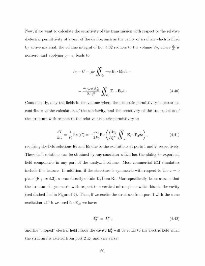
Now, if we want to calculate the sensitivity of the transmission with respect to the relative
dielectric permittivity of a part of the device, such as the cavity of a switch which is filled
by active material, the volume integral of Eq. 4.32 reduces to the volume VC , where dεdp
is
nonzero, and applying p = εr leads to:
IS = C = jω
˚VC
−ε0E1 · E2dv =
=−jωε0A∗
21
2Ainc2
˚VC
E1 · E2dv. (4.40)
Consequently, only the fields in the volume where the dielectric permittivity is perturbed
contribute to the calculation of the sensitivity, and the sensitivity of the transmission of
the structure with respect to the relative dielectric permittivity is:
dT
dεr=
1
P0
Re (C) = −ωε02P0
Re
(jA∗
21
Ainc2
˚VC
E1 · E2dv
), (4.41)
requiring the field solutions E1 and E2 due to the excitations at ports 1 and 2, respectively.
These field solutions can be obtained by any simulator which has the ability to export all
field components in any part of the analyzed volume. Most commercial EM simulators
include this feature. In addition, if the structure is symmetric with respect to the z = 0
plane (Figure 4.2), we can directly obtain E2 from E1. More specifically, let us assume that
the structure is symmetric with respect to a vertical mirror plane which bisects the cavity
(red dashed line in Figure 4.2). Then, if we excite the structure from port 1 with the same
excitation which we used for E2, we have:
Ainc2 = Ainc
1 , (4.42)
and the ”flipped” electric field inside the cavity Ef1 will be equal to the electric field when
the structure is excited from port 2 E2 and vice versa:
60

Figure 4.2: A symmetric two-port device.
E2 = Ef1 . (4.43)
More specifically, if z = 0 is the mirror plane bisecting the cavity (and the overall structure),
then the “flipped” electric field will be:
Ef1x (z) = E1x (−z) , (4.44)
Ef1y (z) = E1y (−z) , (4.45)
Ef1z (z) = −E1z (−z) . (4.46)
Therefore, the sensitivity can be obtained by just a single simulation as:
dT
dεr=
1
P0
Re (C) = −ωε02P0
Re
(jA∗
21
Ainc1
˚VC
E1 · Ef1dv
). (4.47)
If we assume that εr is a complex number, then we can find the sensitivity of the transmis-
sion with respect to the real or imaginary part of εr by substituting:
dε
dRe (εr)= ε0, (4.48)
61

dε
dIm (εr)= jε0, (4.49)
into Eq. 4.33, respectively. This leads to the following two sensitivity formulas:
dT
dRe (εr)= −ωε0
2P0
Re
(jA∗
21
Ainc1
˚VC
E1 · Ef1dv
), (4.50)
dT
dIm (εr)=ωε02P0
Re
(A∗
21
Ainc1
˚VC
E1 · Ef1dv
). (4.51)
4.3 Numerical implementation
In this section, we present some examples of the application of the proposed method
to find the sensitivity of the transmission with respect to the dielectric permittivity of the
active material of the structure. To confirm the results obtained by the proposed formula,
we have compared them with the results obtained using the direct approach. The numerical
method which we use is a full-wave finite-difference frequency-domain (FDFD) simulation
of the device [70, 50]. This method allows us to directly use experimental data for the
frequency-dependent dielectric constant of metals such as silver [44], including both the real
and imaginary parts, with no approximation. Perfectly matched layer (PML) absorbing
boundary conditions are used at all boundaries of the simulation domain [45, 71].
4.3.1 2D example
The first example which is being considered here is a 2D plasmonic switch consisting of
a multisection cavity between two resonators (two MDM stubs). The structure is symmetric
with respect to a vertical mirror plane which bisects the middle section of the cavity (Figure
4.3). The waveguide and resonators are filled with an active material with relative dielectric
permitivity of εc = εcr + jεci, which can be a complex number. For the direct approach the
62

on state of the switch corresponds to εc = 4.804. If we want to find the sensitivity with
respect to the real part of εc we will change it to εc = 4.904 in the cavity region for the on
state. If we want to find the sensitivity with respect to the imaginary part of εc, we will
change it to εc = 4.804 + i0.01 in the cavity region for the off state.
For a fixed structure with:
ds = 172 nm,
dc = 150 nm,
we have investigated the sensitivity of the transmission on the dielectric permittivity of
the active material inside the cavity using both the proposed equations (Eq. 4.50 and Eq.
4.51), as well as the Direct Approach (DA) for different wavelengths. We first consider a
lossless structure. In other words, the metal is assumed to be lossless in these simulations.
Since the dielectric permittivity is complex, the sensitivity is calculated for two different
cases. First, we assume that the dielectric permittivity of the active material for both the
on and off states is a real number (no loss in the cavity). We first use the proposed
sensitivity formula to find the sensitivity of the transmission with respect to the real part
of the relative dielectric permittivity inside the cavity:
Figure 4.3: Schematic of an absorption switch consisting of a MDM plasmonic waveguidecoupled to a resonator. The resonator is formed by a cavity comprising of multiple sectionsof varying widths sandwiched between two MDM stubs.
63

dT
dRe (εr)= −ωε0
2P0
Re
(jA∗
21
Ainc1
˚VC
E1 · Ef1dv
), (4.52)
and then we compare it with the direct approach results (Figure 4.4). In the direct ap-
proach, we directly calculate the sensitivity by approximating the derivative with a finite
difference:
Dc =dT
dRe (εc)' ∆T
∆Re (εc)=T (εc = εcr + ∆εcr + jεci)− T (εc = εcr + jεci)
∆εcr. (4.53)
1300 1400 1500 1600 1700 1800
−4
−2
0
2
4
2D Lossless
Wavelength (nm)
dT/d[R
e(ǫr)]
DA
AVM
Figure 4.4: Sensitivity of the transmission with respect to the real part of the relativedielectric permittivity inside the cavity of the structure shown in Figure 4.3 in the absenceof loss in the metal. Results are calculated using the direct approach (DA) (Eq. 4.53), andthe adjoint variable method (AVM) (Eq. 4.52).
We also find the sensitivity of the transmission with respect to the imaginary part of
the relative dielectric permittivity inside the cavity (Figure 4.5). The proposed sensitivity
formula for this case is:
64

dT
dIm (εr)=ωε02P0
Re
(A∗
21
Ainc1
˚VC
E1 · Ef1dv
). (4.54)
As before, in direct approach we directly calculate the sensitivity by approximating the
derivative with a finite difference:
Dc =dT
dIm (εc)' ∆T
∆Im (εc)=T [εc = εcr + j (εci + ∆εci)]− T (εc = εcr + jεci)
∆εci. (4.55)
1300 1400 1500 1600 1700 18000
3
6
9
12 2D Lossless
Wavelength (nm)
dT/d[Im(ǫ
r)]
DA
AVM
Figure 4.5: Sensitivity of the transmission with respect to the imaginary part of the relativedielectric permittivity inside the cavity of the structure shown in Figure 4.3 in the absenceof loss in the metal. Results are calculated using the direct approach (DA) (Eq. 4.55), andthe adjoint variable method (AVM) (Eq. 4.54).
These calculations are repeated for a lossy structure (including the material loss in the
metal in the simulations) and the results are shown in Figures 4.6 and 4.7.
The sensitivities obtained by the proposed formula are in excellent agreement with the
ones obtained by the direct approach. The small differences between the two sets of results
65

1300 1400 1500 1600 1700 1800
−1
−0.5
0
0.5
1
2D Lossy
Wavelength (nm)
dT/d[R
e(ǫr)]
DA
AVM
Figure 4.6: Sensitivity of the transmission with respect to the real part of the relativedielectric permittivity inside the cavity of the structure shown in Figure 4.3. Results arecalculated using the direct approach (DA) (Eq. 4.53), and the adjoint variable method(AVM) (Eq. 4.52).
1300 1400 1500 1600 1700 18000
0.5
1
1.5
2
2.5
3
2D Lossy
Wavelength (nm)
dT/d[Im(ǫ
r)]
DA
AVM
Figure 4.7: Sensitivity of the transmission with respect to the imaginary part of the relativedielectric permittivity inside the cavity of the structure shown in Figure 4.3. Results arecalculated using the direct approach (DA) (Eq. 4.55), and the adjoint variable method(AVM) (Eq. 4.54).
66

can be attributed to errors in the numerical integration. We observe that at λ = 1550
nm, which is the resonance wavelength of the considered structure, the sensitivity of the
transmission with respect to the real part of the relative dielectric permittivity is almost
zero. This will be investigated in more detail below.
In addition, the sensitivity of the transmission with respect to the real and imaginary
parts of the relative dielectric permittivity, when the width of the middle section of the
cavity dc is varied for a fixed wavelength λ = 1550 nm, are calculated and shown in Figures
4.8 and 4.9. As before, we observe excellent agreement with the ones obtained by the direct
approach.
100 120 140 160 180 200
−1
−0.5
0
0.5
1
2D Lossy
dc (nm)
dT/d[R
e(ǫr)]
DA
AVM
Figure 4.8: Sensitivity of the transmission with respect to the real part of the relativedielectric permittivity inside the cavity of the structure shown in Figure 4.3. Results arecalculated using the direct approach (DA) (Eq. 4.53), and the adjoint variable method(AVM) (Eq. 4.52).
67

100 120 140 160 180 2000
0.5
1
1.5
2
2.5
3
2D Lossy
dc (nm)
dT/d[Im(ǫ
r)]
DA
AVM
Figure 4.9: Sensitivity of the transmission with respect to the imaginary part of the relativedielectric permittivity inside the cavity of the structure shown in Figure 4.3. Results arecalculated using the direct approach (DA) (Eq. 4.55), and the adjoint variable method(AVM) (Eq. 4.54).
4.3.2 Sensitivity at resonance
The two-port device shown in Figure 4.10 is assumed to be lossless and symmetric.
The propagation direction is z and the lines at z = z1 and z = z4 correspond to the input
and output ports respectively. We then have:
arg[Einc
1 (x, y, z = z1)]
= arg[Einc
1 (x, y, z = z2)]
+ βl, (4.56)
arg [E1 (x, y, z = z4)] = arg [E1 (x, y, z = z3)]− βl, (4.57)
where β is the propagation constant of the propagating mode in the input and output
waveguides, and l is the distance between the input port z = z1 and the beginning of the
68

Figure 4.10: A symmetric two-port device. The blue curve shows the changes of the phaseof Ex inside the cavity of Figure 4.3.
structure z = z2, which is equal to the distance between the end of the structure z = z3 and
the output port z = z4, because of the symmetry of the device. The proposed formula for
the sensitivity with respect to the real part of the dielectric permittivity inside the cavity
is:
dT
dRe (εr)= −ωε0
2P0
Re
(jA∗
21
Ainc1
˚VC
E1 · Ef1dv
). (4.58)
The phase of the term inside the real function can be written as the summation of three
phases:
arg
(jA∗
21
Ainc1
˚VC
E1 · Ef1dv
)= arg (j) + arg
(jA∗
21
Ainc1
)+ arg
(˚VS
E1 · Ef1dv
)
= arg (j) + arg
[jE∗
x1 (x, y, z = z4)
Eincx1 (x, y, z = z1)
]+ arg
(˚VS
E1 · Ef1dv
). (4.59)
The second term can be written as:
arg
[E∗x1 (x, y, z = z4)
Eincx1 (x, y, z = z1)
]= − arg [Ex1 (x, y, z = z4)]− arg
[Eincx1 (x, y, z = z1)
]. (4.60)
69

Using Eq. 4.56 and Eq. 4.57 and the fact that at resonance there is almost no reflection
we have:
arg
[E∗x1 (x, y, z = z4)
Eincx1 (x, y, z = z1)
]= − arg [Ex1 (x, y, z = z3)]− arg [Ex1 (x, y, z = z2)] . (4.61)
Before calculating the phase of the integral (third term), for the structure of Figure 4.3 we
show the phase of electric field components Ex and Ez on resonance at three different lines
x = x1 = 125 nm, x = x2 = 175 nm, and x = x3 = 225 nm inside the cavity where the
integral is being calculated (Figure 4.11). Also on each line we show the phases of EzEfz
and ExEfx in Figures 4.14, 4.18, 4.22, and Figures 4.15, 4.19, 4.23, respectively.
Figure 4.11: Profile of the electric field amplitude inside the cavity of the proposed switchof Figure 4.3 at the resonance wavelength of λ0 = 1.55 µm.
70
−100 −50 0 50 100
4
6
8
10
x = x1
z (nm)
arg (
Ez)
Figure 4.12: Phase of Ez inside the cavity at x = x1 (Figure 4.11).
−100 −50 0 50 100
−6
−4
−2
0
x = x1
z (nm)
arg (
Ex)
Figure 4.13: Phase of Ex inside the cavity at x = x1 (Figure 4.11).
71

−100 −50 0 50 100
−3
−2
−1
0
x = x1
z (nm)
arg (
Ez E
zf )
Figure 4.14: Phase of EzEfz inside the cavity at x = x1 (Figure 4.11). The dashed red line
is showing arg [Ex1 (z = z3)] + arg [Ex1 (z = z2)].
−100 −50 0 50 100
−2
0
2
4
x = x1
z (nm)
arg (
Ex E
xf)
Figure 4.15: Phase of ExEfx inside the cavity at x = x1 (Figure 4.11). The dashed red line
is showing arg [Ex1 (z = z3)] + arg [Ex1 (z = z2)].
72

−100 −50 0 50 100−1
0
1
2
3
x = x2
z (nm)
arg (
Ez)
Figure 4.16: Phase of Ez inside the cavity at x = x2 (Figure 4.11).
−100 −50 0 50 1002
2.2
2.4
2.6
2.8
3
x = x2
z (nm)
arg (
Ex)
Figure 4.17: Phase of Ex inside the cavity at x = x2 (Figure 4.11).
73

−100 −50 0 50 100
−3
−2
−1
0
x = x2
z (nm)
arg (
Ez E
zf )
Figure 4.18: Phase of EzEfz inside the cavity at x = x2 (Figure 4.11). The dashed red line
is showing arg [Ex1 (z = z3)] + arg [Ex1 (z = z2)].
−100 −50 0 50 100
−2
0
2
4
x = x2
z (nm)
arg (
Ex E
xf)
Figure 4.19: Phase of ExEfx inside the cavity at x = x2 (Figure 4.11). The dashed red line
is showing arg [Ex1 (z = z3)] + arg [Ex1 (z = z2)].
74

−100 −50 0 50 100−1
0
1
2
3
x = x3
z (nm)
arg (
Ez)
Figure 4.20: Phase of Ez inside the cavity at x = x3 (Figure 4.11).
−100 −50 0 50 1002
4
6
8
10
x = x3
z (nm)
arg (
Ex)
Figure 4.21: Phase of Ex inside the cavity at x = x3 (Figure 4.11).
75

−100 −50 0 50 100
−3
−2
−1
0
x = x3
z (nm)
arg (
Ez E
zf )
Figure 4.22: Phase of EzEfz inside the cavity at x = x3 (Figure 4.11). The dashed red line
is showing arg [Ex1 (z = z3)] + arg [Ex1 (z = z2)].
−100 −50 0 50 100
−2
0
2
4
x = x3
z (nm)
arg (
Ex E
xf)
Figure 4.23: Phase of ExEfx inside the cavity at x = x3 (Figure 4.11). The dashed red line
is showing arg [Ex1 (z = z3)] + arg [Ex1 (z = z2)].
76

We observe that, because of the symmetry of the structure, the changes of phase of the
electric field components are almost the same as we move away from each side of the cavity
towards the middle of it. This leads to a constant phase for the product of the electric field
and its “flipped” field. This constant φ0 is equal to:
φ0 = 2 arg [Ex1 (z = 0)] . (4.62)
Thus, the phase of the third term of Eq. 4.59, which is the integral of ExEfx and EzE
fz
over the cavity, would be:
arg
(˚VS
E1 · Ef1dv
)≈ 2 arg [Ex1 (z = 0)] . (4.63)
In Figures 4.14, 4.15, 4.18, 4.19, 4.22, and 4.23 the dashed red line is showing {arg [Ex1 (z = z3)]+
arg [Ex1 (z = z2)]}. Also because of the symmetry we have:
arg (Ex1 (x, y, z = z3)) + arg (Ex1 (x, y, z = z2)) = 2 arg [Ex1 (z = 0)] . (4.64)
Thus, from Eq. 4.61 and Eq. 4.63 we can conclude that:
arg
(A∗
21
Ainc1
)≈ − arg
(˚VS
E1 · Ef1dv
). (4.65)
At the end what remains as the phase of the argument of the real function in the sensitivity
formula is only π/2:
arg
(jA∗
21
Ainc1
˚VC
E1 · Ef1dv
)≈ arg (j) = π/2, (4.66)
meaning the whole argument is an imaginary number, so the real part of it would be zero,
and correspondingly the sensitivity of the transmission with respect to the real part of the
dielectric permittivity inside the cavity would be zero on resonance.
77

4.3.3 3D example
The next example which is being considered is a Fabry-Perot absorption switch based
on a coaxial plasmonic waveguide (Figure 4.24). Figure 4.25 shows the top view schematic
at z = 0 of the structure and Figure 4.26 shows the cross section of the proposed coaxial
waveguide used for the switch.
Two stub resonators are used as the mirrors at the two sides of the cavity. The metal
used is silver, and the space between the metallic parts is filled with silica. The structures
are placed on top of a silicon substrate. The waveguide and resonators are filled with an
active material with refractive index n = 1.5. If the inner and outer metals at the end of
the stubs are connected (Figures 4.27 and 4.28), the stub is short-circuited. Otherwise, it
is open-circuited (Figures 4.29 and 4.30).
Figure 4.24: Schematic of a Fabry-Perot absorption switch based on coaxial plasmonicwaveguide.
78

Figure 4.25: Top view schematic at z = 0 of a Fabry-Perot absorption switch based oncoaxial plasmonic waveguide.
Figure 4.26: Cross section of the reference plasmonic coaxial waveguide.
Figure 4.27: Schematic of a plasmonic coaxial waveguide side-coupled to a short-circuitcoaxial stub resonator. The propagation direction of light is indicated by red arrows.
79

Figure 4.28: Top view schematic at z = 0 of a plasmonic coaxial waveguide side-coupledto a short-circuit coaxial stub resonator.
Figure 4.29: Schematic of a plasmonic coaxial waveguide side-coupled to an open-circuitcoaxial stub resonator. The propagation direction of light is indicated by red arrows.
Figure 4.30: Top view schematic at z = 0 of a plasmonic coaxial waveguide side-coupledto an open-circuit coaxial stub resonator.
80

As we know, for a Fabry-Perot absorption switch most interaction between light and
matter occurs when the two stubs are close to their resonance and act as mirrors. To find
the approximate length for the stubs, we have first simulated a coaxial plasmonic waveguide
coupled to a stub resonator using FD3D. Simulation was done twice for both short-circuited
stubs (Figure 4.31) and open-circuited stubs (Figure 4.32).
100 150 200 250 300 350 4000
0.2
0.4
0.6
0.8
1 Short Circuit
Stub Length (nm)
Tra
nsm
issi
on
Figure 4.31: Transmission of a single short-circuit coaxial stub resonator as a function ofthe stub length Ls at λ0 = 1550 nm. The other geometrical parameters of the structureare as shown in Figure 4.26.
100 150 200 250 300 350 4000
0.2
0.4
0.6
0.8
1 Open Circuit
Stub Length (nm)
Tra
nsm
issi
on
Figure 4.32: Transmission of a single open-circuit coaxial stub resonator as a function ofthe stub length Ls at λ0 = 1550 nm. The other geometrical parameters of the structureare as shown in Figure 4.26.
81

As we expected the first resonant length is smaller for the open-circuit stub [84]. Thus
in our proposed Fabry-Perot absorption switch two open-circuited stub resonators are used
as mirrors at the two sides of the cavity. The waveguide and resonators are filled with an
active material with refractive index n = 1.5. The refractive index of the cavity, between
the two mirrors (stub resonators), is changed to n = 1.5 + i0.05 for the off state. The
Modulation Depth is also calculated as before:
MD =T (on)− T (off )
T (on). (4.67)
Varying Ls and Lc we have found the transmission for both on state (Figure 4.33) and
off state (Figure 4.34) and also modulation depth (Figure 4.35):
40 120 200 280 360 44010
50
90
130
170
Transmission (ON)
Lc (nm)
Ls (
nm
)
0.2
0.4
0.6
0.8
Figure 4.33: Transmission intensities of on state of the proposed Fabry-Perot absorptionswitch with two open-circuit stub resonators as functions of stub length Ls and the lengthof the cavity Lc at λ0 = 1550 nm.
82

40 120 200 280 360 44010
50
90
130
170
Transmission (OFF)
Lc (nm)
Ls (
nm
)
0.2
0.4
0.6
0.8
Figure 4.34: Transmission intensities of off state of the proposed Fabry-Perot absorptionswitch with two open-circuit stub resonators as functions of stub length Ls and the lengthof the cavity Lc at λ0 = 1550 nm.
40 120 200 280 360 44010
50
90
130
170
Modulation depth
Lc (nm)
Ls (
nm
)
0
0.2
0.4
0.6
Figure 4.35: Modulation depth of the proposed Fabry-Perot absorption switch with twoopen-circuit stub resonators as functions of stub length Ls and the length of the cavity Lcat λ0 = 1550 nm.
83

Considering transmission in the on state of more than 50% the maximum modulation depth
MD is found for:
Ls = 150 nm,
Lc = 380 nm,
to be:
MD = 0.44.
The transmission spectra for both on and off states for the optimized switch are shown in
Figures 4.36 and 4.37, while the modulation depth is shown in Figure 4.38 (solid lines). Also
shown are the transmission and modulation depth spectra if the metal is lossless (dashed
lines).
1400 1600 1800 20000
0.2
0.4
0.6
0.8
1
Wavelength (nm)
Tra
nsm
issi
on (
ON
)
Lossless
Lossy
Figure 4.36: Transmission spectra T for the optimized proposed Fabry-Perot absorptionswitch of Figure 4.24 in the on state (solid line). Also shown are the transmission spectraif the metal is lossless (dashed line). Results are shown for Ls = 150 nm, Lc = 380 nm.
84

1400 1600 1800 20000
0.2
0.4
0.6
0.8
1
Wavelength (nm)
Tra
nsm
issi
on (
OF
F)
Lossless
Lossy
Figure 4.37: Transmission spectra T for the optimized proposed Fabry-Perot absorptionswitch of Figure 4.24 in the off state (solid line). Also shown are the transmission spectraif the metal is lossless (dashed line). Results are shown for Ls = 150 nm, Lc = 380 nm.
1400 1600 1800 20000
0.1
0.2
0.3
0.4
0.5
0.6
Wavelength (nm)
Modula
tion d
epth
Lossless
Lossy
Figure 4.38: Modulation depth spectra MD for the optimized proposed Fabry-Perot ab-sorption switch of Figure 4.24 (solid line).Also shown are the modulation depth spectra ifthe metal is lossless (dashed line). Results are shown for Ls = 150 nm, Lc = 380 nm.
85

The dominant electric and magnetic fields of the selected structure are shown in Figures
4.39 and 4.40, respectively.
Figure 4.39: Amplitude of Ey of the optimized structure of Figure 4.24 (Ls = 150 nm,Lc = 380 nm) at z = 0 and λ = 1550 nm.
Figure 4.40: Amplitude of Hz of the optimized structure of Figure 4.24 (Ls = 150 nm,Lc = 380 nm) at z = 0 and λ = 1550 nm.
As we mentioned before the modulation depth of the absorption switches is associated
with the sensitivity of their transmission to the imaginary part of the dielectric constant of
the active material, which is in turn directly related to the electric field energy in the cavity
86
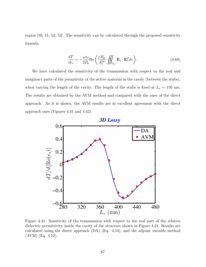
region [50, 51, 52, 53]. The sensitivity can be calculated through the proposed sensitivity
formula:
dT
dεr= −ωε0
2P0
Re
(jA∗
21
Ainc1
˚VC
E1 · Ef1dv
). (4.68)
We have calculated the sensitivity of the transmission with respect to the real and
imaginary parts of the permitivity of the active material in the cavity (between the stubs),
when varying the length of the cavity. The length of the stubs is fixed at Ls = 150 nm.
The results are obtained by the AVM method and compared with the ones of the direct
approach. As it is shown, the AVM results are in excellent agreement with the direct
approach ones (Figures 4.41 and 4.42).
280 320 360 400 440 480−0.6
−0.4
−0.2
0
0.2
0.4
0.6 3D Lossy
Lc (nm)
dT/d[R
e(ǫr)]
DA
AVM
Figure 4.41: Sensitivity of the transmission with respect to the real part of the relativedielectric permittivity inside the cavity of the structure shown in Figure 4.24. Results arecalculated using the direct approach (DA) (Eq. 4.53), and the adjoint variable method(AVM) (Eq. 4.52).
87

280 320 360 400 440 4800
0.4
0.8
1.2
1.6
3D Lossy
Lc (nm)
dT/d[Im(ǫ
r)]
DA
AVM
Figure 4.42: Sensitivity of the transmission with respect to the imaginary part of the relativedielectric permittivity inside the cavity of the structure shown in Figure 4.24. Results arecalculated using the direct approach (DA) (Eq. 4.55), and the adjoint variable method(AVM) (Eq. 4.54).
88

Chapter 5Concluding Remarks andRecommended Future Work
5.1 Conclusions
We first briefly described the history of nanophotonic devices and the need to develop
compact active nanophotonic devices, besides the widely investigated passive nanoscale
devices. We then considered an absorption switch consisting of a MDM plasmonic waveg-
uide coupled to a conventional Fabry-Perot cavity. Taking advantage of the subwavelength
modal size of MDM waveguides to enhance the interaction between light and active mate-
rial inside the cavity can lead to a compact optical switch. However, the modulation depth
of such a switch when optimized is relatively low. We therefore introduced a compact
absorption switch consisting of a multisection cavity. The optimized multisection cavity
switch led to greatly enhanced modulation depth compared to the optimized Fabry-Perot
cavity switch.
We then showed that the space mapping algorithm, originally developed for microwave
circuit optimization, can enable the efficient design of nanoplasmonic devices which satisfy
a set of desired specifications. Space mapping utilizes a physics-based coarse model to
approximate a fine model accurately describing a device.
More specifically, we demonstrated the use of the space mapping algorithm for the
design of MDM plasmonic waveguide devices. A set of desired specifications are imposed
on the transmission response of the device. The goal is to find the design parameters of
the device so that its transmission response satisfies all the specifications. In our case, the
fine model was a full-wave FDFD simulation of the device, while the coarse model was
based on transmission line theory. We used the aggressive space mapping implementation
of the algorithm, which incorporates a quasi-Newton iteration. At each iteration of the
89

space mapping algorithm we used a parameter extraction procedure to obtain the mapping
which corresponds to the optimum match between the coarse and fine model responses.
The iterative procedure was terminated when the fine model response satisfied the set of
desired specifications.
We considered several examples of the application of the space mapping algorithm
for the design of nanoplasmonic waveguide devices. In the first example, we considered a
plasmonic MDM waveguide side-coupled to two MDM stub resonators. The transmission
line model of this structure consists of two short-circuited transmission line resonators,
which are connected in series to a transmission line. In the second example, space mapping
was applied to the design of a multicomponent nanoplasmonic device consisting of a MDM
plasmonic waveguide side-coupled to two arrays of MDM stub resonators. The transmission
line model in this case consists of a transmission line loaded with two arrays of short-
circuited transmission line stub resonators. The model was implemented using the transfer
matrix of each waveguide section. In the next example, space mapping was applied to the
design of a nanoplasmonic waveguide device consisting of deep subwavelength dielectric and
metallic structures. These structures were modeled as lumped circuit elements rather than
as transmission lines. Finally, in the fourth example we showed that the space mapping
algorithm can be efficiently used for the emulation of 2D MDM plasmonic waveguide devices
with 3D coaxial waveguide devices. We showed that by applying this algorithm and finding
the proper choice of their design parameters, 3D plasmonic coaxial waveguide-cavity devices
and 2D MDM devices could have nearly identical transmission spectra. More specifically,
we used the space mapping algorithm to find the optimum match between the responses
of a 2D and a 3D device, and found that, using this approach, the transmission spectra of
the 2D device almost exactly match the spectra of the 3D device.
Through these examples, we showed that simply optimizing the transmission line model
of the device is not enough to obtain a device which satisfies all the required design specifi-
cations. On the other hand, we found that, when the iterative space mapping algorithm was
90

used, it converged fast to a design which met all the specifications. In addition, full-wave
FDFD simulations of only a few candidate structures were required before the iterative
process was terminated. Use of the space mapping algorithm therefore resulted in large
reductions in the required computation time when compared to any direct optimization
method of the fine FDFD model.
We also presented an analytical adjoint sensitivity method for the power transmission
coefficient of nano-optical devices which is directly derived from Maxwell’s equations and
does not assume any discretization. The adjoint variable method utilizes the main simula-
tion of the device along with an extra one called the adjoint simulation whose excitation is
based on the response function. Moreover, by finding analytically a mapping between the
solutions of the main and adjoint problems in symmetric devices, we could derive a formula
which relates the fields of the adjoint problem and forward problem. Thus, we could obtain
the sensitivities with only one numerical simulation. The derived formula was applied to
calculate the sensitivity of the power transmission coefficient with respect to the real and
imaginary parts of the dielectric permittivity of the active material for two-dimensional and
three-dimensional plasmonic devices. We also compared the results with the ones obtained
by directly calculating the sensitivity and found that there is excellent agreement between
the results obtained with the two methods. This is evidence that the derived formula gives
accurate results for the plasmonic devices of interest.
5.2 Recommended future work
The use of more detailed transmission line models for nanoplasmonic waveguides [120,
121] in the space mapping algorithm could potentially further reduce the required number of
full-wave simulations during the design process. In addition, the algorithm has already been
successfully applied to design a variety of three-dimensional microwave waveguide devices
[65, 66]. Based on this, the space mapping algorithm could be applied to design three-
91

dimensional nanoplasmonic waveguide devices, using as coarse models the transmission
line models which have been developed for such waveguides [83].
In addition, plasmon-enhanced photovoltaic solar cells have been extensively inves-
tigated in recent years. In general, there are three main ways of using nanoplasmonic
structures to enhance optical absorption in thin-film solar cells [122]. First, using metallic
nanoparticles as scatterers to trap the light from the Sun. Second, using metallic nanopar-
ticles as nanoantennas with enhanced near-field to increase the absorption of the semicon-
ductor. Third, using corrugated metallic film on the back of the absorber to couple the
incident light to the surface plasmon modes at the interface of the metal and semiconduc-
tor. All of these methods help to trap light in the smaller photovoltaic layer and to improve
the optical absorption. A variety of analytical and semi-analytical models have been devel-
oped and suggested by different groups to investigate these devices [123]. However, these
methods are typically of limited accuracy when compared to full-wave electromagnetic sim-
ulations. The space mapping algorithm could be used in combination with these models
to efficiently design and optimize complicated plasmon-enhanced photovoltaic devices with
enhanced absorption efficiency.
Space mapping could also be employed to design a variety of other nanoplasmonic
structures and devices, such as arrays of holes in metallic films, metallic gratings, and
metallic nanoparticle arrays, using the analytical or quasi-analytical physics-based models
which have been developed for such structures.
92

References
[1] R. Kurzweil, The Law of Accelerating Returns. Springer, 2004.
[2] N. Kinsey, M. Ferrera, V. Shalaev, and A. Boltasseva, “Examining nanophotonicsfor integrated hybrid systems: a review of plasmonic interconnects and modulatorsusing traditional and alternative materials [invited],” Journal of the Optical Societyof America B Optical Physics, vol. 32, pp. 121–142, 2015.
[3] M. L. Brongersma and P. G. Kik, Surface Plasmon Nanophotonics. Springer, 2007.
[4] D. K. Gramotnev and S. I. Bozhevolnyi, “Plasmonics beyond the diffraction limit,”Nature Photonics, vol. 4, no. 2, pp. 83–91, 2010.
[5] R. Soref, “The past, present, and future of silicon photonics,” IEEE Journal of Se-lected Topics in Quantum Electronics, vol. 12, no. 6, pp. 1678–1687, 2006.
[6] H. Raether, Surface Plasmons on Smooth Surfaces. Springer, 1988.
[7] S. I. Bozhevolnyi, “Plasmonic nano-guides and circuits,” in Plasmonics and Meta-materials, p. MWD3, Optical Society of America, 2008.
[8] S. A. Maier, Plasmonics: Fundamentals and Applications. Springer Science & Busi-ness Media, 2007.
[9] W. L. Barnes, A. Dereux, and T. W. Ebbesen, “Surface plasmon subwavelengthoptics,” Nature, vol. 424, no. 6950, pp. 824–830, 2003.
[10] H. A. Atwater, “The promise of plasmonics,” Scientific American, vol. 296, no. 4,pp. 56–62, 2007.
[11] E. Ozbay, “Plasmonics: merging photonics and electronics at nanoscale dimensions,”Science, vol. 311, no. 5758, pp. 189–193, 2006.
[12] J. A. Schuller, E. S. Barnard, W. Cai, Y. C. Jun, J. S. White, and M. L. Brongersma,“Plasmonics for extreme light concentration and manipulation,” Nature Materials,vol. 9, no. 3, pp. 193–204, 2010.
[13] S. Lal, S. Link, and N. J. Halas, “Nano-optics from sensing to waveguiding,” NaturePhotonics, vol. 1, no. 11, pp. 641–648, 2007.
[14] M. I. Stockman, “Nanoplasmonics: past, present, and glimpse into future,” OpticsExpress, vol. 19, no. 22, pp. 22029–22106, 2011.
[15] V. J. Sorger, R. F. Oulton, R.-M. Ma, and X. Zhang, “Toward integrated plasmoniccircuits,” MRS Bulletin, vol. 37, no. 8, pp. 728–738, 2012.
93

[16] D. F. Welch, F. A. Kish, R. Nagarajan, C. H. Joyner, R. P. Schneider Jr, V. G.Dominic, M. L. Mitchell, S. G. Grubb, T.-K. Chiang, D. D. Perkins, and N. A. C,“The realization of large-scale photonic integrated circuits and the associated impacton fiber-optic communication systems,” Journal of Lightwave Technology, vol. 24,no. 12, pp. 4674–4683, 2006.
[17] D. A. B. Miller, “Are optical transistors the logical next step?,” Nature Photonics,vol. 4, no. 1, pp. 3–5, 2010.
[18] A. K. Okyay, A. J. Pethe, D. Kuzum, S. Latif, D. A. B. Miller, and K. C. Saraswat,“SiGe optoelectronic metal-oxide semiconductor field-effect transistor,” Optics Let-ters, vol. 32, no. 14, pp. 2022–2024, 2007.
[19] K. Sasaki, S. Sasaki, and O. Furukawa, “All-optical switches and all-optical bistabilityby nonlinear optical materials,” in MRS Proceedings, vol. 247, p. 141, CambridgeUniversity Press, 1992.
[20] M. Hochberg, T. Baehr-Jones, G. Wang, M. Shearn, K. Harvard, J. Luo, B. Chen,Z. Shi, R. Lawson, P. Sullivan, et al., “Terahertz all-optical modulation in a silicon–polymer hybrid system,” Nature Materials, vol. 5, no. 9, pp. 703–709, 2006.
[21] G. T. Sincerbox and J. C. Gordon, “Small fast large-aperture light modulator usingattenuated total reflection,” Applied Optics, vol. 20, no. 8, pp. 1491–1496, 1981.
[22] J. S. Schildkraut, “Long-range surface plasmon electrooptic modulator,” Applied Op-tics, vol. 27, no. 21, pp. 4587–4590, 1988.
[23] O. Solgaard, F. Ho, J. Thackara, and D. Bloom, “High frequency attenuated totalinternal reflection light modulator,” Applied Physics Letters, vol. 61, no. 21, pp. 2500–2502, 1992.
[24] C. Jung, S. Yee, and K. Kuhn, “Electro-optic polymer light modulator based onsurface plasmon resonance,” Applied Optics, vol. 34, no. 6, pp. 946–949, 1995.
[25] A. Liu, R. Jones, L. Liao, D. Samara-Rubio, D. Rubin, O. Cohen, R. Nicolaescu,and M. Paniccia, “A high-speed silicon optical modulator based on a metal–oxide–semiconductor capacitor,” Nature, vol. 427, no. 6975, pp. 615–618, 2004.
[26] J. A. Dionne, K. Diest, L. A. Sweatlock, and H. A. Atwater, “Plasmostor: a metal-oxide-si field effect plasmonic modulator,” Nano Letters, vol. 9, no. 2, pp. 897–902,2009.
[27] V. J. Sorger, N. D. Lanzillotti-Kimura, R.-M. Ma, and X. Zhang, “Ultra-compactsilicon nanophotonic modulator with broadband response,” Nanophotonics, vol. 1,no. 1, pp. 17–22, 2012.
[28] B. E. Saleh, M. C. Teich, and B. E. Saleh, Fundamentals of Photonics, vol. 22. WileyNew York, 1991.
94

[29] T. Nikolajsen, K. Leosson, and S. I. Bozhevolnyi, “Surface plasmon polariton basedmodulators and switches operating at telecom wavelengths,” Applied Physics Letters,vol. 85, no. 24, pp. 5833–5835, 2004.
[30] J. Gosciniak, S. I. Bozhevolnyi, T. B. Andersen, V. S. Volkov, J. Kjelstrup-Hansen,L. Markey, and A. Dereux, “Thermo-optic control of dielectric-loaded plasmonicwaveguide components,” Optics Express, vol. 18, no. 2, pp. 1207–1216, 2010.
[31] M. Pu, N. Yao, C. Hu, X. Xin, Z. Zhao, C. Wang, and X. Luo, “Directional couplerand nonlinear mach-zehnder interferometer based on metal-insulator-metal plasmonicwaveguide,” Optics Express, vol. 18, no. 20, pp. 21030–21037, 2010.
[32] S. Zhu, G. Lo, and D. Kwong, “Theoretical investigation of silicon mos-type plas-monic slot waveguide based mzi modulators,” Optics Express, vol. 18, no. 26,pp. 27802–27819, 2010.
[33] M. J. Dicken, L. A. Sweatlock, D. Pacifici, H. J. Lezec, K. Bhattacharya, and H. A.Atwater, “Electrooptic modulation in thin film barium titanate plasmonic interfer-ometers,” Nano Letters, vol. 8, no. 11, pp. 4048–4052, 2008.
[34] W. Dickson, G. A. Wurtz, P. R. Evans, R. J. Pollard, and A. V. Zayats, “Electroni-cally controlled surface plasmon dispersion and optical transmission through metallichole arrays using liquid crystal,” Nano Letters, vol. 8, no. 1, pp. 281–286, 2008.
[35] G. A. Wurtz and A. V. Zayats, “Nonlinear surface plasmon polaritonic crystals,”Laser & Photonics Reviews, vol. 2, no. 3, pp. 125–135, 2008.
[36] C. Min, P. Wang, C. Chen, Y. Deng, Y. Lu, H. Ming, T. Ning, Y. Zhou, and G. Yang,“All-optical switching in subwavelength metallic grating structure containing nonlin-ear optical materials,” Optics Letters, vol. 33, no. 8, pp. 869–871, 2008.
[37] Z. Yu, G. Veronis, S. Fan, and M. L. Brongersma, “Gain-induced switching inmetal-dielectric-metal plasmonic waveguides,” Applied Physics Letters, vol. 92, no. 4,p. 041117, 2008.
[38] A. Lereu, A. Passian, J. Goudonnet, T. Thundat, and T. Ferrell, “Optical modulationprocesses in thin films based on thermal effects of surface plasmons,” Applied PhysicsLetters, vol. 86, no. 15, p. 154101, 2005.
[39] A. V. Krasavin and N. Zheludev, “Active plasmonics: Controlling signals in au/gawaveguide using nanoscale structural transformations,” Applied Physics Letters,vol. 84, no. 8, pp. 1416–1418, 2004.
[40] K. F. MacDonald, Z. L. Samson, M. I. Stockman, and N. I. Zheludev, “Ultrafastactive plasmonics,” Nature Photonics, vol. 3, no. 1, pp. 55–58, 2009.
[41] G. Veronis and S. Fan, “Bends and splitters in metal-dielectric-metal subwavelengthplasmonic waveguides,” Applied Physics Letters, vol. 87, no. 13, p. 131102, 2005.
95

[42] C. Min and G. Veronis, “Absorption switches in metal-dielectric-metal plasmonicwaveguides,” Optics Express, vol. 17, no. 13, pp. 10757–10766, 2009.
[43] W. Cai, J. S. White, and M. L. Brongersma, “Compact, high-speed and power-efficient electrooptic plasmonic modulators,” Nano Letters, vol. 9, no. 12, pp. 4403–4411, 2009.
[44] E. D. Palik, Handbook of Optical Constants of Solids, vol. 3. Academic Press, 1998.
[45] J.-M. Jin, The Finite Element Method in Electromagnetics. John Wiley & Sons, 2014.
[46] D. Pacifici, H. J. Lezec, and H. A. Atwater, “All-optical modulation by plasmonicexcitation of cdse quantum dots,” Nature Photonics, vol. 1, no. 7, pp. 402–406, 2007.
[47] D. Pacifici, H. J. Lezec, L. A. Sweatlock, C. de Ruiter, V. Ferry, and H. A. Atwater,“All–optical plasmonic modulators and interconnects,” Plasmonic Nanoguides andCircuits, p. 189, 2009.
[48] G. Veronis and S. Fan, “Theoretical investigation of compact couplers between di-electric slab waveguides and two-dimensional metal-dielectric-metal plasmonic waveg-uides,” Optics Express, vol. 15, no. 3, pp. 1211–1221, 2007.
[49] Y. Xu, Y. Li, R. K. Lee, and A. Yariv, “Scattering-theory analysis of waveguide-resonator coupling,” Physical Review E, vol. 62, no. 5, p. 7389, 2000.
[50] G. Veronis, R. W. Dutton, and S. Fan, “Method for sensitivity analysis of photoniccrystal devices,” Optics Letters, vol. 29, no. 19, pp. 2288–2290, 2004.
[51] R. F. Harrington, Time-Harmonic Electromagnetic Fields. McGraw-Hill, 1961.
[52] A. Raman and S. Fan, “Perturbation theory for plasmonic modulation and sensing,”Physical Review B, vol. 83, no. 20, p. 205131, 2011.
[53] P. Berini, “Bulk and surface sensitivities of surface plasmon waveguides,” New Jour-nal of Physics, vol. 10, no. 10, p. 105010, 2008.
[54] G. Veronis, Z. Yu, S. E. Kocabas, D. A. B. Miller, M. L. Brongersma, and S. Fan,“Metal-dielectric-metal plasmonic waveguide devices for manipulating light at thenanoscale,” Chinese Optics Letters, vol. 7, no. 4, pp. 302–308, 2009.
[55] P. Dastmalchi and G. Veronis, “Efficient design of nanoplasmonic waveguide devicesusing the space mapping algorithm,” Optics Express, vol. 21, no. 26, pp. 32160–32175,2013.
[56] N. Hodgson and H. Weber, Laser Resonators and Beam Propagation: Fundamentals,Advanced Concepts, Applications, vol. 108. Springer, 2005.
[57] R. Zia, J. A. Schuller, A. Chandran, and M. L. Brongersma, “Plasmonics: the nextchip-scale technology,” Materials Today, vol. 9, no. 7, pp. 20–27, 2006.
96

[58] S. A. Maier and H. A. Atwater, “Plasmonics: Localization and guiding of electro-magnetic energy in metal/dielectric structures,” Journal of Applied Physics, vol. 98,no. 1, p. 011101, 2005.
[59] C. Min, L. Yang, and G. Veronis, “Microcavity enhanced optical absorption in sub-wavelength slits,” Optics Express, vol. 19, no. 27, pp. 26850–26858, 2011.
[60] Y. Huang, C. Min, P. Dastmalchi, and G. Veronis, “Slow-light enhanced subwave-length plasmonic waveguide refractive index sensors,” Optics Express, vol. 23, no. 11,pp. 14922–14936, 2015.
[61] T. Tanemura, K. C. Balram, D.-S. Ly-Gagnon, P. Wahl, J. S. White, M. L.Brongersma, and D. A. B. Miller, “Multiple-wavelength focusing of surface plasmonswith a nonperiodic nanoslit coupler,” Nano Letters, vol. 11, no. 7, pp. 2693–2698,2011.
[62] R. M. Briggs, J. Grandidier, S. P. Burgos, E. Feigenbaum, and H. A. Atwater, “Effi-cient coupling between dielectric-loaded plasmonic and silicon photonic waveguides,”Nano Letters, vol. 10, no. 12, pp. 4851–4857, 2010.
[63] C. Delacour, S. Blaize, P. Grosse, J. M. Fedeli, A. Bruyant, R. Salas-Montiel,G. Lerondel, and A. Chelnokov, “Efficient directional coupling between silicon andcopper plasmonic nanoslot waveguides: toward metal-oxide-silicon nanophotonics,”Nano Letters, vol. 10, no. 8, pp. 2922–2926, 2010.
[64] J. W. Bandler, R. M. Biernacki, S. H. Chen, R. H. Hemmers, and K. Madsen, “Elec-tromagnetic optimization exploiting aggressive space mapping,” IEEE Transactionson Microwave Theory and Techniques, vol. 43, no. 12, pp. 2874–2882, 1995.
[65] J. W. Bandler, Q. S. Cheng, S. Dakroury, A. S. Mohamed, M. H. Bakr, K. Madsen,J. Søndergaard, et al., “Space mapping: the state of the art,” IEEE Transactions onMicrowave Theory and Techniques, vol. 52, no. 1, pp. 337–361, 2004.
[66] S. Koziel, Q. S. Cheng, and J. W. Bandler, “Space mapping,” IEEE MicrowaveMagazine, vol. 9, no. 6, pp. 105–122, 2008.
[67] C. G. Broyden, “A class of methods for solving nonlinear simultaneous equations,”Mathematics of Computation, pp. 577–593, 1965.
[68] P. J. Huber, Robust Statistics. Springer, 2011.
[69] J. W. Bandler, S. H. Chen, R. M. Biernacki, L. Gao, K. Madsen, and H. Yu, “Hu-ber optimization of circuits: A robust approach,” IEEE Transactions on MicrowaveTheory and Techniques, vol. 41, no. 12, pp. 2279–2287, 1993.
[70] S.-D. Wu and E. N. Glytsis, “Finite-number-of-periods holographic gratings withfinite-width incident beams: analysis using the finite-difference frequency-domainmethod,” Journal of the Optical Society of America A, vol. 19, no. 10, pp. 2018–2029, 2002.
97

[71] A. Taflove and S. C. Hagness, Computational Electrodynamics. Artech House, 2005.
[72] Y. Huang, C. Min, and G. Veronis, “Subwavelength slow-light waveguides based ona plasmonic analogue of electromagnetically induced transparency,” Applied PhysicsLetters, vol. 99, no. 14, p. 143117, 2011.
[73] D. M. Pozar, Microwave Engineering. John Wiley & Sons, 2009.
[74] Y. Huang, C. Min, L. Yang, and G. Veronis, “Nanoscale plasmonic devices based onmetal-dielectric-metal stub resonators,” International Journal of Optics, vol. 2012,2012.
[75] S. E. Kocabas, G. Veronis, D. A. B. Miller, and S. Fan, “Transmission line andequivalent circuit models for plasmonic waveguide components,” IEEE Journal ofSelected Topics in Quantum Electronics, vol. 14, no. 6, pp. 1462–1472, 2008.
[76] D. Pacifici, H. Lezec, H. A. Atwater, and J. Weiner, “Quantitative determination ofoptical transmission through subwavelength slit arrays in ag films: Role of surfacewave interference and local coupling between adjacent slits,” Physical Review B,vol. 77, no. 11, p. 115411, 2008.
[77] D. Pacifici, H. J. Lezec, L. A. Sweatlock, R. J. Walters, and H. A. Atwater, “Univer-sal optical transmission features in periodic and quasiperiodic hole arrays,” OpticsExpress, vol. 16, no. 12, pp. 9222–9238, 2008.
[78] K. Krishnakumar, “Micro-genetic algorithms for stationary and non-stationary func-tion optimization,” in 1989 Advances in Intelligent Robotics Systems Conference,pp. 289–296, International Society for Optics and Photonics, 1990.
[79] J. Tao, X. G. Huang, X. Lin, Q. Zhang, and X. Jin, “A narrow-band subwavelengthplasmonic waveguide filter with asymmetrical multiple-teeth-shaped structure,” Op-tics Express, vol. 17, no. 16, pp. 13989–13994, 2009.
[80] R. E. Collin, Foundations for Microwave Engineering. John Wiley & Sons, 2007.
[81] N. Engheta, “Circuits with light at nanoscales: optical nanocircuits inspired by meta-materials,” Science, vol. 317, no. 5845, pp. 1698–1702, 2007.
[82] A. Alu, M. E. Young, and N. Engheta, “Design of nanofilters for optical nanocircuits,”Physical Review B, vol. 77, no. 14, p. 144107, 2008.
[83] W. Shin, W. Cai, P. B. Catrysse, G. Veronis, M. L. Brongersma, and S. Fan, “Broad-band sharp 90-degree bends and t-splitters in plasmonic coaxial waveguides,” NanoLetters, vol. 13, no. 10, pp. 4753–4758, 2013.
[84] A. Mahigir, P. Dastmalchi, W. Shin, S. Fan, and G. Veronis, “Plasmonic coaxialwaveguide-cavity devices,” Optics Express, vol. 23, no. 16, pp. 20549–20562, 2015.
[85] X.-S. Lin and X.-G. Huang, “Tooth-shaped plasmonic waveguide filters with nanome-teric sizes,” Optics Letters, vol. 33, no. 23, pp. 2874–2876, 2008.
98

[86] A. Hosseini and Y. Massoud, “Nanoscale surface plasmon based resonator using rect-angular geometry,” Applied Physics Letters, vol. 90, no. 18, p. 181102, 2007.
[87] I. Zand, A. Mahigir, T. Pakizeh, and M. S. Abrishamian, “Selective-mode opticalnanofilters based on plasmonic complementary split-ring resonators,” Optics Express,vol. 20, no. 7, pp. 7516–7525, 2012.
[88] L. Yang, C. Min, and G. Veronis, “Guided subwavelength slow-light mode supportedby a plasmonic waveguide system,” Optics Letters, vol. 35, no. 24, pp. 4184–4186,2010.
[89] A. Pannipitiya, I. D. Rukhlenko, M. Premaratne, H. T. Hattori, and G. P. Agrawal,“Improved transmission model for metal-dielectric-metal plasmonic waveguides withstub structure,” Optics Express, vol. 18, no. 6, pp. 6191–6204, 2010.
[90] Z.-J. Zhong, Y. Xu, S. Lan, Q.-F. Dai, and L.-J. Wu, “Sharp and asymmetric trans-mission response in metal-dielectric-metal plasmonic waveguides containing kerr non-linear media,” Optics Express, vol. 18, no. 1, pp. 79–86, 2010.
[91] J. Liu, G. Fang, H. Zhao, Y. Zhang, and S. Liu, “Surface plasmon reflector based onserial stub structure,” Optics Express, vol. 17, no. 22, pp. 20134–20139, 2009.
[92] F. Hu, H. Yi, and Z. Zhou, “Wavelength demultiplexing structure based on arrayedplasmonic slot cavities,” Optics Letters, vol. 36, no. 8, pp. 1500–1502, 2011.
[93] S. R. Mirnaziry, A. Setayesh, and M. S. Abrishamian, “Design and analysis of plas-monic filters based on stubs,” Journal of the Optical Society of America B, vol. 28,no. 5, pp. 1300–1307, 2011.
[94] N. Nozhat and N. Granpayeh, “Analysis of the plasmonic power splitter andmux/demux suitable for photonic integrated circuits,” Optics Communications,vol. 284, no. 13, pp. 3449–3455, 2011.
[95] M. Povinelli, S. G. Johnson, S. Fan, and J. Joannopoulos, “Emulation of two-dimensional photonic crystal defect modes in a photonic crystal with a three-dimensional photonic band gap,” Physical Review B, vol. 64, no. 7, p. 075313, 2001.
[96] V. Liu, D. A. B. Miller, S. Fan, et al., “Highly tailored computational electromag-netics methods for nanophotonic design and discovery.,” Proceedings of the IEEE,vol. 101, no. 2, pp. 484–493, 2013.
[97] A. C. Niederberger, D. A. Fattal, N. R. Gauger, S. Fan, and R. G. Beausoleil, “Sen-sitivity analysis and optimization of sub-wavelength optical gratings using adjoints,”Optics Express, vol. 22, no. 11, p. 12, 2014.
[98] J. L. Lions, Optimal Control of Systems Governed by Partial Differential Equations,vol. 170. Springer Verlag, 1971.
99
[99] D. Rumelhart, G. Hinton, and R. Williams, “Learning internal representations byerror propagation, parallel distributed processing, explorations in the microstructureof cognition, vol. 1. 1986,” 1986.
[100] R. Becker and R. Rannacher, “An optimal control approach to error control and meshadaptation,” Acta Numerica, vol. 10, pp. 1–102, 2001.
[101] O. Pironneau, “On optimum design in fluid mechanics,” Journal of Fluid Mechanics,vol. 64, no. 01, pp. 97–110, 1974.
[102] A. Jameson, “Aerodynamic design via control theory,” Journal of Scientific Comput-ing, vol. 3, no. 3, pp. 233–260, 1988.
[103] A. Jameson, “Optimum aerodynamic design using cfd and control theory,” AmericanInstitute of Aeronautics and Astronautics, vol. 1729, pp. 124–131, 1995.
[104] A. Jameson, L. Martinelli, and N. Pierce, “Optimum aerodynamic design using thenavier-stokes equations,” Theoretical and Computational Fluid Dynamics, vol. 10,no. 1-4, pp. 213–237, 1998.
[105] J. J. Reuther, A. Jameson, J. J. Alonso, M. J. Rimllnger, and D. Saunders, “Con-strained multipoint aerodynamic shape optimization using an adjoint formulationand parallel computers, part 1,” Journal of Aircraft, vol. 36, no. 1, pp. 51–60, 1999.
[106] J. J. Reuther, A. Jameson, J. J. Alonso, M. J. Rimllnger, and D. Saunders, “Con-strained multipoint aerodynamic shape optimization using an adjoint formulationand parallel computers, part 2,” Journal of Aircraft, vol. 36, no. 1, pp. 61–74, 1999.
[107] V. Komkov, K. K. Choi, and E. J. Haug, Design Sensitivity Analysis of StructuralSystems, vol. 177. Academic Press, 1986.
[108] Y.-S. Chung, C. Cheon, I.-H. Park, and S.-Y. Hahn, “Optimal shape design of mi-crowave device using fdtd and design sensitivity analysis,” IEEE Transactions onMicrowave Theory and Techniques, vol. 48, no. 12, pp. 2289–2296, 2000.
[109] N. K. Georgieva, S. Glavic, M. H. Bakr, and J. W. Bandler, “Feasible adjoint sensitiv-ity technique for em design optimization,” IEEE Transactions on Microwave Theoryand Techniques, vol. 50, no. 12, pp. 2751–2758, 2002.
[110] N. K. Nikolova, H. W. Tam, and M. H. Bakr, “Sensitivity analysis with the fdtdmethod on structured grids,” IEEE Transactions on Microwave Theory and Tech-niques, vol. 52, no. 4, pp. 1207–1216, 2004.
[111] N. K. Nikolova, Y. Li, Y. Li, and M. H. Bakr, “Sensitivity analysis of scatteringparameters with electromagnetic time-domain simulators,” IEEE Transactions onMicrowave Theory and Techniques, vol. 54, no. 4, pp. 1598–1610, 2006.
[112] Y. Jiao, S. Fan, and D. A. B. Miller, “Photonic crystal device sensitivity analysiswith wannier basis gradients,” Optics Letters, vol. 30, no. 3, pp. 302–304, 2005.
100

[113] P. Seliger, M. Mahvash, C. Wang, and A. Levi, “Optimization of aperiodic dielectricstructures,” Journal of Applied Physics, vol. 100, no. 3, p. 034310, 2006.
[114] C. M. Lalau-Keraly, S. Bhargava, O. D. Miller, and E. Yablonovitch, “Adjoint shapeoptimization applied to electromagnetic design,” Optics Express, vol. 21, no. 18,pp. 21693–21701, 2013.
[115] O. D. Miller, C. W. Hsu, M. Reid, W. Qiu, B. G. DeLacy, J. D. Joannopou-los, M. Soljacic, and S. G. Johnson, “Fundamental limits to extinction by metallicnanoparticles,” Physical Review Letters, vol. 112, no. 12, p. 123903, 2014.
[116] P. Hansen and L. Hesselink, “Accurate adjoint design sensitivities for nano metaloptics,” Optics Express, vol. 23, no. 18, pp. 23899–23923, 2015.
[117] C. Vassallo, Optical Waveguide Concepts. Elsevier, 1991.
[118] M. S. Dadash, N. K. Nikolova, and J. W. Bandler, “Analytical adjoint sensitivityformula for the scattering parameters of metallic structures,” IEEE Transactions onMicrowave Theory and Techniques, vol. 60, no. 9, pp. 2713–2722, 2012.
[119] N. K. Nikolova, X. Zhu, Y. Song, A. Hasib, and M. H. Bakr, “S-parameter sensitivitiesfor electromagnetic optimization based on volume field solutions,” IEEE Transactionson Microwave Theory and Techniques, vol. 57, no. 6, pp. 1526–1538, 2009.
[120] H. Nejati and A. Beirami, “Theoretical analysis of the characteristic impedance inmetal–insulator–metal plasmonic transmission lines,” Optics Letters, vol. 37, no. 6,pp. 1050–1052, 2012.
[121] D. Li and E.-P. Li, “Impedance calculation and equivalent circuits for metal–insulator–metal plasmonic waveguide geometries,” Optics Letters, vol. 38, no. 17,pp. 3384–3386, 2013.
[122] H. A. Atwater and A. Polman, “Plasmonics for improved photovoltaic devices,” Na-ture Materials, vol. 9, no. 3, pp. 205–213, 2010.
[123] R. A. Pala, J. S. Liu, E. S. Barnard, D. Askarov, E. C. Garnett, S. Fan, and M. L.Brongersma, “Optimization of non-periodic plasmonic light-trapping layers for thin-film solar cells,” Nature Communications, vol. 4, p. 2095, 2013.
101

Appendix AProof of Eq. 2.1
Figure A.1: Schematic diagram of modal propagation in a two-port device.
Considering a symmetric two-port device (Figure A.1) which is composed of reciprocal
media (i.e., symmetric permittivity and permeability tensors) the amplitude and phases of
the modes that arrive at (H+) and propagate away from (H−) the first port can be related
to the amplitude and phases of the modes that arrive at and propagate away from the
second port as:
A B
C D
H+
L
H−L
=
H−R
H+R
. (A.1)
Assume that the incident wave is arriving at the first port and that it is normalized such
that the mode has a unit magnitude at the input of the device (port 1). Then we have:
if H+L = 1⇒
H−R = t
H−L = r
H+R = 0
. (A.2)
Here r is the complex magnetic field reflection coefficient and t is the transmission coefficient
of the device. Substituting them in Eq. A.1 gives:
102

⇒
A B
C D
1
r
=
t
0
⇒A+Br = t
C +Dr = 0
. (A.3)
Now if we assume that the normalized incident wave arrives at the second port, because of
the symmetry we have:
if H+R = 1⇒
H−L = t
H−R = r
H+L = 0
, (A.4)
and again inserting them in Eq. A.1 gives:
⇒
A B
C D
0
t
=
r
1
⇒Bt = r
Dt = 1
. (A.5)
Combining equations (A.3) and (A.5) one can obtain:
⇒
A = t− r2
t
B = rt
C = − rt
D = 1t
, (A.6)
or in matrix form:
A B
C D
=1
t
t2 − r2 r
−r 1
. (A.7)
103

Figure A.2: Schematic of the optimized multisection cavity switch as an example of a multi-section device which consists of different separate components connected in a cascade form.
Considering a multi-section device such as the proposed absorption switch which consists
of different separate components connected in a cascade form, the overall ABCD matrix
can be calculated as the product of the individual matrices by keeping the order:
A B
C D
H+
L
H−L
=
H−R
H+R
, (A.8)
A B
C D
=
A5 B5
C5 D5
A4 B4
C4 D4
A3 B3
C3 D3
A2 B2
C2 D2
A1 B1
C1 D1
. (A.9)
In the proposed structure the gaps between the stubs and the cavity are simple MDM
waveguides with the complex propagation constant of γ and the length of G. Therefore
the ABCD matrix for each of them can be obtained as:
A2 B2
C2 D2
=
A4 B4
C4 D4
=
e−γG 0
0 eγG
. (A.10)
The stub resonators are also identical, therefore their transmission matrices are identical:
A1 B1
C1 D1
=
A5 B5
C5 D5
. (A.11)
104

By inserting Eq. A.10 and Eq. A.11 into Eq. A.9, each component of the overall ABCD
matrix can be obtained as:
⇒
A = A21A3e
−2γG + A1B3C1 + A1B1C3 +B1C1D3e2γG
B = A1A3B1e−2γG + A1B3D1 +B2
1C3 +B1D1D3e2γG
C = A1A3C1e−2γG +B3C
21 + A1C3D1 + C1D1D3e
2γG
D = A3B1C1e−2γG +B3C1D1 +B1C3D1 +D2
1D3e2γG
. (A.12)
By definition, the power transmission coefficient T is:
T =
∣∣∣∣H−R
H+L
|H+R=0
∣∣∣∣2 =
∣∣∣∣ 1
D
∣∣∣∣2 , (A.13)
T =
∣∣∣∣ 1
A3B1C1e−2γG +B3C1D1 +B1C3D1 +D21D3e2γG
∣∣∣∣2 . (A.14)
Using the fields obtained by numerical simulation methods such as FDFD the trans-
mission and reflection coefficients for the stubs (ts and rs) and cavity (tc and rc) can be
extracted and substituted in Eq. A.6 to find their ABCD matrices
A1 B1
C1 D1
=
A5 B5
C5 D5
=
ts − r2sts
rsts
− rsts
1ts
, (A.15)
A3 B3
C3 D3
=
tc − r2ctc
rctc
− rctc
1tc
. (A.16)
By substituting equations (A.15) and (A.16) in Eq. A.14, the power transmission of the
proposed absorption switch can be calculated as:
T =
∣∣∣∣ t2stce−2γG
1− 2rsrce−2γG + (r2sr2c − r2st2c)e−4γG
∣∣∣∣2 . (A.17)
105

Appendix BTransmission Line Models
Figure B.1: Schematic diagram of modal propagation in a two-port device.
The transverse fields of traveling waves in an arbitrary waveguide can be written as
[73]:
Et(x, y, z) = e(x, y)(A+e−γz + A−e−γz) =e(x, y)
C1
(V +e−γz + V −e−γz), (B.1)
Ht(x, y, z) = h(x, y)(A+e−γz − A−e−γz) =e(x, y)
C2
(I+e−γz − I−e−γz). (B.2)
We assume that the propagation is in the z direction. Here, e and h are the transverse
field variations of the mode and A+, A− are the field amplitudes of the traveling waves.
Then the characteristic impedance Z0 would be V +
I+= V −
I−= Z0. The equivalent voltage
and current waves can be defined as:
V (z) = V +e−γz + V −e−γz, (B.3)
I(z) = I+e−γz − I−e−γz. (B.4)
For any two-port device the scattering matrix S relates the voltage waves incident on
the ports {V +L , V
+R } to those reflected from the ports {V −
L , V−R } as an input–output pair
(Figure B.1).
106

V −L
V −R
=
S11 S12
S21 S22
V +
L
V +R
. (B.5)
But when different components are cascaded, the overall scattering matrix for the system
is not the product of individual scattering matrices. Thus what we need to do is to find
first the transmission matrix T of each individual component and after that to obtain the
overall transmission matrix which is the product of the cascaded components (Figure B.2).
Figure B.2: Schematic diagram of a cascade connection of two two-port devices.
Defining total voltage and current at the ith port as:
Vi = V +i + V −
i , (B.6)
Ii = I+i − I−i , (B.7)
where i = L,C or R, the transmission matrix for a two-port network relates the total
voltages and currents (Figure B.2):
VL
IL
=
T11 T12
T21 T22
VR
IR
. (B.8)
The overall transmission matrix can be calculated as:
T11 T12
T21 T22
=
T 111 T 1
12
T 121 T 1
22
T 2
11 T 212
T 221 T 2
22
. (B.9)
107

The scattering matrix of the system can then be calculated as:
S =
S11 S12
S21 S22
=
T11+
T12Z0
−T21Z0−T22
T11+T12Z0
+T21Z0+T22
2(T11T22−T12T21)T11+
T12Z0
+T21Z0+T22
2
T11+T12Z0
+T21Z0+T22
−T11+T12Z0
−T21Z0+T22
T11+T12Z0
+T21Z0+T22
, (B.10)
where Z0 is the characteristic impedance of the transmission line [73]. Finally, the power
transmission coefficient TTL is defined as:
TTL =
∣∣∣∣V −R
V +L
∣∣∣V +R =0
∣∣∣∣2 = |S21|2. (B.11)
Figure B.3: Equivalent circuit model of series (a) and parallel (b) component in a trans-mission line model.
In the examples of Chapter 3 the structures are modeled using transmission line theory.
Applying transmission line theory and assuming an equivalent circuit model for each com-
ponent, and depending on whether it is connected in series or in parallel the transmission
matrices Ts and Tp can be calculated as [73]:
Ts =
1 Z
0 1
, (B.12)
Tp =
1 0
Y 1
, (B.13)
where Z is the impedance and Y = 1Z
is the conductance of the equivalent circuit model
of each component. The product of the individual transmission matrices will give us the
108

overall transmission matrix which can be used to find the scattering matrix of the system
and consequently the power transmission.
Figure B.4: Equivalent circuit model of a stub resonator which is a short-circuited trans-mission line resonator with propagation constant γ, and characteristic impedance Z.
Based on transmission line theory, the transmission line model of a stub resonator is a
short-circuited transmission line resonator with propagation constant γ, and characteristic
impedance Z (Figure B.4), which is connected in series to a transmission line. In our
examples the line and the stubs both have the same width, the same propagation constant
γ, and correspondingly the same characteristic impedance Z [73, 42] which is given by
[41, 42]
Z =γ
jωεw. (B.14)
The impedance of each stub Zs which is equivalent with a short-circuited transmission line
resonator can be calculated as:
Zs = Z tanh(γL), (B.15)
where L is the length of the stub. Thus, for the first example of Chapter 3 the overall
transmission matrix of the model of the structure of Figure 3.2 will be:
T =
1 Zs1
0 1
1 Zs2
0 1
=
1 Zs1 + Zs2
0 1
, (B.16)
where Zs1 = Z tanh(γL1) and Zs2 = Z tanh(γL2). This results in the following scattering
matrix:
109

S =
S11 S12
S21 S22
=
tanh(γL1)+tanh(γL2)2+tanh(γL1)+tanh(γL2)
22+tanh(γL1)+tanh(γL2)
22+tanh(γL1)+tanh(γL2)
tanh(γL1)+tanh(γL2)2+tanh(γL1)+tanh(γL2)
, (B.17)
and the transmission can be calculated as:
TTL(L1, L2) = |S21|2=
∣∣∣∣∣1 +1
2
[tanh(γL1) + tanh(γL2)
]∣∣∣∣∣−2
. (B.18)
The same approach can be applied to the second example with the difference of having
a gap between the stub resonators which can be considered as a finite waveguide with
length of L = G and characteristic impedance of Z (Figure B.5).
Figure B.5: Equivalent circuit model of a finite waveguide with length l, propagationconstant γ, and characteristic impedance Z.
Its transmission matrix can be calculated as:
T =
T11 T12
T21 T22
=
cosh(γL) Z sinh(γL)
Y sinh(γL) cosh(γL)
. (B.19)
Therefore, similarly the overall transmission matrix of the structure of Figure 3.8 can be
obtained by the product of transmission matrices of cascaded stubs and waveguides
T =13∏i=1
Ti, (B.20)
110

T1 = T3 = T5 =
1 Zs1
0 1
=
1 Z tanh(γL1)
0 1
, (B.21)
T7 = T9 = T11 = T13 =
1 Zs2
0 1
=
1 Z tanh(γL2)
0 1
, (B.22)
T2 = T4 = T6 = T8 = T10 = T12 =
cosh(γG) Z sinh(γG)
Y sinh(γG) cosh(γG)
. (B.23)
In the third example of Chapter 3 the structure components are modeled as lumped
circuit elements. The silicon and silver nanorods are equivalent to the parallel combination
of a resistor, an inductor, and a capacitor. The transmission line model of the waveguide
device of Figure 3.11 therefore consists of a shunt impedance Zt coupled in parallel to a
transmission line with characteristic impedance of Z0 (Figure 3.12). Therefore, similarly
the structure can be modeled by a circuit which consists of a parallel component as in
Figure B.3(b). The shunt impedance can be calculated as:
Zt = (Z−1C +R−1 + Z−1
L )−1 = [jωC +R−1 + (jωL)−1]−1. (B.24)
Thus, the same approach can be applied to get the transmission matrix of the parallel
component with the impedance of Zt:
T =
1 0
1Zt
1
, (B.25)
and the scattering matrix of the system can be obtained by Eq. B.10. Correspondingly
the power transmission coefficient will be:
TTL = |S21|2=∣∣∣∣ 2Zt2Zt + Z0
∣∣∣∣2 . (B.26)
111

Appendix CProof of Eq. 4.25
Here we will show that the parts of surface integral IS
IS =
‹S
(E× dH
dp− dE
dp× H
)· ds =
‹S
(E× dH
dp
)· ds−
‹S
(dE
dp× H
)· ds, (C.1)
corresponding to perfect electric conductors (PEC), perfect magnetic conductors (PMC)
and radiation/absorbing boundaries (which can be considered as radiation or reflection-free
boundary condition, RBC) vanish and it reduces to the integral over the surface of the ports
(Eq. 4.19). Applying the boundary condition of PEC, PMC and the radiation/absorbing
boundary condition (RBC) for E, E and also dEdp
to Eq. 4.17 we show that IS would vanish
on them.
At PEC the boundary conditions for E and dEdp
are:
an × E = 0, (C.2)
an ×dE
dp= 0. (C.3)
From Eq. 4.13 and assuming the medium (device) properties over S are not affected by
the perturbation in p (meaning dµdp
= 0 over S) we get:
dH
dp= − (jωµ)−1∇× dE
dp. (C.4)
112

Using the boundary condition of Eq. C.2 and Eq. C.4 the first term of the right side of
Eq. C.1 can be written as:
(E× dH
dp
)·ds =
{E×
[− (jωµ)−1∇× dE
dp
]}·ds =
(ds× E
)·[− (jωµ)−1∇× dE
dp
]= 0,
(C.5)
in which we have used the scalar triple product identity. If a, b, and c are three vectors,
we have:
a · (b× c) = c · (a× b) = b · (c× a) . (C.6)
Using Eq. 4.15 and Eq. C.3 the second term of the right side of Eq. C.1 can be written as:
(dE
dp× H
)·ds =
{dE
dp×[− (jωµ)−1∇× E
]}·ds =
(ds× dE
dp
)·[− (jωµ)−1∇× E
]= 0,
(C.7)
in which again scalar triple product identity (Eq. C.6) was used. Thus, substituting Eq.
C.5 and Eq. C.7 into Eq. C.1 we get:
¨SPEC
(E× dH
dp− dE
dp× H
)· ds = 0, (C.8)
where SPEC is the part of S corresponding to perfect electric conductors (PEC).
We then consider a PMC portion of S, SPMC. At PMC the boundary conditions for E and
dEdp
are:
an ×(∇× E
)= 0, (C.9)
113

an ×(∇× dE
dp
)= 0. (C.10)
Using the boundary condition of Eq. C.10 and Eq. C.4 the first term of the right side of
Eq. C.1 can be written as:
(E× dH
dp
)·ds =
{E×
[− (jωµ)−1∇× dE
dp
]}·ds = E·
{[− (jωµ)−1∇× dE
dp
]× ds
}= 0.
(C.11)
By using Eq. 4.15 and Eq. C.10, and assuming that we have a reciprocal medium (µT = µ),
, the second term of the right side of Eq. C.1 can be written as:
(dE
dp× H
)·ds =
{dE
dp×[− (jωµ)−1∇× E
]}·ds =
(dE
dp
)·{[− (jωµ)−1∇× E
]× ds
}= 0.
(C.12)
Inserting Eq. C.11 and Eq. C.12 into Eq. C.1 we get:
¨SPMC
(E× dH
dp− dE
dp× H
)· ds = 0, (C.13)
where SPMC is the part of S corresponding to perfect magnetic conductors (PMC).
At RBC the boundary conditions for E and dEdp
are [45]:
∇× E = −γ(an × E
), (C.14)
∇× dE
dp= −γ
(an ×
dE
dp
). (C.15)
114

By using the boundary condition of Eqs. C.15 and C.4, the first term of the right side of
Eq. C.1 can be written as:
(E× dH
dp
)·ds =
{E×
[− (jωµ)−1∇× dE
dp
]}·ds =
{E×
[γ (jωµ)−1
(an ×
dE
dp
)]}·ds
= γ (jωµ)−1
[an
(E · dE
dp
)− dE
dp
(E · an
)]· ds, (C.16)
in which we have used the vector triple product identity:
a× (b× c) = b (a · c)− c (a · b) . (C.17)
By using Eqs. 4.15 and C.14, the second term of the right side of Eq. C.1 can be written
as:
(dE
dp× H
)·ds =
{dE
dp×[− (jωµ)−1∇× E
]}·ds =
{dE
dp×[γ (jωµ)−1
(an × E
)]}·ds
= γ (jωµ)−1
[an
(dE
dp· E)− E
(dE
dp· an)]· ds. (C.18)
By inserting Eqs. C.11 and C.12 into Eq. C.1, the two terms of surface integral IS cancel
each other and we get:
¨SRBC
(E× dH
dp− dE
dp× H
)· ds = 0, (C.19)
where SRBC is the part of S corresponding to radiation/absorbing boundaries (RBC).
Thus, as shown above, the surface integral IS would be zero and vanish on all PEC, PMC,
and RBC portions of S and the only part of it which remains is over the port cross sections:
IS =∑i
¨Si
(E× dH
dp− dE
dp× H
)· ds. (C.20)
115

Appendix DBoundary Conditions
To define the boundary condition for each port of our device (S1 and S2) let us assume
that the waveguide ports are operating at a frequency at which only the dominant mode
can propagate. For simplicity we consider the case that only tangential electric fields exist.
Furthermore, let us assume that S1 and S2 are placed sufficiently far from the device, so
that higher order modes which may be excited by the device die out before they reach S1
and S2.
Figure D.1: A two-port device.
When the excitation is at port 1, the total electric field at S1 can be expressed as a
superposition of an incident wave Einc and a reflected wave Eref :
E1 = Einc1 + Eref
1 = E0
(e1xe
−γz + e1ye−γz)+RE0 (e1xe
γz + e1yeγz) , (D.1)
where E0 denotes the magnitude of the incident electric field, e1x and e1y are the modal
field vectors, R denotes the reflection coefficient, and γ is the propagation constant. From
Eq. D.1 we obtain:
an × (∇× E1) = an ×[∇×
(Einc
1 + Eref)]
= −az ×(∇× Einc
1
)− az ×
(∇× Eref
)116

=
(a1y ×
dEinc1y
dz+ ax ×
dEinc1x
dz
)+
(ay ×
dErefy
dz+ ax ×
dErefx
dz
)
= −γEinc1 + γEref = −γEinc
1 + γ(E1 − Einc
1
)= γE1 − 2γEinc
1 , (D.2)
which can also be written as:
an × (∇× E1) + γan × (an × E1) = −2γEinc1 . (D.3)
If we define the linear operator P as:
P (E1) ≡ γan × (an × E1) , (D.4)
then Eq. D.3 can be rewritten as:
an × (∇× E1) + P (E1) = Uinc1 , (D.5)
where:
Uinc1 ≡ −2γEinc
1 = 2γan ×(an × Einc
1
)= 2P
(Einc
1
). (D.6)
Similarly, the electric field at S2 which is the transmitted wave Et can be expressed as:
E1 = Et = TE0
(e2xe
−γz + e2ye−γz) . (D.7)
where T denotes the transmission coefficient. Thus we have:
an × (∇× E1) = az × (∇× E1) = −ay ×dE1y
dz− ax ×
dE1x
dz= γE1, (D.8)
which can also be written as:
117

an × (∇× E1) = −P (E1) . (D.9)
Using the fact that in this case, when the excitation is from port 1, then the wave at S2 is
an output wave satisfying Maxwell’s equations, we can get:
P (E1) = −an × (−jωµ ·H1) , (D.10)
where H1 is the magnetic field when the excitation is at port 1. Knowing that P is a linear
vector operator, we can use the modal vectors e2, h2 at port 2 and write Eq. D.10 as:
P (e2) = −an × (−jωµ · h2) = an × (jωµ · h2) . (D.11)
Also for the adjoint problem, when the excitation is at port 2, the boundary condition at
S1 is:
an ×(∇× E2
)+ P
(E2
)= 0, (D.12)
and at S2 is:
an ×(∇× E2
)+ P
(E2
)= Uinc
2 , (D.13)
where
Uinc2 = 2P
(Einc
2
). (D.14)
118

VitaPouya Dastmalchi was born in 1984 in Rasht, Iran. He graduated from Mirza Koochak
Khan High School (NODET) in 2002. He proceeded to get his B.Sc. and M.Sc. in electrical
engineering from the Khaje Nasir Toosi University of Technology (KNTU) in Tehran in
2007 and 2010, respectively. In August 2011 he came to Louisiana State University to
pursue graduate studies. He is currently a candidate for Doctor of Philosophy degree in
Electrical Engineering which will be awarded in December 2015.
119