institute of ultra-high frequency semiconductor electronics russian academy of sciences creation of...
TRANSCRIPT
Institute of Ultra-High Frequency Semiconductor Electronics
Russian Academy of Sciences
Creation of Sn nanowires inserted in GaAs crystall by molecular beam epitaxy and
electrical properties of nanowires
Klochkov A., Senichkin A., Bugaev A., Yachmenev A., Galiev G.
Budapest, 2012
Institute of Ultra-High Frequency Semiconductor Electronics
Russian Academy of Sciences
SpecializationFundademental and applied research in the field of microwave frequency semiconductor electronics
Field of interest• Physics and technology of AIIIBV semiconductor heterostructures• Electronic phenomena in MW devices based on low-dimensional heterostructures• Micro- and nano-technology of fabrication of short-channel high electron mobilty transistors (HEMT)• Development of the MW monolithic integrated circuits based on GaAlInAs and GaN materials• Investigation of new MW device types (for example, MW microelectromechanical systems)• Investigation of new materials for MW electronics
www.isvch.ru, [email protected]
Institute of Ultra-High Frequency Semiconductor Electronics
Russian Academy of Sciences
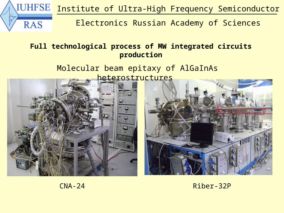
Full technological process of MW integrated circuits production
Molecular beam epitaxy of AlGaInAs heterostructures
CNA-24 Riber-32P
Institute of Ultra-High Frequency Semiconductor Electronics
Russian Academy of Sciences
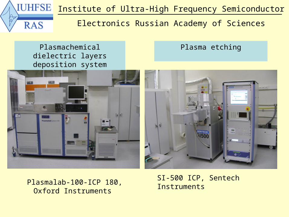
Plasma etchingPlasmachemical dielectric layers deposition system
Plasmalab-100-ICP 180, Oxford Instruments
SI-500 ICP, Sentech Instruments
Institute of Ultra-High Frequency Semiconductor Electronics
Russian Academy of Sciences
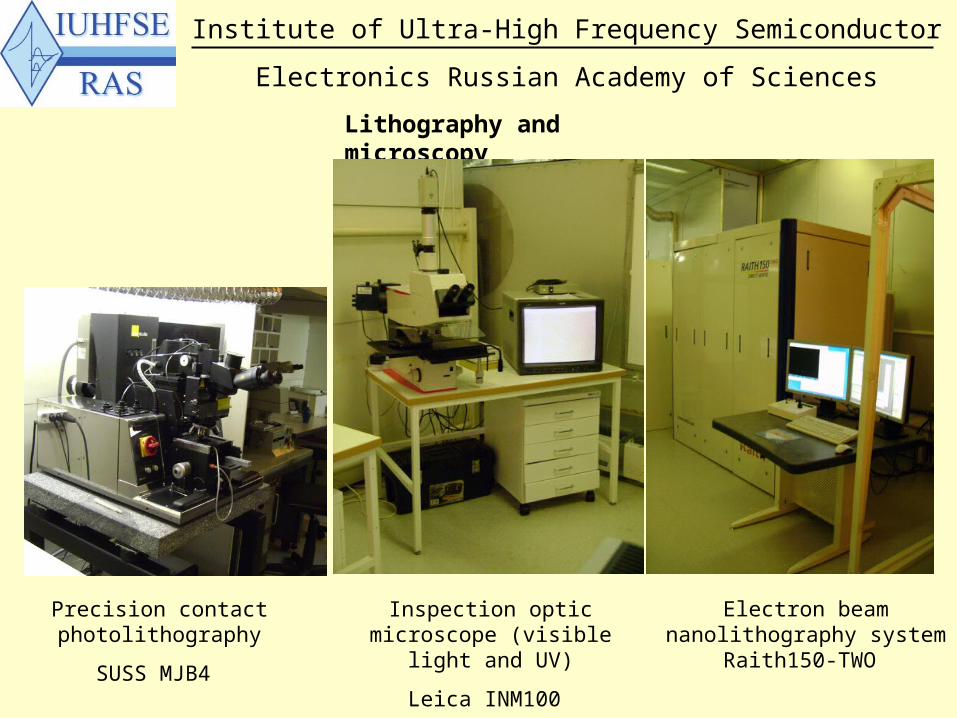
Lithography and microscopy
Precision contact photolithography
SUSS MJB4
Inspection optic microscope (visible light and UV)
Leica INM100
Electron beam nanolithography system
Raith150-TWO
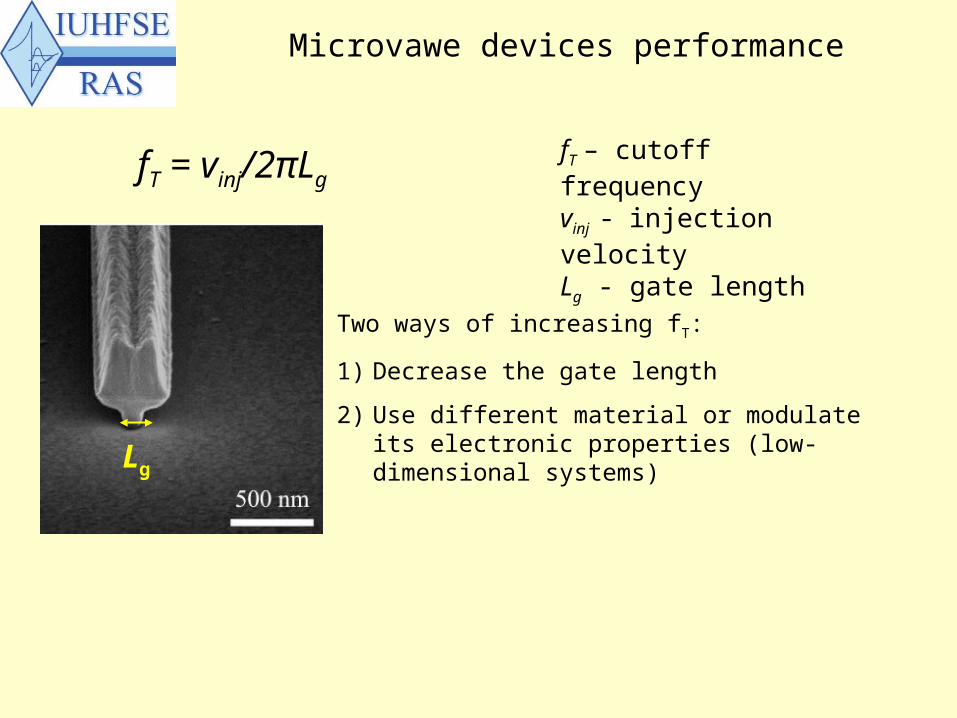
Microvawe devices performance
fT – cutoff frequencyvinj - injection velocityLg - gate length
fT = vinj/2πLg
Lg
Two ways of increasing fT:
1) Decrease the gate length
2) Use different material or modulate its electronic properties (low-dimensional systems)
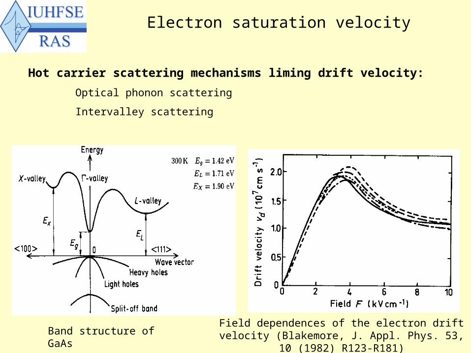
Electron saturation velocity
Field dependences of the electron drift velocity (Blakemore, J. Appl. Phys. 53, 10 (1982) R123-R181)Band structure of GaAs
Hot carrier scattering mechanisms liming drift velocity:
Optical phonon scattering
Intervalley scattering
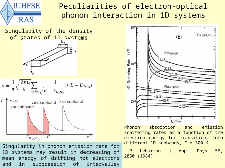
Peculiarities of electron-optical phonon interaction in 1D systems
Phonon absorption and emission scattering rates as a function of the electron energy for transitions into different 1D subbands, T = 300 K
J.P. Leburton, J. Appl. Phys. 56, 2850 (1984)
Singularity of the density of states of 1D systems
Singularity in phonon emission rate for 1D systems may result in decreasing of mean energy of drifting hot electrons and in suppression of intervalley scattering
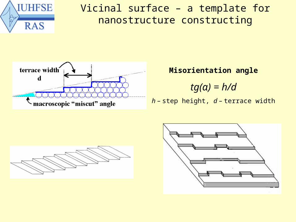
Vicinal surface – a template for nanostructure constructing
Misorientation angle
tg(α) = h/dh – step height, d – terrace width
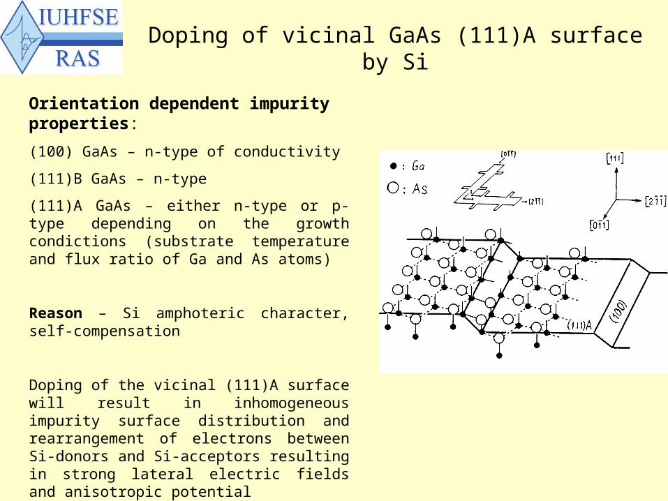
Doping of vicinal GaAs (111)A surface by Si
Orientation dependent impurity properties:
(100) GaAs – n-type of conductivity
(111)B GaAs – n-type
(111)A GaAs – either n-type or p-type depending on the growth condictions (substrate temperature and flux ratio of Ga and As atoms)
Reason – Si amphoteric character, self-compensation
Doping of the vicinal (111)A surface will result in inhomogeneous impurity surface distribution and rearrangement of electrons between Si-donors and Si-acceptors resulting in strong lateral electric fields and anisotropic potential
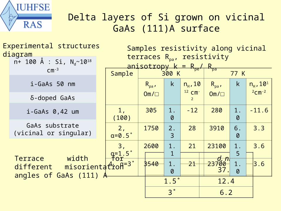
Delta layers of Si grown on vicinal GaAs (111)A surface
n+ 100 Å : Si, Nd~1018 cm-3
i-GaAs 50 nm
δ-doped GaAs
i-GaAs 0,42 um
GaAs substrate (vicinal or singular)
Experimental structures diagram
α d, nm
0.5˚ 37.5
1.5˚ 12.4
3˚ 6.2
Terrace width for different misorientation angles of GaAs (111) A
Samples resistivity along vicinal terraces Rpa, resistivity anisotropy k = Rpe/ Rpa
Sample 300 K 77 K
Rpa,
Om/□
k nH,101
2 cm-2
Rpa,
Om/□
k nH,1012
cm-2
1, (100) 305 1.0 -12 280 1.0 -11.6
2, α=0.5˚ 1750 2.3 28 3910 6.0 3.3
3, α=1.5˚ 2600 1.1 21 23100 1.5 3.6
4, α=3˚ 3540 1.0 21 23700 1.0 3.6
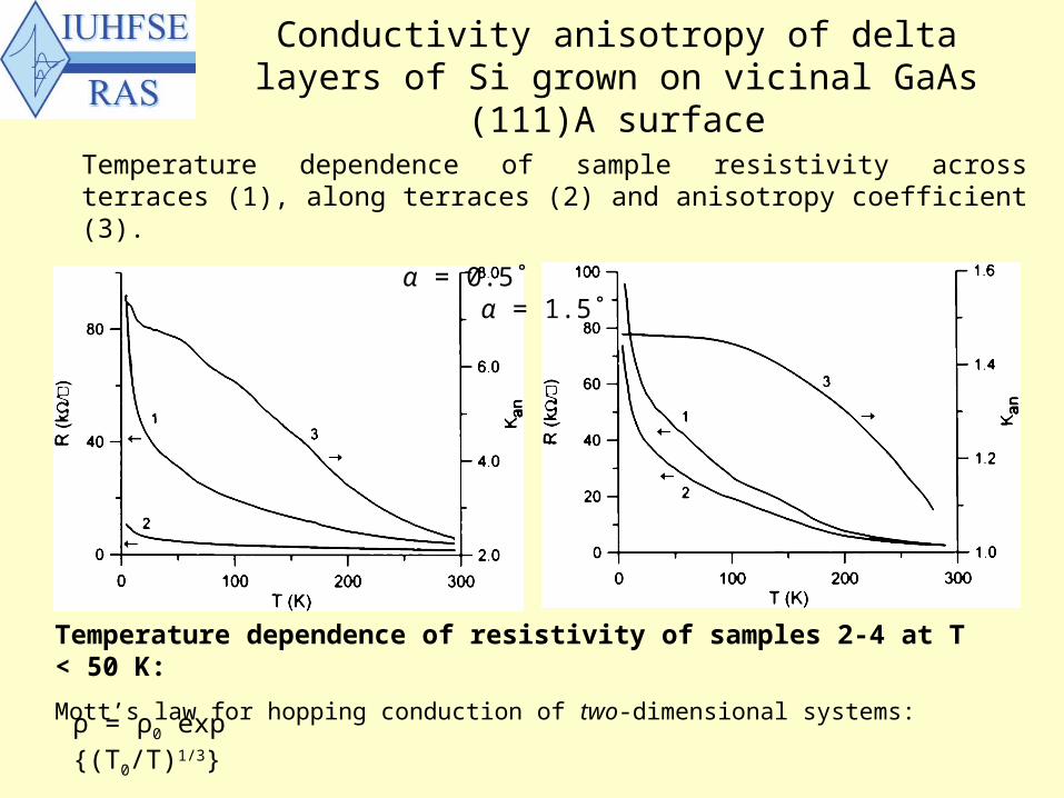
Conductivity anisotropy of delta layers of Si grown on vicinal GaAs (111)A surface
Temperature dependence of sample resistivity across terraces (1), along terraces (2) and anisotropy coefficient (3).
α = 0.5˚ α = 1.5˚
Temperature dependence of resistivity of samples 2-4 at T < 50 K:
Mott’s law for hopping conduction of two-dimensional systems:
ρ = ρ0 exp {(T0/T)1/3}
Application of tin for doping of GaAs vicinal surfaces
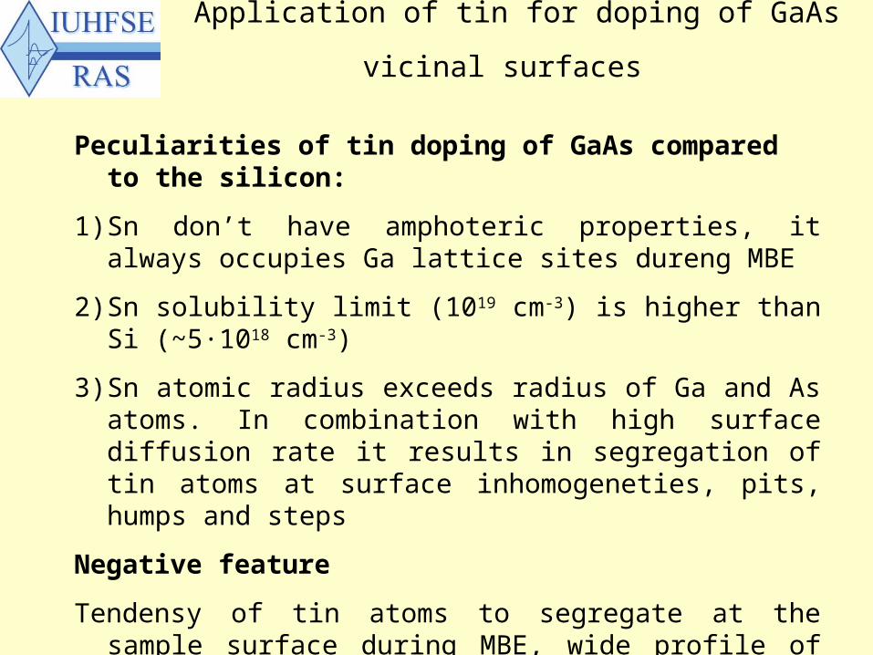
Peculiarities of tin doping of GaAs compared to the silicon:
1) Sn don’t have amphoteric properties, it always occupies Ga lattice sites dureng MBE
2) Sn solubility limit (1019 cm-3) is higher than Si (~5∙1018 cm-3)
3) Sn atomic radius exceeds radius of Ga and As atoms. In combination with high surface diffusion rate it results in segregation of tin atoms at surface inhomogeneties, pits, humps and steps
Negative feature
Tendensy of tin atoms to segregate at the sample surface during MBE, wide profile of Sn delta-doping layers.
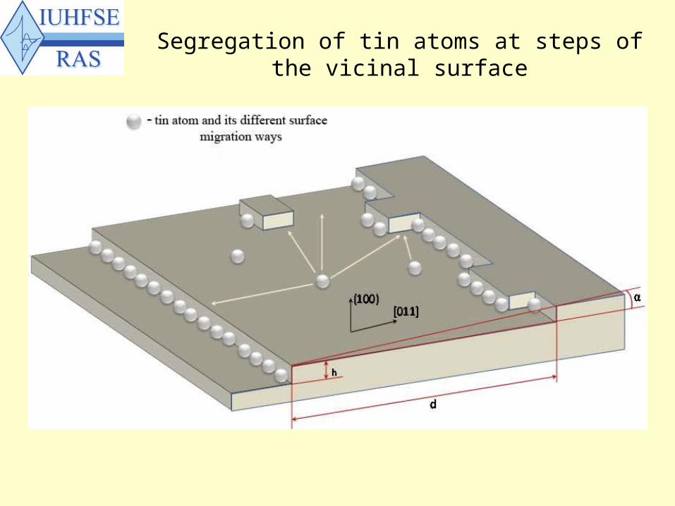
Segregation of tin atoms at steps of the vicinal surface
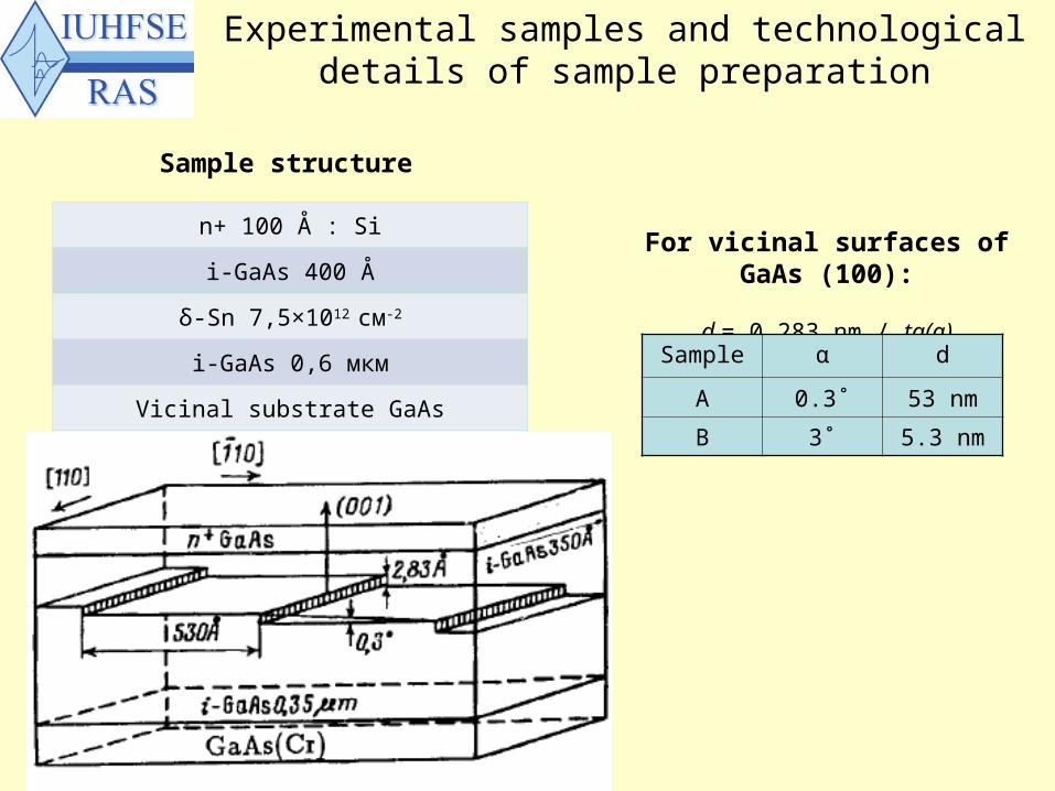
Experimental samples and technological details of sample preparation
n+ 100 Å : Si
i-GaAs 400 Å
δ-Sn 7,5×10¹² см-2
i-GaAs 0,6 мкм
Vicinal substrate GaAs
Sample structure
For vicinal surfaces of GaAs (100):
d = 0.283 nm / tg(α)
Sample α d
A 0.3˚ 53 nm
B 3˚ 5.3 nm
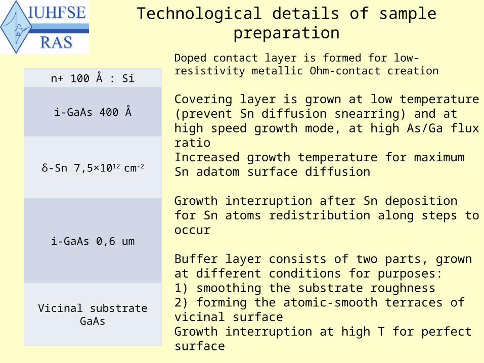
Technological details of sample preparation
n+ 100 Å : Si
i-GaAs 400 Å
δ-Sn 7,5×1012 cm-2
i-GaAs 0,6 um
Vicinal substrate GaAs
Doped contact layer is formed for low-resistivity metallic Ohm-contact creation
Covering layer is grown at low temperature (prevent Sn diffusion snearring) and at high speed growth mode, at high As/Ga flux ratioIncreased growth temperature for maximum Sn adatom surface diffusion
Growth interruption after Sn deposition for Sn atoms redistribution along steps to occur
Buffer layer consists of two parts, grown at different conditions for purposes:1) smoothing the substrate roughness 2) forming the atomic-smooth terraces of vicinal surfaceGrowth interruption at high T for perfect surface
After removal of natural oxide substrate surface is highly rough
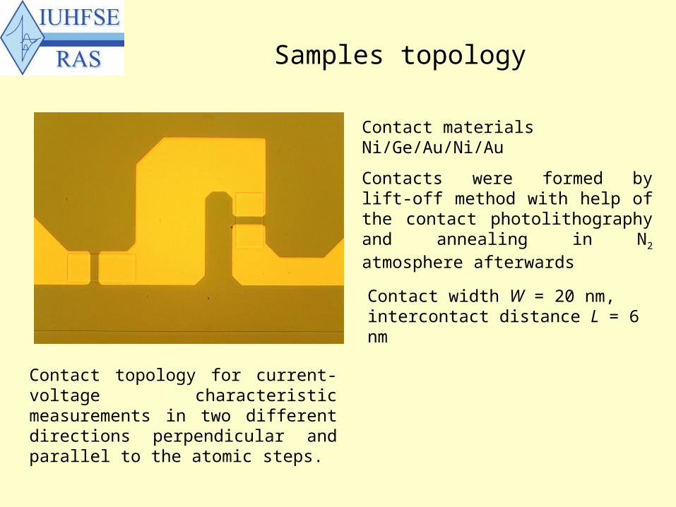
Samples topology
Contact topology for current-voltage characteristic measurements in two different directions perpendicular and parallel to the atomic steps.
Contact materials Ni/Ge/Au/Ni/Au
Contacts were formed by lift-off method with help of the contact photolithography and annealing in N2 atmosphere afterwards
Contact width W = 20 nm, intercontact distance L = 6 nm
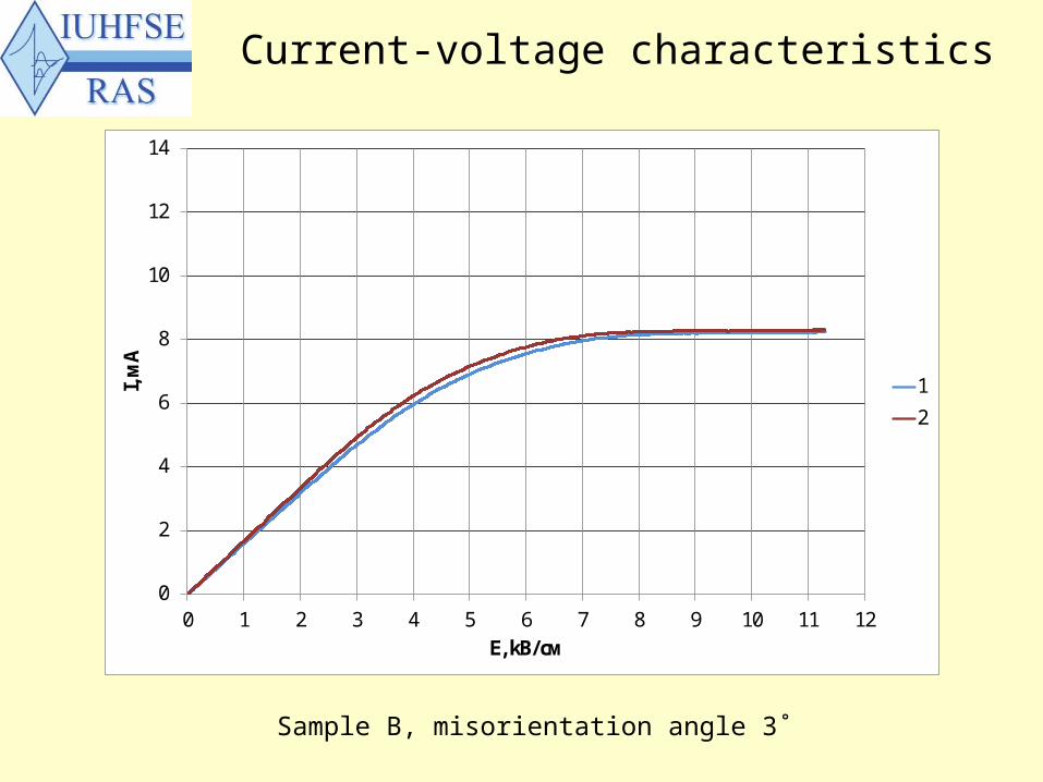
Current-voltage characteristics
0
2
4
6
8
10
12
14
0 1 2 3 4 5 6 7 8 9 10 11 12
I, м
А
E, kВ/см
1
2
Sample B, misorientation angle 3˚
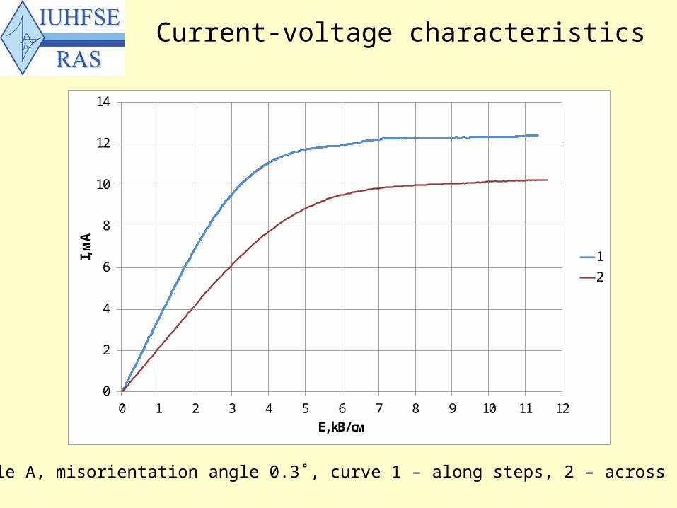
Current-voltage characteristics
0
2
4
6
8
10
12
14
0 1 2 3 4 5 6 7 8 9 10 11 12
I, м
А
E, kВ/см
1
2
Sample A, misorientation angle 0.3˚, curve 1 – along steps, 2 – across steps
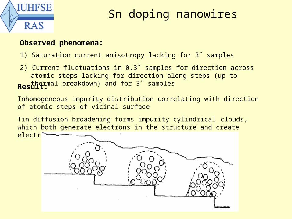
Sn doping nanowires
Observed phenomena:
1) Saturation current anisotropy lacking for 3˚ samples
2) Current fluctuations in 0.3˚ samples for direction across atomic steps lacking for direction along steps (up to thermal breakdown) and for 3˚ samples
Result:
Inhomogeneous impurity distribution correlating with direction of atomic steps of vicinal surface
Tin diffusion broadening forms impurity cylindrical clouds, which both generate electrons in the structure and create electrostatic potential for electron localization
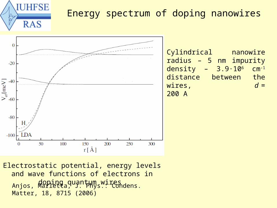
Energy spectrum of doping nanowires
Anjos, Marletta, J. Phys.: Condens. Matter, 18, 8715 (2006)
Electrostatic potential, energy levels and wave functions of electrons in doping quantum wires
Cylindrical nanowire radius – 5 nm impurity density – 3.9∙106 cm-1 distance between the wires, d = 200 A

Thank you for your attention!