introduction to movpe?
TRANSCRIPT
introduction
Introduction to MOVPE?
Metalorganic vapor phase epitaxy (MOVPE) is a process in which monocrystalline compound semiconductor layers are produced by the reaction of molecules in the gas phase on a heated substrate. The substrate provides the crystal`s building plan according to which the atoms order on the surface. The growth process is suitable for the deposition of several ten µm thick and several monolayer thick layers. The deposited compound semiconductor material is employed in a number of device applications due to its direct band gap: optoelectronic devices such as laser or light emitting diodes or extraterrestrial solar cells and on the other hand electronic devices such as high frequency transistors. Since large areas are used for these device applications, deposition techniques are industrially employed which ensure a high throughput. The MOVPE meets these needs and is therefore the preferred deposition technique for industry.
Vapor phase epitaxy is determined by thermodynamics, kinetics and hydrodynamics. The thermodynamics of the growth process describes the direction in which the reactions take place and is the driving force for layer growth. The kinetics of growth describes all gas phase and surface reactions, which take place in the reactor. The hydrodynamics of the growth process describes the mass transport of the molecules in the gas phase as well as the temperature gradient, the velocity profile and the total pressure in the reactor. An Arrhenius plot can best demonstrate the overall growth process. Such a plot is shown schematically below. Three different regimes can be
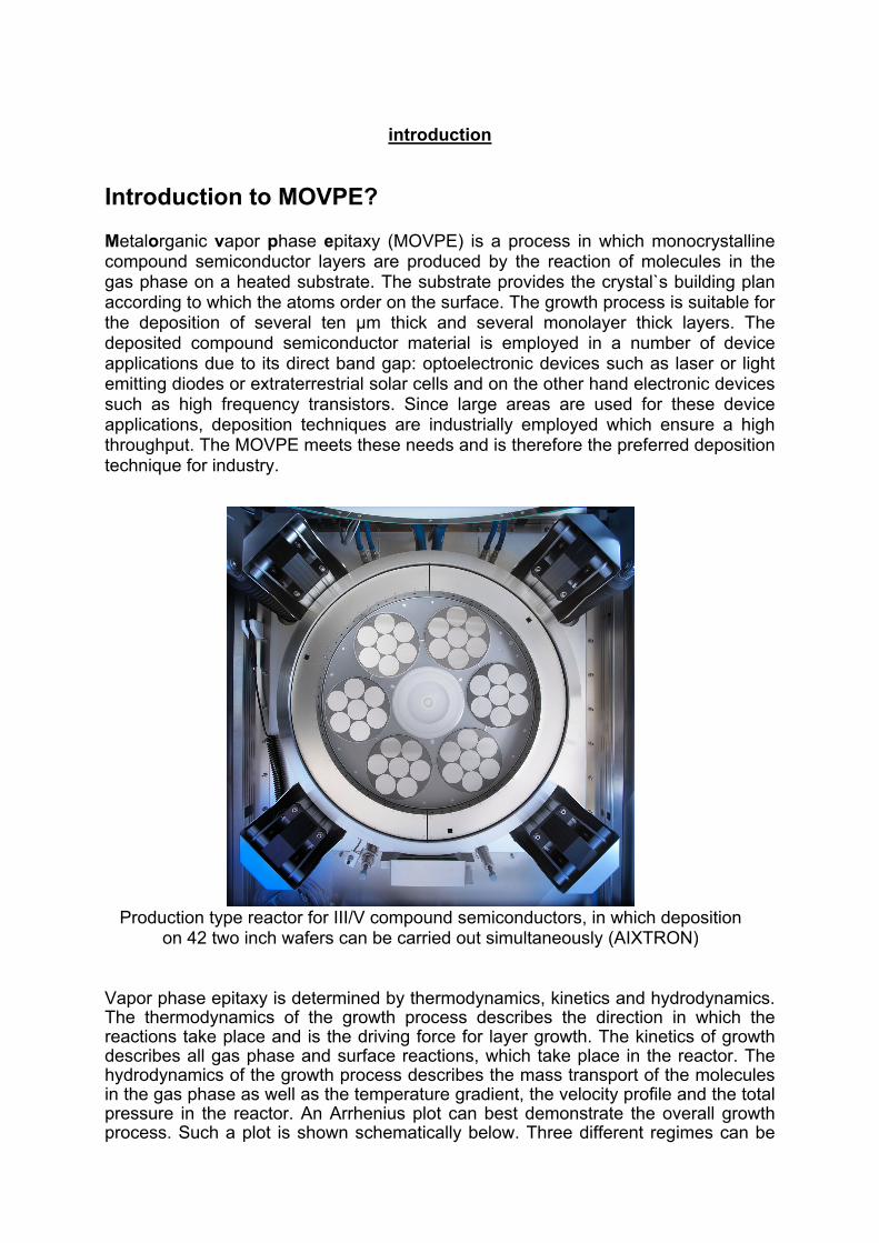
Production type reactor for III/V compound semiconductors, in which deposition
on 42 two inch wafers can be carried out simultaneously (AIXTRON)

distinguished. In the low temperature region, a linear dependence is found between reciprocal temperature and reciprocal growth rate. Growth is determined by the rate of the slowest reaction. From the slope of the curve, the activation energy – Ea - of this reaction is determinable. In the intermediate temperature range, the slope is close to 0 which means that not the kinetics but the access of the reactive species to the sample surface limits growth. At still higher temperatures, a negative slope is find, which can mean that the chemical thermodynamics determines growth (reverse reaction), other reaction pathways become dominant or that pre-deposition takes place. It becomes very clear that the deposition temperature has an enormous impact on growth. Preferentially growth is carried out in the diffusion controlled growth regime since small variations in substrate temperature do not have a big impact on growth. Typical growth temperatures are between 600 and 700°C for group III arsenides and phosphides as well as InN and above 1000°C for (AlGa)N. Usually an excess of the group V component is injected into the reactor since the III/V compound semiconductors tend to incongruently lose the group V component by evaporation. In addition to the partial pressure of the group V hydrogen compounds needed for growth a certain amount is used to stabilize the growing surface. Therefore the group III growth compound mainly determines growth.
The growth process A carrier gas is used to transport the gaseous organic group III source compounds – conventionally these are trimethylaluminuum (TMAl), trimethylgallium (TMGa), trimethylindium (TMIn), ((III)(CH3)3) – and the group V hydrogen compounds (VH3) – Ammoniak (NH3), Phosphin (PH3), und Arsin (AsH3) – into the reactor. They react partially in the gas phase and diffuse to the heated substrate surface, where the reactive species adsorb and last decomposition reactions take place to produce the intended compound. The gaseous products desorb and diffuse away.
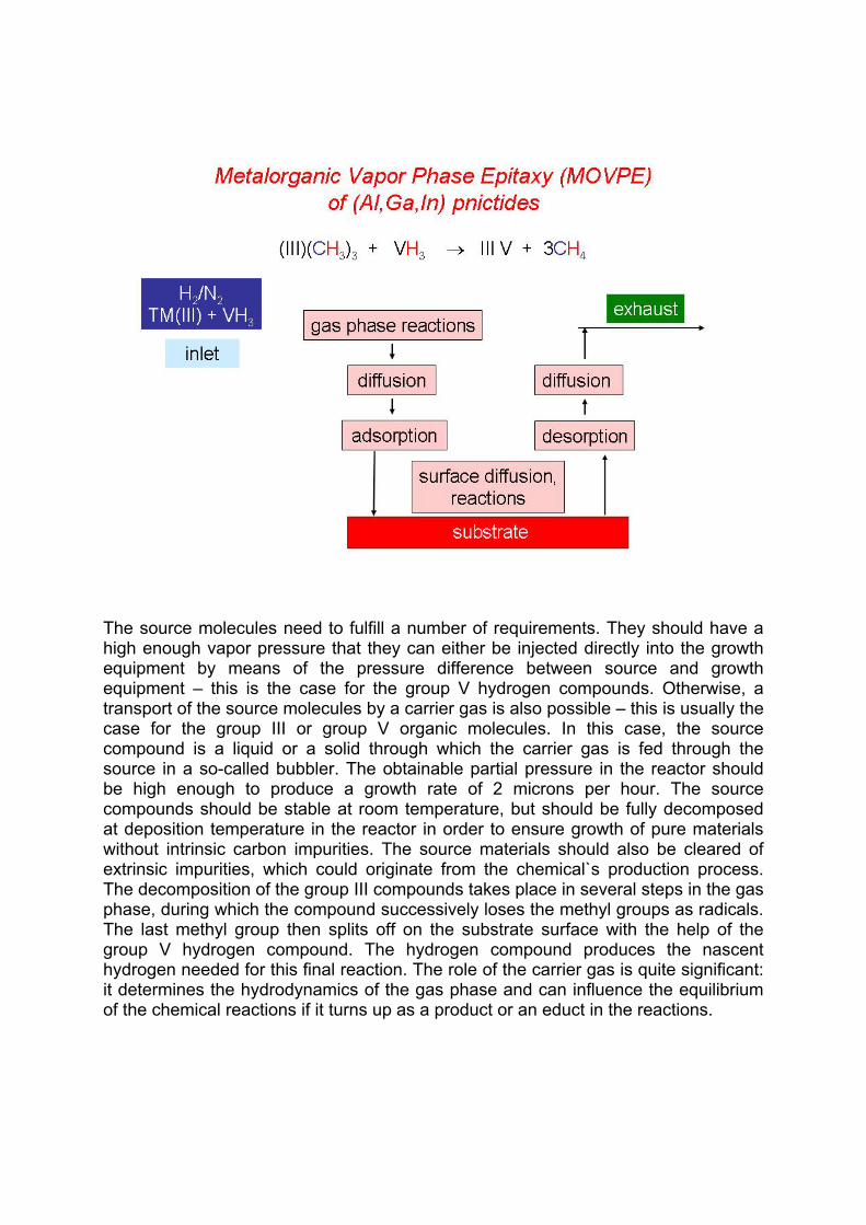
The source molecules need to fulfill a number of requirements. They should have a high enough vapor pressure that they can either be injected directly into the growth equipment by means of the pressure difference between source and growth equipment – this is the case for the group V hydrogen compounds. Otherwise, a transport of the source molecules by a carrier gas is also possible – this is usually the case for the group III or group V organic molecules. In this case, the source compound is a liquid or a solid through which the carrier gas is fed through the source in a so-called bubbler. The obtainable partial pressure in the reactor should be high enough to produce a growth rate of 2 microns per hour. The source compounds should be stable at room temperature, but should be fully decomposed at deposition temperature in the reactor in order to ensure growth of pure materials without intrinsic carbon impurities. The source materials should also be cleared of extrinsic impurities, which could originate from the chemical`s production process. The decomposition of the group III compounds takes place in several steps in the gas phase, during which the compound successively loses the methyl groups as radicals. The last methyl group then splits off on the substrate surface with the help of the group V hydrogen compound. The hydrogen compound produces the nascent hydrogen needed for this final reaction. The role of the carrier gas is quite significant: it determines the hydrodynamics of the gas phase and can influence the equilibrium of the chemical reactions if it turns up as a product or an educt in the reactions.
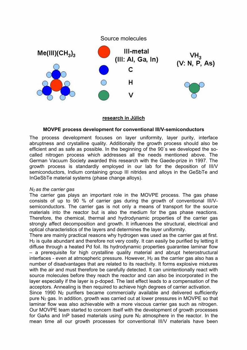
Source molecules
research in Jülich
MOVPE process development for conventional III/V-semiconductors The process development focuses on layer uniformity, layer purity, interface abruptness and crystalline quality. Additionally the growth process should also be efficient and as safe as possible. In the beginning of the 90`s we developed the so-called nitrogen process which addresses all the needs mentioned above. The German Vacuum Society awarded this research with the Gaede-prize in 1997. The growth process is standardly employed in our lab for the deposition of III/V semiconductors, Indium containing group III nitrides and alloys in the GeSbTe and InGeSbTe material systems (phase change alloys). N2 as the carrier gas The carrier gas plays an important role in the MOVPE process. The gas phase consists of up to 90 % of carrier gas during the growth of conventional III/V-semiconductors. The carrier gas is not only a means of transport for the source materials into the reactor but is also the medium for the gas phase reactions. Therefore, the chemical, thermal and hydrodynamic properties of the carrier gas strongly affect decomposition and growth. It influences the structural, electrical and optical characteristics of the layers and determines the layer uniformity. There are mainly practical reasons why hydrogen was used as the carrier gas at first. H2 is quite abundant and therefore not very costly. It can easily be purified by letting it diffuse through a heated Pd foil. Its hydrodynamic properties guarantee laminar flow – a prerequisite for high crystalline quality material and abrupt heterostructural interfaces - even at atmospheric pressure. However, H2 as the carrier gas also has a number of disadvantages that are related to its reactivity. It forms explosive mixtures with the air and must therefore be carefully detected. It can unintentionally react with source molecules before they reach the reactor and can also be incorporated in the layer especially if the layer is p-doped. The last effect leads to a compensation of the acceptors. Annealing is then required to achieve high degrees of carrier activation. Since 1990 N2 purifiers became commercially available and delivered sufficiently pure N2 gas. In addition, growth was carried out at lower pressures in MOVPE so that laminar flow was also achievable with a more viscous carrier gas such as nitrogen. Our MOVPE team started to concern itself with the development of growth processes for GaAs and InP based materials using pure N2 atmosphere in the reactor. In the mean time all our growth processes for conventional III/V materials have been
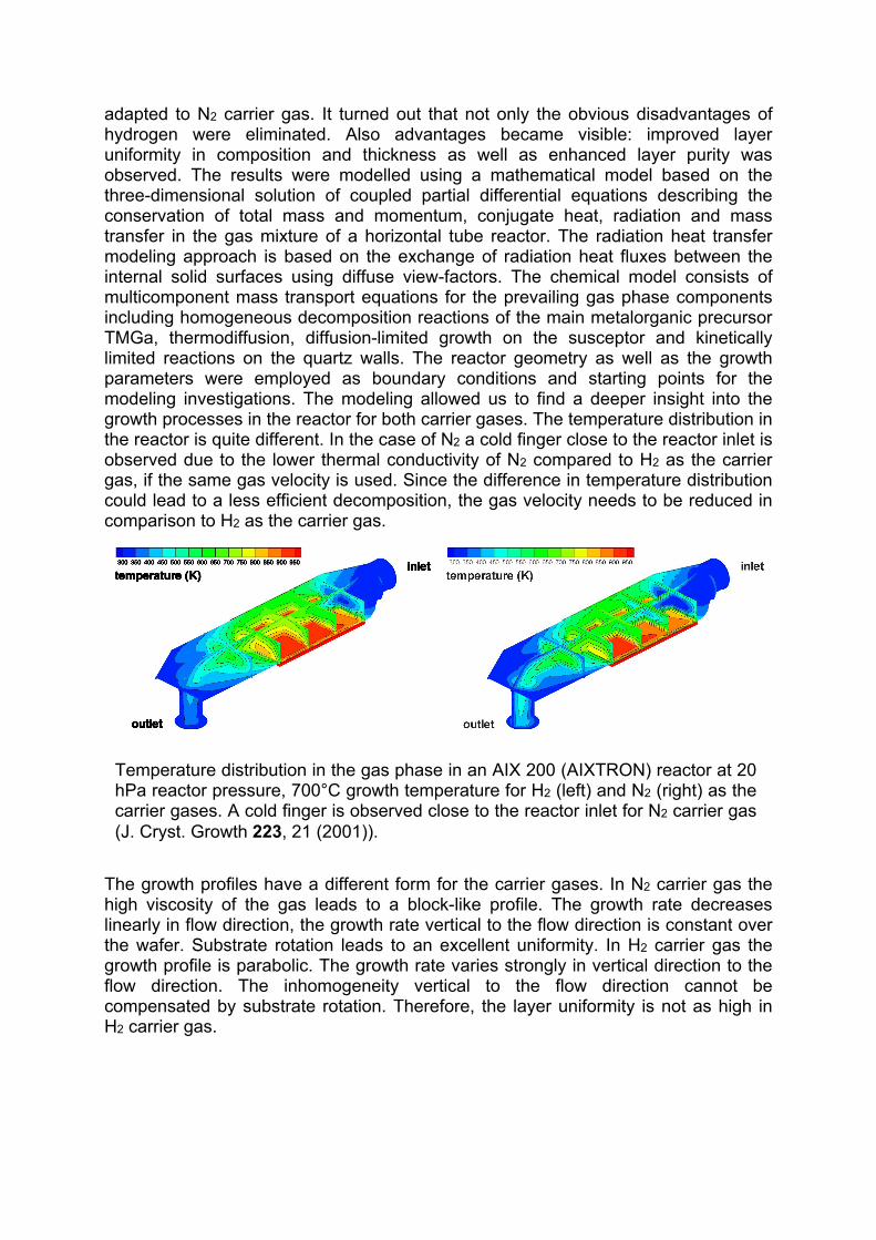
adapted to N2 carrier gas. It turned out that not only the obvious disadvantages of hydrogen were eliminated. Also advantages became visible: improved layer uniformity in composition and thickness as well as enhanced layer purity was observed. The results were modelled using a mathematical model based on the three-dimensional solution of coupled partial differential equations describing the conservation of total mass and momentum, conjugate heat, radiation and mass transfer in the gas mixture of a horizontal tube reactor. The radiation heat transfer modeling approach is based on the exchange of radiation heat fluxes between the internal solid surfaces using diffuse view-factors. The chemical model consists of multicomponent mass transport equations for the prevailing gas phase components including homogeneous decomposition reactions of the main metalorganic precursor TMGa, thermodiffusion, diffusion-limited growth on the susceptor and kinetically limited reactions on the quartz walls. The reactor geometry as well as the growth parameters were employed as boundary conditions and starting points for the modeling investigations. The modeling allowed us to find a deeper insight into the growth processes in the reactor for both carrier gases. The temperature distribution in the reactor is quite different. In the case of N2 a cold finger close to the reactor inlet is observed due to the lower thermal conductivity of N2 compared to H2 as the carrier gas, if the same gas velocity is used. Since the difference in temperature distribution could lead to a less efficient decomposition, the gas velocity needs to be reduced in comparison to H2 as the carrier gas.
The growth profiles have a different form for the carrier gases. In N2 carrier gas the high viscosity of the gas leads to a block-like profile. The growth rate decreases linearly in flow direction, the growth rate vertical to the flow direction is constant over the wafer. Substrate rotation leads to an excellent uniformity. In H2 carrier gas the growth profile is parabolic. The growth rate varies strongly in vertical direction to the flow direction. The inhomogeneity vertical to the flow direction cannot be compensated by substrate rotation. Therefore, the layer uniformity is not as high in H2 carrier gas.
Temperature distribution in the gas phase in an AIX 200 (AIXTRON) reactor at 20 hPa reactor pressure, 700°C growth temperature for H2 (left) and N2 (right) as the carrier gases. A cold finger is observed close to the reactor inlet for N2 carrier gas (J. Cryst. Growth 223, 21 (2001)).
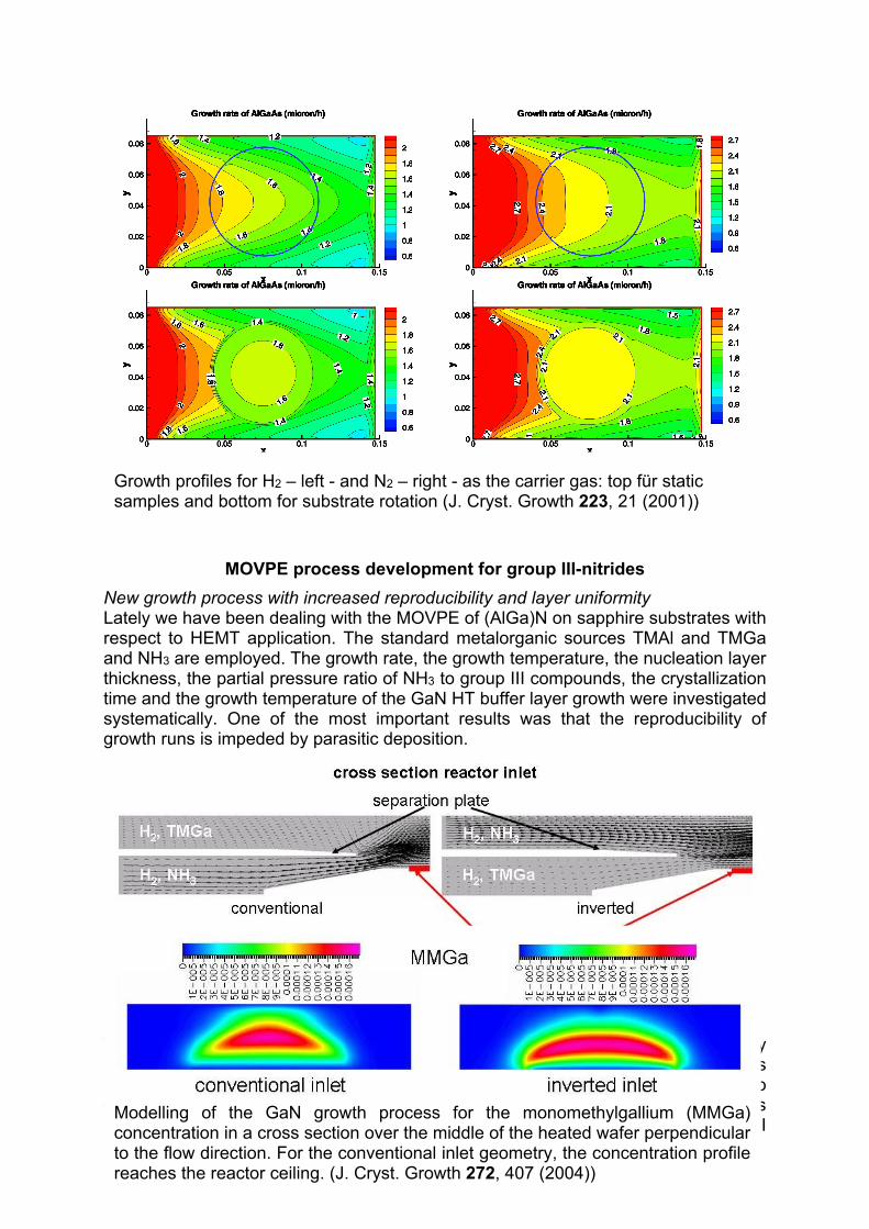
MOVPE process development for group III-nitrides New growth process with increased reproducibility and layer uniformity Lately we have been dealing with the MOVPE of (AlGa)N on sapphire substrates with respect to HEMT application. The standard metalorganic sources TMAl and TMGa and NH3 are employed. The growth rate, the growth temperature, the nucleation layer thickness, the partial pressure ratio of NH3 to group III compounds, the crystallization time and the growth temperature of the GaN HT buffer layer growth were investigated systematically. One of the most important results was that the reproducibility of growth runs is impeded by parasitic deposition.
This insight was possible by using in situ optical methods during growth and by employing a method with which the growth temperature for transparent substrates can be determined. We developed a growth process which hinders materials to deposit on especially the reactor ceiling. In our reactor type a separation plate was inserted in the gas inlet which allows the separate injection of ammonia and group III
Comparison of the conventional gas inlet to the inverted gas inlet in which the metalorganic compounds are injected closer to the heated substrate (J. Cryst. Growth 272, 407 (2004))
Growth profiles for H2 – left - and N2 – right - as the carrier gas: top für static samples and bottom for substrate rotation (J. Cryst. Growth 223, 21 (2001))
Modelling of the GaN growth process for the monomethylgallium (MMGa) concentration in a cross section over the middle of the heated wafer perpendicular to the flow direction. For the conventional inlet geometry, the concentration profile reaches the reactor ceiling. (J. Cryst. Growth 272, 407 (2004))

compounds into the reactor. The plate partitions the injector into two channels. Conventionally, ammonia is led into the reactor through the lower, the metalorganic sources through the upper.
In MOVPE, the partially decomposed group III compound for Ga-containing compounds is monomethylgallium (MMGa), which mainly induces growth. Since TMGa is injected through the upper channel close to the reactor ceiling for the conventional growth process and the temperature of the unintentionally heated reactor ceiling is high enough to induce decomposition, the concentration of MMG is high near the ceiling. Modelling experiments demonstrate that the growth of of GaN is four times as high on the reactor ceiling upstream of the wafer than on the substrate itself. Our growth process inverts the gas injection. A comparison with modelling shows that parasitic deposition is strongly reduced by a factor of 3.5.
The further focus of our work is directed towards the interpretation of in situ optical data obtained during epitaxy and their correlation with ex situ obtained structural, morphological and electical layer characteritiscs and the optimization of the growth process with respect to layer uniformity for the conventional as well as for the inverted growth process.
Development and application of in situ optical characterization techniques Deposition techniques, which are carried out in UHV conditions have the advantage that a great number of characterizations techniques are used with which growth is observed and controlled in situ. Only rather recently in the last decade, optical techniques have been developed which can also be employed for CVD-processes. In the mean time, they have become state of the art in research and industrial production. They also make a better understanding of growth parameter influences possible. Together with our industrial partner LayTec, Berlin, we have taken part in the further exploitation and development of optical sensors for growth if it was necessary for our growth task. We were able to find the origin of non-reproducibility of nitrides growth in our reactor. The necessity of temperature determination for transparent substrates became apparent. To this end, a temperature determination method was developed and implemented. This method allowed us to also determine the unintentional influence of carrier gas, reactor pressure, rotation gas, gas velocity as well as parasitic reactor deposition on substrate temperature. The influence of the intentionally varied growth parameter became accessible. In addition, a method was developed with which the composition of AlGaN-layers could be determined from the
Modelling of the GaN growth process of the parasitic deposition on the reactor ceiling above the substrate (black circle). For the conventional growth process, the growth rate of parasitic deposition is three times as high as for our inverted process (J. Cryst. Growth 272, 407 (2004)).

transients. An optical model was introduced with which the influence of roughness on different size scales can be understood.
Influence of roughness on reflectance transients for different roughness size scales (Journal de Physique IV, 132 (2006), 177 – 183)
On site characterization techniques
The epitaxial layers are standardly characterized by a number of techniques:
• optical microscopy - a Nomarski-interference microscope is used for the inspection of surface morphology;
• X-ray diffractometry (XRD) for the determination of crystal quality, composition, layer thickness and relaxation;
• Hall-effect measurements at room (300K) and liquid N2 temperature (77K) for the determination of carrier concentration and carrier mobility; T-dependent measurements can also be carried out down to liquid He temperature (4K);
• Atomic force microscopy (AFM) for the study of morphology; • Scanning electron microscopy (SEM) for the study of morphology and fort he
determination of layer thickness; • Photoluminescence (PL) at low (2K) and room temperature (300K) for the
determination of crystal quality and imperfection, composition, impurities, ordering effects;
• SIMS (secondary ion mass spectrometry) for the investigation of doping incorporation;
• Rutherford Backscattering Spectrometry (RBS) for the characterization of crystal quality and for the determination of group III nitride composition