rf-molecular beam epitaxy growth and properties of inn and ... · in contrast, molecular beam...
TRANSCRIPT

Printed with permission of The Institute of Pure and Applied Physics (IPAP)
Invited Review Paper
JAPANESE JOURNAL OF APPLIED PHYSICS Vol.42 (2003) pp.2549-2559JAPANESE JOURNAL OF APPLIED PHYSICS Vol.42 (2003) pp.2549-2559Part1 No.5A, May 2003 No.5A, May 2003
Invited Review PaperInvited Review Paper
4 JSAP International No.9 (January 2004)
The fundamental band gap of InN has
been thought to be about 1.9 eV for a long
time. Recent developments of metalorganic
vapor phase epitaxy (MOVPE) and RF-molec-
ular beam epitaxy (RF-MBE) growth technolo-
gies have made it possible to obtain high-
quality InN films. A lot of experimental results
have been presented very recently, suggesting
that the true band-gap energy of InN should
be less than 1.0 eV. In this paper, we review
the results of the detailed study of RF-MBE
growth conditions for obtaining high-quality
InN films. The full widths at half maximum
(FWHMs) of ω -mode X-ray diffraction (XRD),
ω–2θ mode XRD and E2 (high-frequency)-
phonon-mode peaks in the Raman scatter-
ing spectrum of the grown layer were 236.7
arcsec, 28.9 arcsec and 3.7 cm-1, respectively.
The carrier concentration and room tempera-
ture electron mobility were 4.9 × 1018cm-3
and 1130 cm2/Vs, respectively. Photolumines-
cence and optical absorption measurements
of these high-quality InN films have clearly
demonstrated that the fundamental band
gap of InN is about 0.8 eV. Studies on the
growth and characterization of InGaN alloys
over the entire alloy composition further sup-
ported that the fundamental band gap of InN
is about 0.8 eV.
KEYWORDS: InN, InGaN, band gap, RF-
MBE, characterization, PL, op-
tical absorption, XRD, EXAFS,
Raman scattering
1. IntroductionInN is a very attractive material for future
optical and electronic devices. This is because
of its outstanding material properties such as
smallest effective mass, largest mobility, high-
est peak and saturation velocities, and small-
est direct band gap in nitride semiconductors.
However, until now, InN has been the least
studied of nitride semiconductors. This is
mainly due to the difficulty in obtaining high-
quality InN crystals, which is due to the low
dissociation temperature, high equilibrium
vapor pressure of nitrogen molecules and the
lack of suitable substrates for InN.
Studies on InN started in the beginning
of the 20th century with an attempt to grow
bulk InN from a melt.1) The attempt was not
successful because of the low dissociation
temperature and high vapor pressure of nitro-
gen molecules.2)
The next step in growing InN moved be-
yond the equilibrium approach to the non-
equilibrium approach using various substrate
materials by various growth methods includ-
ing DC, RF, and magnetron sputtering.3–5)
The InN films obtained by these methods in
the 1970s and 1980s were all polycrystalline,
some with an aligned orientation along the
c-axis; the films also contained an extremely
high defect density.
The physical parameters of InN were de-
termined using these crystals. The first esti-
mated direct band gap was about 1.9 eV.6)
However, other studies reported values rang-
ing from 1.7 to 3.1 eV.3,7–11) The most com-
monly cited measurement on optical ab-
sorption is that of Tansley and Foley;12) they
reported band gap energy of 1.89 eV at room
temperature.
In the late 1980s, improvements in
growth techniques have made it possible to
obtain single-crystalline InN. Single-crystalline
InN was reported by Matsuoka et al.13) for the
first time in 1989 using metalorganic vapor
phase epitaxy (MOVPE). Subsequently, several
efforts14,15) were made to improve the qual-
ity of InN and high-quality films with carrier
concentrations on the order of 1018 cm-3 and
mobilities of 730 cm2/ Vs16) were obtained.
Growth by MOVPE, however, has an inher-
ent disadvantage because it must satisfy the
conditions for NH3 pyrolysis and InN dissocia-
tion, which impose conflicting temperature
requirements.
In contrast, molecular beam epitaxy (MBE)
equipped with an RF plasma source has an
essential advantage over MOVPE for obtain-
ing high-quality InN. In this growth method,
neutral and ionized excited-state nitrogen
atoms and molecules can be generated sepa-
rately by plasma sources. Thus, the crystal
growth temperature can be set independent-
ly without considering the nitrogen source.
The first attempt to grow single-crystal-
line InN by the RF-MBE method was reported
by Hoke et al. in 1991.17) Improvements in
crystal quality were realized by various tech-
niques such as insertion of low-temperature
GaN,18) AlN,19) and InN20) buffer layers. Within
a relatively short period of time, MBE growth
studies produced high-quality films with re-
sidual electron concentrations of 1.6 × 10¹⁸
cm-3 and a room temperature mobility of
1180 cm2/ Vs.18) Such rapid progress is proba-
bly due to the inherent advantage of the MBE
growth method.
Photoluminescence (PL) and optical ab-
sorption were used to study single-crystalline
InN films that were grown using MOVPE and
MBE. These studies revealed that the funda-
mental band gap of single-crystalline InN was
about 0.8 eV21–25) instead of 1.9 eV, deter-
mined by optical absorption using polycrystal-
line InN.
In this paper, we review the detailed
studies of InN and InGaN growth by RF-MBE.
Department of Photonics, Ritsumeikan University, 1-1-1 Noji-Higashi, Kusatsu, Shiga 525-8577, Japan(Received January 10, 2003; accepted for publication March 11, 2003)©2003 The Japan Society of Applied Physics
RF-Molecular Beam Epitaxy Growth and Properties of InN and Related AlloysRF-Molecular Beam Epitaxy Growth and Properties of InN and Related AlloysYasushi NANISHI, Yoshiki SAITO and Tomohiro YAMAGUCHI
JSAP International No.9 (January 2004) 5
First, fundamental studies on basic growth
processes are reviewed; these include the
initial growth stage, two-step growth pro-
cesses, the precise control of V/ III ratio, and
the resultant crystal properties of the grown
films. Then we describe how precise control
of growth temperature and insertion of low-
temperature intermediate layers can be used
to grow higher-quality InN films. Our group
used a wide variety of techniques to deter-
mine the crystallographic, electrical, and op-
tical properties of high-quality InN films. The
techniques include X-ray diffraction (XRD), in
situ reflection high-energy electron diffrac-
tion (RHEED), extended X-ray absorption fine
structure (EXAFS), Rutherford backscattering
(RBS), atomic force microscopy (AFM), coaxial
impact-collision ion scattering spectroscopy
(CAICISS), Hall effect measurements, PL, cath-
ode-luminescence (CL), optical absorption,
photo modulated reflectance, infrared spec-
troscopic ellipsometry, and Raman scattering.
Typical results are described in §4.
Finally, InGaN films were grown over the
entire range of alloy composition on sapphire
substrates by inserting InN buffer layers. Re-
sults on optical absorption, CL, and PL mea-
surements are presented.
2. Fundamental Study of Growth Process
2.1 Growth system and standard growth conditions
The growth of InN by RF-MBE was carried
out in an MBE growth chamber equipped
with a high-speed turbo-molecular pump
(1500 liter/ s) that evacuated the chamber
up to 1 × 10⁻¹⁰ Torr. This MBE system is also
equipped with a SVTA radical cell (model 2.75)
to serve as the nitrogen source. The sub-
strates used were mainly (0001) sapphire sub-
strates. The back surface was coated with a
1-µm-thick layer of molybdenum. They were
set on an In-free molybdenum holder after
being cleaned with organic solvents. High-
purity (6N) In and Ga were used as group III
materials and were evaporated from standard
effusion cells. High-purity N2 gas (6N) was
supplied to the RF plasma cell after passing
through a Saes Getter purifier (model Mono-
torr Phase II 3000) to eliminate impurities
including H2O, H2, O2, CO, and CO2 gases.
Nitrogen gas of 2 sccm, which produced a
pressure of 1 × 10⁻⁴ Torr, was supplied for InN
growth. The typical growth rate of InN was
approximately 500 nm/h. Growth tempera-
tures were carefully monitored with a pyrom-
eter at each growth run.
2.2 Initial growth stageIn contrast to GaN and AlN that grow
on sapphire substrates with their a-axis ori-
entation rotated 30º to become [101–0]GaN,AlN
|| [112–0]sapphire, InN tends to grow with both
[101–0]InN || [112
–0]sapphire and [112
–0]InN ||
[112–0]sapphire and easily form polycrystals.26)
This is due to the fact that lattice mismatch
values of these two cases are very close,
which is not the case for GaN and AlN, where
lattice mismatch is much smaller when the
a-axis rotates by 30º to become [101–0]GaN,AlN
|| [112–0]sapphire. The lattice mismatch values
of nitride semiconductors and sapphire sub-
strates for these two cases are compared in
Table l.
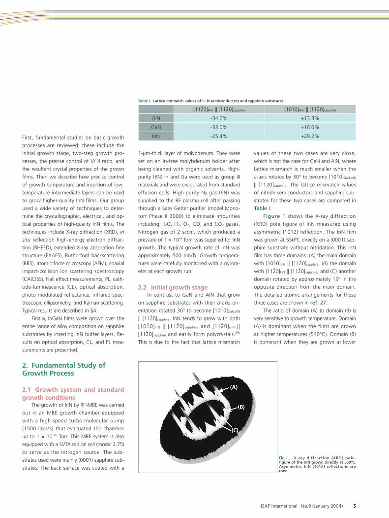
Figure 1 shows the X-ray diffraction
(XRD) pole figure of InN measured using
asymmetric {101–2} reflection. The InN film
was grown at 550ºC directly on a (0001) sap-
phire substrate without nitridation. This InN
film has three domains: (A) the main domain
with [101–0]InN || [112
–0]sapphire, (B) the domain
with [112–0]InN || [112
–0]sapphire, and (C) another
domain rotated by approximately 19º in the
opposite direction from the main domain.
The detailed atomic arrangements for these
three cases are shown in ref. 27.
The ratio of domain (A) to domain (B) is
very sensitive to growth temperature. Domain
(A) is dominant when the films are grown
at higher temperatures (540ºC). Domain (B)
is dominant when they are grown at lower
Table I. Lattice mismatch values of III-N semiconductors and sapphire substrates.
[112–0]III-N || [112
–0]sapphire [101
–0]III-N || [112
–0]sapphire
AlN -34.6% +13.3%
GaN -33.0% +16.0%
InN -25.4% +29.2%
Fig.1. X-ray diffraction (XRD) pole-fi gure of the InN grown directly at 550ºC. Asymmetric InN {101
–2} refl ections are
used.
6 JSAP International No.9 (January 2004)
0 50 100 150 200 250 300 350φ [º ]
Inte
nsi
ty (
arb
. un
its)
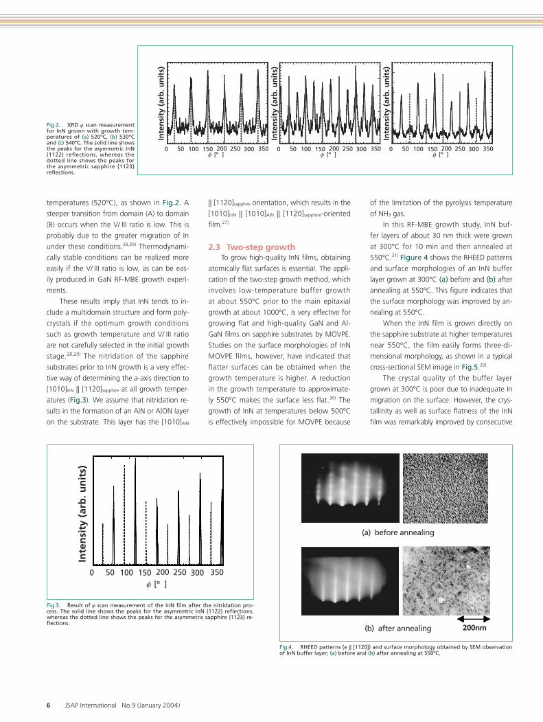
temperatures (520ºC), as shown in Fig.2. A
steeper transition from domain (A) to domain
(B) occurs when the V/ III ratio is low. This is
probably due to the greater migration of In
under these conditions.28,29) Thermodynami-
cally stable conditions can be realized more
easily if the V/ III ratio is low, as can be eas-
ily produced in GaN RF-MBE growth experi-
ments.
These results imply that InN tends to in-
clude a multidomain structure and form poly-
crystals if the optimum growth conditions
such as growth temperature and V/ III ratio
are not carefully selected in the initial growth
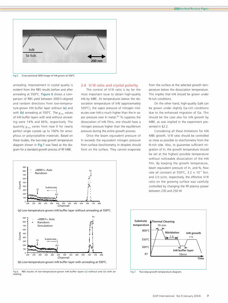
stage.28,29) The nitridation of the sapphire
substrates prior to InN growth is a very effec-
tive way of determining the a-axis direction to
[101–0]InN || [112
–0]sapphire at all growth temper-
atures (Fig.3). We assume that nitridation re-
sults in the formation of an AlN or AlON layer
on the substrate. This layer has the [101–0]AlN
|| [112–0]sapphire orientation, which results in the
[101–0]InN || [101
–0]AlN || [112
–0]sapphire-oriented
film.27)
2.3 Two-step growthTo grow high-quality InN films, obtaining
atomically flat surfaces is essential. The appli-
cation of the two-step growth method, which
involves low-temperature buffer growth
at about 550ºC prior to the main epitaxial
growth at about 1000ºC, is very effective for
growing flat and high-quality GaN and Al-
GaN films on sapphire substrates by MOVPE.
Studies on the surface morphologies of InN
MOVPE films, however, have indicated that
flatter surfaces can be obtained when the
growth temperature is higher. A reduction
in the growth temperature to approximate-
ly 550ºC makes the surface less flat.30) The
growth of InN at temperatures below 500ºC
is effectively impossible for MOVPE because
of the limitation of the pyrolysis temperature
of NH3 gas.
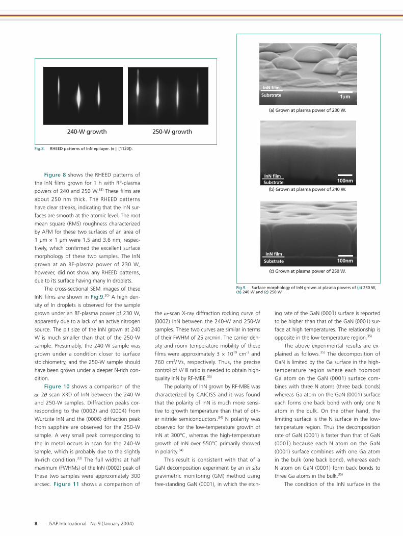
In this RF-MBE growth study, InN buf-
fer layers of about 30 nm thick were grown
at 300ºC for 10 min and then annealed at
550ºC.31) Figure 4 shows the RHEED patterns
and surface morphologies of an InN buffer
layer grown at 300ºC (a) before and (b) after
annealing at 550ºC. This figure indicates that
the surface morphology was improved by an-
nealing at 550ºC.
When the InN film is grown directly on
the sapphire substrate at higher temperatures
near 550ºC, the film easily forms three-di-
mensional morphology, as shown in a typical
cross-sectional SEM image in Fig.5.20)
The crystal quality of the buffer layer
grown at 300ºC is poor due to inadequate In
migration on the surface. However, the crys-
tallinity as well as surface flatness of the InN
film was remarkably improved by consecutive
0 50 100 150 200 250 300 350φ [º ]
0 50 100 150 200 250 300 350φ [º ]
0 50 100 150 200 250 300 350φ [º ]
Inte
nsi
ty (
arb
. un
its)
Inte
nsi
ty (
arb
. un
its)
Inte
nsi
ty (
arb
. un
its)
Fig.2. XRD φ scan measurement for InN grown with growth tem-peratures of (a) 520ºC, (b) 530ºC and (c) 540ºC. The solid line shows the peaks for the asymmetric InN {112
–2} refl ections, whereas the
dotted line shows the peaks for the asymmetric sapphire {112
–3}
refl ections.
Fig.3. Result of φ scan measurement of the InN fi lm after the nitridation pro-cess. The solid line shows the peaks for the asymmetric InN {112
–2} refl ections,
whereas the dotted line shows the peaks for the asymmetric sapphire {112–3} re-
fl ections.
Fig.4. RHEED patterns (e || [112–0]) and surface morphology obtained by SEM observation
of InN buffer layer; (a) before and (b) after annealing at 550ºC.
(a) before annealing
(b) after annealing 200nm
Part1 Invited Review PaperInvited Review Paper
JSAP International No.9 (January 2004) 7
(a) Low-temperature-grown InN buffer layer without annealing at 550ºC.
(b) Low-temperature-grown InN buffer layer with annealing at 550ºC.
Channel
<0001> AxisRandom
0200 250 300 350 400 450 500 550 600 650 700 750 800
100
200
300
400
500
600
700
800
900
0200 250 300 350 400 450 500 550 600 650 700 750 800
100
200
300
400
500
600
700
800
900
Substrate
A1
In
O
<0001> AxisRandomSimulation
Substrate
A1
In
O
Coun
tsCo
unts
Channel
annealing. Improvement in crystal quality is
evident from the RBS results before and after
annealing at 550ºC. Figure 6 shows a com-
parison of RBS yield between (0001)-aligned
and random directions from low-tempera-
ture-grown InN buffer layer without (a) and
with (b) annealing at 550ºC. The χmin values
of InN buffer layers with and without anneal-
ing were 14% and 66%, respectively. The
quantity χmin varies from near 0 for nearly
perfect single crystals up to 100% for amor-
phous or polycrystalline materials. Based on
these studies, the two-step growth temperature
diagram shown in Fig.7 was fixed as the dia-
gram for a standard growth process of RF-MBE.
Fig.7. Two-step-growth temperature diagram.
Fig.5. Cross-sectional SEM image of InN grown at 550ºC.
Fig.6. RBS results of low-temperature-grown InN buffer layers (a) without and (b) with an-nealing.
InN buffer layer10min
Nitridation1 h
Thermal Cleaning10 min
Time
Substrate temperature
800ºC
550ºC
300ºC
InN growth1 h
RT
2.4 V/III ratio and crystal polarityThe control of V/ III ratio is by far the
most important issue to obtain high-quality
InN by MBE. At temperatures below the dis-
sociation temperature of InN (approximately
550ºC), the vapor pressure of nitrogen mol-
ecules over InN is much higher than the In va-
por pressure over In metal.32) To suppress the
dissociation of InN films, one should have a
nitrogen pressure higher than the equilibrium
pressure during the entire growth process.
Once the beam equivalent pressure of
In exceeds the equivalent nitrogen pressure
from surface stoichiometry, In droplets should
form on the surface. They cannot evaporate
from the surface at the selected growth tem-
perature below the dissociation temperature.
This implies that InN should be grown under
N-rich conditions.
On the other hand, high-quality GaN can
be grown under slightly Ga-rich conditions
due to the enhanced migration of Ga. This
should be the case also for InN growth by
MBE, as was implied in the experiment pre-
sented in §2.2.
Considering all these limitations for InN
MBE growth, V/ III ratio should be controlled
as close as possible to stoichiometry from the
N-rich side. Also, to guarantee sufficient mi-
gration of In, the growth temperature should
be set at the highest possible temperature
without noticeable dissociation of the InN
film. By keeping the growth temperature,
beam equivalent pressure of In, and N2 flow
rate all constant at 550ºC, 3.2 × 10⁻⁷ Torr,
and 2.0 sccm, respectively, the effective V/ III
ratio on the growing surface was carefully
controlled by changing the RF-plasma power
between 230 and 250 W.
200 nm
InN
Sa Sub.
8 JSAP International No.9 (January 2004)
Fig.8. RHEED patterns of InN epilayer. (e || [112–0]).
Fig.9. Surface morphology of InN grown at plasma powers of (a) 230 W, (b) 240 W and (c) 250 W.
ing rate of the GaN (0001–) surface is reported
to be higher than that of the GaN (0001) sur-
face at high temperatures. The relationship is
opposite in the low-temperature region.35)
The above experimental results are ex-
plained as follows.35) The decomposition of
GaN is limited by the Ga surface in the high-
temperature region where each topmost
Ga atom on the GaN (0001) surface com-
bines with three N atoms (three back bonds)
whereas Ga atom on the GaN (0001–) surface
each forms one back bond with only one N
atom in the bulk. On the other hand, the
limiting surface is the N surface in the low-
temperature region. Thus the decomposition
rate of GaN (0001) is faster than that of GaN
(0001–) because each N atom on the GaN
(0001) surface combines with one Ga atom
in the bulk (one back bond), whereas each
N atom on GaN (0001–) form back bonds to
three Ga atoms in the bulk.35)
The condition of the InN surface in the
the ω -scan X-ray diffraction rocking curve of
(0002) InN between the 240-W and 250-W
samples. These two curves are similar in terms
of their FWHM of 25 arcmin. The carrier den-
sity and room temperature mobility of these
films were approximately 3 × 1019 cm-3 and
760 cm2/ Vs, respectively. Thus, the precise
control of V/ III ratio is needed to obtain high-
quality InN by RF-MBE.33)
The polarity of InN grown by RF-MBE was
characterized by CAICISS and it was found
that the polarity of InN is much more sensi-
tive to growth temperature than that of oth-
er nitride semiconductors.34) N polarity was
observed for the low-temperature growth of
InN at 300ºC, whereas the high-temperature
growth of InN over 550ºC primarily showed
In polarity.34)
This result is consistent with that of a
GaN decomposition experiment by an in situ
gravimetric monitoring (GM) method using
free-standing GaN (0001), in which the etch-
Figure 8 shows the RHEED patterns of
the InN films grown for 1 h with RF-plasma
powers of 240 and 250 W.33) These films are
about 250 nm thick. The RHEED patterns
have clear streaks, indicating that the InN sur-
faces are smooth at the atomic level. The root
mean square (RMS) roughness characterized
by AFM for these two surfaces of an area of
1 µm × 1 µm were 1.5 and 3.6 nm, respec-
tively, which confirmed the excellent surface
morphology of these two samples. The InN
grown at an RF-plasma power of 230 W,
however, did not show any RHEED patterns,
due to its surface having many In droplets.
The cross-sectional SEM images of these
InN films are shown in Fig.9.20) A high den-
sity of In droplets is observed for the sample
grown under an RF-plasma power of 230 W,
apparently due to a lack of an active nitrogen
source. The pit size of the InN grown at 240
W is much smaller than that of the 250-W
sample. Presumably, the 240-W sample was
grown under a condition closer to surface
stoichiometry, and the 250-W sample should
have been grown under a deeper N-rich con-
dition.
Figure 10 shows a comparison of the
ω–2θ scan XRD of InN between the 240-W
and 250-W samples. Diffraction peaks cor-
responding to the (0002) and (0004) from
Wurtzite InN and the (0006) diffraction peak
from sapphire are observed for the 250-W
sample. A very small peak corresponding to
the In metal occurs in scan for the 240-W
sample, which is probably due to the slightly
In-rich condition.33) The full widths at half
maximum (FWHMs) of the InN (0002) peak of
these two samples were approximately 300
arcsec. Figure 11 shows a comparison of
240-W growth 250-W growth
(a) Grown at plasma power of 230 W.
InN film
Substrate 1µm
InN filmSubstrate 100nm
InN film
Substrate 100nm
(b) Grown at plasma power of 240 W.
(c) Grown at plasma power of 250 W.

Part1 Invited Review PaperInvited Review Paper
JSAP International No.9 (January 2004) 9
etching mode should be the same as that of
the GaN surface, and InN (0001) is thus more
stable than InN (0001–) at high temperatures.
Also InN (0001–) should become more stable
than InN (0001) at low temperatures.
Considering the discussion of V/ III ratio
control and the polarity mentioned above,
more stable growth is expected on InN (0001–)
surfaces, as InN growth should be carried out
at low temperatures. The study of InN growth
on the substrate with well-controlled polarity
is under way and the result will be presented
in a separate paper.
3. Improvement of Crystal Quality
3.1 Growth temperatureWe carefully controlled growth tempera-
ture and monitored the corresponding Raman
scattering spectra to improve the crystalline
quality of InN. The raman spectra obtained
are shown in Fig.12 for InN films grown at
550, 530, 520, 500, and 460ºC. The theoreti-
cally expected E2 (high-frequency)-mode, E2
(low-frequency)-mode and A1 (LO)-mode are
clearly observed at 491, 88, and 589 cm-1, re-
spectively.25)
The peak positions and FWHM of domi-
nant E2 (high-frequency)-phonon-mode peaks
are summarized in Table II. The dependence
of peak position on growth temperature may
be due to the difference in residual stress
between the films. An FWHM as narrow as
3.7 cm-1 for the E2 (high-frequency)-phonon-
mode peak was obtained for the film grown
at 550ºC. This FWHM is the narrowest value
ever reported for InN films.25) These results
indicate that the crystalline quality was im-
proved by increasing the growth temperature
within the dissociation limit of InN.
3.2 Low temperature intermediate layer
The thickness of the layer grown by RF-
MBE presented in §2.3 and §2.4 was about
250 nm. InN in and around the buffer layer
on the sapphire substrate should contain a lot
of defects and the electrical and optical prop-
erties in the region of defects are expected to
be very poor.
To improve the overall quality of the InN
films, thicker layers should be grown. The
growth of thicker InN layers, however, is not
easy because once In droplets are formed
during growth, it is very difficult to remove
them, thus one cannot achieve continuous
stable growth.
We found that low-temperature-grown
intermediate layers are very effective in ob-
taining thicker (>250 nm) and higher-quality
InN layers. The details of this technique are
given in ref. 36.
Fig.10. ω–2θ scan XRD curves for InN grown at plasma powers of 240 W and 250 W.
240W250W
15 15.5 16 16.5 17 17.5
ω[º ]
Inte
nsi
ty (
arb
. un
its)
Fig.11. ω -scan XRC of (0002) InN grown at plasma powers of 240 W and 250 W.
100 200 300 400 500 600 700Raman shift (cm
-1)
E2 (Low)
A1 (LO)E2 (High)
530ºC Growth
550ºC Growth
520ºC Growth
500ºC Growth
460ºC Growth
Inte
nsi
ty (
arb
. un
its)
Fig.12. Raman spectra for InN fi lms grown at 550ºC, 530ºC, 520ºC, 500ºC and 460ºC.
Table II. Peak positions and FWHM of dominant E2 (high)-phonon-mode peaks.
Growth Temperature [ºC]
E2 (high) peak position [cm-1]
FWHM of E2 (high) peak [cm-1]
550 491.9 3.7
530 491.4 4.0
520 491.2 4.4
500 491.1 4.4
460 491.2 4.1
30
(0002) InN
(0004) InN
(101) In
(0006) Sapphire
240W
250W
35 40 45 50 55 60 65 70(deg)2θ
Inte
nsit
y (a
rb. u
nits
)
10 JSAP International No.9 (January 2004)
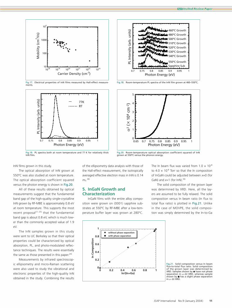
mobility of 1130 cm2/ Vs. The source of this
high-level residual carrier concentration, how-
ever, remains unclear.
The room-temperature PL spectra of a
250-nm-thick film grown with precisely con-
trolled temperatures, as described in §3.1,
are shown in Fig.18. Here, Ar+ laser at 514.5
nm with a power density of 2.2 W/ cm2 was
used as an excitation source. An InGaAs pho-
todetector with a cutoff wavelength of 2.05
µm was used. The wavelength of the PL peak
position did not show any noticeable change
even if the excitation power was changed
over two orders of magnitude from 65 mW/
cm2 to 6.5 W/ cm2.
The PL spectra at room temperature
and 77 K observed for 1.5-µm-thick InN are
shown in Fig.19. Very strong and sharp lu-
minescence was observed at 77 K with an
FWHM of 24 meV. The FWHM at room tem-
perature was 38 meV. This PL should origi-
nate from the fundamental interband transi-
tion of the InN film. No PL corresponding to
1.9 eV transition could be observed from any
1018
1019
1020
100
1000
104
0 500 1000 1500 2000
Carrier Density
Mobility
Car
rier
Den
sity
(cm
-3)
Mo
bili
ty (
cm2 /V
s)
Film Thickness (nm)
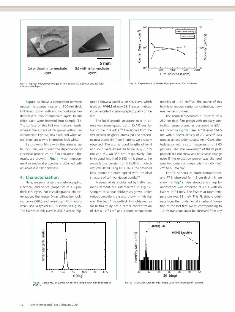
Figure 13 shows a comparison between
optical microscope images of 600-nm thick
InN layers grown with and without interme-
diate layers. Two intermediate layers 10 nm
thick each were inserted into sample (B).
The surface of this InN was mirror-smooth,
whereas the surface of InN grown without an
intermediate layer (A) has black and white ar-
eas. Here, areas with In droplets look white.
By growing films with thicknesses up
to 1500 nm, we studied the dependence of
electrical properties on film thickness. The
results are shown in Fig.14. Much improve-
ment in electrical properties is obtained with
an increase in film thickness.
4. CharacterizationHere, we summarize the crystallographic,
electrical, and optical properties of 1.5-µm-
thick InN layers. For crystallographic charac-
terization, the ω -scan X-ray diffraction rock-
ing curve (XRC) and ω–2θ scan XRD results
were used. A typical XRC is shown in Fig.15.
The FWHM of this curve is 236.7 arcsec. Fig-
ure 16 shows a typical ω–2θ XRD curve, which
gives an FWHM of only 28.9 arcsec, indicat-
ing an excellent crystallographic quality of the
film.
The local atomic structure near In at-
oms was investigated using EXAFS oscilla-
tion of the In K edge.37) The signals from the
first-nearest neighbor atoms (N) and second-
nearest atoms (In) from In atoms were clearly
observed. The atomic bond lengths of In–N
and In–In were estimated to be dIn–N=0.215
nm and d In–In=0.353 nm, respectively. The
In–In bond length of 0.353 nm is close to the
a-axis lattice constant of 0.3536 nm, which
was calculated using XRD. Thus, the obtained
local atomic structure agreed with the ideal
structure of sp3 hybridation bonds.37)
A series of data obtained by Hall-effect
measurement are summarized in Fig.17.
Samples of various thicknesses grown under
various conditions are also shown in this fig-
ure. The best 1.5-µm-thick film obtained so
far in this study has a carrier concentration
of 4.9 × 1018 cm-3 and a room temperature
Fig.13. Optical microscopy images of InN grown (a) without and (b) with intermediate layers.
Fig.14. Dependence of electrical properties on fi lm thickness.
Fig.15. ω -scan XRC of (0002) InN for the sample with fi lm thickness of 1500 nm.
Fig.16. ω–2θ XRD curve for InN sample with fi lm thickness of 1500 nm.
(a) without intermediatelayer
(b) with intermediatelayers
5 mm
15 15.5 16 16.5 17 17.5(deg)θ
Inte
nsit
y (a
rb. u
nits
)
30
(0002) InN
(0006) Sapphire
32 34 36 38 40 42(deg)2θ
Inte
nsit
y (a
rb. u
nits
)
Part1 Invited Review PaperInvited Review Paper
JSAP International No.9 (January 2004) 11
0.7 0.75 0.8 0.85 0.9 0.95 1
Photon Energy (eV)
77KRT
PL In
tens
ity
(arb
. uni
ts)
InN films grown in this study.
The optical absorption of InN grown at
550ºC was also studied at room temperature.
The optical absorption coefficient squared
versus the photon energy is shown in Fig.20.
All of these results obtained by optical
measurements suggest that the fundamental
band gap of the high-quality single-crystalline
InN grown by RF-MBE is approximately 0.8 eV
at room temperature. This supports the most
recent proposal21–25) that the fundamental
band gap is about 0.8 eV, which is much low-
er than the commonly accepted value of 1.9
eV.
The InN samples grown in this study
were sent to UC Berkeley so that their optical
properties could be characterized by optical
absorption, PL, and photo-modulated reflec-
tance techniques. The results were essentially
the same as those presented in this paper.24)
Measurements by infrared spectroscop-
ic ellipsometry and micro-Raman scattering
were also used to study the vibrational and
electronic properties of the high-quality InN
obtained in the study. Combining the results
of the ellipsometry data analysis with those of
the Hall-effect measurement, the isotropically
averaged effective electron mass in InN is 0.14
m0.38)
5. InGaN Growth and Characterization
InGaN films with the entire alloy compo-
sition were grown on (0001) sapphire sub-
strates at 550ºC by RF-MBE after a low-tem-
perature buffer layer was grown at 280ºC.
10
100
1000
104
1018 1019 1020 1021 1022 1023
Mo
bili
ty (
cm2 /V
s)
Carrier Density (cm-3)
Fig.17. Electrical properties of InN fi lms measured by Hall-effect measure-ments.
Fig.18. Room-temperature PL spectra of the InN fi lm grown at 460–550ºC.
Fig.19. PL spectra both at room temperature and 77 K for relatively thick InN fi lm.
Fig.20. Room-temperature optical absorption coeffi cient squared of InN grown at 550ºC versus the phonon energy.
The In beam flux was varied from 1.0 × 10⁻⁸
to 4.0 × 10⁻⁸ Torr so that the In composition
of InGaN could be adjusted between x=0 (for
GaN) and x=1 (for InN).39)
The solid composition of the grown layer
was determined by XRD. Here, all the lay-
ers are assumed to be fully relaxed. The solid
composition versus In beam ratio (In flux to
total flux ratio) is plotted in Fig.21. Unlike
in the case of MOVPE, the solid composi-
tion was simply determined by the In-to-Ga
0.7 0.75 0.8 0.85 0.9 0.95 1
Photon Energy (eV)
460ºC Growth
480ºC Growth
500ºC Growth
510ºC Growth
520ºC Growth
530ºC Growth
540ºC Growth
550ºC GrowthSapphire Sub
PL In
tens
ity
(arb
. uni
ts)
0.650
1
2
3
4
5
0.7 0.75 0.8 0.85 0.9 0.95 1Photon Energy (eV)
α2 (
10
8 c
m-2
)
0
0.2
0.4
0.6
0.8
1
0 0.2 0.4 0.6 0.8 1
without phase separation
with phase separation
In C
om
po
siti
on
In/(In+Ga)
Fig.21. Solid composition versus In beam fl ux-to-total fl ux ratio. Solid composition of the grown layer was determined by XRD. Samples shown by � have not phase separation in ω–2θ XRD, whereas sample shown by � has a slight phase separation in ω–2θ XRD.

12 JSAP International No.9 (January 2004)
GaN over the entire alloy
composition range.
Figures 23 and 24
show the CL and PL spec-
tra obtained at liquid-nitro-
gen temperature, respec-
tively. CL and PL emissions
were observed for all sam-
ples, confirming their good
crystalline quality.
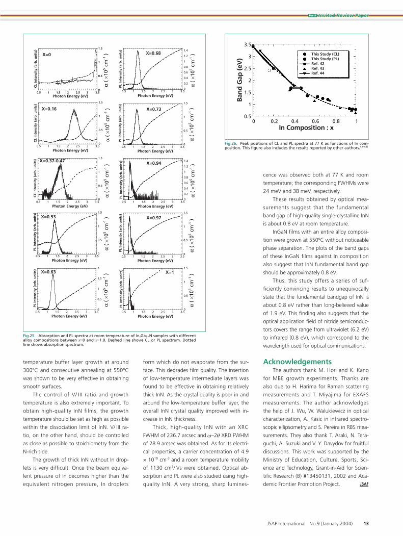
Figure 25 shows the
absorption and PL spectra of 10 samples
with different alloy compositions ranging
between x=0 and x=1.0. The luminescence
peak position and absorption edge roughly
agree for all the samples over the entire al-
loy composition range. Figure 26 shows
peak energies obtained from the CL and PL
spectra as functions of In composition. This
figure also includes the results reported by
other authors.42–44) The plots of the lumines-
cence peak positions in Fig.26 can be fit to
a smooth curve Eg=3.48-2.70x-bx(1-x) with
a bowing parameter b=2.3 eV.39) Here, the
Moss–Burstein effect is not taken into ac-
count.
These results on the optical properties of
InGaN over the entire alloy composition range
are consistent with the InN bandgap energy
of about 0.8 eV.
6. ConclusionsRecent developments in growth and
characterization of InN and related alloys are
reviewed. InN and InGaN growth on (0001)
sapphire was studied by RF-plasma-excited
molecular beam epitaxy. In this growth meth-
od, neutral and ionized, excited nitrogen at-
oms and molecules are generated using a
plasma source. Thus, the crystal growth tem-
perature can be set independent of the re-
quirements for pyrolysis of a nitrogen source.
This enabled us to grow InN at a relatively
low temperature without noticeable dissocia-
tion of the InN surface.
It was shown that nitridation of the sap-
phire substrates prior to growth is very effec-
tive for producing single crystals. It was also
suggested that an atomically flat surface is
essential for obtaining high-quality InN films.
The two-step growth method involving low-
flux ratio. A large difference between solid
composition and vapor phase composition
were reported when high-quality InGaN lay-
ers were grown at 800ºC by MOVPE.40) All
the InGaN layers with various solid composi-
tions grown at 550ºC in this study have suffi-
ciently good crystalline quality to emit strong
PL at 77 K, which will be shown later in this
section. The easy control of InGaN solid com-
position is another advantage of the RF-MBE
growth method.
Figure 22 shows the ω–2θ XRD curves
for InxGa1-xN (0<x<1). We confirmed that we
can successfully grow InxGa1-xN films over the
entire composition range (x=0.16, 0.37–0.47,
0.53, 0.63, 0.68, 0.73, 0.94, 0.97). Phase
separation did not occur in InxGa1-xN films
with x>0.53.39) This is probably due to the
relatively low growth temperature and the in-
sertion of an InN buffer layer.
Because of the slow atom migration at
low temperature, complete equilibrium might
not have occurred during growth. In addition,
the thermodynamical calculations by Kanga-
wa et al.41) showed that the mixing enthalpy
of InGaN is much smaller on an InN substrate
than on a GaN substrate. They reported that
the mixing enthalpy of InGaN became even
smaller than that of free-standing InGaN
when they were grown on InN. These effects
can probably explain why we could grow In-
x=0.53
x=0.37-0.47
x=0.63
x=0.16
x=0.97
x=0.94
x=0.73
x=0.68
31 32 33 34 35 31 32 33 34 35
2θ [deg] 2θ [deg]
Inte
nsi
ty (
arb
. un
its)
Inte
nsi
ty (
arb
. un
its)
Fig.22. ω–2θ XRD curves for InxGa1-xN (x=0.16, 0.37–0.47, 0.53, 0.63, 0.68, 0.73, 0.94, 0.97).
300 400 500 600 700 800Wavelength (nm)
X=0
X=0.16
X=0.37-0.47
Inte
nsi
ty (
arb
. un
its)
Fig.23. CL spectra at 77 K for the InxGa1-xN samples (x=0, 0.16, 0.37–0.47).
600 800 1000 1200 1400 1600Wavelength (nm)
X=0.37-0.47
X=0.53
X=0.63
X=0.68
X=0.73
X=0.94X=0.98
X=1
Inte
nsi
ty (
arb
. un
its)
Fig.24. PL spectra at 77 K for the InxGa1-xN samples (x=0.37–0.47, 0.53, 0.63, 0.68, 0.73, 0.94, 0.98, 1).
Part1 Invited Review PaperInvited Review Paper
JSAP International No.9 (January 2004) 13
temperature buffer layer growth at around
300ºC and consecutive annealing at 550ºC
was shown to be very effective in obtaining
smooth surfaces.
The control of V/ III ratio and growth
temperature is also extremely important. To
obtain high-quality InN films, the growth
temperature should be set as high as possible
within the dissociation limit of InN. V/ III ra-
tio, on the other hand, should be controlled
as close as possible to stoichiometry from the
N-rich side.
The growth of thick InN without In drop-
lets is very difficult. Once the beam equiva-
lent pressure of In becomes higher than the
equivalent nitrogen pressure, In droplets
αα (
×105 c
m-1
)
0.5 1 1.5 2 2.5 3 3.50
0.5
1
1.5
Photon Energy (eV)
α (
×105 c
m-1
)
0
0.5
1
1.5
0.5 1 1.5 2 2.5 3 3.5
Photon Energy (eV)
0
0.5
1
1.5
0.5 1 1.5 2 2.5 3 3.5
Photon Energy (eV)
α (
×105 c
m-1
)
0
0.5
1
1.5
0.5 1 1.5 2 2.5 3 3.5
Photon Energy (eV)
α (
×105 c
m-1
)
0
0.5
1
1.5
2
0.5 1 1.5 2 2.5 3 3.5
Photon Energy (eV)
α (
×105 c
m-1
)
0
0.2
0.4
0.6
0.8
1
1.2
1.4
0.5 1 1.5 2 2.5 3 3.5
Photon Energy (eV)
α (
×105 c
m-1
)
0
0.5
1
1.5
0.5 1 1.5 2 2.5 3 3.5
Photon Energy (eV)
α (
×105 c
m-1
)0
0.2
0.4
0.6
0.8
1
1.2
1.4
0.5 1 1.5 2 2.5 3 3.5
Photon Energy (eV)
α (
×105 c
m-1
)
0
0.5
1
1.5
0.5 1 1.5 2 2.5 3 3.5
Photon Energy (eV)
α (
×105 c
m-1
)
0
0.5
1
1.5
0.5 1 1.5 2 2.5 3 3.5
Photon Energy (eV)
α (
×105 c
m-1
)
X=0
X=0.16
X=0.37-0.47
X=0.53
X=0.63
X=0.68
X=0.73
X=0.94
X=0.97
X=1
CL
Inte
nsi
ty (
arb
. un
its)
PL In
ten
sity
(ar
b. u
nit
s)
CL
Inte
nsi
ty (
arb
. un
its)
PL In
ten
sity
(ar
b. u
nit
s)PL
Inte
nsi
ty (
arb
. un
its)
CL
Inte
nsi
ty (
arb
. un
its)
PL In
ten
sity
(ar
b. u
nit
s)
PL In
ten
sity
(ar
b. u
nit
s)
PL In
ten
sity
(ar
b. u
nit
s)
PL In
ten
sity
(ar
b. u
nit
s)
Fig.25. Absorption and PL spectra at room temperature of InxGa1-xN samples with different alloy compositions between x=0 and x=1.0. Dashed line shows CL or PL spectrum. Dotted line shows absorption spectrum.
Fig.26. Peak positions of CL and PL spectra at 77 K as functions of In com-position. This fi gure also includes the results reported by other authors.42–44)
0.5
1
3
1.5
2
2.5
3.5
0 0.2 0.4 0.6 0.8 1
This Study (CL)This Study (PL)Ref. 42Ref. 43Ref. 44
Band
Gap
(eV
)
In Composition : x
form which do not evaporate from the sur-
face. This degrades film quality. The insertion
of low-temperature intermediate layers was
found to be effective in obtaining relatively
thick InN. As the crystal quality is poor in and
around the low-temperature buffer layer, the
overall InN crystal quality improved with in-
crease in InN thickness.
Thick, high-quality InN with an XRC
FWHM of 236.7 arcsec and ω–2θ XRD FWHM
of 28.9 arcsec was obtained. As for its electri-
cal properties, a carrier concentration of 4.9
× 1018 cm-3 and a room temperature mobility
of 1130 cm2/ Vs were obtained. Optical ab-
sorption and PL were also studied using high-
quality InN. A very strong, sharp lumines-
cence was observed both at 77 K and room
temperature; the corresponding FWHMs were
24 meV and 38 meV, respectively.
These results obtained by optical mea-
surements suggest that the fundamental
band gap of high-quality single-crystalline InN
is about 0.8 eV at room temperature.
InGaN films with an entire alloy composi-
tion were grown at 550ºC without noticeable
phase separation. The plots of the band gaps
of these InGaN films against In composition
also suggest that InN fundamental band gap
should be approximately 0.8 eV.
Thus, this study offers a series of suf-
ficiently convincing results to unequivocally
state that the fundamental bandgap of InN is
about 0.8 eV rather than long-believed value
of 1.9 eV. This finding also suggests that the
optical application field of nitride semiconduc-
tors covers the range from ultraviolet (6.2 eV)
to infrared (0.8 eV), which correspond to the
wavelength used for optical communications.
AcknowledgementsThe authors thank M. Hori and K. Kano
for MBE growth experiments. Thanks are
also due to H. Harima for Raman scattering
measurements and T. Miyajima for EXAFS
measurements. The author acknowledges
the help of J. Wu, W. Walukiewicz in optical
characterization, A. Kasic in infrared spectro-
scopic ellipsometry and S. Pereira in RBS mea-
surements. They also thank T. Araki, N. Tera-
guchi, A. Suzuki and V. Y. Davydov for fruitful
discussions. This work was supported by the
Ministry of Education, Culture, Sports, Sci-
ence and Technology, Grant-in-Aid for Scien-
tific Research (B) #13450131, 2002 and Aca-
demic Frontier Promotion Project.

Part1 Invited Review PaperInvited Review Paper
14 JSAP International No.9 (January 2004)
Tomohiro Yamaguchi was born in Nagano Pre-fecture, Japan on March 1, 1978. He received his M.E. degree in Science and Engineering from Ritsumeikan University in 2001. He is currently working toward the Ph. D in the Department of Photonics, Ritsumeikan
University. His current research interests are the initial growth study and characterization of InN and related alloy semiconductors. He is a member of The Japan Society of Applied Physics, The Japanese Association for Crystal Growth and The Institute of Electronics, Information and Communication Engineers.
Yoshiki Saito was born in Hyogo Prefecture, Ja-pan on April 7, 1975. He received his B.E., M.E. and Ph. D. degrees in Science and Engineering from Rit-sumeikan University in 1998, 2000 and 2003, re-spectively. He is currently belonging to Faculty of Science and Engineering
of Ritsumeikan University. His current research inter-ests are growth and characterization of InN and re-lated alloy semiconductors by RF-Plasma-Excited Mo-lecular Beam Epitaxy. He is a member of The Japan Society of Applied Physics.
References
26 ) A. Wakahara and A. Yoshida: Appl. Phys. Lett. 54 (1989) 709.
27 ) T. Yamaguchi, Y. Saito, K. Kano, T. Araki, N. Teraguchi, A. Suzuki and Y. Nanishi: Proc. Int. Conf. Indium Phosphide and Related Materi-als, 2002, PII-41, p.643.
28 ) T. Yamaguchi, Y. Saito, K. Kano, T. Araki, N. Teraguchi, A. Suzuki and Y. Nanishi: Phys. Status Solidi B 228 (2001) 17.
29 ) T. Yamaguchi, T. Araki, Y. Saito, T. Maruyama, Y. Nanishi, N. Teraguchi and A. Suzuki: Inst. Phys. Conf. Ser. 170 (2002) 765.
30 ) A. Yamamoto, Y. Murakami, K. Koide, M. Adachi and A. Hashimoto: Phys. Status Solidi B 228 (2001) 5.
31 ) Y. Saito, N. Teraguchi, A. Suzuki, T. Araki and Y. Nanishi: Proc. Int. Workshop Nitride Semi-conductors (The Institute of Pure and Applied Physics, Tokyo, 2000) IPAP Conf. Series 1, p. 182.
32 ) S. V. Ivanov: Nitride Semiconductors (Hand book on Materials and Devices), eds. P. Ruter-ana, M. Albrecht and J. Neugebauor (Wiley-VCH, Berlin, 2002).
33 ) Y. Saito, N. Teraguchi, A. Suzuki, T. Yamagu-chi, T. Araki and Y. Nanishi: Mat. Res. Symp. Proc. 639 (2001) G11.18.
34 ) Y. Saito, Y. Tanabe, T. Yamaguchi, N. Teragu-chi, A. Suzuki, T. Araki and Y. Nanishi: Phys. Status Solidi B 228 (2001) 13.
35 ) M. Mayumi, F. Sato, Y. Kumagai, K. Takemo-to and A. Koukitsu: Phys. Status Solidi B 228 (2001) 537.
36 ) Y. Saito, T. Yamaguchi, H. Kanazawa, K. Kano, T. Araki, Y. Nanishi, N. Teraguchi and A. Suzuki: J. Cryst. Growth 237–239 (2002) 1017.
37 ) T. Miyajima, Y. Kudo, K. L. Liu, T. Uruga, T. Honma, Y. Saito, M. Hori, Y. Nanishi, T. Ko-bayashi and S. Hirata: Phys. Status Solidi B 234 (2002) 801.
38 ) A. Kasic, M. Schubert, Y. Saito, Y. Nanishi and G. Wagner: Phys. Rev. B 65 (2002) 115206.
39 ) M. Hori, K. Kano, T. Yamaguchi, Y. Saito, T. Araki, Y. Nanishi, N. Teraguchi and A. Suzuki: Phys. Status Solidi B 234 (2002) 750.
40 ) N. Yoshimoto, T. Matsuoka, T. Sasaki and A. Katsui: Appl. Phys. Lett. 59 (1991) 2251.
41 ) Y. Kangawa, T. Ito, A. Mori and A. Koukitsu: J. Cryst. Growth 220 (2000) 401.
42 ) C. Wetzel, T. Takeuchi, S. Yamaguchi, H. Ka-toh, H. Amano and I. Akasaki: Appl. Phys. Lett. 73 (1998) 1994.
43 ) V. Y. Davydov, A. A. Klochikhin, V. V. Emt-sev, S. V. Ivanov, V. V. Vekshin, F. Bechstedt, J. Furthmuller, H. Harima, A. V. Mudryi, A. Hashimoto, A. Yamamoto, J. Adrhold, J. Graul and E. E. Haller: Phys. Status Solidi B 230 (2002) R4.
44 ) K. P. O'Donnell, J. F. W. Mosselmans, R. W. Martin, S. Pereira and M. E. White: J. Phys.: Condens. Matter 13 (2001) 6977.
Yasushi Nanishi was born in Tokushima Pre-fecture, Japan in 1945. He received a B.E. degree from Nagoya Institute of Technology in 1969 and M.E. and Ph. D. degrees from Nagoya University in 1971 and 1986, respec-tively. From 1971 to 1994, he was a member of a
research staff at NTT LSI and Opto-electronics Labo-ratories, Atsugi, Japan. From 1978 to 1980, he was a visiting scientist at Massachusetts Institute of Tech-nology. Since 1994 he has been a professor in the Department of Photonics at Ritsumeikan University. He has been engaged in the research fields concern-ing GaAs MES FETs, Liquid Phase Epitaxy of GaAs, growth and characterization of bulk GaAs, correla-tion between GaAs crystal defects and FET perfor-mances and Plasma Excited Molecular Beam Epi-taxy. His latest interests are in MBE growth of Nitride Semiconductors and its application to both electronic and optoelectronic devices. He has been a leader of NEDO's regional consortium project and METI's na-tional project on high-power, high-frequency GaN electronic devices. He is a member of The Japan So-ciety of Applied Physics, The Institute of Electrical En-gineers of Japan, The Institute of Electronics, Infor-mation and Communication Engineers, The Japanese Association for Crystal Growth and American Mate-rial Research Society.
1 ) F. Fischer and F. Schröter: Ber. Dtsch. Keram Ges. 43 (1910) 1465.
2 ) J. B. MacChesney, P. M. Bridenbaugh and P. B. O'Connor: Mater. Res. Bull. 5 (1970) 783.
3 ) K. Osamura, S. Nara and Y. Murakami: J. Ap-pl. Phys. 46 (1975) 3432.
4 ) H. J. Hovel and J. J. Cuomo: Appl. Phys. Lett. 20 (1972) 71.
5 ) K. L. Westra, R. P. W. Lawson and M. J. Brett: J. Vac. Sci. Technol. A 6 (1988) 1730.
6 ) K. Osamura, K. Nakajima and Y. Murakami: Solid State Commun. 11 (1972) 617.
7 ) J. W. Trainor and K. Rose: J. Electron. Mater. 3 (1974) 821.
8 ) N. Puychevrier and M. Menoret: Thin Solid Films 36 (1976) 141.
9 ) V. A. Tyagai, A. M. Evstigneev, A. N. Krasiko, A. F. Andreeva and V. Y. Malakhov: Sov. Phys. Semicond. 11 (1977) 1257.
10 ) B. R. Natarajan, A. H. Eltoukhy and J. E. Greene: Thin Solid Films 69 (1980) 201.
11 ) H. Takeda and T. Hada: Toyama Kogyou Koto Semmon Gakko Kiyo 11 (1977) 73 (in Japa-nese).
12 ) T. L. Tansley and C. P. Foley: J. Appl. Phys. 59 (1986) 3241.
13 ) T. Matsuoka, H. Tanaka and A. Katsui: Int. Symp. on GaAs and Related Compounds, Karuizawa, Japan 1989, Inst. Phys. Conf. Ser. 106 (1990) p.141.
14 ) A. Yamamoto, T. Shinya, T. Sugiura and A. Hashimoto: J. Cryst. Growth 189 (1998) 461.
15 ) S. Yamaguchi, M. Kariya, S. Nitta, T. Takeuchi, C. Wetzel, H. Amano and I. Akasaki: J. Appl. Phys. 85 (1999) 7682.
16 ) A. Yamamoto, T. Tanaka, K. Koide and A. Hashimoto: Phys. Status Solidi B 194 (2002) 510.
17 ) W. E. Hoke, P. J. Lemonias and D. G. Weir: J. Cryst. Growth 111 (1991) 1024.
18 ) M. Higashiwaki and T. Matsui: Jpn. J. Appl. Phys. 41 (2002) L540.
19 ) H. Lu, W. J. Schaff, J. Hwang, H. Wu, G. Koley and L. F. Eastman: Appl. Phys. Lett. 79 (2001) 1489.
20 ) Y. Saito, N. Teraguchi, A. Suzuki, T. Araki and Y. Nanishi: Jpn. J. Appl. Phys. 40 (2001) L91.
21 ) T. Inushima, V. V. Mamutin, V. A. Vekshin, S. V. Ivanov, T. Sakon and S. Motokawa: J. Cryst. Growth 227 (2001) 481.
22 ) V. Y. Davydov, A. A. Klochikhin, R. P. Sei-syan, V. V. Emtsev, S. V. Ivanov, F. Bechstedt, J. Furthmuller, H. Harima, A. V. Mudryi, J. Adrhold, O. Semchinova and J. Graul: Phys. Status Solidi B 229 (2002) R1.
23 ) T. Matsuoka, H. Okamoto, M. Nakao, H. Harima and E. Kurimoto: Appl. Phys. Lett. 81 (2002) 1246.
24 ) J. Wu, W. Walukiewicz, K. M. Yu, J. W. Arger, III, E. E. Haller, H. Lu, W. J. Schaff, Y. Saito and Y. Nanishi: Appl. Phys. Lett. 80 (2002) 3967.
25 ) Y. Saito, H. Harima, E. Kurimoto, T. Yamagu-chi, N. Teraguchi, A. Suzuki, T. Araki and Y. Nanishi: Phys. Status Solidi B 234 (2002) 796.