lab 1 - digital logic - binary numbers+ basic logic operations
TRANSCRIPT

8/8/2019 Lab 1 - Digital Logic - Binary Numbers+ Basic Logic Operations
http://slidepdf.com/reader/full/lab-1-digital-logic-binary-numbers-basic-logic-operations 1/17
Youri Abou-Samra - HCU July 5, 2010
Page 1 of 17
Lab 1 - Digital Logic - Binary Numbers+ Basic Logic Operations
Introduction - Why Do You Want to Learn This Material?
In this lesson you're going to be introduced to Digital Logic. There are lots of reasons tolearn digital logic. Here are some of those reasons.
• Digital logic is the foundation for digital computers. If you want to understand theinnards of computers you need to know digital logic.
• Digital logic has relations to other kinds of logic including:
o Formal logic - as taught by many philosophy departmentso Fuzzy logic - a tool used to design control systems and many other systems.
o So, in learning digital logic you learn something that helps you elsewhere.
• For many students, learning digital logic is fun.
What Are You Going to Learn?
There are at least two general areas you need to become familiar with.
• First, there's background you need to know - the basics of digital logic - things like zerosand ones (0s and 1s) and how you can represent signals as sequences of zeroes and ones.
Eventually you will want to know how large arrays of zeroes and ones can be used in
computer files to store information in pictures, documents, sounds and even movies and
you'll want to learn about how information can be transmitted, between computers and
digital signal sources.• You will also need to know things about digital circuits - gates, flip-flops and memory
elements and others - so that you can eventually design circuits to manipulate digitalsignals.
Here is a short list of the topics you will learn.
• Learn what logic signals look like
• Model logic signals
• Learn Boolean algebra for logic analysis
• Learn about gates that process logic signals
• Learn how to design some smaller logic circuits• Learn about flip-flops and memory elements that store logic signals

8/8/2019 Lab 1 - Digital Logic - Binary Numbers+ Basic Logic Operations
http://slidepdf.com/reader/full/lab-1-digital-logic-binary-numbers-basic-logic-operations 2/17
Youri Abou-Samra - HCU July 5, 2010
Page 2 of 17
Objectives for This Lesson
Here's what we are after in this lesson - what you should be able to do.
• Given a system that uses logic signals
o Be able to specify what the output will be when the input is zero (0) and what theoutput will be when the input is one (1).
• Given an AND, OR, NAND or NOT gate,
o Be able to determine the output of the gate given the input logic signals.
• Given a system that requires gates,o Be able to wire a chip correctly, and to check that the chip is functioning properly.
Logic Signals
There are a number of different systems for representing binary information in physicalsystems. Here are a few.
• A voltage signal with zero (0) corresponding to 0 volts and one (1) corresponding to five
or three volts.
• A sinusoidal signal with zero corresponding to some frequency, and one corresponding tosome other frequency.
• A current signal with zero corresponding to 4 milliamps and one corresponding to 20
milliamps.
• And one last way is to use switches, OPEN for "0" and CLOSED for "1".
• (And there are more ways!)
Characteristics of Logic Signals
We should note that all of these signals can and usually will change in time, so that wereally are looking at dynamic situations. However, we will start by looking at these signals asthough they were not changing in time.
• We will pick a voltage signal as a working example. It can take on two valuescorresponding to 0 and 1.
• We can associate a variable with that logic signal, and we can assign a symbol to
represent that variable - like the symbol A.

8/8/2019 Lab 1 - Digital Logic - Binary Numbers+ Basic Logic Operations
http://slidepdf.com/reader/full/lab-1-digital-logic-binary-numbers-basic-logic-operations 3/17
Youri Abou-Samra - HCU July 5, 2010
Page 3 of 17
Think Binary!
Let's examine a typical situation. You have some sort of device that generates a logicsignal.
• It could be a telephone that converts your voice signal into a sequence of zeros and ones.• It could be the thermostat on the wall that generates a 1 when the temperature is too low,
and a 0 when the temperature is above the set point temperature.
The logic signal, A, takes on values of 0 (FALSE, OFF) or 1 (TRUE, ON). That signal
might really be a voltage, a switch closure, etc. However, we want to think in terms of zeros and
ones, not in terms of the values of the voltage.
Operations on Logic Signals
Once we have the concept of a logic signal we can talk about operations that can beperformed on logic signals. Begin by assuming we have two logic signals, A and B. Then
assume that those two signals form an input set to some circuit that takes two logic signals as
inputs, and has an output that is also a logic signal. That situation is represented below.
The output, C, depends upon the inputs, A and B. There are many different ways that C
could depend upon A and B. The output, C, is a function, - a logic function - of the inputs, A
and B. We will examine a few basic logic functions - AND, OR and NOT functions and start
learning the circuitry that you use to implement those functions.

8/8/2019 Lab 1 - Digital Logic - Binary Numbers+ Basic Logic Operations
http://slidepdf.com/reader/full/lab-1-digital-logic-binary-numbers-basic-logic-operations 4/17
Youri Abou-Samra - HCU July 5, 2010
Page 4 of 17
Logic Gates
If we think of two signals, A and B, as representing a truth value of two different propositions,
then A could be either TRUE (a logical 1) or FALSE (a logical 0). B can take on the same
values. Now consider a situation in which the output, C, is TRUE only when both A is TRUE
and B is TRUE. We can construct a truth table for this situation. In that truth table, we insert all
of the possible combinations of inputs, A and B, and for every combination of A and B we list
the output, C.
AND Gate
A B C
False False False
False True False
True False False
True True True
Table 1.1: An AND Example
8/8/2019 Lab 1 - Digital Logic - Binary Numbers+ Basic Logic Operations
http://slidepdf.com/reader/full/lab-1-digital-logic-binary-numbers-basic-logic-operations 5/17
Youri Abou-Samra - HCU July 5, 2010
Page 5 of 17
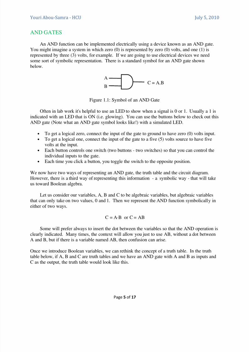
AND GATES
An AND function can be implemented electrically using a device known as an AND gate.You might imagine a system in which zero (0) is represented by zero (0) volts, and one (1) is
represented by three (3) volts, for example. If we are going to use electrical devices we need
some sort of symbolic representation. There is a standard symbol for an AND gate shownbelow.
Figure 1.1: Symbol of an AND Gate
Often in lab work it's helpful to use an LED to show when a signal is 0 or 1. Usually a 1 is
indicated with an LED that is ON (i.e. glowing). You can use the buttons below to check out this
AND gate (Note what an AND gate symbol looks like!) with a simulated LED.
• To get a logical zero, connect the input of the gate to ground to have zero (0) volts input.
• To get a logical one, connect the input of the gate to a five (5) volts source to have fivevolts at the input.
• Each button controls one switch (two buttons - two switches) so that you can control the
individual inputs to the gate.
• Each time you click a button, you toggle the switch to the opposite position.
We now have two ways of representing an AND gate, the truth table and the circuit diagram.However, there is a third way of representing this information - a symbolic way - that will take
us toward Boolean algebra.
Let us consider our variables, A, B and C to be algebraic variables, but algebraic variables
that can only take on two values, 0 and 1. Then we represent the AND function symbolically in
either of two ways.
C = A·B or C = AB
Some will prefer always to insert the dot between the variables so that the AND operation is
clearly indicated. Many times, the context will allow you just to use AB, without a dot betweenA and B, but if there is a variable named AB, then confusion can arise.
Once we introduce Boolean variables, we can rethink the concept of a truth table. In the truthtable below, if A, B and C are truth tables and we have an AND gate with A and B as inputs and
C as the output, the truth table would look like this.
A
BC = A.B

8/8/2019 Lab 1 - Digital Logic - Binary Numbers+ Basic Logic Operations
http://slidepdf.com/reader/full/lab-1-digital-logic-binary-numbers-basic-logic-operations 6/17
Youri Abou-Samra - HCU July 5, 2010
Page 6 of 17
AND Gate
A (Input) B (Input) C (Output)
0 0 0
0 1 0
1 0 0
1 1 1
Table 1.2: AND Gate Truth Table
Figure 1.2: AND GATE (7408)

8/8/2019 Lab 1 - Digital Logic - Binary Numbers+ Basic Logic Operations
http://slidepdf.com/reader/full/lab-1-digital-logic-binary-numbers-basic-logic-operations 7/17
Youri Abou-Samra - HCU July 5, 2010
Page 7 of 17
OR GATES
Consider a case where a pressure can be high and a temperature can be high. Let's assume
we have two sensors that measure temperature and pressure. The first sensor has an output, T,which is 1 when a temperature in a boiler is too high and 0 otherwise. The second sensor
produces an output, P, which is 1 when the pressure is too high and 0 otherwise. Now, for theboiler, we have a dangerous situation when either the temperature or the pressure is too high. It
only takes one. Let's construct a truth table for this situation. The output, D, is 1 when dangerexists.
We represent the OR function symbolically as: C = A+B
OR Gate
A B C
False False False
False True True
True False True
True True True
Table 1.3: OR Gate Truth Table
What we have done is defined an OR gate. An OR gate is a gate for which the output is 1whenever one or more of the inputs is 1. The output of an OR gate is 0 only when all inputs are
0. Shown below is a schematic symbol for an OR gate, together with the simulated LEDs and
input buttons so that you can explore OR gate behavior.
In terms of Boolean variables, the truth table for an OR gate looks like this.
OR Gate
A (Input) B (Input) C (Output)
0 0 0
0 1 1
1 0 1
1 1 1
Table 1.4: OR Gate Truth Table
There is a standard symbol for an OR gate shown below.
Figure 1.3: OR GATE
A
BC = A+B

8/8/2019 Lab 1 - Digital Logic - Binary Numbers+ Basic Logic Operations
http://slidepdf.com/reader/full/lab-1-digital-logic-binary-numbers-basic-logic-operations 8/17
Youri Abou-Samra - HCU July 5, 2010
Page 8 of 17
Figure 1.4: OR GATE (7432)
NOT GATES (Inverters)
A third important logical element is the inverter. An inverter does pretty much what itsays. If the input is 0, the output is 1. Conversely, if the input is 1, the output is 0. The symbol
for an inverter is shown below. Again, you can putter with this inverter with the simulated
LEDs. X is the input to the inverter. The output is NOT-X represented as : X
Figure 1.5: NOT Gate
The truth table for an inverter is pretty simple since there is only one input. Call the input A, and
the output C, and the truth table is:
NOT GateA (Input) C (Output)
0 1
1 0
Table 1.5: NOT Gate Truth Table
A C = A

8/8/2019 Lab 1 - Digital Logic - Binary Numbers+ Basic Logic Operations
http://slidepdf.com/reader/full/lab-1-digital-logic-binary-numbers-basic-logic-operations 9/17
Youri Abou-Samra - HCU July 5, 2010
Page 9 of 17
Figure 1.6: NOT GATE (7404)
NAND Gates
There is another important kind of gate, the NAND gate. Actually, the way to start thinkingabout a NAND gate is to think of it as an AND gate with an inverter on the output. That's shown
below.
Figure 1.7: NAND Gate
Actually, however, the symbol for a NAND gate compresses the inverter down to a dot at the
output of the AND gate as shown below.
Figure 1.8: NAND Gate
A
BC = AB

8/8/2019 Lab 1 - Digital Logic - Binary Numbers+ Basic Logic Operations
http://slidepdf.com/reader/full/lab-1-digital-logic-binary-numbers-basic-logic-operations 10/17
Youri Abou-Samra - HCU July 5, 2010
Page 10 of 17
NAND Gate
A (Input) B (Input) C (Output)
0 0 1
0 1 1
1 0 1
1 1 0
Table 1.6: NAND Gate Truth Table
Figure 1.9: NAND GATE (7400LS)
See Appendix A for instruction on how to wire a Quad NAND Chip.

8/8/2019 Lab 1 - Digital Logic - Binary Numbers+ Basic Logic Operations
http://slidepdf.com/reader/full/lab-1-digital-logic-binary-numbers-basic-logic-operations 11/17
Youri Abou-Samra - HCU July 5, 2010
Page 11 of 17
NOR Gates
The way to start thinking about a NOR gate is to think of it as an OR gate with an inverteron the output. That's shown below.
Figure 1.10: NOR Gate
Actually, however, the symbol for a NOR gate compresses the inverter down to a dot at the
output of the OR gate as shown below.
Figure 1.11: NOR Gate
NOR Gate
A (Input) B (Input) C (Output)
0 0 1
0 1 0
1 0 0
1 1 0
Table 1.7: NOR Gate Truth Table
Figure 1.11: NOR Gate 7402LS
A
BC = A B

8/8/2019 Lab 1 - Digital Logic - Binary Numbers+ Basic Logic Operations
http://slidepdf.com/reader/full/lab-1-digital-logic-binary-numbers-basic-logic-operations 12/17
Youri Abou-Samra - HCU July 5, 2010
Page 12 of 17
8/8/2019 Lab 1 - Digital Logic - Binary Numbers+ Basic Logic Operations
http://slidepdf.com/reader/full/lab-1-digital-logic-binary-numbers-basic-logic-operations 13/17
Youri Abou-Samra - HCU
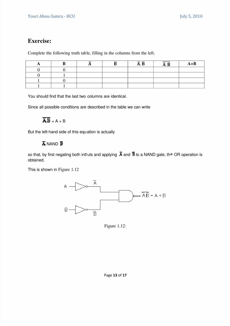
Exercise:
Complete the following truth tab
A B
0 0
0 1
1 0
1 1
You should find that the last two
Since all possible conditions are
= A + B
But the left-hand side of this equ
NAND
so that, by first negating both in
obtained.
This is shown in Figure 1.12
Page 13 of 17
le, filling in the columns from the left.
. .
columns are identical.
described in the table we can write
ation is actually
uts and applying and to a NAND gate, th
Figure 1.12:
July 5, 2010
A+B
OR operation is

8/8/2019 Lab 1 - Digital Logic - Binary Numbers+ Basic Logic Operations
http://slidepdf.com/reader/full/lab-1-digital-logic-binary-numbers-basic-logic-operations 14/17
Youri Abou-Samra - HCU July 5, 2010
Page 14 of 17
Appendix A
Wiring a Quad-NAND Chip
If you want to use gates, you will need to learn something about their physical
characteristics. In this section we'll walk you through wiring a simple gate circuit using one
specific integrated circuit (IC) the 7400 chip. It's a good introduction to some of the more
complex logic chips that you'll probably be using later.
Here's a picture of the 7400 chip in a circuit board. This chip is actually an N74LS00P.
The LS tells you that it is a low power Schottky chip. Every manufacturer will embed the 7400or 74LS00 in other part numbers.
Notice that this chip has fourteen pins.
If you want to use an IC chip, then you will always need to know the pinout. That'selectrical engineering lingo for describing the way the pins are connected to the internal circuitry
of the chip. You need to know where the power supply is connected and where the gate inputs
and outputs are connected. Here's the pinout for a 7400 chip.

8/8/2019 Lab 1 - Digital Logic - Binary Numbers+ Basic Logic Operations
http://slidepdf.com/reader/full/lab-1-digital-logic-binary-numbers-basic-logic-operations 15/17
Youri Abou-Samra - HCU July 5, 2010
Page 15 of 17
The first step in wiring the 7400 is to connect the positive power supply. Use a five volt
(5v) power supply and don't turn it on yet. Connect a lead to pin 14 as shown below, and
connect the other end of that lead to a 5v supply. Keep the power supply turned off until youhave everything connected. Here's what that looks like when the positive supply voltage to the
chip is wired.
The next step in wiring the 7400 is to connect the ground connection. Connect a lead to pin
7 as shown below, and connect the other end of that lead to ground.

8/8/2019 Lab 1 - Digital Logic - Binary Numbers+ Basic Logic Operations
http://slidepdf.com/reader/full/lab-1-digital-logic-binary-numbers-basic-logic-operations 16/17
Youri Abou-Samra - HCU July 5, 2010
Page 16 of 17
Notice the pattern to this connection. The power to this digital logic chip goes to thecorners. Remember, power to the corners for logic chips.
Now you can connect the two inputs to one of the gates on the chip. You're going to put 5von either of these inputs for a 1 and ground the input for a 0. There are two wires in the picture
below that connect to pins 1 and 2 on the chip. Those pins are the inputs for one of the NAND
gates on the chip.
Now you can connect the output of the gate. You will need to connect this output to
something like a voltmeter or an oscilloscope so that you can measure and observe the output of
the gate. (And the voltmeter or oscilloscope will also have to be connected to the ground. Youwill measure output voltage with respect to ground.) The output will be near 5v when the output
is a 1 and near 0v when the output is a 0.

8/8/2019 Lab 1 - Digital Logic - Binary Numbers+ Basic Logic Operations
http://slidepdf.com/reader/full/lab-1-digital-logic-binary-numbers-basic-logic-operations 17/17
Youri Abou-Samra - HCU July 5, 2010
Page 17 of 17
Actually, you can often connect LEDs to give a visual indication of a 1 (LED lighted) or a 0(LED dark). Here some LEDs are shown, together with 1k current limiting resistors. If you
connect LED indicators to your circuit remember that an LED is not the same in both directions,and you have to get the correct end connected to the resistor. The other end of each LED is
connected to ground (or just "grounded"). Here's the circuit to show the output of a NAND gate:
When the output of the gate is a 1, the output voltage will be five (5) volts. Current will flow
through the series combination of the resistor and the LED, so the LED will light. When the
output of the gate is a 0, the output voltage will be zero (0) volts and the LED will not be lit.Thus, the LED lights up when the output is a 1, and doesn't light when the output is a 0. You can
use this indication scheme to show the status for any signal. (It doesn't have to be the output of a
gate.)