lecture 03 overview of micro fabrication
TRANSCRIPT

Dr. S.Meenatchi Sundaram, Department of Instrumentation & Control Engineering, MIT, Manipal
ICE 4010: MICRO ELECTRO MECHANICAL SYSTEMS (MEMS)
Lecture #03
Silicon & Crystal Growth
Dr. S. Meenatchi Sundaram
Email: [email protected]
1

MEMS Materials and Their Preparation
2Dr. S.Meenatchi Sundaram, Department of Instrumentation & Control Engineering, MIT, Manipal
• Atoms within a mineral are arranged in an ordered geometricpattern which determine its "crystal structure".
• A crystal structure will determine as its symmetry, opticalproperties, cleavage and geometric shape.
• The recipe or mixture of these compounds becomes theblueprint for how the crystal will grow. This growth pattern iscalled as crystal's “habit”.
• The "unit cell" is the smallest divisible unit of a mineral withsymmetrical characteristics unique to a crystalline structure.
• A structure's "unit cell" is a spatial arrangement of atomswhich is tiled in three-dimensional space to form the crystal.
• The unit cell is determined by its lattice parameters, the lengthof the cell edges and the angles between them, while thepositions of the atoms inside the unit cell are described by theset of atomic positions (xi,yi,zi) measured from a lattice point.
Crystal Structures
3Dr. S.Meenatchi Sundaram, Department of Instrumentation & Control Engineering, MIT, Manipal

• The crystal system is a grouping of crystal structures thatare categorized according to the axial system used todescribe their "lattice".
• The seven unique crystal systems, listed in order ofdecreasing symmetry, are: 1. Isometric System, 2.Hexagonal System, 3. Tetragonal System, 4. Rhombohedric(Trigonal) System, 5. Orthorhombic System, 6. MonoclinicSystem, 7. Triclinic System.
Crystal System
4Dr. S.Meenatchi Sundaram, Department of Instrumentation & Control Engineering, MIT, Manipal
Why Silicon?
5Dr. S.Meenatchi Sundaram, Department of Instrumentation & Control Engineering, MIT, Manipal
• Most abundant material on earth.
• Mechanically stable and can be integrated into electronics.
• Same Young’s modulus as steel (2 x 10⁵ MPa) but as light asaluminum (2.3 g/cm3).
• Melting point at 1400 0C, which is about twice as high as that ofaluminum.
• Thermal coefficient is about 8 times smaller than that of steeland more than 10 times smaller than that of aluminum.
• Virtually no mechanical hysteresis.
• Silicon wafers are extremely flat and accept coatings andadditional thin-film layers.
• Greater flexibility in design and manufacture.
• Treatments and fabrication processes for silicon substrates arewell established and documented.

Doping
6Dr. S.Meenatchi Sundaram, Department of Instrumentation & Control Engineering, MIT, Manipal
• All Group V atoms will donate electrons if they substitute for hostatoms in crystals of Group IV elemental semiconductors (n-typesemiconductor ) where as Group III atoms will generate a hole (p-typesemiconductor ).

� Basically, the technique used for silicon crystal growth fromthe melt is the Czochralski technique.
� The technique starts when a pure form of sand (SiO2) calledquartzite is placed in a furnace with different carbon-releasingmaterials such as coal and coke. Several reactions take placeinside the furnace and the net reaction that results in silicon is
SiC + SiO2 ----> Si + SiO (gas) + CO (gas)
� The silicon so produced is called metallurgical-grade silicon(MGS), which contains up to 2 percent impurities.Subsequently, the silicon is treated with hydrogen chloride(HCl) to form trichlorosilane (SiHCl3):
Si + 3HCl ----> SiHCl3 (gas) + H2 (gas)
Silicon Crystal Growth from the Melt
7Dr. S.Meenatchi Sundaram, Department of Instrumentation & Control Engineering, MIT, Manipal

� SiHCl3 is liquid at room temperature. Fractionaldistillation of the SiHCl3 liquid removes impurities, andthe purified liquid is reduced in a hydrogen atmosphere toyield electronic grade silicon (EGS) through the reaction
SiHCl3 + H2 ----> Si + 3HCl
� EGS is a polycrystalline material of remarkably highpurity and is used as the raw material for preparing high-quality silicon wafers.
Silicon Crystal Growth from the Melt
8Dr. S.Meenatchi Sundaram, Department of Instrumentation & Control Engineering, MIT, Manipal
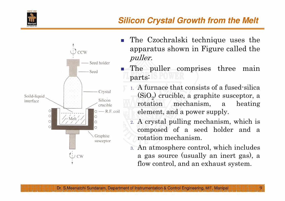
� The Czochralski technique uses theapparatus shown in Figure called thepuller.
� The puller comprises three mainparts:
1. A furnace that consists of a fused-silica(SiO2) crucible, a graphite susceptor, arotation mechanism, a heatingelement, and a power supply.
2. A crystal pulling mechanism, which iscomposed of a seed holder and arotation mechanism.
3. An atmosphere control, which includesa gas source (usually an inert gas), aflow control, and an exhaust system.
Silicon Crystal Growth from the Melt
9Dr. S.Meenatchi Sundaram, Department of Instrumentation & Control Engineering, MIT, Manipal

� In crystal growing, the EGS is placed in the crucible and thefurnace is heated above the melting temperature of silicon.
� An appropriately oriented seed crystal (e.g. [100]) issuspended over the crucible in a seed holder.
� The seed is lowered into the melt.
� Part of it melts but the tip of the remaining seed crystal stilltouches the liquid surface.
� The seed is then gently withdrawn.
� Progressive freezing at the solid-liquid interface yields a largesingle crystal.
� A typical pull rate is a few millimeters per minute.
� After a crystal is grown, the seed and the other end of theingot, which is last to solidify, are removed.
� Next, the surface is ground so that the diameter of thematerial is defined.
Silicon Crystal Growth from the Melt
10Dr. S.Meenatchi Sundaram, Department of Instrumentation & Control Engineering, MIT, Manipal
� After that, one or more flat regions are ground along thelength of the ingot.
� These flat regions mark the specific crystal orientationof the ingot and the conductivity type of the material.
� Finally, the ingot is sliced by a diamond saw into wafers.
� Slicing determines four wafer parameters: surfaceorientation, thickness, taper (which is the variation inthe wafer thickness from one end to another), and bow(i.e. surface curvature of the wafer, measured from thecentre of the wafer to its edge).
� Typical diameter of silicon wafers are 100mm, 150mm,200mm.
Silicon Crystal Growth from the Melt
11Dr. S.Meenatchi Sundaram, Department of Instrumentation & Control Engineering, MIT, Manipal

Silicon Crystal Growth from the Melt
12Dr. S.Meenatchi Sundaram, Department of Instrumentation & Control Engineering, MIT, Manipal

Silicon Crystal Growth from the Melt
13Dr. S.Meenatchi Sundaram, Department of Instrumentation & Control Engineering, MIT, Manipal