m156b30-40-239-0201 v0 250-280nit 窄边n80
TRANSCRIPT

1
安徽赛迈特光电股份安徽赛迈特光电股份有限公司有限公司
APPROVAL SHEET承 认 书
客户名称Customer
产品型号Part NO. M156B30-54-239-0201产品内容
Product typeMode: TFT LCD Module
备注栏Remarks
□APPROVAL FOR SEPCIFICATIONS ONLY■APPROVAL FOR SEPCIFICATIONS AND SAMPLE
客户确认签章Signature by Customer:
备注/ Notes:
PREPARED BY CHECKED BY APPROVED BY
安微省太湖县香熙镇观音路赛迈特工业园

2
安徽赛迈特光电股份安徽赛迈特光电股份有限公司有限公司
RECORDS OF REVISION
DATE NO REVISED No. PAGE SUMMARY NOTE
2020-08-20 Rev01 20 -

3
安徽赛迈特光电股份安徽赛迈特光电股份有限公司有限公司
1. ApplicationThis specification applies to a color TFT-LCM Module,
2. OverviewThis TFT-LCM Module is a color active matrix TFT LCD using amorphous silicon TFT's
(Thin Film Transistors) as an active switching devices. This FOB has a 15.6 inch diagonallymeasured active area with FHD resolutions (1920 horizontal by 1080vertical pixel array). Eachpixel is divided into RED, GREEN, BLUE dots which are arranged in vertical Stripe and this LCMcan display 16.7Mcolors. The TFT-LCD panel used for this FOB is a low reflection and highercolor type . All input signals are eDP1.2 interface compatible.
● 2 lane eDP Interface with 2.7Gbps Link Rates● Thin and light weight● 8-bit color depth, display 16.7M colors● Single LED Lighting Bar. (Down side/Horizontal Direction)● Green Product (RoHS & Halogen free product)● On board LED Driving circuit● Low driving voltage and low power consumption● On board EDID chip
3.Mechanical specifications.Parameter Specification Unit Note
Display size 15.6” (Diagonal) inch
Active area 344.16(H) ×193.59(V) mm
Pixel Format1920(H) ×1080(V)
(1pixel = R + G + B dot)pixel
Pixel pitch 0.17925(H) x 0.17925 (V) mm
Pixel configuration R, G, B vertical stripe
Display mode Normally black
Display colors 16.7M colors
Power Consumption 0.7 W
Surface treatment of frontpolarizer
Anti-glare coating: (3H)
Outline dimensionsParameter Min Typ Max Unit Remark
Unit outline dimensions
Width 350.46 350.76 351.06 mm
Height 204.66 204.96 205.26 mm
Depth 2.7 2.9 3.1 mm w/o PWB.[Note3-2]
Mass - - - g

4
安徽赛迈特光电股份安徽赛迈特光电股份有限公司有限公司
4. Input Terminals4-1 Driving interface of PWB
The electronics interface connector is UJU IS050-L30B-C10 or Compatible.The connector interface pin assignments are listed in Table 6.
<Table 6. Pin Assignments for the Interface Connector>
Pin No. Symbol I/O Function Remark
1 NC I NC
2 H_GND P High Speed round
3 Lane1_N I Complement Signal Link Lane 1
4 Lane1_P I True Signal Link Lane 1
5 H_GND P High Speed round
6 Lane0_N I Complement Signal Link Lane 0
7 Lane0_P I True Signal Link Lane 0
8 H_GND P High Speed round
9 AUX_CH_P I True Signal Auxiliary Channel
10 AUX_CH_N I Complement Signal Auxiliary Channel
11 H_GND P High Speed round
12 LCD_VDD P LCD logic and driver power(3.3V)
13 LCD_VDD P LCD logic and driver power(3.3V)
14 NC I NC
15 LCD_GND P LCD logic and driver ground
16 LCD_GND P LCD logic and driver ground
17 HPD O HPD signal pin
18 LED-1 P Backlight ground
19 LED-2 P Backlight ground
20 LED-3 P Backlight ground
21 LED-4 P Backlight ground
22 BL_ENABLE I Backlight on/off
23 BL_PWM_DIM I System PWM
24 NC - Reserved for LCD manufacturer’s use
25 NC - Reserved for LCD manufacturer’s use
26 BL_PWR P LED Power Supply 5V-21V;If not use,NC
27 BL_PWR P LED Power Supply 5V-21V;If not use,NC
28 BL_PWR P LED Power Supply 5V-21V;If not use,NC
29 BL_PWR P LED Power Supply 5V-21V;If not use,NC
30 NC Color Engin Function Reserved
*1 P: POWER I: Input O: OutputThe electronics interface connector is UJU IS050-L30B-C10 or Compatible.
Mating housing/ Part Number:I-PEX 20454-030T or CompatibleThe connector interface pin assignments are listed in Table 6.

5
安徽赛迈特光电股份安徽赛迈特光电股份有限公司有限公司
4-2 eDP interface
Lane 0 Lane 1R0-7:0 R1-7:0G0-7:0 G1-7:0B0-7:0 B1-7:0R2-7:0 R3-7:0G2-7:0 G3-7:0B2-7:0 B3-7:0R4-7:0 R5-7:0G4-7:0 G5-7:0B4-7:0 B5-7:0
Fig.4-2-4 eDP 2lane 6bit input data mapping
6
安徽赛迈特光电股份安徽赛迈特光电股份有限公司有限公司5. Electrical Characteristics
5-1 Absolute Maximum Ratings
Parameter Symbol ConditionRatings
Unit RemarkMIN MAX
+3.3V supply voltage VDD Ta=25℃ -0.3 +4.0 V
Backlight supply voltage VBL Ta=25℃ -0.3 +26.5 V
Input voltage(eDP) VI Ta=25℃ -0.3 +1.5 V [Note 5-1]
Input voltage(BL) VBL_I Ta=25℃ -0.3 VDD+0.3 V [Note 5-2]
Storage temperature Tstg -10 +60 ℃[Note 5-3]
Operation temperature Topa -0 +50 ℃
(*) “Absolute Maximum Ratings” is regulations that do not exceed it even momentarily.(*) Stress beyond those listed under “Absolute Maximum Ratings” may cause permanent damage to the
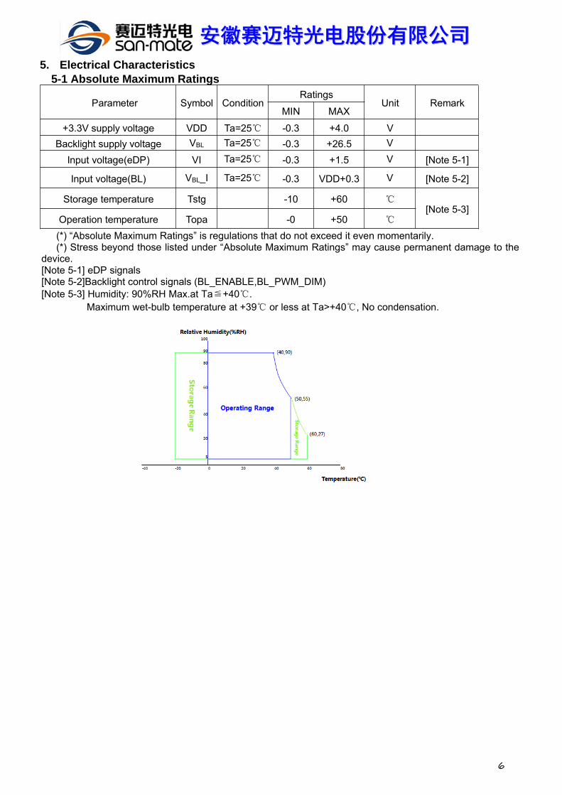
device.[Note 5-1] eDP signals[Note 5-2]Backlight control signals (BL_ENABLE,BL_PWM_DIM)[Note 5-3] Humidity: 90%RH Max.at Ta≦+40℃.
Maximum wet-bulb temperature at +39℃ or less at Ta>+40℃, No condensation.

7
安徽赛迈特光电股份安徽赛迈特光电股份有限公司有限公司5-2 Electrical Specifications
< Electrical specifications > Ta=25+/-2°C

8
安徽赛迈特光电股份安徽赛迈特光电股份有限公司有限公司5.3. DC Characteristics
5-3-1. TFT-LCD panel drivingThe specification of the eDP Rx interface timing parameter is shown in Table 8.
<eDP Rx Interface Timing Specification>

9
安徽赛迈特光电股份安徽赛迈特光电股份有限公司有限公司5-3-2. POWER SEQUENCE
To prevent a latch-up or DC operation of the LCD module, the power on/off sequence shall be as shown in below

10
安徽赛迈特光电股份安徽赛迈特光电股份有限公司有限公司
6 . Backlight drivingThe backlight system is an edge-lighting type with white-LED.(It is usually required to measure under the following condition: Ta=25℃±2℃)
Parameter Symbol Min. Typ. Max. Unit Remark
Supply voltage VBL 6.0 12.0 21.0 V
Current dissipation IBL - 300 - mAVBL=12V
Duty Ratio=100%EN ControlLevel
Backlight on 1.6 - 5 V
[Note6-3-3]Backlight off 0 - 1 V
PWM ControlLevel
VPWMH 1.3 - 5 V
VPWM L 0 - 0.15 V
Brightness ControlDuty Ratio
Duty 1 - 100 % [Note6-3-1]
Brightness Controlfrequency
fPWM 100 - 20,000 Hz
LED lifetime - - 30,000 - h LED
Notes : 1. Power supply voltage12V for LED DriverCalculator Value for reference I F × V F ×40 / efficiency = P LED2. The LED Life-time define as the estimated time to 50% degradation of initial luminous.3. 1% duty cycle is achievable with a dimming frequency less than 1KHz.LED structure
K1
Backlight LED 9串6并54颗 Circuit
K2
K3
K4A
K5
K6

11
安徽赛迈特光电股份安徽赛迈特光电股份有限公司有限公司
7. Timing characteristics of input signals7-1.Timing Characteristics
The TFT-LCM Module is operated by the DE only.
Item Symbols Min Typ Max Unit
ClockFrequency 1/Tc 136.65 147.84 155 MHz
High Time Tch - 4/7 - TcLow Time Tcl - 3/7 - Tc
Frame Period Tv1095 1120 1130 lines- 60 - Hz- 16.7 - ms
Vertical Display Period Tvd - 1080 - lines
One line Scanning Period Th 2080 2200 2248 clocks
Horizontal Display Period Thd - 1920 - clocks
7-2. Input data signals and display position on the screen
Display position of input data(V·H)

12
安徽赛迈特光电股份安徽赛迈特光电股份有限公司有限公司
7-3 Input sigal,basic display colors and gray scale of each color
Each basic color can be displayed in 256 gray scales from 8 bit data signals.According to the combination of 24 bit data signals, the 16.7M color display can be achieved on the screen.

13
安徽赛迈特光电股份安徽赛迈特光电股份有限公司有限公司
8. EDID Specifications (TBD)
00
Header
00 0 0
EDID Header
01 FF 255 255
02 FF 255 255
03 FF 255 255
04 FF 255 255
05 FF 255 255
06 FF 255 255
07 00 0 0
08ID Manufacturer Name
09 9BOE ID = BOE
09 E5 229
0AID Product Code
55 852133 ID = 2133
0B 08 8
0C
32-bit serial No.
00 0 0
0D 00 0 0
0E 00 0 0
0F 00 0 0
10 Week of manufacture 33 51 51
11 Year of Manufacture 1C 28 2018 Manufactured in 2018
12 EDID Structure Ver. 01 1 1 EDID Ver 1.0
13 EDID revision # 04 4 4 EDID Rev. 0.4
14 Video input definition A5 165 - Video Signal Interface
15 Max H image size 1F 31 31 31cm (Approx)
16 Max V image size 11 17 17 17cm (Approx)
17 Display Gamma 78 120 2.2 Gamma curve = 2.2
18 Feature support 02 2 - Feature Support
19 Red/Green low bits FF 255 - Red / Green Low Bits
1A Blue/White low bits 35 53 - Blue / White Low Bits
1B Red x high bits A7 167 0.655 Red(x)= 10100111(0.655)
1C Red y high bits 56 86 0.339 Red(y)= 01010110(0.339)
1D Green x high bits 50 80 0.315 Green(x) = 01010000 0.315)
1E Green y high bits 9F 159 0.624 Green(y) = 10011111 0.624)
1F Blue x high bits 27 39 0.152 Blue(x) = 00100111(0.152)
20 BLue y high bits 0E 14 0.058 Blue(y) = 00001110(0.058)
21 White x high bits 50 80 0.313 White(x) =01010000(0.313)
22 White y high bits 54 84 0.329 White(y)= 01010100 (0.329)
23 Established timing 1 00 0 -
--
24 Established timing 2 00 0 -
25 Established timing 3 00 0 -
26 Standard timing #1 01 1
27 01 1
28 Standard timing #2 01 1
29 01 1

14
安徽赛迈特光电股份安徽赛迈特光电股份有限公司有限公司
2A Standard timing #3 01 1
2B 01 1
2C Standard timing #4 01 1
2D 01 1
2E Standard timing #5 01 1
2F 01 1
30 Standard timing #6 01 1
31 01 1
32 Standard timing #7 01 1
33 01 1
34 Standard timing #8 01 1
35 01 1
36
Detailed timing/monitor
descriptor #1 C0 192 147.8
37 39 57
38 80 128 1920
39 18 24 280
3A 71 113 -
3B 38 56 1080
3C 28 40 40
3D 40 64 -
3E 30 48 48
3F 20 32 32
40 36 54 3
41 00 0 6
42 35 53 309
43 AE 174 174
44 10 16 -
45 00 0 0
46 00 0 0
47 1A 26 -
48
Detailed timing/monitor
descriptor #2 00 0 0.0
49 00 0
4A 00 0 0
4B 00 0 0
4C 00 0 -
4D 00 0 0
4E 00 0 0
4F 00 0 -
50 00 0 0
51 00 0 0
52 00 0 0
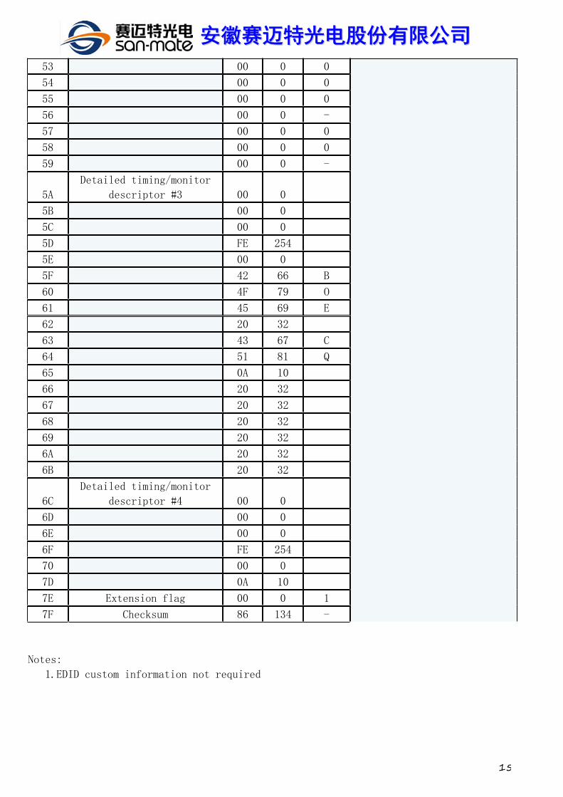
15
安徽赛迈特光电股份安徽赛迈特光电股份有限公司有限公司
53 00 0 0
54 00 0 0
55 00 0 0
56 00 0 -
57 00 0 0
58 00 0 0
59 00 0 -
5A
Detailed timing/monitor
descriptor #3 00 0
5B 00 0
5C 00 0
5D FE 254
5E 00 0
5F 42 66 B
60 4F 79 O
61 45 69 E
62 20 32
63 43 67 C
64 51 81 Q
65 0A 10
66 20 32
67 20 32
68 20 32
69 20 32
6A 20 32
6B 20 32
6C
Detailed timing/monitor
descriptor #4 00 0
6D 00 0
6E 00 0
6F FE 254
70 00 0
7D 0A 10
7E Extension flag 00 0 1
7F Checksum 86 134 -
Notes:
1.EDID custom information not required

16
安徽赛迈特光电股份安徽赛迈特光电股份有限公司有限公司9. OPTICAL SPECIFICATION
9.1 OverviewThe test of Optical specifications shall be measured in a dark room (ambient luminance≤1 lux and
temperature = 25±2℃) with the equipment of Luminance meter system (Goniometer system and PR730) andtest unit shall be located at an approximate distance
50cm from the LCD surface at a viewing angle of θ and Φ equal to 0°, We refer to θØ=0(=θ3 ) as the 3o’clock direction (the “right”), θØ=90 (= θ12 ) as the 12 o’clock direction(“upward”), θØ=180 (= θ9 ) as the 9o’clock direction (“left”) andθØ=270(= θ6 ) as the 6 o’clock direction (“bottom”). While scanning θ and /or Ø, thecenter of the measuring spot on the Display surface shall stay fixed. The backlight should be operating for 30minutes prior to measurement. VDD shall be 3.3+/- 0.3V at 25℃. Optimum viewing angle direction is 6 ’clock.
9.2 ptical characteristics
Paramete Conditions Min. Typ. Max. Unit Note
Viewing Angle(CR>10)
HorizontalθL - 85 -
degreeθR - 85 -
VerticalθT - 85 -
θB - 85 -
Contrast Ratio Center 800 - -
Response Time Tr+Td - 30 35 ms
CF ColorChromaticity(CIE1931)
Red x
Typ.-0.05
0.585
Typ.+0.05
-
[Note 9-2,9-6]Normal operation(PWM Duty=100%)
Red y 0.364 -
Green x 0.350 -
Green y 0.580 -
Blue x 0.163 -
Blue y 0.143 -
White x (0.313) -
White y (0.329) -
NTSC ratio % (75) -
Center Luminance ofwhite
YLI 250 280 cd/m
Cross Talk CT 2.0 %
Notes :1. Viewing angle is the angle at which the contrast ratio is greater than 10. The viewing angles aredetermined for the horizontal or 3, 9 o’clock direction and the vertical or 6, 12 o’clock direction with respectto the optical axis which is normal to the LCD surface (see FIGURE 1).2. Contrast measurements shall be made at viewing angle of Θ= 0 and at the center of the LCD surface.Luminance shall be measured with all pixels in the view field set first to white, then to the dark (black)state .(see FIGURE 1) Luminance Contrast Ratio (CR) is defined mathematically.
3. Center Luminance of white is defined as luminance values of 5 point average across the LCD surface.Luminance shall be measured with all pixels in the view field set first to white. This measurement shall betaken at the locations shown in FIGURE 2 for a total of the measurements per display.4. The White luminance uniformity on LCD surface is then expressed as : ∆Y =Minimum Luminance of5(or 13) points / Maximum Luminance of 5(or 13) points. (see FIGURE 2 and FIGURE 3).5. The color chromaticity coordinates specified in Table 5 shall be calculated from the spectral datameasured with all pixels first in red, green, blue and white. Measurements shall be made at the center ofthe panel.
17
安徽赛迈特光电股份安徽赛迈特光电股份有限公司有限公司
6. The electro-optical response time measurements shall be made as FIGURE 4 by switching the “data”input signal ON and OFF. The times needed for the luminance to change from 10% to 90% is Tr, and 90%to 10% is Td.7. Cross-Talk of one area of the LCD surface by another shall be measured by comparing the luminance(YA) of a 25mm diameter area, with all display pixels set to a gray level, to the luminance (YB) of thatsame area when any adjacent area is driven dark
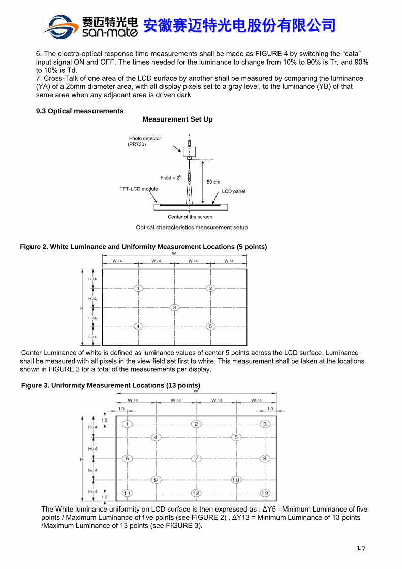
9.3 Optical measurementsMeasurement Set Up
Figure 2. White Luminance and Uniformity Measurement Locations (5 points)
Center Luminance of white is defined as luminance values of center 5 points across the LCD surface. Luminanceshall be measured with all pixels in the view field set first to white. This measurement shall be taken at the locationsshown in FIGURE 2 for a total of the measurements per display.
Figure 3. Uniformity Measurement Locations (13 points)
The White luminance uniformity on LCD surface is then expressed as : ∆Y5 =Minimum Luminance of fivepoints / Maximum Luminance of five points (see FIGURE 2) , ∆Y13 = Minimum Luminance of 13 points/Maximum Luminance of 13 points (see FIGURE 3).

18
安徽赛迈特光电股份安徽赛迈特光电股份有限公司有限公司
Figure 4. Response Time Testing
The electro-optical response time measurements shall be made as shown in FIGURE 4 by switchingthe “data” input signal ON and OFF. The times needed for the luminance to change from 10% to 90% isTd and 90% to 10% is Tr.
Figure 5. Cross Modulation Test Description
Where:Y A = Initial luminance of measured area (cd/m 2 )Y B = Subsequent luminance of measured area (cd/m 2 )
The location measured will be exactly the same in both patterns
Cross-Talk of one area of the LCD surface by another shall be measured bycomparing the luminance (YA) of a 25mm diameter area, with all display pixelsset to a gray level, to the luminance (YB) of that same area when any adjacentarea is driven dark (Refer to FIGURE 5).
10. Display QualityThe display quality of the color TFT-LCD module shall be in compliance with the Incoming Inspection Standard.
11. Handling Precautionsa) Be sure to turn off the power supply when inserting or disconnecting the cable.
Please insert for too much stress not to join a connector in the case of insertion of a connector.b) Be sure to design the cabinet so that the module can be installed without any extra stress such as warp or twist.c) Since the front polarizer is easily damaged, pay attention not to scratch it.d) Wipe off water drop immediately. Long contact with water may cause discoloration or spots.e) When the panel surface is soiled, wipe it with absorbent cotton or other soft cloth.f) Since the panel is made of glass, it may break or crack if dropped or bumped on hard surface. Handle with care.g) Since CMOS LSI is used in this module, take care of static electricity and injure the human earth when handling.
Observe all other precautionary requirements in handling components.h) This module has its circuitry PCBs on the side and should be handled carefully in order not to be stressed.i) Laminate film is attached to the module surface to prevent it from being scratched. Peel the laminate film off
slowly just before the use with strict attention to electrostatic charges. Ionized air shall be blown over during theaction. Blow off the 'dust' on the polarizer by using an ionized nitrogen gun, etc. Working under the followingenvironments is desirable.・All workers wear conductive shoes, conductive clothes, conductive fingerstalls and grounding belts without ail.・Use Ionized blower for electrostatic removal, and peel of the laminate film with a constant speed. (Peeling ofit at over 2 seconds)

19
安徽赛迈特光电股份安徽赛迈特光电股份有限公司有限公司j) The polarizer surface on the panel is treated with Anti-Glare. In case of attaching protective board over the
LCD, be careful about the optical interface fringe etc. which degrades display quality.
k) Do not expose the LCD module to a direct sunlight, for a long period of time to protect the module from theultra violet ray.
l) When handling LCD modules and assembling them into cabinets, please be noted that long-term storage in theenvironment of oxidization or deoxidization gas and the use of such materials as reagent, solvent, adhesive,resin,etc. which generate these gasses, may cause corrosion and discoloration of the LCD modules.
m) Liquid crystal contained in the panel may leak if the LCD is broken. Rinse it as soon as possible if it gets insideyour eye or mouth by mistake.
n) Disassembling the module can cause permanent damage and should be strictly avoided.Please don't remove the fixed tape, insulating tape etc that was pasted on the original module.(Except for protection film of the panel.)
o) Be careful when using it for long time with fixed pattern display as it may cause afterimage.(Please use a screen saver etc., in order to avoid an afterimage.)
p) If a minute particle enters in the module and adheres to an optical material, it may cause display non-uniformityissue, etc. Therefore, fine-pitch filters have to be installed to cooling and inhalation holeif you intend to install a fan.
q) Epoxy resin (amine series curing agent), silicone adhesive material (dealcoholization series and oxime series),tray forming agent (azo compound) etc, in the cabinet or the packing materials may induce abnormal displaywith polarizer film deterioration regardless of contact or noncontact to polarizer film.Be sure to confirm the component of them.
r) Do not use polychloroprene. If you use it, there is some possibility of generating Cl2 gas that influences thereliability of the connection between LCD panel and driver IC.
s) Do not put a laminate film on LCD module, after peeling of the original one. If you put on it, it may causediscoloration or spots because of the occurrence of air gaps between the polarizer and the film.
t) Ground module bezel to stabilize against EMI and external noise.
12. Packaging Condition(TBD)
Piling number of cartonsPackage quantity in one cartonCarton sizeTotal mass of one carton filled with full modulesPacking form
13. Label (TBD)1) Module Bar code label:TBD2) Packing bar code labelTBD
14. RoHS DirectiveThis LCD open-cell is compliant with RoHS Directive.
15. Reliability Test Items
No. Test Item Conditions1 High temperature storage test Ta=60℃ 72h2 Low temperature storage test Ta=-10℃ 72h3 High temperature
& high humidity operation testTa=40℃90%RH 72h(No condensation)
4 High temperature operation test Ta=50℃ 72h5 Low temperature operation test Ta=0℃ 72h[Result Evaluation Criteria] Under the display quality test condition with normal operation state.
Do not change these condition as such changes may affect practical display function.[Normal operation state] temperature:﹢15~﹢35℃,Humidity:45~75%,Atmospheric pressure:86~106kPa

20
安徽赛迈特光电股份安徽赛迈特光电股份有限公司有限公司
设计
检查 核准
确认日
期客
户确
认
修改
内容
下铁
框反
射膜
BEF(增
光片)
导线
印制
电路
板塑
胶框
双面胶
软制
电路
板
上铁
框
发光
二极体
M15
6B30-
54-23
9-020
1
350.76±0.3
344.16(AA)
347.16±
0.3(UP POL)
204.96±0.3
196.59±0.3(UP POL)
193.59(AA)
(175.38)
1.8
3.3
3.03
1.53
(99.83)
11.44
35.75
281.58
BOE
N80 19
20*10
80
2.9±0.2
216.4±1.0
Color coo
rdinat
e:X=0.31
3±0.05,Y
=0.329
±0.05
8.UnSpeci
fied T
olerance
is ±0.2
1.Un
it:mm.
2.Do no
t scale
drawing.
3.All r
adii w
ithout
dimensi
on R0.2.
5.draft a
ngle:
1°
7.Luminac
e unif
ormity:
75%(min)(min
/max*1
00%)
6.Center
lumina
nce :模
组250d/
m^2(Mi
n)~280
d/m^2(
TYP)
4. n Mo
dificati
on Mark.
9.Operati
on con
ditions
:If= 120mA,
Vf=27(
TYP)
Notes:
10.All ma
terial
s comply
with RoHS
11.T
he
measu
red
val
ue of luminace and
colo
r c
oord
ina
te bases FX's BM-7
12:Check
item:1
~9
K1
Backlight LED 9串6并
54颗 Circuit K2K3K4
A
K5K6
130