magnetic nanostructures f. j. himpsel, dept. of physics, uw-madison limits of data storage...
TRANSCRIPT

Magnetic Nanostructures
F. J. Himpsel, Dept. of Physics, UW-Madison
• Limits of Data Storage
• Magnetoelectronics
• One-Dimensional Structures on Silicon
SSSC Meeting, Irvine, Oct. 4, 2001

All of the information ... accumulated in all the books
in the world can be written … in a cube of material
1/200 inch wide.
Use 125 atoms to store one bit.
Richard Feynman
Caltech, December 29th, 1959
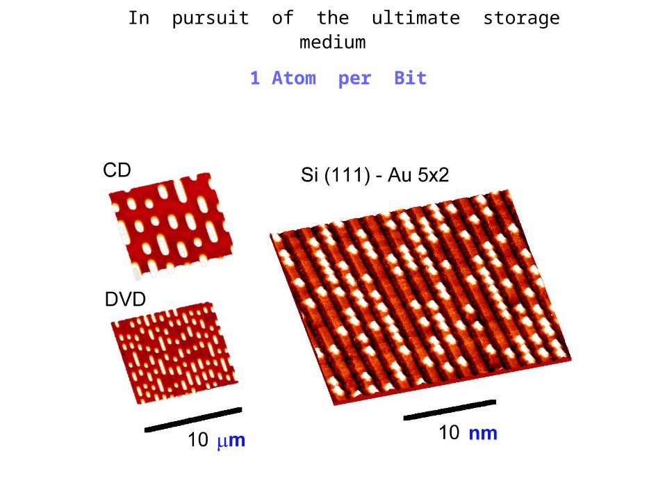
In pursuit of the ultimate storage medium
1 Atom per Bit
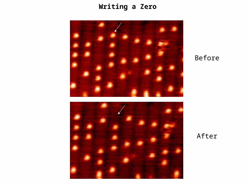
Writing a Zero
Before
After

Filling all Sites
Natural Occupancy:
50%
After Si Evaporation:
100%

Smaller Bits Less Energy Stored Slower Readout
Use Highly-Parallel Readout
Array of Scanning Probes Array of Shift Registers
( Millipede, IBM Zrich ) ( nm m )


50 nm 10 nm particle
Magnetic Storage Media
600nm
17 Gbits/inch2 commercial
Hundreds of particles per bit
Single particle per bit !
Magnetic ForceMicroscopeImage (IBM)

Perfect Magnetic Particles
Sun, Murray , Weller, Folks, Moser,
Science 287, 1989 (2000)
FePt

Giant Magnetoresistance:
Spin-Polarized Tunneling:
Magnetoelectronics
Spin Currents instead of
Charge Currents

Filtering mechanisms
• Interface: Spin-dependent Reflectivity Quantum Well States
• Bulk: Spin-dependent Mean Free Path Magnetic Doping
Parallel Spin Filters Resistance Low
Opposing Spin Filters Resistance High
GMR and Spin - Dependent Scattering
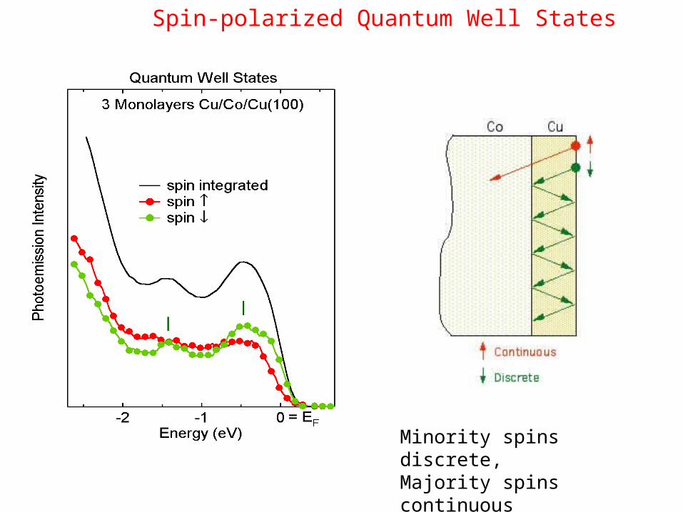
Minority spins discrete,Majority spins continuous
Spin-polarized Quantum Well States

High Resolution Photoemission
States near the Fermi level
determine magneto-transport
( 3.5 kT = 90 meV )
-10
-8
-6
-4
-2
0
2
4
XK
Ni
En
erg
y R
ela
tiv
e t
o E
F [
eV
]
0.7 0.9 1.1
k|| along [011] [Å-1 ]

Magnetic Doping
Magnetic Impurity Selects Spin Carrier
Fe doped

Why Silicon ? Couple Nano- to MicroelectronicsUtilize Silicon Technology
Storage Media: 1 Particle (Atom) per BitAtomically Precise Tracks
Step Arrays as Templates: 2 - 80 nm
1 Kink in 20 000 Atoms
Emulate Lithography: CaF2 Masks Selective Deposition
Atomic Wires: Exotic Electrons in 1D
One-Dimensional Structures on Silicon

Si(111) 77
Control the step spacing
in units of
2.3 nm = 7 atom rows
Step Step
x - Derivative of the STM Topography
“Illumination from the Left Casting Shadows”

Stepped Silicon
Template
1 Kink in
20 000 Atoms
15 nm

Si(557) Regular Step Spacing
5.73 nm

77 Unit + Triple Step
Si(557)
= 17 Atomic Rows

Stepped Silicon Templates
80 nm15 nm6 nm
triple single bunched
Tobacco Mosaic Virus
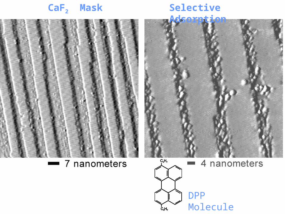
CaF2 Mask Selective Adsorption
DPP Molecule

Selective Deposition
via Photolysis of Ferrocene
Troughs converted to Fe wires

Clean Si(557)
+ Gold
Decoration of Steps Atomic Wires2 nm6 nm

Si(557) - Au

Hole Holon + Spinon
EF
Photoelectron
Spin - Charge Separation
in a One-Dimensional Metal
Zacher, Arrigoni, Hanke, and Schrieffer, PRB 57, 6379 (1998)
Spinon
Holon
EF =
Crossing at EF

Si(557)-Au
• Splitting persists at EF
• Electron count is even
Not spin charge separation
EFermi
Two degenerate orbitals ?
Bonding
Antibonding
E2E1

Tailoring the Electronic Structure
Electron count even,
two bands, metallic
Electron count odd,
one band, “gap”
stepped flat
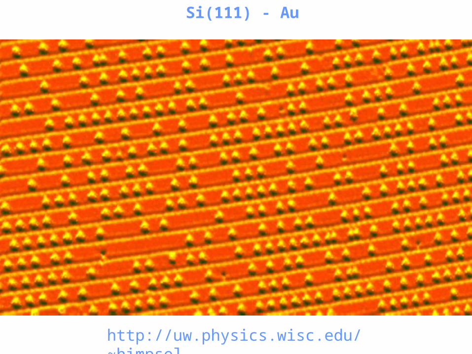
Si(111) - Au
http://uw.physics.wisc.edu/~himpsel