max15046 - maxim
TRANSCRIPT
19-4719; Rev 3; 6/14
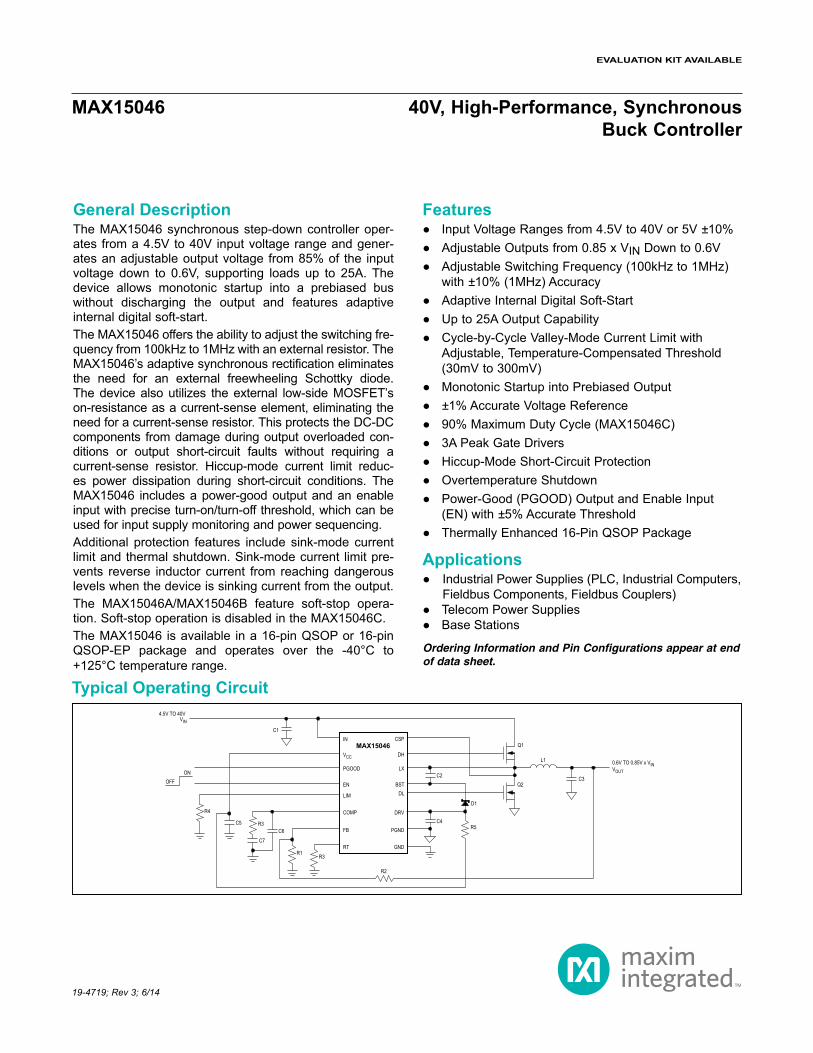
General DescriptionThe MAX15046 synchronous step-down controller oper-ates from a 4.5V to 40V input voltage range and gener-ates an adjustable output voltage from 85% of the input voltage down to 0.6V, supporting loads up to 25A. The device allows monotonic startup into a prebiased bus without discharging the output and features adaptive internal digital soft-start.The MAX15046 offers the ability to adjust the switching fre-quency from 100kHz to 1MHz with an external resistor. The MAX15046’s adaptive synchronous rectification eliminates the need for an external freewheeling Schottky diode. The device also utilizes the external low-side MOSFET’s on-resistance as a current-sense element, eliminating the need for a current-sense resistor. This protects the DC-DC components from damage during output overloaded con-ditions or output short-circuit faults without requiring a current-sense resistor. Hiccup-mode current limit reduc-es power dissipation during short-circuit conditions. The MAX15046 includes a power-good output and an enable input with precise turn-on/turn-off threshold, which can be used for input supply monitoring and power sequencing.Additional protection features include sink-mode current limit and thermal shutdown. Sink-mode current limit pre-vents reverse inductor current from reaching dangerous levels when the device is sinking current from the output.The MAX15046A/MAX15046B feature soft-stop opera-tion. Soft-stop operation is disabled in the MAX15046C.The MAX15046 is available in a 16-pin QSOP or 16-pin QSOP-EP package and operates over the -40°C to +125°C temperature range.
Features Input Voltage Ranges from 4.5V to 40V or 5V ±10% Adjustable Outputs from 0.85 x VIN Down to 0.6V Adjustable Switching Frequency (100kHz to 1MHz)
with ±10% (1MHz) Accuracy Adaptive Internal Digital Soft-Start Up to 25A Output Capability Cycle-by-Cycle Valley-Mode Current Limit with
Adjustable, Temperature-Compensated Threshold (30mV to 300mV)
Monotonic Startup into Prebiased Output ±1% Accurate Voltage Reference 90% Maximum Duty Cycle (MAX15046C) 3A Peak Gate Drivers Hiccup-Mode Short-Circuit Protection Overtemperature Shutdown Power-Good (PGOOD) Output and Enable Input
(EN) with ±5% Accurate Threshold Thermally Enhanced 16-Pin QSOP Package
Applications Industrial Power Supplies (PLC, Industrial Computers,
Fieldbus Components, Fieldbus Couplers) Telecom Power Supplies Base Stations
Ordering Information and Pin Configurations appear at end of data sheet.
MAX15046IN
VCC DH
CSP
LX
BSTDL
DRV
PGND
GND
C1
Q1
Q2
PGOOD
EN
LIM
COMP
FB
RT
L1 0.6V TO 0.85V x VINVOUT
D1
R5C4
C3C2
R2
R3
R3C6
C5
R4
4.5V TO 40V VIN
ONOFF
C7
R1
MAX15046 40V, High-Performance, Synchronous Buck Controller
Typical Operating Circuit
EVALUATION KIT AVAILABLE
IN to GND ..............................................................-0.3V to +45VVCC to GND .................... -0.3V to lower of (VIN + 0.6V) and 6VEN, DRV to GND .....................................................-0.3V to +6VPGOOD to GND ....................................................-0.3V to +45VPGND to GND ......................................................-0.3V to +0.3VDL to PGND ........................................... -0.3V to (VDRV + 0.3V)BST to PGND .......................................................-0.3V to +50VLX and CSP to PGND ..............................................-1V to +45VLX and CSP to PGND ...........................-2V (50ns max) to +45VBST to LX ................................................................-0.3V to +6VCSP to LX .............................................................-0.3V to +0.3VDH to LX ..................................................-0.3V to (VBST + 0.3V)
All Other Pins to GND .............................. -0.3V to (VCC + 0.3V)VCC Short Circuit to GND .........................................ContinuousPGOOD Maximum Sink Current ........................................20mAContinuous Power Dissipation (TA = +70°C): 16-Pin QSOP (derate 9.6mW/°C above +70°C) .......771.5mW 16-Pin QSOP-EP
(derate 22.7mW/°C above +70°C) .........................1818.2mWOperating Temperature Range ......................... -40°C to +125°CJunction Temperature ......................................................+150°CStorage Temperature Range ............................ -65°C to +150°CLead Temperature (soldering, 10s) .................................+300°CSoldering Temperature (reflow) .......................................+260°C
QSOP Junction-to-Ambient Thermal Resistance (θJA) .....+103.7°C/W Junction-to-Case Thermal Resistance (θJC) ...............+37°C/W
QSOP-EP Junction-to-Ambient Thermal Resistance (θJA) ..........+44°C/W Junction-to-Case Thermal Resistance (θJC) .................+6°C/W
(Note 1)
(VIN = 24V, VEN = 5V, VGND = VPGND = 0V, CIN = 1µF, CVCC = 4.7µF, RRT = 49.9kΩ, TA = TJ = -40°C to +125°C, unless otherwisenoted. Typical values are at TA = +25°C.) (Note 2)
PARAMETER SYMBOL CONDITIONS MIN TYP MAX UNITSSYSTEM SPECIFICATIONS
Input-Voltage Range VIN4.5 40
VVIN = VCC = VDRV 4.5 5.5
Quiescent Supply Current IIN_Q VIN = 24V, VFB = 0.9V, no switching 2 3 mA
Shutdown Supply Current IIN_SBYVIN = 24V, VEN = 0V, IVCC = 0, PGOOD = unconnected 0.35 0.55 mA
VCC REGULATOROutput Voltage VCC 6V ≤ VIN ≤ 40V, ILOAD = 6mA 5 5.25 5.5 V
VCC Regulator Dropout VIN = 4.5V, ILOAD = 25mA 0.18 0.45 V
VCC Short-Circuit Output Current VIN = 5V 30 55 90 mA
VCC Undervoltage Lockout VCCUVLO VCC rising 3.8 4 4.2 V
VCC Undervoltage Lockout Hysteresis 400 mV
ERROR AMPLIFIER (FB, COMP)FB Input-Voltage Set Point VFB 584 590 596 mV
FB Input Bias Current IFB VFB = 0.6V -250 +250 nA
FB to COMP Transconductance gM ICOMP = ±20µA 600 1200 1800 µS
Open-Loop Gain 80 dB
Unity-Gain Bandwidth Capacitor from COMP to GND = 47pF 5 MHz
MAX15046 40V, High-Performance, Synchronous Buck Controller
www.maximintegrated.com Maxim Integrated 2
Note 1: Package thermal resistances were obtained using the method described in JEDEC specification JESD51-7, using a four-layer board. For detailed information on package thermal considerations, refer to www.maximintegrated.com/thermal-tutorial.
Absolute Maximum Ratings
Stresses beyond those listed under “Absolute Maximum Ratings” may cause permanent damage to the device. These are stress ratings only, and functional operation of the device at these or any other conditions beyond those indicated in the operational sections of the specifications is not implied. Exposure to absolute maximum rating conditions for extended periods may affect device reliability.
Package Thermal Characteristics
Electrical Characteristics
(VIN = 24V, VEN = 5V, VGND = VPGND = 0V, CIN = 1µF, CVCC = 4.7µF, RRT = 49.9kΩ, TA = TJ = -40°C to +125°C, unless otherwisenoted. Typical values are at TA = +25°C.) (Note 2)
PARAMETER SYMBOL CONDITIONS MIN TYP MAX UNITSVCOMP-RAMP Minimum Voltage 200 mV
COMP Source/Sink Current ICOMP VCOMP = 1.4V 50 80 110 µA
ENABLE (EN)
EN Input High VEN_H VEN rising 1.14 1.20 1.26 V
EN Input Low VEN_L VEN falling 1.05 V
EN Input Leakage Current IEN VEN = 5.5V -1 +1 µA
OSCILLATORSwitching Frequency (100kHz) fSW RRT = 150kΩ 80 100 120 kHz
Switching Frequency (300kHz) fSW RRT = 49.9kΩ 270 300 330 kHz
Switching Frequency (1MHz) fSW RRT = 14.3kΩ 0.9 1 1.1 MHz
Switching Frequency Adjustment Range (Note 3) 100 1000 kHz
RT Voltage VRT RRT = 49.9kΩ 1.15 1.2 1.25 V
PWM MODULATORPWM Ramp Peak-to-Peak Amplitude VRAMP 1.5 V
PWM Ramp Valley VVALLEYMAX15046A/B 1.5
VMAX15046C 0.75
Minimum Controllable On-Time 70 125 ns
Maximum Duty Cycle DMAXfSW = 300kHz (RRT = 49.9kΩ)
MAX15046A/B 85 87.5%
MAX15046C 90 93
Minimum Low-Side On-Time fSW = 1MHz (RRT = 14.3kΩ)
MAX15046A/B 110ns
MAX15046C 90
OUTPUT DRIVERS/DRIVERS SUPPLY (VDRV)Undervoltage Lockout VDRV_UVLO VDRV rising 4.0 4.2 4.4 V
DRV Undervoltage Lockout Hysteresis 400 mV
DH On-ResistanceLow, sinking 100mA, VBST - VLX = 5V 1 3
ΩHigh, sourcing 100mA, VBST - VLX = 5V 1.5 4
DL On-Resistance
Low, sinking 100mA, VDRV = VCC = 5.25V 1 3
High, sourcing 100mA, VDRV = VCC = 5.25V 1.5 4
DH Peak Current CLOAD = 10nF
Sinking, VBST - VLX = 5V 3
ASourcing, VBST - VLX = 5V 2
MAX15046 40V, High-Performance, Synchronous Buck Controller
www.maximintegrated.com Maxim Integrated 3
Electrical Characteristics (continued)
(VIN = 24V, VEN = 5V, VGND = VPGND = 0V, CIN = 1µF, CVCC = 4.7µF, RRT = 49.9kΩ, TA = TJ = -40°C to +125°C, unless otherwisenoted. Typical values are at TA = +25°C.) (Note 2)
Note 2: All devices are 100% tested at room temperature and guaranteed by design over the specified temperature range.
Note 3: Select RRT as:9
RT -7 2SW SW
15.14 10Rf (1 x 10 ) (f )
×=+
, where fSW is in Hertz.
PARAMETER SYMBOL CONDITIONS MIN TYP MAX UNITS
DL Peak Current CLOAD = 10nF
Sinking, VDRV = VCC = 5.25V 3
ASourcing, VDRV = VCC = 5.25V 2
DH, DL Break-Before-Make Time (Dead Time)
MAX15046A/B 10ns
MAX15046C 20
SOFT-START
Soft-Start Duration 2048 Switching Cycles
Reference Voltage Steps 64 Steps
CURRENT LIMIT/HICCUP
Cycle-by-Cycle Valley Current-Limit Threshold Adjustment Range
VCSP - VPGND, valley limit = VLIM/10
VLIM = 0.3V 30mV
VLIM = 3V 300
LIM Reference Current ILIM VLIM = 0.3V to 3V, TA = +25°C 45 50 55 µA
LIM Reference Current Temperature Coefficient 2300 ppm/°C
CSP Input Bias Current VCSP = 40V -1 +1 µA
Number of Consecutive Current-Limit Events to Hiccup 7 Events
Hiccup Timeout 4096 Switching Cycles
Peak Low-Side Sink Current-Limit Threshold
VCSP - VPGND, sink limit = VLIM/20, RILIM = 30kΩ, VLIM = 1.5V, TA = +25°C
75 mV
POWER-GOOD (PGOOD)PGOOD Threshold VFB rising 90 94 97.5 %VFBPGOOD Threshold Hysteresis VFB falling 2.65 %VFBPGOOD Output Low Voltage VPGOOD_L IPGOOD = 2mA, VEN = 0V 0.4 V
PGOOD Output Leakage Current ILEAK_PGOOD VPGOOD = 40V, VEN = 5V, VFB = 1V -1 +1 µA
THERMAL SHUTDOWNThermal Shutdown Threshold Temperature rising +150 °C
Thermal Shutdown Hysteresis 20 °C
MAX15046 40V, High-Performance, Synchronous Buck Controller
www.maximintegrated.com Maxim Integrated 4
Electrical Characteristics (continued)
(VIN = 24V, TA = +25°C, unless otherwise noted.)
EFFICIENCY vs. LOAD CURRENT(VIN = 12V)
MAX
1504
6 to
c02
LOAD CURRENT (A)
EFFI
CIEN
CY (%
)
12963
10
20
30
40
50
60
70
80
90
100
00 15
VOUT = 5VVOUT = 3.3VVOUT = 1.8V
VOUT = 1.2V
VOUT vs. LOAD CURRENT
LOAD CURRENT (A)
% O
UTPU
T FR
OM N
ORMA
L
108642
0.05
0.10
0.15
0.20
0.25
0.30
0.35
0.40
0.45
0.50
00 12
MAX
1504
6 to
c03
VCC vs. LOAD CURRENT
LOAD CURRENT (mA)
V CC
(V)
5.244
5.246
5.248
5.250
5.252
5.254
5.256
5.242
MAX
1504
6 to
c04
4035302520151050 45
VCC LINE REGULATION
VIN (V)
V CC
(V)
35302520151054.0
4.2
4.4
4.6
4.8
5.0
5.2
0 40
MAX
1504
6 to
c05
IVCC = 5mA, 10mA, 20mA, 30mA
IVCC = 40mA
VCC vs. TEMPERATURE
TEMPERATURE (°C)
V CC
(V)
1109580655035205-10-25
5.261
5.262
5.263
5.264
5.265
5.266
5.260-40 125
MAX
1504
6 to
c06
ILOAD = 5mA
SWITCHING FREQUENCYvs. RRT
RRT (kΩ)
FREQ
UENC
Y (kH
z)
1208040
100
200
300
400
500
600
700
800
900
1000
00 160
MAX
1504
6 to
c07
EFFICIENCY vs. LOAD CURRENT(VIN = 24V)
MAX
1504
6 to
c01
LOAD CURRENT (A)
EFFI
CIEN
CY (%
)
12963
10
20
30
40
50
60
70
80
90
100
00 15
VOUT = 5V
VOUT = 3.3V VOUT = 1.8VVOUT = 1.2V
SWITCHING FREQUENCYvs. TEMPERATURE
TEMPERATURE (°C)
FREQ
UENC
Y (kH
z)
1109580655035205-10-25
200
400
600
800
1000
1200
0-40 125
MAX
1504
6 to
c08
RT = 14.3kΩRT = 25.5kΩ
RT = 49.9kΩ
RT = 150kΩ
IIN vs.SWITCHING FREQUENCY
MAX
1504
6 to
c09
FREQUENCY (kHz)
I IN (m
A)
2.3
2.4
2.5
2.6
2.7
2.8
2.2100 1000
CDH = CDL = 0
MAX15046 40V, High-Performance, Synchronous Buck Controller
Maxim Integrated 5www.maximintegrated.com
Typical Operating Characteristics
(VIN = 24V, TA = +25°C, unless otherwise noted.)
SINK AND SOURCE CURRENT LIMITTHRESHOLDS vs. RESISTANCE (RILIM)
RESISTANCE (kΩ)
CURR
ENT-
LIMIT
THR
ESHO
LD (V
)
605030 402010
-0.30-0.25-0.20-0.15-0.10-0.05
00.050.100.150.20
-0.350 70
MAX
1504
6 to
c11
SINK CURRENT LIMIT
SOURCE CURRENT LIMIT
LOAD TRANSIENT ON OUT (1A TO 10A)MAX15046 toc12a
IOUT5A/div
VOUT200mV/div
200µs/div
LOAD TRANSIENT ON OUT (1A TO 15A)MAX15046 toc12b
IOUT5A/div
VOUT200mV/div
200µs/div
LOAD TRANSIENT ON OUT (1A TO 6A)MAX15046 toc12c
IOUT5A/div
VOUT100mV/div
200µs/div
STARTUP DISABLE FROM EN(RLOAD = 3.3Ω) (MAX15046A/B)
MAX15046 toc13
VOUT2V/div
PGOOD5V/div
IN20V/div
EN5V/div
4ms/div
STARTUP AND DISABLE FROM IN(RLOAD = 3.3kΩ)
MAX15046 toc14
VOUT2V/div
PGOOD5V/div
IN10V/div
20ms/div
LIM REFERENCE CURRENT vs. TEMPERATURE
TEMPERATURE (°C)
CURR
ENT
(FA)
11095-25 -10 5 35 50 6520 80
45
50
55
60
65
70
75
80
40-40 125
MAX
1504
6 to
c10
STARTUP WITH PREBIASEDOUTPUT (4.0V)
MAX15046 toc15a
VOUT2V/div
PGOOD5V/div
IN10V/div
24V
4V
4ms/div
STARTUP WITH PREBIASEDOUTPUT (1.0V)
MAX15046 toc15b
VOUT2V/div
PGOOD5V/div
IN10V/div
24V
1V
4ms/div
MAX15046 40V, High-Performance, Synchronous Buck Controller
Maxim Integrated 6www.maximintegrated.com
Typical Operating Characteristics (continued)

(VIN = 24V, TA = +25°C, unless otherwise noted.)
STARTUP WITH PREBIASEDOUTPUT (0.5V)
MAX15046 toc15d
VOUT2V/div
PGOOD5V/div
VIN10V/div
24V
0.5V
4ms/div
VOUT = 3.3V
SINK CURRENT-LIMIT WAVEFORMS(5V PREBIASED)
MAX15046 toc16
VLX50V/div
ILX5A/div
VOUT500mV/div
200µs/div
BREAK-BEFORE-MAKE TIME(DH_ FALLING TO DL_ RISING)
MAX15046 toc17a
VDL5V/div
VLX20V/div
VDH20V/div
40ns/div
BREAK-BEFORE-MAKE TIME(DL_ FALLING TO DH_ RISING)
MAX15046 toc17b
VDL5V/div
VLX20V/div
VDH20V/div
40ns/div
OUTPUT SHORT-CIRCUIT BEHAVIOR MAX15046 toc18
VOUT200mV/div
IOUT10A/div
10ms/div
LINE-TRANSIENT RESPONSEMAX15046 toc19
VIN10V/div
5V
24V
VOUT(AC-COUPLED)200mV/div
10ms/div
STARTUP WITH PREBIASEDOUTPUT (2V)
MAX15046 toc15c
VOUT2V/div
PGOOD5V/div
IN10V/div
24V
2V
4ms/div
VOUT = 3.3V
MAX15046 40V, High-Performance, Synchronous Buck Controller
Maxim Integrated 7www.maximintegrated.com
Typical Operating Characteristics (continued)
PIN NAME FUNCTION
1 IN Regulator Input. Connect to the input rail of the buck converter. Bypass IN to PGND with a 100nF minimum ceramic capacitor. When operating in the 5V ±10% range, connect IN to VCC.
2 VCC
5.25V Linear Regulator Output. Bypass VCC to PGND with a ceramic capacitor of at least 4.7µF when VCC supplies MOSFET gate-driver current at DRV or 2.2µF when VCC is not used to power DRV.
3 PGOOD Open-Drain Power-Good Output. Pull up PGOOD to an external power supply or output with an external resistor.
4 EN Active-High Enable Input. Pull EN to GND to disable the buck converter output. Connect to VCC for always-on operation. EN can be used for power sequencing and as a UVLO adjustment input.
5 LIM Current-Limit Input. Connect a resistor from LIM to GND to program the current-limit threshold from 30mV (RLIM = 6kΩ) to 300mV (RLIM = 60kΩ).
6 COMP Error-Amplifier Output. Connect compensation network from COMP to FB or from COMP to GND.
7 FB Feedback Input (Inverting Input of Error Amplifier). Connect FB to a resistive divider between the buck converter output and GND to adjust the output voltage from 0.6V up to 0.85 x IN.
8 RT Oscillator-Timing Resistor Input. Connect a resistor from RT to GND to set the oscillator frequency from 100kHz to 1MHz.
9 GND Analog Ground. Connect PGND and AGND together at a single point.
10 PGND Power Ground. Use PGND as a return path for the low-side MOSFET gate driver.
11 DRV Gate-Driver Supply Voltage. DRV is internally connected to the low-side driver supply. Bypass DRV to PGND with a 2.2µF minimum ceramic capacitor (see the Typical Application Circuits).
12 DL Low-Side External MOSFET Gate-Driver Output. DL swings from DRV to PGND.
13 BSTBoost Flying Capacitor Connection. Internally connected to the high-side driver supply. Connect a ceramic capacitor of at least 100nF between BST and LX and a diode between BST and DRV for the high-side MOSFET gate-driver supply.
14 LX Inductor Connection. Also serves as a return terminal for the high-side MOSFET driver current. Connect LX to the switching side of the inductor.
15 DH High-Side External MOSFET Gate-Driver Output. DH swings from BST to LX.
16 CSP Current-Sense Positive Input. Connect to the drain of low-side MOSFET with Kelvin connection.
— EP Exposed Pad. Connect EP to a large copper ground plane to maximize thermal performance.
MAX15046 40V, High-Performance, Synchronous Buck Controller
www.maximintegrated.com Maxim Integrated 8
Pin Description

DC-DC OSCILLATOR
ANDENABLELOGIC
EN_INT
VREF
VREF
V_BGAP
BGAP_OK
ENABLECOMPARATOR
BGAP_OK
SHUTDOWN
VL_OK
PWMCOMPARATOR
PWM
DH
BST
LX
CSP
RAMP
HICCUP
VREF
CK
CK
ENABLE
OSCILLATOR
OSC ENABLE
RAMP GENERATOR
BANDGAPOK
GENERATOR
VCC
RT
EN
LIM
VCCUVLO
VIN_OK
IBIAS
VIN_OK
VREF = 0.6V
VBGAP = 1.24V
IN INUVLO
VIN_OKV_BGAP
VDRV_OKDRVUVLO
BGAP_OK
BGAP_OK
V_DRV
INTERNALVOLTAGE
REGULATOR
VIN_OK THERMALSHUTDOWN
AND ILIMCURRENT
GENERATOR
MAINBIAS
CURRENTGENERATOR
BANDGAPREFERENCE
FB
DAC_VREF
HICCUP TIMEOUT
DH_DL_ENABLE
VREF
CK
SOFT-START/STOPAND
HICCUPLOGIC
GM COMP
CK
DH_DL_ENABLE
HICCUP TIMEOUT
PWMCONTROL
LOGIC
LIM/10
LIM/20
SINKCURRENT-LIMITCOMPARATOR
PGOODCOMPARATOR
VALLEYCURRENT-LIMITCOMPARATOR
HIGH-SIDE
DRIVER
HICCUP
MAX15046
DL
DRV
PGND
FB
PGOOD
GND
LOW-SIDE
DRIVER
VREF
ENABLE
MAX15046 40V, High-Performance, Synchronous Buck Controller
www.maximintegrated.com Maxim Integrated 9
Functional Diagram
Detailed DescriptionThe MAX15046 synchronous step-down controller oper-ates from a 4.5V to 40V input-voltage range and gener-ates an adjustable output voltage from 85% of the input-voltage down to 0.6V while supporting loads up to 25A. As long as the device supply voltage is within 5.0V to 5.5V, the input power bus (VIN) can be as low as 3.3V.The MAX15046 offers adjustable switching frequency from 100kHz to 1MHz with an external resistor. The adjustable switching frequency provides design flexibility in selecting passive components. The MAX15046 adopts an adaptive synchronous rectification to eliminate exter-nal freewheeling Schottky diodes and improve efficiency. The device utilizes the on-resistance of the external low-side MOSFET as a current-sense element. The current-limit threshold voltage is resistor-adjustable from 30mV to 300mV and is temperature-compensated, so that the effects of the MOSFET RDS(ON) variation over tempera-ture are reduced. This current-sensing scheme protects the external components from damage during output overloaded conditions or output short-circuit faults without requiring a current-sense resistor. Hiccup-mode current limit reduces power dissipation during short-circuit condi-tions. The MAX15046 includes a power-good output and an enable input with precise turn-on/-off threshold to be used for monitoring and for power sequencing.The MAX15046 features internal digital soft-start that allows prebias startup without discharging the output. The digital soft-start function employs sink current limiting to prevent the regulator from sinking excessive current when the prebias voltage exceeds the programmed steady-state regulation level. The digital soft-start feature prevents the synchronous rectifier MOSFET and the body diode of the high-side MOSFET from experiencing dangerous levels of current while the regulator is sinking current from the output. The MAX15046 shuts down at a +150°C junction temperature to prevent damage to the device.
DC-DC PWM ControllerThe MAX15046 step-down controller uses a PWM volt-age-mode control scheme (see the Functional Diagram). Control-loop compensation is external for providing maxi-mum flexibility in choosing the operating frequency and output LC filter components. An internal transconduc-tance error amplifier produces an integrated error voltage at COMP that helps to provide higher DC accuracy. The voltage at COMP sets the duty cycle using a PWM com-parator and a ramp generator. On the rising edge of an
internal clock, the high-side n-channel MOSFET turns on, and remains on, until either the appropriate duty cycle or the maximum duty cycle is reached. During the on-time of the high-side MOSFET, the inductor current ramps up. During the second-half of the switching cycle, the high-side MOSFET turns off and the low-side n-channel MOSFET turns on. The inductor releases the stored energy as the inductor current ramps down, providing cur-rent to the output. Under overload conditions, when the inductor current exceeds the selected valley current-limit threshold (see the Current-Limit Circuit (LIM) section), the high-side MOSFET does not turn on at the subsequent clock rising edge and the low-side MOSFET remains on to let the inductor current ramp down.
Internal 5.25V Linear RegulatorAn internal linear regulator (VCC) provides a 5.25V nomi-nal supply to power the internal functions and to drive the low-side MOSFET. Connect IN and VCC together when using an external 5V ±10% power supply. The maximum regulator input voltage (VIN) is 40V. Bypass IN to GND with a 1µF ceramic capacitor. Bypass the output of the linear regulator (VCC) with a 4.7µF ceramic capacitor to GND. The VCC dropout voltage is typically 180mV. When VIN is higher than 5.5V, VCC is typically 5.25V. The MAX15046 also employs an undervoltage lockout circuit that disables the internal linear regulator when VCC falls below 3.6V (typical). The 400mV UVLO hysteresis pre-vents chattering on power-up/power-down.
MOSFET Gate Drivers (DH, DL)DH and DL are optimized for driving large-size n-channel power MOSFETs. Under normal operating conditions and after startup, the DL low-side drive waveform is always the complement of the DH high-side drive waveform, with controlled dead time to prevent crossconduction or “shoot-through.” An adaptive dead-time circuit monitors the DH and DL outputs and prevents the opposite-side MOSFET from turning on until the MOSFET is fully off. Thus, the circuit allows the high-side driver to turn on only when the DL gate driver has turned off and prevents the low side (DL) from turning on until the DH gate driver has turned off.The adaptive driver dead time allows operation without shoot-through with a wide range of MOSFETs, minimiz-ing delays and maintaining efficiency. There must be a low-resistance, low-inductance path from DL and DH to the MOSFET gates for the adaptive dead-time circuits to function properly. The stray impedance in the gate
MAX15046 40V, High-Performance, Synchronous Buck Controller
www.maximintegrated.com Maxim Integrated 10
discharge path can cause the sense circuitry to interpret the MOSFET gate as “off” while the VGS of the MOSFET is still high. To minimize stray impedance, use very short, wide traces.Synchronous rectification reduces conduction losses in the rectifier by replacing the normal low-side Schottky catch diode with a low-resistance MOSFET switch. The MAX15046 features a robust internal pulldown transistor with a typical 1Ω RDS(ON) to drive DL low. This low on-resistance prevents DL from being pulled up during the fast rise time of the LX node, due to capacitive coupling from the drain to the gate of the low-side synchronous rectifier MOSFET.
High-Side Gate-Drive Supply (BST)An external Schottky diode between BST and DH is required to boost the gate voltage above LX providing the necessary gate-to-source voltage to turn on the high-side MOSFET. The boost capacitor connected between BST and LX holds up the voltage across the gate driver during the high-side MOSFET on-time.
The charge lost in the boost capacitor for delivering the gate charge is replenished when the high-side MOSFET turns off and the LX node goes to ground. When LX is low, the external diode between VDRV and BST recharges the boost capacitor. See the Boost Capacitor and Diode Selection sections in Applications Information to choose the right boost capacitor and diode.
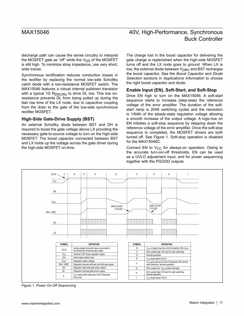
Enable Input (EN), Soft-Start, and Soft-StopDrive EN high to turn on the MAX15046. A soft-start sequence starts to increase (step-wise) the reference voltage of the error amplifier. The duration of the soft-start ramp is 2048 switching cycles and the resolution is 1/64th of the steady-state regulation voltage allowing a smooth increase of the output voltage. A logic-low on EN initiates a soft-stop sequence by stepping down the reference voltage of the error amplifier. Once the soft-stop sequence is completed, the MOSFET drivers are both turned off. See Figure 1. Soft-stop operation is disabled for the MAX15046C.Connect EN to VCC for always-on operation. Owing to the accurate turn-on/-off thresholds, EN can be used as a UVLO adjustment input, and for power sequencing together with the PGOOD outputs.
Figure 1. Power On-Off Sequencing
VCC
B C D E
2048 CLOCKCYCLES
2048 CLOCKCYCLES
F G H IAUVLO
EN
VOUT
DAC_VREF
DH
DL
UVLO Undervoltage threshold value is provided inthe Electrical Characteristics table.Internal 5.25V linear regulator output.Active-high enable input. Regulator output voltage.Regulator internal soft-start and soft-stop signal.Regulator high-side gate-driver output.Regulator low-side gate-driver output.VCC rising while below the UVLO threshold.EN is low.
VCCEN
VOUTDAC_VREF
DHDL
A
SYMBOL DEFINITIONB VCC is higher than the UVLO threshold. EN is low.
EN is pulled high. DH and DL start switching.Normal operation.VCC drops below UVLO.VCC goes above the UVLO threshold. DH and DLstart switching. Normal operation.EN is pulled low. VOUT enters soft-stop.EN is pulled high. DH and DL start switching. Normal operation.VCC drops below UVLO.
CDE
F
G
H
I
SYMBOL DEFINITION
MAX15046 40V, High-Performance, Synchronous Buck Controller
www.maximintegrated.com Maxim Integrated 11
When the valley current limit is reached during soft-start, the MAX15046 regulates to the output impedance times the limited inductor current and turns off after 4096 clock cycles. When starting up into a large capacitive load (for example), the inrush current will not exceed the current-limit value. If the soft-start is not completed before 4096 clock cycles, the device turns off. The device remains off for 8192 clock cycles before trying to soft-start again. This implementation allows the soft-start time to be automati-cally adapted to the time necessary to keep the inductor current below the limit while charging the output capacitor.
Power-Good Output (PGOOD)The MAX15046 includes a power-good comparator to monitor the output voltage and detect the power-good threshold, fixed at 93% of the nominal FB voltage. The open-drain PGOOD output requires an external pullup resistor. PGOOD sinks up to 2mA of current while low.PGOOD goes high (high-Z) when the regulator output increases above 93% of the designed nominal regulated voltage. PGOOD goes low when the regulator output volt-age drops to below 90% of the nominal regulated voltage. PGOOD asserts low during the hiccup timeout period.
Startup into a Prebiased OutputWhen the MAX15046 starts into a prebiased output, DH and DL are off so that the converter does not sink current from the output. DH and DL do not start switching until the PWM comparator commands the first PWM pulse. The first PWM pulse occurs when the ramping reference voltage increases above the FB voltage.When the output voltage is biased above the output set point, the controller tries to pull the output down to the set point once the internal soft-start is complete. This pulldown is controlled by the sink current limit, which is slowly increased to its normal value to minimize output undershoot.
Current-Limit Circuit (LIM)The current-limit circuit employs a ‘valley’ and sink current-sensing algorithm that uses the on-resistance of the low-side MOSFET as a current-sensing element to eliminate costly sense resistors. The current-limit circuit is also temperature-compensated to track the on-resistance variation of the MOSFET overtemperature. The current limit is adjustable with an external resistor at LIM and accommodates MOSFETs with a wide range of on-resistance characteristics (see the Setting the Valley Current Limit section). The adjustment range is from 0.3V to 3V for the valley current limit, corresponding to resistor
values of 6kΩ to 60kΩ. The valley current-limit threshold across the low-side MOSFET is precisely 1/10th of the voltage at LIM, while the sink current-limit threshold is 1/20th of the voltage at LIM.Valley current limit acts when the inductor current flows towards the load, and CSP is more negative than PGND during the low-side MOSFET on-time. If the magnitude of the current-sense signal exceeds the valley current-limit threshold at the end of the low-side MOSFET on-time, the MAX15046 does not initiate a new PWM cycle and lets the inductor current decay in the next cycle. The control-ler also ‘rolls back’ the internal reference voltage so that the controller finds a regulation point determined by the current-limit value and the resistance of the short. In this manner, the controller acts as a constant current source. This method greatly reduces inductor ripple current during the short event, which reduces inductor sizing restrictions and reduces the possibility for audible noise. After 4096 clock cycles, the device goes into hiccup mode. Once the short is removed, the internal reference voltage soft-starts back up to the normal reference voltage and regulation continues.Sink current limit is implemented by monitoring the volt-age drop across the low-side MOSFET when CSP is more positive than PGND. When the voltage drop across the low-side MOSFET exceeds 1/20th of the voltage at LIM at any time during the low-side MOSFET on-time, the low-side MOSFET turns off and the inductor current flows from the output through the body diode of the high-side MOSFET. When the sink current limit activates, the DH/DL switching sequence is no longer complementary and both MOSFETs are turned off.Carefully observe the PCB layout guidelines to ensure that noise and DC errors do not corrupt the current-sense signals at CSP and PGND. Mount the MAX15046 close to the low-side MOSFET with short, direct traces making a Kelvin-sense connection so that trace resistance does not add to RDS(ON) of the low-side MOSFET.
Hiccup Mode Overcurrent ProtectionHiccup mode overcurrent protection reduces power dis-sipation during prolonged short-circuit or severe overload conditions. An internal 3-bit counter counts up on each switching cycle when the valley current-limit threshold is reached. The counter counts down on each switching cycle when the threshold is not reached, and stops at zero (000). When the current-limit condition persists and the counter reaches 111 (= 7 events), the MAX15046 stops both DL and DH drivers and waits for 4096 switching
MAX15046 40V, High-Performance, Synchronous Buck Controller
www.maximintegrated.com Maxim Integrated 12
cycles (hiccup timeout delay) before attempting a new soft-start sequence. The hiccup-mode protection remains active during the soft-start time.
Undervoltage LockoutThe MAX15046 provides an internal undervoltage lockout (UVLO) circuit to monitor the voltage on VCC. The UVLO circuit prevents the MAX15046 from operating when VCC is lower than VUVLO. The UVLO threshold is 4V, with 400mV hysteresis to prevent chattering on the rising/falling edge of the supply voltage. DL and DH stay low to inhibit switching when the device is in undervoltage lockout.
Thermal-Overload ProtectionThermal-overload protection limits total power dissipation in the MAX15046. When the junction temperature of the device exceeds +150°C, an on-chip thermal sensor shuts down the device, forcing DL and DH low, which allows the device to cool. The thermal sensor turns the device on again after the junction temperature cools by 20°C. The regulator shuts down and soft-start resets during thermal shutdown. Power dissipation in the LDO regulator and excessive driving losses at DH/DL trigger thermal-overload protection. Carefully evaluate the total power dissipation (see the Power Dissipation section) to avoid unwanted triggering of the thermal-overload protection in normal operation.
Applications InformationEffective Input-Voltage RangeThe MAX15046 operates from 4.5V to 40V input supplies and regulates output down to 0.6V. The minimum voltage conversion ratio (VOUT/VIN) is limited by the minimum controllable on-time. For proper fixed-frequency PWM operation, the voltage conversion ratio must obey the fol-lowing condition:
OUTON(MIN) SW
IN
V t fV
> ×
where tON(MIN) is 125ns and fSW is the switching fre-quency in Hertz. Pulse skipping occurs to decrease the effective duty cycle when the desired voltage conversion does not meet the above condition. Decrease the switch-ing frequency or lower the input voltage VIN to avoid pulse skipping.
The maximum voltage conversion ratio is limited by the maximum duty cycle (Dmax):
OUT max DROP2 max DROP1max
IN IN
V D V (1-D ) VD -V V
× + ×<
where VDROP1 is the sum of the parasitic voltage drops in the inductor discharge path, including synchronous recti-fier, inductor, and PCB resistance. VDROP2 is the sum of the voltage drops by the resistance in the charging path, including high-side switch, inductor, and PCB resistance. In practice, provide adequate margin to the above condi-tions for good load-transient response.
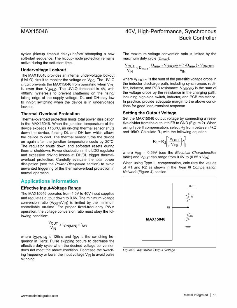
Setting the Output VoltageSet the MAX15046 output voltage by connecting a resis-tive divider from the output to FB to GND (Figure 2). When using Type II compensation, select R2 from between 4kΩ and 16kΩ. Calculate R1 with the following equation:
OUT1 2
FB
VR R -1V
=
where VFB = 0.59V (see the Electrical Characteristics table) and VOUT can range from 0.6V to (0.85 x VIN).When using Type III compensation, calculate the values of R1 and R2 as shown in the Type III Compensation Network (Figure 4) section.
Figure 2. Adjustable Output Voltage
FB
R1
OUT
R2MAX15046
MAX15046 40V, High-Performance, Synchronous Buck Controller
www.maximintegrated.com Maxim Integrated 13
Setting the Switching FrequencyAn external resistor connecting RT to GND sets the switching frequency (fSW). The relationship between fSW and RRT is:
9RT -7 2
SW SW
15.14 10Rf (1 x 10 ) (f )
×=+
where fSW is in Hz and RRT is in Ω. For example, a 300kHz switching frequency is set with RRT = 49.9kΩ. Higher frequencies allow designs with lower inductor values and less output capacitance. Peak currents and I2R losses are lower at higher switching frequencies, but core losses, gate-charge currents, and switching losses increase.
Inductor SelectionThree key inductor parameters must be specified for oper-ation with the MAX15046: inductance value (L), inductor saturation current (ISAT), and DC resistance (RDC). To determine the inductance, select the ratio of inductor peak-to-peak AC current to DC average current (LIR) first. For LIR values that are too high, the RMS currents are high, and, therefore, I2R losses are high. Use high-valued inductors to achieve low LIR values. Typically, inductor resistance is proportional to inductance for a given pack-age type, which again makes I2R losses high for very low LIR values. A good compromise between size and loss is a 30% peak-to-peak ripple current to average-current ratio (LIR = 0.3). The switching frequency, input voltage, output voltage, and selected LIR determine the inductor value as follows:
OUT IN OUTIN SW OUT
V (V - V )LV f I LIR
=× × ×
where VIN, VOUT, and IOUT are typical values. The switching frequency is set by RT (see Setting the Switching Frequency section). The exact inductor value is not critical and can be adjusted to make trade-offs among size, cost, and efficiency. Lower inductor values minimize size and cost, but also improve transient response and reduce efficiency due to higher peak currents. On the other hand, higher inductance increases efficiency by reducing the RMS current.Find a low-loss inductor with the lowest possible DC resis-tance that fits in the allotted dimensions. The saturation current rating (ISAT) must be high enough to ensure that saturation cannot occur below the maximum current-limit value (ICL(MAX)), given the tolerance of the on-resistance of the low-side MOSFET and of the LIM reference current
(ILIM). Combining these conditions, select an inductor with a saturation current (ISAT) of:
ISAT ≥ 1.35 ×ICL(TYP)where ICL(TYP) is the typical current-limit set point. The factor 1.35 includes RDS(ON) variation of 25% and 10% for the LIM reference current error. A variety of inductors from different manufacturers are available to meet this requirement (for example, Vishay IHLP-4040DZ-1-5 and other inductors from the same series).
Setting the Valley Current LimitThe minimum current-limit threshold must be high enough to support the maximum expected load current with the worst-case low-side MOSFET on-resistance value as the RDS(ON) of the low-side MOSFET is used as the current-sense element. The inductor’s valley current occurs at ILOAD(MAX) minus one half of the ripple current. The mini-mum value of the current-limit threshold voltage (VITH) must be higher than the voltage on the low-side MOSFET during the ripple-current valley,
ITH DS(ON,MAX) LOAD(MAX)LIRV R I 12
− > × ×
where RDS(ON,MAX) in Ω is the maximum on-resistance of the low-side MOSFET at maximum load current ILOAD(MAX) and is calculated from the following equation:
DS(ON,MAX) DS(ON)
MOSFET MAX AMB
R R
[1 TC (T - T )]
= ×
+ ×
where RDS(ON) (in Ω is the on-resistance of the low-side MOSFET at ambient temperature TAMB (in degrees Celsius), TCMOSFET is the temperature coefficient of the low-side MOSFET in ppm/°C, and TMAX (in degrees Celsius) is the temperature at maximum load current ILOAD(MAX). Obtain the RDS(ON) and TCMOSFET from the MOSFET data sheet.Connect an external resistor (RLIM) from LIM to GND to adjust the current-limit threshold, which is temper-ature-compensated with a temperature coefficient of 2300ppm/°C. The relationship between the current-limit threshold (VITH) and RLIM is:
ITHLIM
-6MAX AMB)
10 VRppm50 10 1 2300 (T - T
C
×=
× × + × °
where RLIM is in Ω, VITH is in V, TMAX and TAMB are in °C.
MAX15046 40V, High-Performance, Synchronous Buck Controller
www.maximintegrated.com Maxim Integrated 14
An RLIM resistance range of 6kΩ to 60kΩ corresponds to a current-limit threshold of 30mV to 300mV. Use 1% toler-ance resistors when adjusting the current limit to minimize error in the current-limit threshold.
Input CapacitorThe input filter capacitor reduces peak current drawn from the power source and reduces noise and voltage ripple on the input caused by the switching circuitry. The input capacitor must meet the ripple current requirement (IRMS) imposed by the switching currents as defined by the fol-lowing equation:
OUT IN OUTRMS LOAD(MAX)
IN
V (V - V )I I
V=
IRMS attains a maximum value when the input volt-age equals twice the output voltage (VIN = 2VOUT), so IRMS(MAX) = ILOAD(MAX)/2. For most applications, nontantalum capacitors (ceramic, aluminum, polymer, or OS-CON) are preferred at the inputs due to the robust-ness of nontantalum capacitors to accommodate high inrush currents of systems being powered from very low impedance sources. Additionally, two (or more) smaller-value low-ESR capacitors should be connected in parallel to reduce high-frequency noise.
Output CapacitorThe key selection parameters for the output capacitor are capacitance value, ESR, and voltage rating. These parameters affect the overall stability, output ripple volt-age, and transient response. The output ripple has two components: variations in the charge stored in the output capacitor, and the voltage drop across the capacitor’s ESR caused by the current flowing into and out of the capacitor:
ΔVRIPPLE = ΔVESR + ΔVQThe output-voltage ripple as a consequence of the ESR and the output capacitance is:
ESR P-P
P-PQ
OUT SW
IN OUT OUTP-P
SW IN
V I ESRIV
8 C f
V - V VIf L V
∆ = ×
∆ =× ×
= × ×
where IP-P is the peak-to-peak inductor current ripple (see the Inductor Selection section). Use these equations for initial capacitor selection. Decide on the final values by testing a prototype or an evaluation circuit.
Check the output capacitor against load-transient response requirements. The allowable deviation of the output voltage during fast load transients determines the capacitor output capacitance, ESR, and equivalent series inductance (ESL). The output capacitor supplies the load current during a load step until the controller responds with a higher duty cycle. The response time (tRESPONSE) depends on the closed-loop bandwidth of the converter (see the Compensation Design section). The resistive drop across the ESR of the output capacitor, the voltage drop across the ESL (ΔVESL) of the capacitor, and the capacitor discharge, cause a voltage droop during the load step.Use a combination of low-ESR tantalum/aluminum elec-trolytic and ceramic capacitors for improved transient load and voltage ripple performance. Nonleaded capacitors and capacitors in parallel help reduce the ESL. Keep the maximum output-voltage deviation below the tolerable limits of the load. Use the following equations to calculate the required ESR, ESL, and capacitance value during a load step:
ESRSTEP
STEP RESPONSEOUT
Q
ESL STEPSTEP
RESPONSEO
VESRI
I tCV
V tESLI
1t3 f
∆=
×=
∆
∆ ×=
≅×
where ISTEP is the load step, tSTEP is the rise time of the load step, tRESPONSE is the response time of the control-ler, and fO is the closed-loop crossover frequency.
Compensation DesignThe MAX15046 provides an internal transconductance amplifier with the inverting input and the output avail-able for external frequency compensation. The flexibility of external compensation offers wide selection of output filtering components, especially the output capacitor. Use high-ESR aluminum electrolytic capacitors for cost-sensitive applications. Use low-ESR tantalum or ceramic capacitors at the output for size-sensitive applications. The high switching frequency of the MAX15046 allows the use of ceramic capacitors at the output. Choose all passive power components to meet the output ripple, component size, and component cost requirements. Choose the com-pensation components for the error amplifier to achieve the desired closed-loop bandwidth and phase margin.
MAX15046 40V, High-Performance, Synchronous Buck Controller
www.maximintegrated.com Maxim Integrated 15
To choose the appropriate compensation network type, the power-supply poles and zeros, the zero-crossover frequency, and the type of the output capacitor must be determined first.In a buck converter, the LC filter in the output stage intro-duces a pair of complex poles at the following frequency:
POOUT OUT
1f2 L C
=π× ×
The output capacitor introduces a zero at:
ZOOUT
1f2 ESR C
=π× ×
where ESR is the equivalent series resistance of the out-put capacitor.The loop-gain crossover frequency (fO), where the loop gain equals 1 (0dB) should be set below 1/10th of the switching frequency:
SWO
ff10
≤
Choosing a lower crossover frequency reduces the effects of noise pickup into the feedback loop, such as jittery duty cycle.To maintain a stable system, two stability criteria must be met:1) The phase shift at the crossover frequency, fO, must
be less than 180°. In other words, the phase margin of the loop must be greater than zero.
2) The gain at the frequency where the phase shift is -180° (gain margin) must be less than 1.
Maintain a phase margin of around 60° to achieve a robust loop stability and well-behaved transient response.When using an electrolytic or large-ESR tantalum output capacitor, the capacitor ESR zero fZO typically occurs between the LC poles and the crossover frequency fO (fPO < fZO < fO). Choose the Type II (PI-Proportional, Integral) compensation network.When using a ceramic or low-ESR tantalum output capacitor, the capacitor ESR zero typically occurs above the desired crossover frequency fO, that is fPO < fO < fZO. Choose the Type III (PID- Proportional, Integral, and Derivative) compensation network.
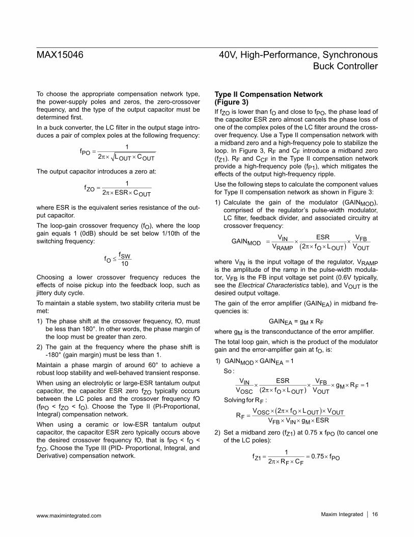
Type II Compensation Network (Figure 3)If fZO is lower than fO and close to fPO, the phase lead of the capacitor ESR zero almost cancels the phase loss of one of the complex poles of the LC filter around the cross-over frequency. Use a Type II compensation network with a midband zero and a high-frequency pole to stabilize the loop. In Figure 3, RF and CF introduce a midband zero (fZ1). RF and CCF in the Type II compensation network provide a high-frequency pole (fP1), which mitigates the effects of the output high-frequency ripple.Use the following steps to calculate the component values for Type II compensation network as shown in Figure 3:1) Calculate the gain of the modulator (GAINMOD),
comprised of the regulator’s pulse-width modulator, LC filter, feedback divider, and associated circuitry at crossover frequency:
( )IN FB
MODRAMP O OUT OUT
V VESRGAINV 2 f L V
= × ×π× ×
where VIN is the input voltage of the regulator, VRAMP is the amplitude of the ramp in the pulse-width modula-tor, VFB is the FB input voltage set point (0.6V typically, see the Electrical Characteristics table), and VOUT is the desired output voltage.The gain of the error amplifier (GAINEA) in midband fre-quencies is:
GAINEA = gM x RFwhere gM is the transconductance of the error amplifier.The total loop gain, which is the product of the modulator gain and the error-amplifier gain at fO, is:
( )
MOD EA
IN FBM F
OSC O OUT OUT
F
OSC O OUT OUTF
FB IN M
1) GAIN GAIN 1So :
V VESR g R 1V (2 f L ) V
Solving for R :V 2 f L V
RV V g ESR
× =
× × × × =π× ×
× π× × ×=
× × ×
2) Set a midband zero (fZ1) at 0.75 x fPO (to cancel one of the LC poles):
Z1 POF F
1f 0.75 f2 R C
= = ×π× ×
MAX15046 40V, High-Performance, Synchronous Buck Controller
www.maximintegrated.com Maxim Integrated 16
Solving for CF:
FF PO
1C2 R f 0.75
=π× × ×
3) Place a high-frequency pole at fP1 = 0.5 x fSW (to attenuate the ripple at the switching frequency fSW) and calculate CCF using the following equation:
CFF SW
F
1C 1R f -C
=π× ×
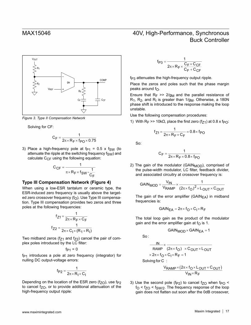
Type III Compensation Network (Figure 4)When using a low-ESR tantalum or ceramic type, the ESR-induced zero frequency is usually above the target-ed zero crossover frequency (fO). Use Type III compensa-tion. Type III compensation provides two zeros and three poles at the following frequencies:
Z1F F
Z2I 1 I
1f2 R C
1f2 C (R R )
=π× ×
=π× × +
Two midband zeros (fZ1 and fZ2) cancel the pair of com-plex poles introduced by the LC filter:
fP1 = 0fP1 introduces a pole at zero frequency (integrator) for nulling DC output-voltage errors:
P2I I
1f2 R C
=π× ×
Depending on the location of the ESR zero (fZO), use fP2 to cancel fZO, or to provide additional attenuation of the high-frequency output ripple:
P3F CF
FF CF
1f C C2 RC C
=×
π× ×+
fP3 attenuates the high-frequency output ripple.Place the zeros and poles such that the phase margin peaks around fO.Ensure that RF >> 2/gM and the parallel resistance of R1, R2, and RI is greater than 1/gM. Otherwise, a 180N phase shift is introduced to the response making the loop unstable.Use the following compensation procedures:1) With RF >> 10kΩ, place the first zero (fZ1) at 0.8 x fPO:
Z1 POF F
1f 0.8 f2 R C
= = ×π× ×
So:
FF PO
1C2 R 0.8 f
=π× × ×
2) The gain of the modulator (GAINMOD), comprised of the pulse-width modulator, LC filter, feedback divider, and associated circuitry at crossover frequency is:
INMOD 2RAMP O OUT OUT
V 1GAINV (2 f ) L C
= ×π× × ×
The gain of the error amplifier (GAINEA) in midband frequencies is:
EA O I FGAIN 2 f C R= π× × ×
The total loop gain as the product of the modulator gain and the error amplifier gain at fO is 1.
( )
MOD EA
INRAMP O OUT OUT
O I F
RAMP O OUT OUT
IN F
GAIN GAIN 1So :
(2 f ) C L2 f C R 1
Solving for C :V 2 f L C
V R
× =
×π× × ×
× π× × × =
× π× × ××
3) Use the second pole (fP2) to cancel fZO when fPO < fO < fZO < fSW/2. The frequency response of the loop gain does not flatten out soon after the 0dB crossover,
Figure 3. Type II Compensation Network
VREF
R1
VOUT
R2gM
RF
COMP
CF CCF
MAX15046 40V, High-Performance, Synchronous Buck Controller
www.maximintegrated.com Maxim Integrated 17
and maintains -20dB/decade slope up to 1/2 of the switching frequency. This is likely to occur if the output capacitor is low-ESR tantalum. Set fP2 = fZO.
When using a ceramic capacitor, the capacitor ESR zero (fZO) is likely to be located even above one half of the switching frequency, fPO < fO < fSW/2 < fZO. In this case, place the frequency of the second pole (fP2) high enough in order not to significantly erode the phase margin at the crossover frequency. For example, set fP2 at 5 x fO so that the contribution to phase loss at the crossover fre-quency fO is only about 11°:
fP2 = 5 x fOOnce fP2 is known, calculate RI:
IP2 I
1R2 f C
=π× ×
4) Place the second zero (fZ2) at 0.2 x fO or at fPO, whichever is lower and calculate R1 using the following equation:
1 IZ2 I
1R - R2 f C
=π× ×
5) Place the third pole (fP3) at one half the switching fre-quency and calculate CCF:
( )F
CFSW F F
CC2 0.5 f R C - 1
=π× × × ×
6) Calculate R2 as:
FB2 1
OUT FB
VR RV V
= ×−
MOSFET SelectionThe MAX15046 step-down controller drives two exter-nal logic-level n-channel MOSFETs. The key selection parameters to choose these MOSFETs include:
On-resistance (RDS(ON)) Maximum Drain-to-Source Voltage (VDS(MAX)) Minimum Threshold Voltage (VTH(MIN)) Total Gate Charge (QG) Reverse Transfer Capacitance (CRSS) Power Dissipation
The two n-channel MOSFETs must be a logic-level type with guaranteed on-resistance specifications at VGS = 4.5V. For maximum efficiency, choose a high-side MOSFET that has conduction losses equal to the switching losses at the typical input voltage. Ensure that the conduction losses at minimum input voltage do not exceed the MOSFET package thermal limits, or violate the overall thermal budget. Also ensure that the conduc-tion losses plus switching losses at the maximum input voltage do not exceed package ratings or violate the overall thermal budget. Ensure that the DL gate driver can drive the low-side MOSFET. In particular, check that the dv/dt caused by the high-side MOSFET turning on does not pull up the low-side MOSFET gate through the drain-to-gate capacitance of the low-side MOSFET, which is the most frequent cause of crossconduction problems.Check power dissipation when using the internal linear regulator to power the gate drivers. Select MOSFETs with low gate charge so that VCC can power both drivers with-out overheating the device:
PDRIVE = VCC x QG_TOTAL x fSWwhere QG_TOTAL is the sum of the gate charges of the two external MOSFETs.
Boost Capacitor and Diode SelectionThe MAX15046 uses a bootstrap circuit to generate the necessary gate-to-source voltage to turn on the high-side MOSFET. The selected n-channel high-side MOSFET determines the appropriate boost capacitance value (CBST in the Typical Application Circuits) according to the following equation:
GBST
BST
QCV
=∆
where QG is the total gate charge of the high-side MOSFET and ΔVBST is the voltage variation allowed on the high-side MOSFET driver after turn-on. Choose Figure 4. Type III Compensation Network
VREF
gM
R1
R2
VOUT
RI
COMP
CI
CCF
RF CF
MAX15046 40V, High-Performance, Synchronous Buck Controller
www.maximintegrated.com Maxim Integrated 18
ΔVBST such that the available gate-drive voltage is not significantly degraded (e.g. ΔVBST = 100mV to 300mV) when determining CBST.Use a low-ESR ceramic capacitor as the boost capacitor with a minimum value of 100nF.A small-signal diode can be used for the bootstrap circuit and must have a minimum voltage rating of VIN + 3V to withstand the maximum BST voltage. The average forward current of the diode should meet the following requirement:
IF > QGATE x fSWwhere QGATE is the gate charges of the high-side MOSFET.
Power DissipationThe maximum power dissipation of the device depends on the thermal resistance from the die to the ambient environment and the ambient temperature. The thermal resistance depends on the device package, PCB copper area, other thermal mass, and airflow.The power dissipated into the package (PT) depends on the supply configuration (see the Typical Application Circuits). Use the following equation to calculate power dissipation:
PT = VIN x [QG_TOTAL x fSW + IQ]where IQ is the quiescent supply current at the switching frequency. See the IIN vs. Switching Frequency graph in the Typical Operating Characteristics for the IQ.Use the following equation to estimate the temperature rise of the die:
TJ = TA + (PT x θJA)where θJA is the junction-to-ambient thermal impedance of the package, PT is power dissipated in the device, and TA is the ambient temperature. The θJA is 103.7°C/W for the 16-pin QSOP and 44°C/W for the 16-pin QSOP-EP package on multilayer boards, with the conditions specified by the respective JEDEC standards (JESD51-5, JESD51-7). An accurate estimation of the junction tem-perature requires a direct measurement of the case temperature (TC) when actual operating conditions sig-nificantly deviate from those described in the JEDEC standards. The junction temperature is then:
TJ = TC + (PT x θJC)Use 37°C/W as θJC thermal impedance for the 16-pin QSOP package and 6°C/W for the 16-pin QSOP-EP
package. The case-to-ambient thermal impedance (θCA) is dependent on how well the heat is transferred from the PCB to the ambient. Use large copper areas to keep the PCB temperature low.
PCB Layout GuidelinesCareful PCB layout is critical to achieve clean and stable operation. The switching power stage requires particular attention. Follow these guidelines for good PCB layout:1) Place decoupling capacitors as close as possible to
the IC. Connect the power ground plane (connected to PGND) and signal ground plane (connected to GND) at one point near the device.
2) Connect input and output capacitors to the power ground plane; connect all other capacitors to the signal ground plane.
3) Keep the high-current paths as short and wide as pos-sible. Keep the path of switching current (C2 to IN and C2 to PGND) short. Avoid vias in the switching paths.
4) Connect CSP to the drain of the low-side FET using a Kelvin connection for accurate current-limit sensing.
5) Ensure all feedback connections are short and direct. Place the feedback resistors as close as possible to the IC.
6) Route high-speed switching nodes (BST, LX, DH, and DL) away from sensitive analog areas (RT, FB, COMP, and LIM).
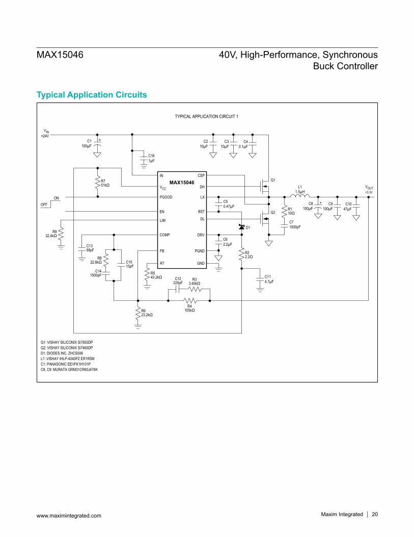
24V Supply, 3.3V Output OperationTypical Application Circuit 1 in the Typical Application Circuits section shows an application circuit that operates out of 24V and outputs up to 10A at 3.3V. R5 sets the switching frequency to 350kHz.
Single 4.5V to 5.5V Supply OperationTypical Application Circuit 2 in the Typical Application Circuits section shows an application circuit for a single +4.5V to +5.5V power-supply operation.
Auxiliary 5V Supply OperationTypical Application Circuit 3 in the Typical Application Circuits section shows an application circuit for a +24V supply to drive the external MOSFETs and an auxiliary +5V supply to power the device
MAX15046 40V, High-Performance, Synchronous Buck Controller
www.maximintegrated.com Maxim Integrated 19
MAX15046IN
TYPICAL APPLICATION CIRCUIT 1
VCC DH
CSP
LX
BST
DL
DRV
PGND
GND
Q1
Q1: VISHAY SILICONIX Si7850DPQ2: VISHAY SILICONIX Si7460DPD1: DIODES INC. ZHCS506L1: VISHAY IHLP-4040PZ ER1R5MC1: PANASONIC EEVFK1H101PC8, C9: MURATA GRM31CR60J476K
Q2
PGOOD
EN
LIM
COMP
FB
RT
L11.5µH
VOUT+3.3V
D1
C62.2µF
C8100µF
C1047µF
C40.1µF
C310µF
C210µF
C50.47µF
R4105kΩ
R543.2kΩ
C161µF
R932.4kΩ
VIN+24V
C1368pF
C1515pF
C12220pF
C141500pF
R623.2kΩ
C1100µF
R22.2Ω
R751kΩ
ONOFF
R822.6kΩ
R33.65kΩ
C114.7µF
C9100µFR1
10Ω
C71000pF
MAX15046 40V, High-Performance, Synchronous Buck Controller
www.maximintegrated.com Maxim Integrated 20
Typical Application Circuits
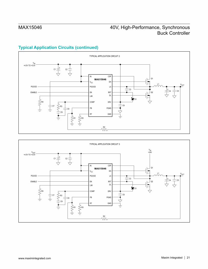
MAX15046IN
VCC DH
CSP
LX
BSTDL
DRV
PGND
GND
C2
Q1
Q2
PGOOD
EN
LIM
COMP
FB
RT
L1 VOUT
D1
C6
C4 C5C3
R2
R3
R3C8
C7
R4
VIN+4.5V TO +5.5V
PGOOD
ENABLE
C9
R1
C1
TYPICAL APPLICATION CIRCUIT 2
MAX15046IN
VCC DH
CSP
LX
BSTDL
DRV
PGND
GND
C2
Q1
Q2
PGOOD
EN
LIM
COMP
FB
RT
L1 VOUT
D1
C6
C4 C5C3
R2
R3
R3C8
C7
R4
VAUX+4.5V TO +5.5V
VIN+24V
PGOOD
ENABLE
C9
R1
C1
TYPICAL APPLICATION CIRCUIT 3
Typical Application Circuits (continued)
MAX15046 40V, High-Performance, Synchronous Buck Controller
www.maximintegrated.com Maxim Integrated 21
+Denotes lead(Pb)-free/RoHS-compliant package.*EP = Exposed pad.The MAX15046C is recommended for new designs.
PART TEMP RANGE PIN-PACKAGE
MAX15046AAEE+ -40°C to +125°C 16 QSOP
MAX15046BAEE+ -40°C to +125°C 16 QSOP-EP*
MAX15046CAEE+ -40°C to +125°C 16 QSOP-EP*PACKAGE TYPE PACKAGE CODE OUTLINE NO.
16 QSOP E16+4 21-0055
16 QSOP-EP E16E+9 21-0055
16
15
14
13
12
11
10
9
1
2
3
4
5
6
7
8
IN CSP
DH
LX
BST
DL
DRV
PGND
GND
TOP VIEW
MAX15046A
QSOP
VCC
PGOOD
COMP
EN
LIM
FB
RT
+ 16
15
14
13
12
11
10
9
1
2
3
4
5
6
7
8
IN CSP
DH
LX
BST
DL
DRV
PGND
GND
QSOP-EP
VCC
PGOOD
COMP
EN
LIM
FB
RT
EXPOSEDPAD
+
MAX15046BMAX15046C
MAX15046 40V, High-Performance, Synchronous Buck Controller
www.maximintegrated.com Maxim Integrated 22
Package InformationFor the latest package outline information and land patterns (footprints), go to www.maximintegrated.com/packages. Note that a “+”, “#”, or “-” in the package code indicates RoHS status only. Package drawings may show a different suffix character, but the drawing pertains to the package regardless of RoHS status.
Chip InformationPROCESS: BiCMOS
Pin Configurations
Ordering Information
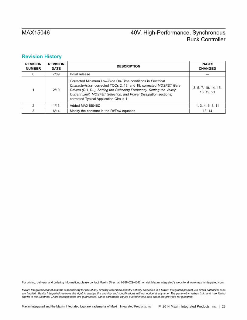
REVISIONNUMBER
REVISION DATE DESCRIPTION PAGES
CHANGED0 7/09 Initial release —
1 2/10
Corrected Minimum Low-Side On-Time conditions in Electrical Characteristics; corrected TOCs 2, 18, and 19; corrected MOSFET Gate Drivers (DH, DL), Setting the Switching Frequency, Setting the Valley Current Limit, MOSFET Selection, and Power Dissipation sections; corrected Typical Application Circuit 1
3, 5, 7, 10, 14, 15, 18, 19, 21
2 1/13 Added MAX15046C 1, 3, 4, 6–8, 113 6/14 Modify the constant in the Rt/Fsw equation 13, 14
Maxim Integrated cannot assume responsibility for use of any circuitry other than circuitry entirely embodied in a Maxim Integrated product. No circuit patent licenses are implied. Maxim Integrated reserves the right to change the circuitry and specifications without notice at any time. The parametric values (min and max limits) shown in the Electrical Characteristics table are guaranteed. Other parametric values quoted in this data sheet are provided for guidance.
Maxim Integrated and the Maxim Integrated logo are trademarks of Maxim Integrated Products, Inc.
MAX15046 40V, High-Performance, Synchronous Buck Controller
© 2014 Maxim Integrated Products, Inc. 23
Revision History
For pricing, delivery, and ordering information, please contact Maxim Direct at 1-888-629-4642, or visit Maxim Integrated’s website at www.maximintegrated.com.