max16904 series datasheet - maxim integrated · general description the max16904 is a small,...
TRANSCRIPT
General DescriptionThe MAX16904 is a small, synchronous buck converter with integrated high-side and low-side switches. The device is designed to deliver 600mA with input voltages from +3.5V to +28V while using only 25μA quiescent current at no load. Voltage quality can be monitored by observing the PGOOD signal. The MAX16904 can operate in dropout by running at 97% duty cycle, making it ideal for automotive and industrial applications.The MAX16904 operates at a 2.1MHz frequency, allow-ing for small external components and reduced output ripple. It guarantees no AM band interference. SYNC input programmability enables three frequency modes for optimized performance: forced fixed-frequency operation, SKIP mode (ultra-low quiescent current of 25μA), and synchronization to an external clock. The MAX16904 can be ordered with spread-spectrum frequency modulation, designed to minimize EMI-radiated emissions due to the modulation frequency.The MAX16904 is available in a thermally enhanced, 3mm x 3mm, 10-pin TDFN package or a 16-pin TSSOP package. The MAX16904 operates over the -40°C to +125°C automotive temperature range.
Applications Automotive Industrial Military High-Voltage Input-Power DC-DC Applications
Features Wide +3.5V to +28V Input Voltage Range Tolerates Input Voltage Transients to +42V 600mA Minimum Output Current with Overcurrent
Protection Fixed Output Voltages (See the Selector Guide and
Contact Factory for All Available Trimmed Output Voltage Options)
2.1MHz Switching Frequency with Three Modes of Operation• 25μA Ultra-Low Quiescent Current SKIP Mode• Forced Fixed-Frequency Operation• External Frequency Synchronization
Optional Spread-Spectrum Frequency Modulation Power-Good Output Enable-Pin Compatible from +3.3V Logic Level
to +42V Thermal Shutdown Protection -40°C to +125°C Automotive Temperature Range 10-Pin TDFN-EP or 16-Pin TSSOP-EP Packages AEC-Q100 Qualified
Selector Guide appears at end of data sheet.
19-5481; Rev 14; 8/18
Note: Insert the desired suffix letters (from Selector Guide) into the blanks to indicate the output voltage. Alternative output voltages available upon request.+Denotes a lead(Pb)-free/RoHS-compliant package./V Denotes an automotive qualified part.*EP = Exposed pad.
Ordering Information
PART SPREAD SPECTRUM
TEMP RANGE
PIN-PACKAGE
MAX16904RATB__/V+ Disabled -40°C to +125°C 10 TDFN-EP*
MAX16904RAUE__/V+ Disabled -40°C to +125°C 16 TSSOP-EP*
MAX16904SATB__/V+ Enabled -40°C to +125°C 10 TDFN-EP*
MAX16904SAUE__/V+ Enabled -40°C to +125°C 16 TSSOP-EP*
MAX16904 2.1MHz, High-Voltage, 600mA Mini-Buck Converter
EVALUATION KIT AVAILABLE
Click here for production status of specific part numbers.
Typical Operating Circuits
MAX16904_50/V+
20kΩ
2.2µF
33kΩEN
SYNC
GND
VBAT LEVELSIGNAL
PGOOD
BIAS
SUP
*PLACE INPUT SUPPLY CAPACITORS AS CLOSE AS POSSIBLE TO THE SUP PIN. SEE THE APPLICATIONS INFORMATION SECTION FOR MORE DETAILS.
4.7µF
BST0.1µF
4.7µHLX
10µF
PGND
5V AT 600mA
OUTS
MAX16904_33/V+
20kΩ
2.2µF
33kΩEN
SYNC
GND
VBAT LEVELSIGNAL
PGOOD
BIAS
SUP
4.7µF
BST0.1µF
*
*
3.3µHLX
10µF
PGND
3.3V AT 600mA
OUTS
MAX16904 2.1MHz, High-Voltage,600mA Mini-Buck Converter
www.maximintegrated.com Maxim Integrated 2
(Voltages referenced to GND.)SUP, EN..................................................................-0.3V to +42VBST to LX (Note 1)....................................................-0.3V to +6VLX (Note 1)................................................-0.3V to (VSUP + 0.3V)BST.........................................................................-0.3V to +47VOUTS......................................................................-0.3V to +12VSYNC, PGOOD, BIAS............................................-0.3V to +6.0VPGND to GND .......................................................-0.3V to +0.3VLX Continuous RMS Current.................................................1.0AOUTS Short-Circuit Duration ......................................Continuous
ESD Protection Human Body Model .........................................................±2kV Machine Model ..............................................................±200V
Continuous Power Dissipation (TA = +70°C) TDFN (derate 24.4 mW/°C above +70°C)..................1951mW TSSOP (derate 26.1 mW/°C above+70°C)................2089mW
Operating Temperature Range............................-40°C to +125°CJunction Temperature.......................................................+150°CStorage Temperature Range...............................-65°C to +150°CLead Temperature (soldering, 10s)...................................+300°CSoldering Temperature (reflow)........................................+260°C
Note 1: Self protected against transient voltages exceeding these limits for ≤ 50ns under normal operation and loads up to the maxi-mum rated output current.
Package thermal resistances were obtained using the method described in JEDEC specification JESD51-7, using a four-layer board. For detailed information on package thermal considerations, refer to www.maximintegrated.com/thermal-tutorial.
Absolute Maximum Ratings
Stresses beyond those listed under “Absolute Maximum Ratings” may cause permanent damage to the device. These are stress ratings only, and functional operation of the device at these or any other conditions beyond those indicated in the operational sections of the specifications is not implied. Exposure to absolute maximum rating conditions for extended periods may affect device reliability.
For the latest package outline information and land patterns (footprints), go to www.maximintegrated.com/packages. Note that a “+”, “#”, or “-” in the package code indicates RoHS status only. Package drawings may show a different suffix character, but the drawing pertains to the package regardless of RoHS status.
Package Information
MAX16904 2.1MHz, High-Voltage,600mA Mini-Buck Converter
www.maximintegrated.com Maxim Integrated 3
PACKAGE TYPE: 10 TDFNPackage Code T1033+1Outline Number 21-0137Land Pattern Number 90-0003THERMAL RESISTANCE, FOUR-LAYER BOARDJunction to Ambient (θJA) 41°C/WJunction to Case (θJC) 9°C/WPACKAGE TYPE: 16 TSSOPPackage Code U16E+3Outline Number 21-0108Land Pattern Number 90-0120THERMAL RESISTANCE, FOUR-LAYER BOARDJunction to Ambient (θJA) 38.3°C/WJunction to Case (θJC) 3°C/W

(VSUP = +14V, TA = TJ = -40°C to +125°C, unless otherwise noted. Typical values are at TA = +25°C, unless otherwise noted.)
PARAMETER SYMBOL CONDITIONS MIN TYP MAX UNITS
Supply Voltage Range VSUP(Note 2) 3.5 28
Vt < 1s 42
Supply Current ISUP
EN = low 4 8µA
EN = high, no load, 3V < VOUT < 5.5V 25 35EN = high, continuous, no switching 1 mA
UV LockoutVUVLO Bias rising 2.8 3 3.2
VVUVLO,HYS Hysteresis 0.4
Bias Voltage VBIAS +5.5V ≤ VSUP ≤ +42V 5 VBias Current Limit IBIAS 10 mABUCK CONVERTER
Voltage Accuracy
VOUTVOUT = 5V, fixed frequency
6V ≤ VSUP ≤ 18V, ILOAD = 0 to 600mA, TA = -40°C to +125°C
-2.0% +2.5%
V
VOUT = 5V, SKIP mode (Note 3) -2.0% +4.0%
VOUT,3.3VVOUT = 3.3V, fixed frequency -2.0% 3.3 +2.5%VOUT = 3.3V, SKIP mode (Note 3) -2.0% 3.3 +4.0%
VOUT,5VVOUT = 5V, fixed frequency -2.0% 5 +2.5%VOUT = 5V, SKIP mode (Note 3) -2.0% 5 +4.0%
VOUT,5.1VVOUT = 5.1V, fixed frequency -2.0% 5.1 +2.5%VOUT = 5.1V, SKIP mode (Note 3) -2.0% 5.1 +4.0%
VOUT,5.5VVOUT = 5.5V, fixed frequency -2.0% 5.5 +2.5%VOUT = 5.5V, SKIP mode (Note 3) -2.0% 5.5 +4.0%
VOUT,6.0VVOUT = 6.0V, fixed frequency -2.0% 6.0 +2.5%VOUT = 6.0V, SKIP mode (Note 3) -2.0% 6.0 +4.0%
VOUT,8.0VVOUT = 8.0V, fixed frequency -2.0% 8.0 +2.5%VOUT = 8.0V, SKIP mode (Note 3) -2.0% 8.0 +4.0%
SKIP-Mode Peak Current ISKIP 350 mAHigh-Side DMOS RDS(ON) RON,HS VBIAS = 5V 400 800 mΩLow-Side DMOS RDS(ON) RON,LS 250 450 mΩ
DMOS Peak Current-Limit Threshold IMAX 0.85 1.05 1.22 A
Soft-Start Ramp Time tSS 7 8 9 msLX Rise Time tRISE,LX 5 nsMinimum On-Time tON 80 nsPWM Switching Frequency fSW Internally generated 1.925 2.1 2.275 MHz
SYNC Input Frequency Range fSYNC 1.8 2.6 MHz
Spread-Spectrum Range SS Spread-spectrum option only +6 %
Electrical Characteristics
MAX16904 2.1MHz, High-Voltage,600mA Mini-Buck Converter
www.maximintegrated.com Maxim Integrated 4

Note 2: When the typical minimum on-time of 80ns is violated, the device skips pulses.Note 3: Guaranteed by design; not production tested.
(VSUP = +14V, TA = TJ = -40°C to +125°C, unless otherwise noted. Typical values are at TA = +25°C, unless otherwise noted.)Electrical Characteristics (continued)
PARAMETER SYMBOL CONDITIONS MIN TYP MAX UNITSPGOOD
PGOOD ThresholdVTHR,PGD VOUT rising 88 93 98
%VTHF,PGD VOUT falling 88 91 94
PGOOD Debounce tDEB 10 µs
PGOOD High Leakage Current ILEAK,PGD TA = +25°C, VPGD ≤ VOUT 1 µA
PGOOD Output Low Level VOUT,PGD Sinking 1mA 0.4 VLOGIC LEVELS
EN LevelVIH,EN 2.4
VVIL,EN 0.6
EN Input Current IIN,EN VEN = VSUP = +42V, TA = +25°C 1 µA
SYNC Switching ThresholdVIH,SYNC 1.4
VVIL,SYNC 0.4
SYNC Internal Pulldown RPD,SYNC 200 kΩTHERMAL PROTECTIONThermal Shutdown TSHDN 175 °C
Thermal Shutdown Hysteresis TSHDN,HYS 15 °C
MAX16904 2.1MHz, High-Voltage,600mA Mini-Buck Converter
www.maximintegrated.com Maxim Integrated 5

(VSUP = +14V, TA = +25°C, unless otherwise noted.)Typical Operating Characteristics
NO-LOAD SUPPLY CURRENTvs. INPUT VOLTAGE (SKIP MODE)
MAX
1690
4 to
c02
INPUT VOLTAGE (V)
SUPP
LY C
URRE
NT (µ
A)
2624222018161412108
10
20
30
40
50
60
06 28
5V PART
3.3V PART
LINE REGULATION(ILOAD = 600mA)
MAX
1690
4 to
c03
INPUT VOLTAGE (V)
OUTP
UT V
OLTA
GE C
HANG
E (%
)
26248 10 12 16 18 2014 22
-3
-2
-1
0
1
2
3
4
-46 28
LOAD REGULATION
MAX
1690
4 to
c04
LOAD CURRENT (A)
OUTP
UT-V
OLTA
GE C
HANG
E (%
)
0.50.40.1 0.2 0.3
-3
-2
-1
0
1
2
3
4
-40 0.6
SKIP MODE
FFF MODE
SHUTDOWN SUPPLY CURRENTvs. INPUT VOLTAGE
MAX
1690
4 to
c05
INPUT VOLTAGE (V)
SUPP
LY C
URRE
NT (µ
A)
2624222018161412108
3
6
9
12
15
06 28
STARTUP RESPONSE(ILOAD = 600mA)
MAX16904 toc06
1ms/div
VEN5V/div
IL1A/div
VOUT5V/div
VPGOOD5V/div
SHUTDOWN WAVEFORM (ILOAD = 600mA)MAX16904 toc07
IINDUCTOR0.5A/div
PGOOD5V/div
VOUT5V/div
EN5V/div
20µs/div
EFFICIENCY vs. LOAD CURRENT
MAX
1690
4 to
c01
LOAD CURRENT (A)
EFFI
CIEN
CY (%
)
0.50.40.30.20.1
10
20
30
40
50
60
70
80
90
100
00 0.6
5V, SKIP MODE
5V, FFF MODE
3.3V, FFF MODE
3.3V, SKIP MODE
Maxim Integrated 6www.maximintegrated.com
MAX16904 2.1MHz, High-Voltage,600mA Mini-Buck Converter

(VSUP = +14V, TA = +25°C, unless otherwise noted.)Typical Operating Characteristics (continued)
LOAD TRANSIENT RESPONSE(3.3V, FIXED MODE)
MAX16904 toc08
40µs/div
600mAIL500mA/div100mAVOUT50mV/divAC-COUPLED5VVBIAS5V/div
5VVPGOOD5V/div
LOAD TRANSIENT RESPONSE(3.3V, SKIP MODE)
MAX16904 toc09
40µs/div
600mAIL500mA/div100mA
VOUT50mV/divAC-COUPLED
5VVBIAS5V/div
5VVPGOOD5V/div
LOAD TRANSIENT RESPONSE(5V, FIXED MODE)
MAX16904 toc10
40µs/div
600mAIL500mA/div100mA
VOUT50mV/divAC-COUPLED
5VVBIAS5V/div
5VVPGOOD5V/div
LOAD TRANSIENT RESPONSE(5V, SKIP MODE)
MAX16904 toc11
40µs/div
600mAIL500mA/div100mA
VOUT50mV/divAC-COUPLED
5VVBIAS5V/div
5VVPGOOD5V/div
UNDERVOLTAGE PULSE (COLD CRANK)
MAX16904 toc12
10ms/div
VSUP10V/div
VOUT5V/div
ILOAD500mA/div
VPGOOD5V/div
STANDBY CURRENTvs. LOAD CURRENT
MAX
1690
4 to
c13
ILOAD (mA)
I IN (µ
A)
0.1
50
100
150
200
250
300
350
400
450
500
00.01 1
Maxim Integrated 7www.maximintegrated.com
MAX16904 2.1MHz, High-Voltage,600mA Mini-Buck Converter
Pin Description
Pin Configurations
PINNAME FUNCTION
TDFN-EP TSSOP-EP1 1 BST Bootstrap Capacitor for High-Side Driver (0.1µF)
2 2, 3 SUPVoltage Supply Input. Connect a 4.7µF ceramic capacitor from SUP to PGND. Place the capacitor very close to the SUP pin. For the TSSOP-EP package, connect both SUP pins together for proper operation.
3 4, 5 LX Buck Switching Node. LX is high impedance when the device is off. For the TSSOP package, connect both LX pins together for proper operation.
4 6, 7 PGND Power Ground. For the TSSOP-EP package, connect both PGND pins together for proper operation.
5 8 OUTS Buck Regulator Voltage-Sense Input. Bypass OUTS to PGND with a 10µF or larger X7R ceramic capacitor.
6 11 PGOOD Open-Drain Power-Good Output.
7 12 SYNCSync Input. SYNC allows the device to synchronize to other supplies. When connected to GND or unconnected, SKIP mode is enabled under light loads. When connected to a clock source or BIAS, forced PWM mode is enabled.
8 13 BIAS +5V Internal Logic Supply. Connect a 2.2µF ceramic capacitor from BIAS to GND.9 14 GND Analog Ground
10 15 EN Enable Input. EN is high-voltage compatible. Drive EN HIGH for normal operation.— 9, 10, 16 N.C. No Connection. Not internally connected.— — EP Exposed Pad. Connect EP to PGND. Do not use EP as the only ground connection.
MAX16904
+
5 6OUTS PGOOD
4
TOP VIEW
7PGND SYNC
3 8LX BIAS
2 9SUP GND
1
TDFN
10BST EN
EP
MAX16904
+
8 9OUTS N.C.
7 10PGND N.C.
6 11PGND PGOOD
3 14SUP GND
2 15SUP EN
1 16BST N.C.
5 12LX SYNC
4
TSSOP
13LX BIAS
EP
MAX16904 2.1MHz, High-Voltage,600mA Mini-Buck Converter
www.maximintegrated.com Maxim Integrated 8
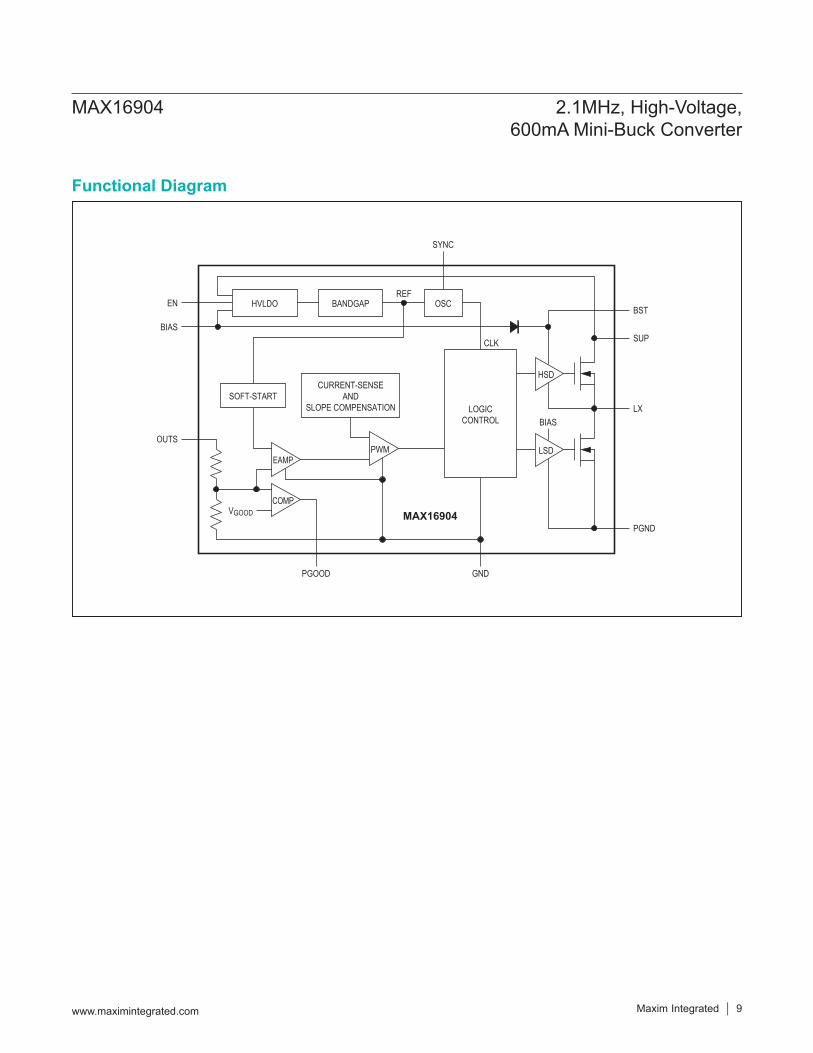
Functional Diagram
MAX16904
LSDPWMEAMP
COMP
HSD
BIASLX
PGND
BST
SUP
LOGICCONTROL
CURRENT-SENSEAND
SLOPE COMPENSATIONSOFT-START
OSCBANDGAP
GND
VGOOD
PGOOD
OUTS
BIAS
HVLDO
SYNC
REFEN
CLK
MAX16904 2.1MHz, High-Voltage,600mA Mini-Buck Converter
www.maximintegrated.com Maxim Integrated 9

Detailed DescriptionThe MAX16904 is a small, current-mode buck converter that features synchronous rectification and requires no external compensation network. The device is designed for 600mA output current, and can stay in dropout by running at 97% duty cycle. It provides an accurate output voltage within the +6.5V to +18V input range. Voltage quality can be monitored by observing the PGOOD signal. The device operates at 2.1MHz (typ) frequency, which allows for small external components, reduced output ripple, and guarantees no AM band interference.The device features an ultra-low 25μA (typ) quiescent supply current in standby mode. Standby mode is entered when load currents are below 5mA and when SYNC is low. The device operates from a +3.5V to +28V supply voltage and tolerates transients up to +42V, making it ideal for automotive applications. The device is available in factory-trimmed output voltages from 1.8V to 10.7V in 100mV steps. Contact the factory for availability of voltage options.
Enable (EN)The device is activated by driving EN high. EN is compat-ible from a +3.3V logic level to automotive battery levels. EN can be controlled by microcontrollers and automotive KEY or CAN inhibit signals. The EN input has no internal pullup/pulldown current to minimize overall quiescent supply current. To realize a programmable undervoltage lockout level, use a resistor-divider from SUP to EN to GND.
BIAS/UVLOThe device features undervoltage lockout. When the device is enabled, an internal bias generator turns on. LX begins switching after VBIAS has exceeded the internal undervoltage lockout level VUVLO = 3V (typ).
Soft-StartThe device features an internal soft-start timer. The output voltage soft-start ramp time is 8ms (typ). If a short circuit or undervoltage is encountered, after the soft-start timer has expired, the device is disabled for 30ms (typ) and it reattempts soft-start again. This pattern repeats until the short circuit has been removed.
Oscillator/Synchronization and Efficiency (SYNC)The device has an on-chip oscillator that provides a switching frequency of 2.1MHz (typ). Depending on the condition of SYNC, two operation modes exist. If SYNC is unconnected or at GND, the device must operate in highly efficient pulse-skipping mode if the load current is below
the SKIP mode current threshold. If SYNC is at BIAS or has a frequency applied to it, the device is in forced PWM mode. The device offers the best of both worlds. The device can be switched during operation between forced PWM mode and SKIP mode by switching SYNC.
SKIP Mode OperationSKIP mode is entered when the SYNC pin is connected to ground or is unconnected and the peak load current is < 350mA (typ). In this mode, the high-side FET is turned on until the current in the inductor is ramped up to 350mA (typ) peak value and the internal feedback voltage is above the regulation voltage (1.2V typ). At this point, both the high-side and low-side FETs are turned off. Depending on the choice of the output capacitor and the load current the high-side FET turns on when OUTS (val-ley) drops below the 1.2V (typ) feedback voltage.
Achieving High Efficiency at Light LoadsThe device operates with very low quiescent current at light loads to enhance efficiency and conserve battery life. When the device enters SKIP mode the output current is monitored to adjust the quiescent current.When the output current is < 5mA, the device operates in the lowest quiescent current mode also called the standby mode. In this mode, the majority of the internal circuitry (excluding that necessary to maintain regulation) in the device, including the internal high-voltage LDO, is turned off to save current. Under no load and with SKIP mode enabled, the device draws only 25μA (typ) current. For load currents > 5mA, the device enters normal SKIP mode while still maintaining very high efficiency.
Controlled EMI with Forced-Fixed FrequencyIn forced PWM mode, the device attempts to operate at a constant switching frequency for all load currents. For tightest frequency control, apply the operating frequency to SYNC. The advantage of this mode is a constant switching frequency, which improves EMI performance; the disadvantage is that considerable current can be thrown away. If the load current during a switching cycle is less than the current flowing through the inductor, the excess current is diverted to GND. With no external load present, the operating current is in the 10mA range.
Extended Input Voltage RangeIn some cases, the device is forced to deviate from its operating frequency independent of the state of SYNC. For input voltages above 18V, the required duty cycle to regulate its output may be smaller than the minimum on-time (80ns, typ). In this event, the device is forced to lower its switching frequency by skipping pulses.
MAX16904 2.1MHz, High-Voltage,600mA Mini-Buck Converter
www.maximintegrated.com Maxim Integrated 10
If the input voltage is reduced and the device approaches dropout, it tries to turn on the high-side FET continu-ously. To maintain gate charge on the high-side FET, the BST capacitor must be periodically recharged. To ensure proper charge on the BST capacitor when in dropout, the high-side FET is turned off every 6.5μs and the low-side FET is turned on for about 150ns. This gives an effective duty cycle of > 97% and a switching frequency of 150kHz when in dropout.
Spread-Spectrum OptionThe device has an optional spread-spectrum version. If this option is selected, then the internal operating frequency varies by +6% relative to the internally generated operat-ing frequency of 2.1MHz (typ). Spread spectrum is offered to improve EMI performance of the device. By varying the frequency 6% only in the positive direction, the device still guarantees that the 2.1MHz frequency does not drop into the AM band limit of 1.8MHz. Additionally, with the low minimum on-time of 80ns (typ) no pulse skipping is observed for a 5V output with 18V input maximum battery voltage in steady state.The internal spread spectrum does not interfere with the external clock applied on the SYNC pin. It is active only when the device is running with internally generated switching frequency.
Power-Good (PGOOD)The device features an open-drain power-good output. PGOOD is an active-high output that pulls low when the output voltage is below 91% of its nominal value. PGOOD is high impedance when the output voltage is above 93% of its nominal value. Connect a 20kΩ (typ) pullup resistor to an external supply or the on-chip BIAS output.
Overcurrent ProtectionThe device limits the peak output current to 1.05A (typ). To protect against short-circuit events, the device shuts off when OUTS is below 1.5V (typ) and one overcurrent event is detected. The device attempts a soft-start restart every 30ms and stays off if the short circuit has not been removed. When the current limit is no longer present, it reaches the output voltage by following the normal soft-start sequence. If the device die reaches the thermal limit of +175°C (typ) during the current-limit event, it immedi-ately shuts off.
Thermal-Overload ProtectionThe device features thermal-overload protection. The device turns off when the junction temperature exceeds +175°C (typ). Once the device cools by 15°C (typ), it turns back on with a soft-start sequence.
Applications InformationInductor SelectionThe nominal inductor value can be calculated using Table based on the nominal output voltage of the device. Select the nearest standard inductance value to the calculated nominal value. The nominal standard value selected should be within ±25% of LNOM for best performance.
Input CapacitorA low-ESR ceramic input capacitor of 1μF or larger is needed for proper device operation. This value may need to be larger based on application input ripple requirements.The discontinuous input current of the buck converter causes large input ripple current. The switching frequency, peak inductor current, and the allowable peak-to-peak input-voltage ripple dictate the input capacitance require-ment. Increasing the switching frequency or the inductor value lowers the peak-to-average current ratio yielding a lower input capacitance requirement.The input ripple comprises mainly of ΔVQ (caused by the capacitor discharge) and ΔVESR (caused by the ESR of the input capacitor). The total voltage ripple is the sum of ΔVQ and ΔVESR. Assume the input-voltage ripple from the ESR and the capacitor discharge is equal to 50% each. The following equations show the ESR and capaci-tor requirement for a target voltage ripple at the input:
Table 1. Inductor Selection
Table 2. Examples for Standard Output Voltages
VOUT (V) LNOM (µH)1.8 to 3.1 VOUT/0.553.2 to 6.5 VOUT/0.966.6 to 8.1 VOUT/1.408.2 to 10 VOUT/1.75
VOUT (V)
CALCULATED LNOM (µH)
STANDARD VALUE (µH)
1.8 3.3 3.33.3 3.4 3.35.0 5.2 4.78.0 5.7 5.6
MAX16904 2.1MHz, High-Voltage,600mA Mini-Buck Converter
www.maximintegrated.com Maxim Integrated 11
ESRP P
OUT
OUTIN
Q SW
VESRII2
I D(1 D)CV f
−
∆=
∆ +
× −=
∆ ×
where:IN OUT OUT
P PIN SW
(V V ) VIV f L−− ×
∆ =× ×
and:OUT
IN
VDV
=
where IOUT is the output current, D is the duty cycle, and fSW is the switching frequency. Use additional input capacitance at lower input voltages to avoid possible undershoot below the UVLO threshold during transient loading.
Output CapacitorTo maintain acceptable phase margin, a minimum ceram-ic output capacitor value of 10μF is needed with a volt-age rating of 2 times the VOUT voltage. Additional output capacitance may be needed based on application-specific output voltage ripple requirements.The allowable output-voltage ripple and the maximum devi-ation of the output voltage during step load currents deter-mine the output capacitance and its ESR. The output ripple comprises of ΔVQ (caused by the capacitor discharge) and ΔVESR (caused by the ESR of the output capacitor). Use low-ESR ceramic or aluminum electrolytic capacitors at the output. For aluminum electrolytic capacitors, the entire output ripple is contributed by ΔVESR. Use the ESROUT equation to calculate the ESR requirement and choose the capacitor accordingly. If using ceramic capacitors, assume the contribution to the output ripple voltage from the ESR and the capacitor discharge to be equal. The following equations show the output capacitance and ESR require-ment for a specified output-voltage ripple.
ESRP P
P POUT
Q SW
VESRIIC
8 V f
−
−
∆=
∆
∆=
× ∆ ×
where:
IN OUT OUTP P
IN SW
OUT_RIPPLE ESR Q
(V V ) VIV f L
V V V
−− ×
∆ =× ×
≅ ∆ + ∆
ΔIP-P is the peak-to-peak inductor current as calculated above and fSW is the converter’s switching frequency. The allowable deviation of the output voltage during fast transient loads also determines the output capacitance and its ESR. The output capacitor supplies the step load current until the converter responds with a greater duty cycle. The response time (tRESPONSE) depends on the closed-loop bandwidth of the converter. The device’s high switching frequency allows for a higher closed-loop bandwidth, thus reducing tRESPONSE and the output capacitance require-ment. The resistive drop across the output capacitor’s ESR and the capacitor discharge causes a voltage droop during a step load. Use a combination of low-ESR tantalum and ceramic capacitors for better transient load and ripple/noise performance. Keep the maximum output-voltage devia-tions below the tolerable limits of the electronics being powered. When using a ceramic capacitor, assume an 80% and 20% contribution from the output capacitance discharge and the ESR drop, respectively. Use the follow-ing equations to calculate the required ESR and capaci-tance value:
ESROUT
STEP
STEP RESPONSEOUT
Q
VESRI
I tCV
∆=
×=
∆
where ISTEP is the load step and tRESPONSE is the response time of the converter. The converter response time depends on the control-loop bandwidth.
PCB Layout GuidelinesCareful PCB layout is critical to achieve low switching power losses and clean stable operation. Use a multilayer board wherever possible for better noise immunity. Refer to the MAX16904 Evaluation Kit for recommended PCB layout. Follow these guidelines for a good PCB layout:1) The input capacitor (4.7μF, see the applications sche-
matic in the Typical Operating Circuits) should be placed right next to the SUP pins (pins 2 and 3 on the TSSOP-EP package). Because the device operates at 2.1MHz switching frequency, this placement is critical for effective decoupling of high-frequency noise from the SUP pins.
MAX16904 2.1MHz, High-Voltage,600mA Mini-Buck Converter
www.maximintegrated.com Maxim Integrated 12
2) Solder the exposed pad to a large copper plane area under the device. To effectively use this copper area as heat exchanger between the PCB and ambient, expose the copper area on the top and bottom side. Add a few small vias or one large via on the copper pad for efficient heat transfer. Connect the exposed pad to PGND ideally at the return terminal of the out-put capacitor.
3) Isolate the power components and high current paths from sensitive analog circuitry.
4) Keep the high current paths short, especially at the ground terminals. The practice is essential for stable jitter-free operation.
5) Connect the PGND and GND together preferably at the return terminal of the output capacitor. Do not con-nect them anywhere else.
6) Keep the power traces and load connections short. This practice is essential for high efficiency. Use thick copper PCB to enhance full load efficiency and power dissipation capability.
7) Route high-speed switching nodes away from sensi-tive analog areas. Use internal PCB layers as PGND to act as EMI shields to keep radiated noise away from the device and analog bypass capacitor.
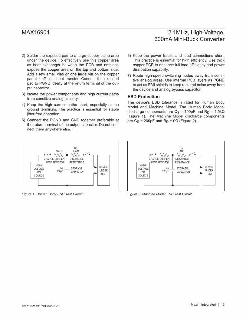
ESD ProtectionThe device’s ESD tolerance is rated for Human Body Model and Machine Model. The Human Body Model discharge components are CS = 100pF and RD = 1.5kΩ (Figure 1). The Machine Model discharge components are CS = 200pF and RD = 0Ω (Figure 2).
Figure 1. Human Body ESD Test Circuit Figure 2. Machine Model ESD Test Circuit
STORAGECAPACITOR
HIGH-VOLTAGE
DCSOURCE
DEVICEUNDERTEST
CHARGE-CURRENT-LIMIT RESISTOR
DISCHARGERESISTANCE
1MΩRD
1.5kΩ
CS100pF
STORAGECAPACITOR
HIGH-VOLTAGE
DCSOURCE
DEVICEUNDERTEST
CHARGE-CURRENT-LIMIT RESISTOR
DISCHARGERESISTANCE
RD0Ω
CS200pF
MAX16904 2.1MHz, High-Voltage,600mA Mini-Buck Converter
www.maximintegrated.com Maxim Integrated 13
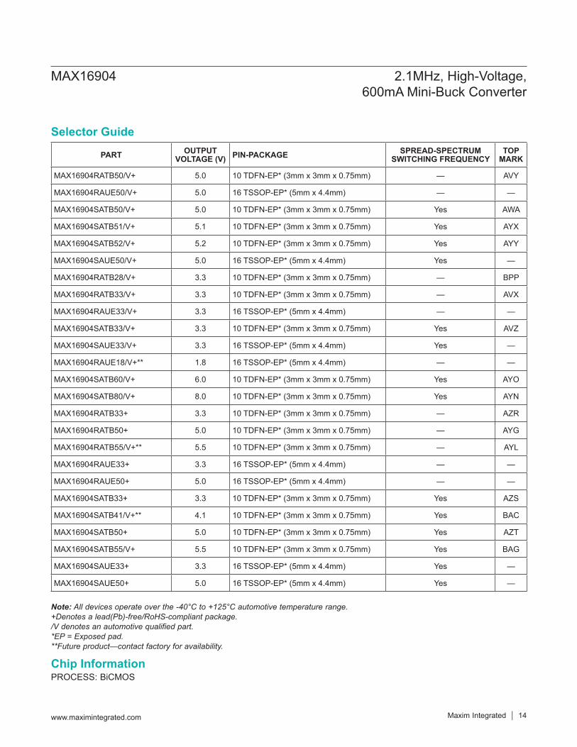
Note: All devices operate over the -40°C to +125°C automotive temperature range.+Denotes a lead(Pb)-free/RoHS-compliant package./V denotes an automotive qualified part.*EP = Exposed pad.**Future product—contact factory for availability.
Selector Guide
Chip InformationPROCESS: BiCMOS
PART OUTPUT VOLTAGE (V) PIN-PACKAGE SPREAD-SPECTRUM
SWITCHING FREQUENCYTOP
MARK
MAX16904RATB50/V+ 5.0 10 TDFN-EP* (3mm x 3mm x 0.75mm) — AVY
MAX16904RAUE50/V+ 5.0 16 TSSOP-EP* (5mm x 4.4mm) — —
MAX16904SATB50/V+ 5.0 10 TDFN-EP* (3mm x 3mm x 0.75mm) Yes AWA
MAX16904SATB51/V+ 5.1 10 TDFN-EP* (3mm x 3mm x 0.75mm) Yes AYX
MAX16904SATB52/V+ 5.2 10 TDFN-EP* (3mm x 3mm x 0.75mm) Yes AYY
MAX16904SAUE50/V+ 5.0 16 TSSOP-EP* (5mm x 4.4mm) Yes —
MAX16904RATB28/V+ 3.3 10 TDFN-EP* (3mm x 3mm x 0.75mm) — BPP
MAX16904RATB33/V+ 3.3 10 TDFN-EP* (3mm x 3mm x 0.75mm) — AVX
MAX16904RAUE33/V+ 3.3 16 TSSOP-EP* (5mm x 4.4mm) — —
MAX16904SATB33/V+ 3.3 10 TDFN-EP* (3mm x 3mm x 0.75mm) Yes AVZ
MAX16904SAUE33/V+ 3.3 16 TSSOP-EP* (5mm x 4.4mm) Yes —
MAX16904RAUE18/V+** 1.8 16 TSSOP-EP* (5mm x 4.4mm) — —
MAX16904SATB60/V+ 6.0 10 TDFN-EP* (3mm x 3mm x 0.75mm) Yes AYO
MAX16904SATB80/V+ 8.0 10 TDFN-EP* (3mm x 3mm x 0.75mm) Yes AYN
MAX16904RATB33+ 3.3 10 TDFN-EP* (3mm x 3mm x 0.75mm) — AZR
MAX16904RATB50+ 5.0 10 TDFN-EP* (3mm x 3mm x 0.75mm) — AYG
MAX16904RATB55/V+** 5.5 10 TDFN-EP* (3mm x 3mm x 0.75mm) — AYL
MAX16904RAUE33+ 3.3 16 TSSOP-EP* (5mm x 4.4mm) — —
MAX16904RAUE50+ 5.0 16 TSSOP-EP* (5mm x 4.4mm) — —
MAX16904SATB33+ 3.3 10 TDFN-EP* (3mm x 3mm x 0.75mm) Yes AZS
MAX16904SATB41/V+** 4.1 10 TDFN-EP* (3mm x 3mm x 0.75mm) Yes BAC
MAX16904SATB50+ 5.0 10 TDFN-EP* (3mm x 3mm x 0.75mm) Yes AZT
MAX16904SATB55/V+ 5.5 10 TDFN-EP* (3mm x 3mm x 0.75mm) Yes BAG
MAX16904SAUE33+ 3.3 16 TSSOP-EP* (5mm x 4.4mm) Yes —
MAX16904SAUE50+ 5.0 16 TSSOP-EP* (5mm x 4.4mm) Yes —
MAX16904 2.1MHz, High-Voltage,600mA Mini-Buck Converter
www.maximintegrated.com Maxim Integrated 14
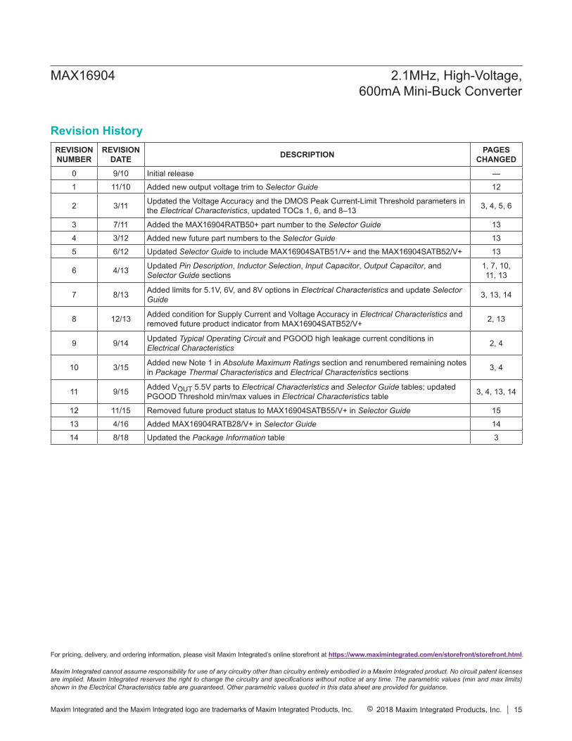
Revision HistoryREVISION NUMBER
REVISION DATE DESCRIPTION PAGES
CHANGED0 9/10 Initial release —1 11/10 Added new output voltage trim to Selector Guide 12
2 3/11 Updated the Voltage Accuracy and the DMOS Peak Current-Limit Threshold parameters in the Electrical Characteristics, updated TOCs 1, 6, and 8–13 3, 4, 5, 6
3 7/11 Added the MAX16904RATB50+ part number to the Selector Guide 134 3/12 Added new future part numbers to the Selector Guide 135 6/12 Updated Selector Guide to include MAX16904SATB51/V+ and the MAX16904SATB52/V+ 13
6 4/13 Updated Pin Description, Inductor Selection, Input Capacitor, Output Capacitor, and Selector Guide sections
1, 7, 10, 11, 13
7 8/13 Added limits for 5.1V, 6V, and 8V options in Electrical Characteristics and update Selector Guide 3, 13, 14
8 12/13 Added condition for Supply Current and Voltage Accuracy in Electrical Characteristics and removed future product indicator from MAX16904SATB52/V+ 2, 13
9 9/14 Updated Typical Operating Circuit and PGOOD high leakage current conditions in Electrical Characteristics 2, 4
10 3/15 Added new Note 1 in Absolute Maximum Ratings section and renumbered remaining notes in Package Thermal Characteristics and Electrical Characteristics sections 3, 4
11 9/15 Added VOUT 5.5V parts to Electrical Characteristics and Selector Guide tables; updated PGOOD Threshold min/max values in Electrical Characteristics table 3, 4, 13, 14
12 11/15 Removed future product status to MAX16904SATB55/V+ in Selector Guide 1513 4/16 Added MAX16904RATB28/V+ in Selector Guide 1414 8/18 Updated the Package Information table 3
Maxim Integrated cannot assume responsibility for use of any circuitry other than circuitry entirely embodied in a Maxim Integrated product. No circuit patent licenses are implied. Maxim Integrated reserves the right to change the circuitry and specifications without notice at any time. The parametric values (min and max limits) shown in the Electrical Characteristics table are guaranteed. Other parametric values quoted in this data sheet are provided for guidance.
Maxim Integrated and the Maxim Integrated logo are trademarks of Maxim Integrated Products, Inc. © 2018 Maxim Integrated Products, Inc. 15
MAX16904 2.1MHz, High-Voltage,600mA Mini-Buck Converter
For pricing, delivery, and ordering information, please visit Maxim Integrated’s online storefront at https://www.maximintegrated.com/en/storefront/storefront.html.