nepp etw 2018: gan hemt power applications: the road to … · 2018-08-15 · epc with freebird...
TRANSCRIPT

GaN HEMT Power Applications: The road to space qualification
Leif ScheickJet Propulsion Laboratory, California Institute of Technology,
Pasadena, CaCopyright 2018 California Institute of Technology. U.S. Government sponsorship
acknowledged. This research was carried out in part by the Jet Propulsion Laboratory, California Institute of Technology, under contract with the National
Aeronautics and Space Administration under the NASA Electronic Parts and Packaging Program (Code AE). Other data was collected from NASA flight projects.

To be presented at the 99h NASA Electronic Parts and Packaging (NEPP) Program Electronic Technology Workshop June 20, 2018, NASA GSFC, Greenbelt, MD.
Program scope
• Working group discusses best methods for evaluating new wide band gap technologies for infusion into space– GRC, JPL, JSC, GSFC, AFRL– Monthly meeting to share data and resources for radiation effects
testing and reliability analyses– Analysis of current commercial efforts
• Previous efforts have been broad stroke testing– Mostly heavy ion testing– Dose effects secondary since GaN HEMT has no oxide– Survey of purchasable devices
• On going and future efforts– Continues radiation testing and analysis– Reliability test screens for new devices– Guidelines for implementation and testing
• All major providers have been tested so…– Deep dive on GaN Systems (E2V), Panasonic (Infineon), EPC
(Freebird Semi)– Pivot to drill down on assurance approaches of “Big Three”– “Keep them honest” testing

To be presented at the 99h NASA Electronic Parts and Packaging (NEPP) Program Electronic Technology Workshop June 20, 2018, NASA GSFC, Greenbelt, MD.
Accomplishments to date
• Have tested four different manufactures• EPC (Gen 1 and 2), GaN Systems, Panasonic and
Transphorm• All have similar failure modes but with many small
differences– Catastrophic SEE associate with drain edge of gate
• Dose effects are secondary since the device has not gate oxide– There are isolation oxides that may contribute– Hydrogen poisoning has been postulated to be a possible
failure mode• Book of knowledge draft is in review and should be
released • EPC Gen 5 devices are in testing this year

To be presented at the 99h NASA Electronic Parts and Packaging (NEPP) Program Electronic Technology Workshop June 20, 2018, NASA GSFC, Greenbelt, MD.
GaN Basics
• Current silicon power solutions are at their innate limits for space applications– Silicon devices are at
efficiency limit– Best hi-rel devices are less
then ~400 V drain-to-source• GaN devices are becoming
available– Reliability effects are a
concern– Gate stress is limited– Thermal effects and aging are
under study at GRC
Dielectric
GaN- - - - - - - - - - - - - - -
Si
AlGaN Electron Generating Layer
DGS- - - -

To be presented at the 99h NASA Electronic Parts and Packaging (NEPP) Program Electronic Technology Workshop June 20, 2018, NASA GSFC, Greenbelt, MD.
RECENT TESTING ACTIVITIES
Panasonic PGA26E19BA, Transporm THX320X, and EPC EPC2046 and EPC2045

To be presented at the 99h NASA Electronic Parts and Packaging (NEPP) Program Electronic Technology Workshop June 20, 2018, NASA GSFC, Greenbelt, MD.
SEE testing with GaN
• GaN devices are very thin (~10 nm) so TAM beamline at 15 MeV/u is fine
• Devices are lateral so angle is an issue
• Most devices have a dead layer of some soft
• Device are tested in static mode so far
To be presented at the 99h NASA Electronic Parts and Packaging (NEPP) Program Electronic Technology Workshop June 20, 2018, NASA GSFC, Greenbelt, MD.
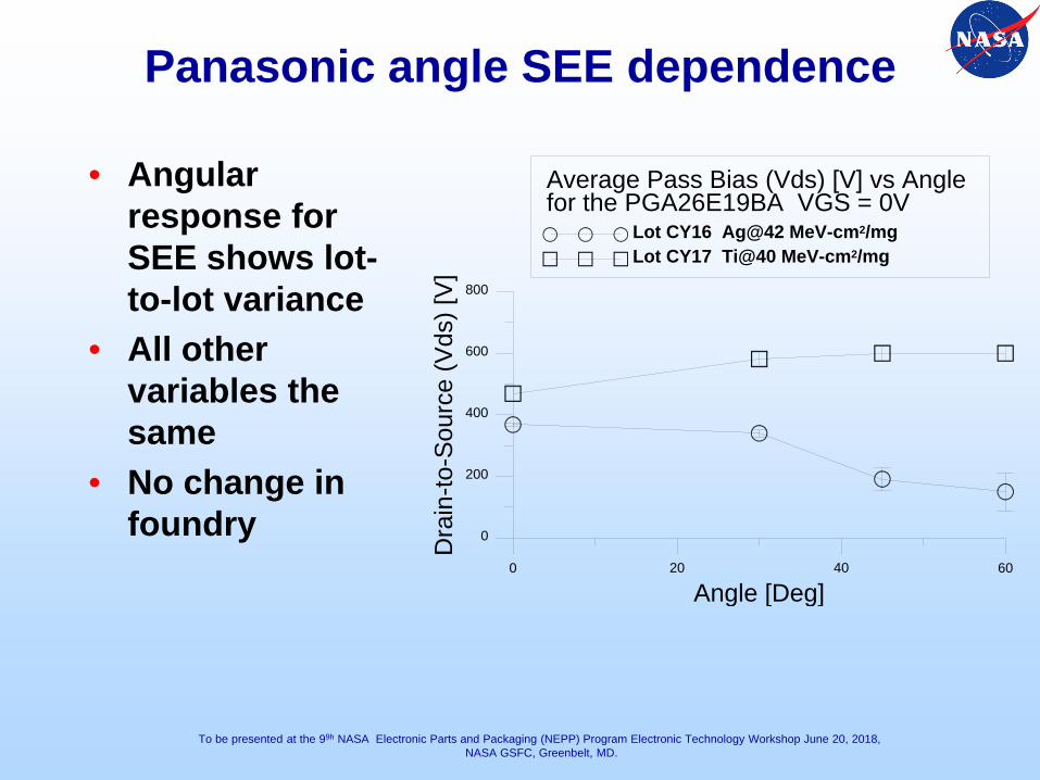
Panasonic angle SEE dependence
• Angular response for SEE shows lot-to-lot variance
• All other variables the same
• No change in foundry
0 20 40 60
Angle [Deg]
0
200
400
600
800
Dra
in-to
-Sou
rce
(Vds
) [V]
Average Pass Bias (Vds) [V] vs Angle for the PGA26E19BA VGS = 0V
Lot CY16 Ag@42 MeV-cm2/mgLot CY17 Ti@40 MeV-cm2/mg

To be presented at the 99h NASA Electronic Parts and Packaging (NEPP) Program Electronic Technology Workshop June 20, 2018, NASA GSFC, Greenbelt, MD.
Effect of gate bias on SEE
• Previous testing show little effect of gate-to-source voltage on Vsee
• Later lots showed similar effect
• This is critical to power applications since negative VGS is used to turn devices off “hard” to meet lower leakages
-8 -6 -4 -2 0
VGS [V]
340
360
380
400
420
440
460
Dra
in-to
-Sou
rce
(Vds
) [V]
Average Pass Bias (Vds) [V]for the PGA26E19BA
VGS=0 V
To be presented at the 99h NASA Electronic Parts and Packaging (NEPP) Program Electronic Technology Workshop June 20, 2018, NASA GSFC, Greenbelt, MD.
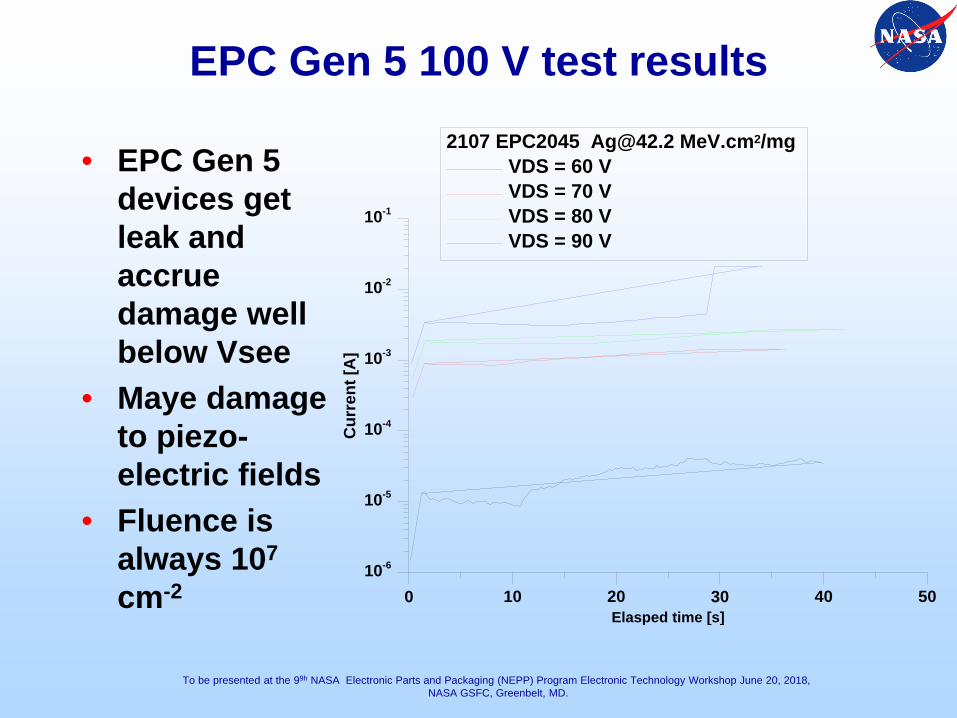
EPC Gen 5 100 V test results
• EPC Gen 5 devices get leak and accrue damage well below Vsee
• Maye damage to piezo-electric fields
• Fluence is always 107
cm-2 0 10 20 30 40 50Elasped time [s]
10-6
10-5
10-4
10-3
10-2
10-1
Cur
rent
[A]
2107 EPC2045 [email protected] MeV.cm2/mg VDS = 60 VVDS = 70 VVDS = 80 VVDS = 90 V

To be presented at the 99h NASA Electronic Parts and Packaging (NEPP) Program Electronic Technology Workshop June 20, 2018, NASA GSFC, Greenbelt, MD.
EPC Gen 5 100 V No beam
• Dry run data with no beam shows no increased leakage
0 20 40 60Elasped time [s]
10-6
10-5
10-4
10-3
10-2
10-1
Cur
rent
[A]
EPC2045 No beam VDS = 100 V

To be presented at the 99h NASA Electronic Parts and Packaging (NEPP) Program Electronic Technology Workshop June 20, 2018, NASA GSFC, Greenbelt, MD.
EPC Gen 5 200 V test results
• EPC Gen 5 devices get leak and accrue damage well below Vsee
• Maybe damage to piezo-electric fields
• Fluence is always 107
cm-2 0 20 40 60Elasped time [s]
10-7
10-6
10-5
10-4
10-3
10-2
10-1
Cur
rent
[A]
0
5
10
15
20
25
Volta
ge [V
]
2123 EPC2046 [email protected] MeV.cm2/mg VDS = 120 VVDS = 140 VVDS = 160 VVDS = 180 V

To be presented at the 99h NASA Electronic Parts and Packaging (NEPP) Program Electronic Technology Workshop June 20, 2018, NASA GSFC, Greenbelt, MD.
EPC Gen 5 200 V test results
• EPC Gen 5 devices get leak and accrue damage well below Vsee
• Maye damage to piezo-electric fields
• Fluence is always 107 cm-2 0 20 40 60
Elasped time [s]
10-6
10-5
10-4
10-3
10-2
10-1
Cur
rent
[A]
0
5
10
15
20
25
Volta
ge [V
]
2126 EPC2046 [email protected] MeV.cm2/mg VDS = 150 VVDS = 160 VVDS = 170 V

To be presented at the 99h NASA Electronic Parts and Packaging (NEPP) Program Electronic Technology Workshop June 20, 2018, NASA GSFC, Greenbelt, MD.
EPC Gen 5 200 V No beam
• Dry run data with no beam shows no increased leakage
0 20 40 60Elasped time [s]
10-7
10-6
10-5
10-4
10-3
10-2
10-1
Cur
rent
[A]
EPC2046 No beam
To be presented at the 99h NASA Electronic Parts and Packaging (NEPP) Program Electronic Technology Workshop June 20, 2018, NASA GSFC, Greenbelt, MD.
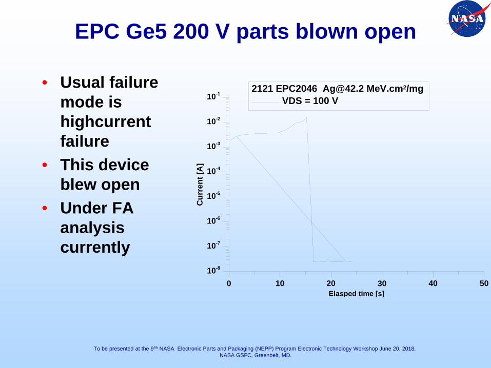
EPC Ge5 200 V parts blown open
• Usual failure mode is highcurrent failure
• This device blew open
• Under FA analysis currently
0 10 20 30 40 50Elasped time [s]
10-8
10-7
10-6
10-5
10-4
10-3
10-2
10-1
Cur
rent
[A]
2121 EPC2046 [email protected] MeV.cm2/mg VDS = 100 V

To be presented at the 99h NASA Electronic Parts and Packaging (NEPP) Program Electronic Technology Workshop June 20, 2018, NASA GSFC, Greenbelt, MD.
Cross section of Vsee
• Cross section is routinely ~2x10⁻⁶ cm2
• This is approximately the area of the drain edge of the gate
15 20 25 30 35 40 45
LET [MeV.cm2/mg]
10-7
10-6
Cro
ss S
ectio
n [c
m2 ]
Cross section vs LETEPC2045 VGS = 0 VEPC2046 VGS = 0 V

To be presented at the 99h NASA Electronic Parts and Packaging (NEPP) Program Electronic Technology Workshop June 20, 2018, NASA GSFC, Greenbelt, MD.
Vsee dependence on LET
• Two hundred volt rated parts are more sensitive to SEE
• Similar behavior to Gen 1 and Gen 2
15 20 25 30 35 40 45
LET [MeV.cm2/mg]
40
80
120
160
200
Cro
ss S
ectio
n [c
m2 ]
Survival Voltage vs LETEPC2045 VGS = 0 VEPC2046 VGS = 0 V

To be presented at the 99h NASA Electronic Parts and Packaging (NEPP) Program Electronic Technology Workshop June 20, 2018, NASA GSFC, Greenbelt, MD.
COMMERCIAL QUALIFICATION EFFORTS

To be presented at the 99h NASA Electronic Parts and Packaging (NEPP) Program Electronic Technology Workshop June 20, 2018, NASA GSFC, Greenbelt, MD.
Reviewing the “Big Three”
• Three entities have emerged to sate the appetite for GaN power system applications
• GaN Systems with E2V, Panasonic with Infineon, EPC with Freebird Semiconductor
• All three rushing to “fill the gaps” on qualification – radiation, reliability and packaging
• EEE part qualification is almost exclusively based on silicon “lessons learned”– MIL-PRF-19500, MIL-PRF-38584, MIL-PRF-38535
• Using these as a basis of GaN qualification overlooks possible escapes– E.g.: Current collapse, dynamic RDSon, channel hot
carrier stress, inverse piezoelectric effect, electromigration
To be presented at the 99h NASA Electronic Parts and Packaging (NEPP) Program Electronic Technology Workshop June 20, 2018, NASA GSFC, Greenbelt, MD.
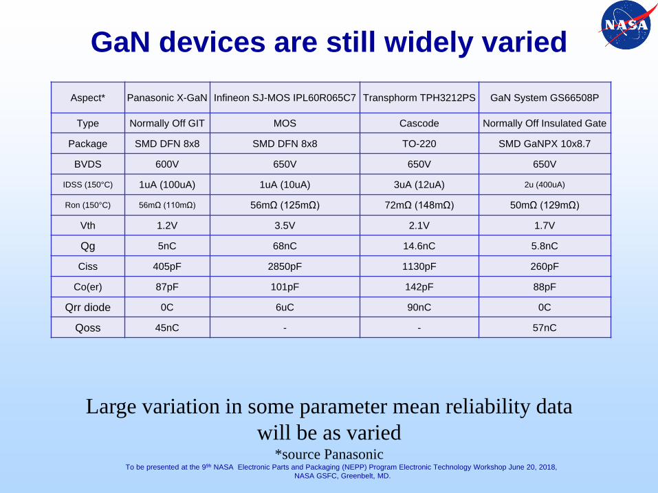
GaN devices are still widely variedAspect* Panasonic X-GaN Infineon SJ-MOS IPL60R065C7 Transphorm TPH3212PS GaN System GS66508P
Type Normally Off GIT MOS Cascode Normally Off Insulated Gate
Package SMD DFN 8x8 SMD DFN 8x8 TO-220 SMD GaNPX 10x8.7
BVDS 600V 650V 650V 650V
IDSS (150°C) 1uA (100uA) 1uA (10uA) 3uA (12uA) 2u (400uA)
Ron (150°C) 56mΩ (110mΩ) 56mΩ (125mΩ) 72mΩ (148mΩ) 50mΩ (129mΩ)
Vth 1.2V 3.5V 2.1V 1.7V
Qg 5nC 68nC 14.6nC 5.8nC
Ciss 405pF 2850pF 1130pF 260pF
Co(er) 87pF 101pF 142pF 88pF
Qrr diode 0C 6uC 90nC 0C
Qoss 45nC - - 57nC
Large variation in some parameter mean reliability data will be as varied
*source Panasonic

To be presented at the 99h NASA Electronic Parts and Packaging (NEPP) Program Electronic Technology Workshop June 20, 2018, NASA GSFC, Greenbelt, MD.
MIL-STD-19500 is extensive
• The initial urge is to use 19500 as the standard for qualification– MIL-STD-883 is also used
• Followed by MIL-STD-750 TM1019 and 1080 for radiation
• Proper qualification needs to identify the gaps
MIL-STD-750 Sub JANTX, JANTXV JANTX, JANTXVJANTX JANTXV JANS Method Group Large Lot Small Lot
Internal visual inspection (precap) - 100% 100% 2073, 2074, 2072 Quantity QuantityTemperature cycling (temp. cycle) (accept number) (accept number)
20 cycles > 10 minutes @ Solderability 15 leads (0) 4 leads (0)
temperature extremesResistance to
solvents15 (0) 3 (0)
Thermal impedance 100% 100% 100% 3161, 3101, 3103 Temperature cycling
Constant acceleration 20kG or 10kG > 10W - - 100% 2006(45 cycles, including
screening)
Particle impact noise detection 2052Thermal shock (10
cycles)
(PIND - devices with internal cav.) Condition AHermetic seal (fine
and gross leak)
Serialization of devices - - 100%Electrical
measurements
100%Steady state op. life
or
R&R intermittent op. life
High temperature gate bias 100% 100% 100% 1042Electrical
measurements(within x hrs) Condition B Bond strength 11 wires (0) 11 wires (0)
MOSFETs/IGBTs: (48 hrs) (48 hrs) (48 hrs) 4 Decap internal visual 1 (0) 1 (0)
Interim electrical 100% 100% 100% 5Thermal resistance (Performed 100%)
15 (0) 6 (0)
and delta parametersHigh temperature
life (340 hours) non-operating*
(within x hrs) (24 hrs) (24 hrs) (16 hrs)Electrical
measurementsHigh temperature reverse bias
(hours minimum)MOSFETs/IGBTs: 100% 100% 100% 1042
(160 hrs) (160 hrs) (240 hrs) Condition ADiodes: 100% 100% 100% 1038
(96 hrs) (96 hrs) (240 hrs) Condition AFinal electrical test Sub All Quality Levels All Quality Levels
and delta parameters Group Large Lot Small LotHermetic seal (fine and gross leak) 100% 100% 100% 1071 Quantity Quantity
Radiography - - 100% 2076 (accept number) (accept number)External visual exam 1 Physical dimensions 15 (0) 6 (0)
(after complete marking) Thermal shockCase Isolation Terminal strength
(Case Isolated Packages)Hermetic seal (fine
and gross leak)Moisture resistance
Electrical measurements
ShockVibration, variable
frequencyConstant
accelerationElectrical
measurements4 Salt atmosphere
(corrosion)15 (0) 6 (0)
Sub JANS JANTX, JANTXV 5 N/A
Group Quantity QuantitySteady state op. life
or
(accept number) (accept number)intermittent op. life
or blocking life
1 Visual and mechanical inspection 15 (0) 45 (0)Electrical
measurements
2 DC (static) test at +25°C 7 Internal water vapor 3 (0) 3 (0)
3 DC (static) tests at max. and min. temps.4 Dynamic tests at +25°C
Safe operating area test (power trans.): a. DC
b. Clamped inductive c. Unclamped inductive Sub JANTXV JANS Wafer
End point electrical measurements Group Inspection Lot Inspection LotSurge current (diodes and rectifiers) Quantity QuantityEnd point electrical measurements (accept number) (accept number)
7 Selected static and dynamic testsSteady-state total dose irradiation
4 (0) See note 1.2 (0) See note 2.1 (0) See note 3.4 (0) See note 1.2 (0) See note 2.
Sub JANS, Large Lot JANS, Small Lot 1 (0) See note 3.Group Quantity Quantity
(accept number) (accept number)1 Physical dimensions 22 (0) 8 (0)
Solderability 15 leads (0) 6 leads (0)Resistance to solvents 15 (0) 6 (0)
Temperature cycling (100 cycles)Surge (diodes only)
Hermetic seal (fine and gross leak)Electrical measurements Sub All Quality Levels
Decap internal visual 6 (0) 6 (0) Group QuantityBond strength 22 wires (0) or 11 (0) 12 wires (0) or 6 (0) (accept number)
SEM (when specified)* 6 (0)Thermal shock (100
cycles)Die shear 11 (0) 6 (0) or
Intermittent op. lifeTemp. cycling (500
cycles min.)
Electrical measurementsElectrical
MeasurementsAccelerated HTRB (120 hours) Steady state op. life
Electrical measurementsElectrical
measurementsAccelerated HTGB (24 hrs) 4 Thermal resistance 22 (0)
Electrical measurements Barometric pressure
Bond strength 22 wires (0) 20 wires (0)(derives with rated
voltage > 200V6 Thermal resistance 22 (0) 12 (0) 6 ESD 3 (0)
High Temp Life (340 Hours Non-Operating)Electrical
1051
- - 100%
Interim electrical parameters - -
Test/Inspection Screening Level
100% 100% 100%
- - 100% 2071
100% 100% 100% 1081
100% 100% 100%
22 (0) 12 (0)
Parameters
116 (0) 116 (0)
5
45 (0)
45 (0)
622 (0)
2
22 (0) 6 (0)
Parameters
1
2
22 (0) 6 (0)
3
45 (0) 12 (0)
Parameters
1 per MIL-PRF-19500
2 per MIL-PRF-19500
5 15 (0)
Parameters
2
Qualification 11 (0)
CI 11 (0)MIL-PRF-19500 Group B InspectionMechanical Verification (JANS)
*Note: Not applicable for Schottky's
MIL-PRF-19500 Group B InspectionMIL-PRF-19500 Screening Requirements
MIL-PRF-19500 Quality Conformance Inspection
MIL-PRF-19500 Group A InspectionElectrical Verification
5
22 (0) 12 (0)
7
32 (0) 12 (0)
Parameters
2
3
22 (0) 6 (0)
4
MIL-PRF-19500 Group E InspectionPackage Qualification
MIL-PRF-19500 Group D InspectionRadiation Hardness Assurance Program
1. For device types ≥ 4,000 die per wafer2. For device types > 500 and < 4,000 die per wafer3. For device types ≤ 500 die per wafer
Mechanical Verification(JANTX, JANTXV)
*Note: Not applicable for power MOSFETs
MIL-PRF-19500 Group C InspectionLong-term Reliability Verification
3
22 (0) 6 (0)
6
22 (0) 12 (0)
6
32 (0) 12 (0)
Parameters

To be presented at the 99h NASA Electronic Parts and Packaging (NEPP) Program Electronic Technology Workshop June 20, 2018, NASA GSFC, Greenbelt, MD.
Birds eye view
Manufacturer Reliability flow
Relibity TM RHA reference
GapAnalysis
Panasonic Own Own None Case-by-case
Freebird(EPC)
MIL-PRF-19500
MIL-STD-750 MIL-STD-750 Case-by-case
E2V (GaNSystems)
Own MIL-STD-883 5011, etc
Own Case-by-case
Qualification efforts vary widely between vendors“Secret sauce” requires NDAs to reveal process
Concern is fixing one issue (e.g., current collapse) will result in a new failure mode!

To be presented at the 99h NASA Electronic Parts and Packaging (NEPP) Program Electronic Technology Workshop June 20, 2018, NASA GSFC, Greenbelt, MD.
NASA QUALIFICATION GUIDELINE

To be presented at the 99h NASA Electronic Parts and Packaging (NEPP) Program Electronic Technology Workshop June 20, 2018, NASA GSFC, Greenbelt, MD.
Radiation qualification
• What we know so far– SEE risk associated with the drain edge of the gate in higher bias– Total dose risk is minimal
• What we need to know to have an efficient testing campaign– What temperature is worst case for SEE testing?– What are the latent damage effects of ion testing? – What is the best approach for PIGS and PIDS testing?– What is the effect of burn-in on the testing?– Is there a synergistic effect between dose and SEE?– What is the worst case ion condition for SEE testing?– Does gate stress exacerbate dose or ion effects?– What is worst case – static or dynamic? – What is the effect of dynamic RDSon on dose or SEE effects?– Are there any device specifications that could indicate radiation
effects?• Until these trends are analytically known
– Test early and test often

To be presented at the 99h NASA Electronic Parts and Packaging (NEPP) Program Electronic Technology Workshop June 20, 2018, NASA GSFC, Greenbelt, MD.
Case in point – three difference manufactures
Dielectric
GaN- - - - - - - - - - - - - - -
Si
AlGaN Electron Generating Layer
DGS- - - -
In contrast, silicon power MOSFETs almost all look the same

To be presented at the 99h NASA Electronic Parts and Packaging (NEPP) Program Electronic Technology Workshop June 20, 2018, NASA GSFC, Greenbelt, MD.
Future work
• More testing – Panasonic parts– Transphorm– EPC Gen 5
• Testing guideline– Modeling data is the best bet
• Leverage off flight projects– Power design engineers can’t take there eyes off of the
efficiency number