overview - college of engineering | umass amherst · tmr0 register overflow, rb port change and...
TRANSCRIPT

Overview Lab Assignment 2
— Learning how to use interrupts.
— Interfacing to an external bus.
— State machines in a PLD.
— Data handshaking.
— Moving towards a full system.
1

Tasks to be Completed Lab Assignment 2
— Improve on Lab 1
� Efficient printing of character strings
� Program Timer 0.
— Interface 7032 PLDs to 16F877.
— one switch attached to PLD input
— four LEDs attached to PLD output.
— 16F877 reads switch inputs, write LEDs
— Four bit counter created inside PLD.
— Value echoed to terminal if switch value changes.
2
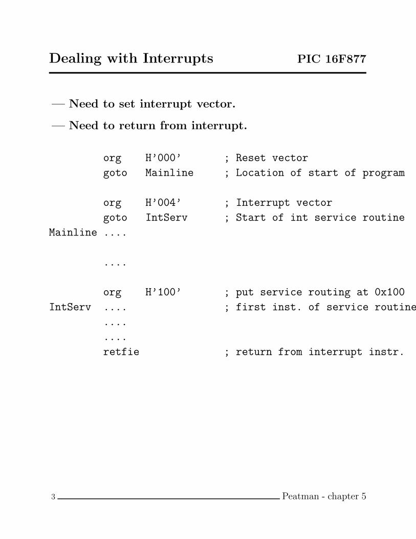
Dealing with Interrupts PIC 16F877
— Need to set interrupt vector.
— Need to return from interrupt.
org H’000’ ; Reset vector
goto Mainline ; Location of start of program
org H’004’ ; Interrupt vector
goto IntServ ; Start of int service routine
Mainline ....
....
org H’100’ ; put service routing at 0x100
IntServ .... ; first inst. of service routine
....
....
retfie ; return from interrupt instr.
3 Peatman - chapter 5
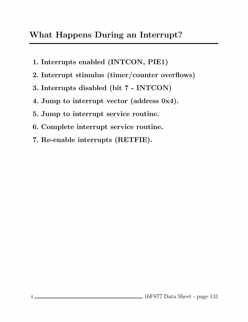
What Happens During an Interrupt?
1. Interrupts enabled (INTCON, PIE1)
2. Interrupt stimulus (timer/counter overflows)
3. Interrupts disabled (bit 7 - INTCON)
4. Jump to interrupt vector (address 0x4).
5. Jump to interrupt service routine.
6. Complete interrupt service routine.
7. Re-enable interrupts (RETFIE).
4 16F877 Data Sheet - page 131

INTCON Register PIC 16F877
PIC16F87X
DS30292B-page 20 1999 Microchip Technology Inc.
2.2.2.3 INTCON REGISTER
The INTCON Register is a readable and writable regis-ter, which contains various enable and flag bits for theTMR0 register overflow, RB Port change and ExternalRB0/INT pin interrupts.
REGISTER 2-3: INTCON REGISTER (ADDRESS 0Bh, 8Bh, 10Bh, 18Bh)
Note: Interrupt flag bits get set when an interruptcondition occurs, regardless of the state ofits corresponding enable bit or the globalenable bit, GIE (INTCON<7>). User soft-ware should ensure the appropriate inter-rupt flag bits are clear prior to enabling aninterrupt.
R/W-0 R/W-0 R/W-0 R/W-0 R/W-0 R/W-0 R/W-0 R/W-x
GIE PEIE T0IE INTE RBIE T0IF INTF RBIF R = Readable bitW = Writable bitU = Unimplemented bit,
read as ‘0’- n= Value at POR reset
bit7 bit0
bit 7: GIE: Global Interrupt Enable bit1 = Enables all un-masked interrupts0 = Disables all interrupts
bit 6: PEIE: Peripheral Interrupt Enable bit1 = Enables all un-masked peripheral interrupts0 = Disables all peripheral interrupts
bit 5: T0IE: TMR0 Overflow Interrupt Enable bit1 = Enables the TMR0 interrupt0 = Disables the TMR0 interrupt
bit 4: INTE: RB0/INT External Interrupt Enable bit1 = Enables the RB0/INT external interrupt0 = Disables the RB0/INT external interrupt
bit 3: RBIE: RB Port Change Interrupt Enable bit1 = Enables the RB port change interrupt0 = Disables the RB port change interrupt
bit 2: T0IF: TMR0 Overflow Interrupt Flag bit1 = TMR0 register has overflowed (must be cleared in software)0 = TMR0 register did not overflow
bit 1: INTF: RB0/INT External Interrupt Flag bit1 = The RB0/INT external interrupt occurred (must be cleared in software)0 = The RB0/INT external interrupt did not occur
bit 0: RBIF: RB Port Change Interrupt Flag bit1 = At least one of the RB7:RB4 pins changed state (must be cleared in software)0 = None of the RB7:RB4 pins have changed state
5 16F877 Data Sheet - page 20

PIE1 PIC 16F877
1999 Microchip Technology Inc. DS30292B-page 21
PIC16F87X
2.2.2.4 PIE1 REGISTER
The PIE1 register contains the individual enable bits forthe peripheral interrupts.
REGISTER 2-4: PIE1 REGISTER (ADDRESS 8Ch)
Note: Bit PEIE (INTCON<6>) must be set toenable any peripheral interrupt.
R/W-0 R/W-0 R/W-0 R/W-0 R/W-0 R/W-0 R/W-0 R/W-0
PSPIE(1) ADIE RCIE TXIE SSPIE CCP1IE TMR2IE TMR1IE R = Readable bitW = Writable bitU = Unimplemented bit,
read as ‘0’- n= Value at POR reset
bit7 bit0
bit 7: PSPIE(1): Parallel Slave Port Read/Write Interrupt Enable bit1 = Enables the PSP read/write interrupt0 = Disables the PSP read/write interrupt
bit 6: ADIE: A/D Converter Interrupt Enable bit1 = Enables the A/D converter interrupt0 = Disables the A/D converter interrupt
bit 5: RCIE: USART Receive Interrupt Enable bit1 = Enables the USART receive interrupt0 = Disables the USART receive interrupt
bit 4: TXIE: USART Transmit Interrupt Enable bit1 = Enables the USART transmit interrupt0 = Disables the USART transmit interrupt
bit 3: SSPIE: Synchronous Serial Port Interrupt Enable bit1 = Enables the SSP interrupt0 = Disables the SSP interrupt
bit 2: CCP1IE: CCP1 Interrupt Enable bit1 = Enables the CCP1 interrupt0 = Disables the CCP1 interrupt
bit 1: TMR2IE: TMR2 to PR2 Match Interrupt Enable bit1 = Enables the TMR2 to PR2 match interrupt0 = Disables the TMR2 to PR2 match interrupt
bit 0: TMR1IE: TMR1 Overflow Interrupt Enable bit1 = Enables the TMR1 overflow interrupt0 = Disables the TMR1 overflow interrupt
Note 1: PSPIE is reserved on 28-pin devices; always maintain this bit clear.
6 16F877 Data Sheet - page 21
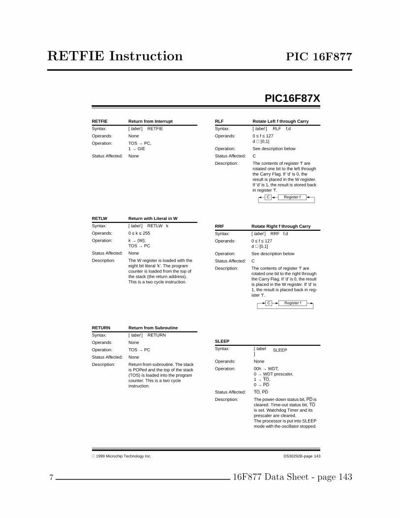
RETFIE Instruction PIC 16F877
1999 Microchip Technology Inc. DS30292B-page 143
PIC16F87X
RETFIE Return from Interrupt
Syntax: [ label ] RETFIE
Operands: None
Operation: TOS → PC,1 → GIE
Status Affected: None
RETLW Return with Literal in W
Syntax: [ label ] RETLW k
Operands: 0 ≤ k ≤ 255
Operation: k → (W); TOS → PC
Status Affected: None
Description: The W register is loaded with the eight bit literal ’k’. The program counter is loaded from the top of the stack (the return address). This is a two cycle instruction.
RETURN Return from Subroutine
Syntax: [ label ] RETURN
Operands: None
Operation: TOS → PC
Status Affected: None
Description: Return from subroutine. The stack is POPed and the top of the stack (TOS) is loaded into the program counter. This is a two cycle instruction.
RLF Rotate Left f through Carry
Syntax: [ label ] RLF f,d
Operands: 0 ≤ f ≤ 127d ∈ [0,1]
Operation: See description below
Status Affected: C
Description: The contents of register ’f’ are rotated one bit to the left through the Carry Flag. If ’d’ is 0, the result is placed in the W register. If ’d’ is 1, the result is stored back in register ’f’.
RRF Rotate Right f through Carry
Syntax: [ label ] RRF f,d
Operands: 0 ≤ f ≤ 127d ∈ [0,1]
Operation: See description below
Status Affected: C
Description: The contents of register ’f’ are rotated one bit to the right through the Carry Flag. If ’d’ is 0, the result is placed in the W register. If ’d’ is 1, the result is placed back in reg-ister ’f’.
SLEEP
Syntax: [ label ]
SLEEP
Operands: None
Operation: 00h → WDT,0 → WDT prescaler,1 → TO,0 → PD
Status Affected: TO, PD
Description: The power-down status bit, PD is cleared. Time-out status bit, TO is set. Watchdog Timer and its prescaler are cleared.The processor is put into SLEEP mode with the oscillator stopped.
Register fC
Register fC
7 16F877 Data Sheet - page 143

Timer0 Interrupt PIC 16F877
1999 Microchip Technology Inc. DS30292B-page 47
PIC16F87X
5.0 TIMER0 MODULEThe Timer0 module timer/counter has the following fea-tures:
• 8-bit timer/counter• Readable and writable
• 8-bit software programmable prescaler• Internal or external clock select• Interrupt on overflow from FFh to 00h
• Edge select for external clock
Figure 5-1 is a block diagram of the Timer0 module andthe prescaler shared with the WDT.
Additional information on the Timer0 module is availablein the PICmicro™ Mid-Range MCU Family ReferenceManual (DS33023).
Timer mode is selected by clearing bit T0CS(OPTION_REG<5>). In timer mode, the Timer0 mod-ule will increment every instruction cycle (without pres-caler). If the TMR0 register is written, the increment isinhibited for the following two instruction cycles. Theuser can work around this by writing an adjusted valueto the TMR0 register.
Counter mode is selected by setting bit T0CS(OPTION_REG<5>). In counter mode, Timer0 willincrement either on every rising or falling edge of pinRA4/T0CKI. The incrementing edge is determined bythe Timer0 Source Edge Select bit T0SE(OPTION_REG<4>). Clearing bit T0SE selects the ris-ing edge. Restrictions on the external clock input arediscussed in detail in Section 5.2.
The prescaler is mutually exclusively shared betweenthe Timer0 module and the watchdog timer. The pres-caler is not readable or writable. Section 5.3 details theoperation of the prescaler.
5.1 Timer0 Interrupt
The TMR0 interrupt is generated when the TMR0 reg-ister overflows from FFh to 00h. This overflow sets bitT0IF (INTCON<2>). The interrupt can be masked byclearing bit T0IE (INTCON<5>). Bit T0IF must becleared in software by the Timer0 module interrupt ser-vice routine before re-enabling this interrupt. TheTMR0 interrupt cannot awaken the processor fromSLEEP since the timer is shut off during SLEEP.
FIGURE 5-1: BLOCK DIAGRAM OF THE TIMER0/WDT PRESCALER
RA4/T0CKI
T0SE
Pin
MUX
CLKOUT (= FOSC/4)
SYNC2
CyclesTMR0 reg
8-bit Prescaler
8 - to - 1MUX
MUX
M U X
WatchdogTimer
PSA
0 1
0
1
WDTTime-out
PS2:PS0
8
Note: T0CS, T0SE, PSA, PS2:PS0 are (OPTION_REG<5:0>).
PSA
WDT Enable bit
MUX
0
1 0
1
Data Bus
Set Flag Bit T0IFon Overflow
8
PSAT0CS
PRESCALER
8 16F877 Data Sheet - page 47-49

Using Timer0 Interrupt PIC 16F877
— Initialize timer 0 to overflow about every
.0327 seconds.
� See example on page 100 of Peatman.
— Force interrupt when counter overflows.
— When interrupt occurs, toggle Port C, bit 2.
— Be sure to initialize appropriate registers.
9 Peatman - pages 100-103

Data Exchange with a PLD PIC 16F877
— Goal: Use ports A, B, C, D to exchange data with
PLD.
— Port A - four bit address value.
— Port B - four bit data input.
— Port C - up to six control signals.
— Port D - four bit data output.
— Create a four-bit write and read transaction.
— Transfer should be robust.
10

Data Exchange with a PLD PIC 16F877
— Valid signals indicate when data transfer occurs.
— Four bit address followed by data.
— For a PIC write, PIC must wait for acknowledge.
— For a PIC read, PLD must wait for data
acknowledge.
— Use 4MHz clock for both PIC and PLD.
— Show handshaking signals on logic analyzer.
11 Altera data book

Example: Control Signals Port C
— Configure port C data direction register.
— PIC data valid/EPLD data accept (PICSTROBE)
Port C output.
— PIC data accept/EPLD data valid (PLDSTROBE)
Port C input.
— PIC Read/Write signal (R/W )
Port C output.
— Could use other encodings.
12

Inside/Outside the EPLD
— Interface 12 address/data + control signals to PIC.
— One switch input into PLD.
— Four LED outputs from PLD.
— Four bit internal register.
— Address and R/W used to select
destination.
13 Altera 7032 data sheet

Example: Write Transaction 16F877
After port A, B, C, D initialization:
1. Send address to Port A.
2. Set R/W signal to read.
3. Assert PICREADY signal.
4. Sample PLDREADY to see if PLD has address.
5. When PLDREADY asserted, deassert
PICREADY.
6. Wait for PLDREADY deasserted.
7. Repeat previous six steps with data on Port D.
14

Example: Read Transaction 16F877
After port A, B, C, D initialization:
— Similar address transaction as write.
— Read value from EPLD to port B.
— Follow sequential rules.
— Data shouldn’t be overwritten.
— Can be simulated with MPSIM
15

PLD State Machine Suggestions 16F877
— Implement using VHDL.
— One state machine to check/fetch addresses.
� check PICREADY.
� assert/deassert PLDREADY
— One state machine for READ transactions:
� Decode address.
� Enable correct location (switches, register)
� Assert data to Port B.
— One state machine for WRITE transactions:
� Decode address.
� Enable correct location (LEDs, register)
� Read data from Port D to correct location.
16

Displaying Character Strings PIC 16F877
— Need to display a string of characters.
— Consider printing string “wow”
call wait ; subroutine which checks PIR bit 4.
movlw ’w’ ; send ASCII w char. to W
movwf TXREG ; send w char. to UART trans. buffer
call wait ; subroutine which checks PIR bit 4.
movlw ’o’ ; send ASCII o char. to W
movwf TXREG ; send o char. to UART trans. buffer
call wait ; subroutine which checks PIR bit 4.
movlw ’w’ ; send ASCII w char. to W
movwf TXREG ; send w char. to UART trans. buffer
— Approach is clumsy, verbose.
17 Peatman - section 8.7

Displaying Character Strings PIC 16F877
— Before introducing the new approach, consider this
code.
ORG 0x0
goto Start ; jump to the start of the program
ORG 0x5
sub1 nop ; start of a subroutine
.
.
return ; return from subroutine
ORG 0x30
Start .
.
.
call sub1 ; call the routine
nop ; first instr. after return
— When call is executed the following happens:
1. PC receives address of sub1
2. top of stack (TOS) receives return addr.
18 Peatman - section 8.7

Displaying Character Strings PIC 16F877
— When return is executed the following happens:
1. PC receives top of stack (TOS), the return
address.
— Consider a new instruction RETLW k
— When retlw is executed the following happens:
1. PC receives top of stack (TOS), the return
address.
2. The constant value k is placed in the
W register
— What if the k value was a character?
19 Peatman - section 8.7

Character String Program PIC 16F877
BANK0RAM EQU H’20’ ; equate a constant to hex 20.
ORG BANK0RAM ; reserve space in DATA MEMORY
cblock ; create a pointer in bank 0 at location 20
POINTER ; name of value
endc
ORG 0x0
goto Start ; jump to the start of the program
ORG 0x5
sub1 movf POINTER, W ; move value in POINTER to W
addwf PCL, F ; add value to PC
retlw A’w’
retlw A’o
retlw A’w’
retlw 0
RETURN ; shouldn’t get here
ORG 0x30
Start clrf POINTER
Loop call sub1
. ; check if return value is 0
btfsc status, z ; branch if not 0
goto Done ; else done
. ; check bit 4 in PIR
movwf TXREG
. ; increment POINTER
goto Loop ; print another character
ORG 0x60
Done nop
goto Done
20 Peatman - page 49

Displaying Character Strings PIC 16F877
— Possible to replace numerous RETLW instructions
with dt directive.
21 Peatman - page 155

Using Macros Lab 2 Hints
Bank0 MACRO ; macro to select bank 0
bcf STATUS, RP0
bcf STATUS, RP1
ENDM
— Make 16F877 macros for read/write transactions.
— Macros are expanded by assembler.
— Later changes can be confined to macro.
22
Demonstration Lab 2
— Rewire lab kit for lab two (PLD, clock)
— Implement using VHDL.
— Demonstrate using logic analyzer.
— Implement serial interface using constant strings.
— Implement timer 0 interrupt and LED toggle.
23

Suggestions Lab 2
— Check write transaction first.
— Look at signals on analyzer.
— Debug read transaction.
— Get interrupts with timer working.
— Get constant string code working.
— Demonstrate working system.
24

Reading Lab 2
— Peatman - chapter 5
— Peatman - pages 100-103
— Peatman - section 8.7 (skim)
— 16F877 data sheet - pages 46-49
— 16F877 data sheet - pages 131-133
— 16F877 data sheet - pages 20-21
— Altera 7032 data sheet
25

Summary Lab 2
— Display constant strings using directive dt.
— Program counter to toggle LED with interrupts.
— Implement bus transaction with PLD.
— VHDL state machines in PLD to handle data
transfer.
— Logic analyzer usage.
26