pic16ce62x - farnell.com · rb0/int rb1 rb2 ra4/t0cki pic16ce62x rb3 dd ... timer module(s) tmr0...
TRANSCRIPT

OTP 8-Bit CMOS MCU with EEPROM Data Memory
PIC16CE62X
62X.bk Page 1 Tuesday, March 10, 1998 3:40 PM
Devices included in this data sheet:
• PIC16CE623• PIC16CE624• PIC16CE625
High Performance RISC CPU:
• Only 35 instructions to learn• All single-cycle instructions (200 ns), except for
program branches which are two-cycle• Operating speed:
- DC - 20 MHz clock input- DC - 200 ns instruction cycle
• Interrupt capability• 16 special function hardware registers• 8-level deep hardware stack• Direct, Indirect and Relative addressing modes
Peripheral Features:
• 13 I/O pins with individual direction control• High current sink/source for direct LED drive• Analog comparator module with:
- Two analog comparators- Programmable on-chip voltage reference
(VREF) module- Programmable input multiplexing from device
inputs and internal voltage reference- Comparator outputs can be output signals
• Timer0: 8-bit timer/counter with 8-bit programmable prescaler
Special Microcontroller Features:
• In-Circuit Serial Programming (ICSP™) (via two pins)
• Power-on Reset (POR)• Power-up Timer (PWRT) and Oscillator Start-up
Timer (OST)• Brown-out Reset• Watchdog Timer (WDT) with its own on-chip RC
oscillator for reliable operation
Device Program Memory
RAM Data
Memory
EEPROM Data
Memory
PIC16CE623 512x14 96x8 128x8
PIC16CE624 1Kx14 96x8 128x8
PIC16CE625 2Kx14 128x8 128x8
1998 Microchip Technology Inc. Prelimin
Pin Diagrams
Special Microcontroller Features (cont’d)
• 1,000,000 erase/write cycle EEPROM data mem-ory
• EEPROM data retention > 40 years• Programmable code protection• Power saving SLEEP mode• Selectable oscillator options• Four user programmable ID locations
CMOS Technology:
• Low-power, high-speed CMOS EPROM/EEPROM technology
• Fully static design• Wide operating voltage range
- 3.0V to 5.5V• Commercial, industrial and extended tempera-
ture range• Low power consumption
- < 2.0 mA @ 5.0V, 4.0 MHz- 15 µA typical @ 3.0V, 32 kHz- < 1.0 µA typical standby current @ 3.0V
RA1/AN1RA0/AN0
OSC2/CLKOUTVDDRB7RB6RB5RB4
OSC1/CLKIN
RA2/AN2/VREFRA3/AN3
MCLRVSS
RB0/INTRB1RB2RB3
RA4/T0CKI
PIC
16CE
62X
RA1/AN1RA0/AN0
OSC2/CLKOUTVDD
RB7RB6RB5RB4
OSC1/CLKIN
RA2/AN2/VREFRA3/AN3
MCLRVSSVSS
RB0/INTRB1RB2
RA4/T0CKI
PIC
16CE
62X
RB3RB3
VDD
PDIP, SOIC, Windowed CERDIP
SSOP
2 3 4 5 6 7 8 910
•1
2 3 4 5 6 7 8 9
•1
1918
161514131211
17
1817
151413121110
16
20
ary DS40182A-page 1

PIC16CE62X
62X.bk Page 2 Tuesday, March 10, 1998 3:40 PM
Table of Contents1.0 General Description..................................................................................................................................................................... 32.0 PIC16CE62X Device Varieties .................................................................................................................................................... 53.0 Architectural Overview ................................................................................................................................................................ 74.0 Memory Organization ................................................................................................................................................................ 115.0 I/O Ports .................................................................................................................................................................................... 236.0 EEPROM Peripheral Operation................................................................................................................................................. 297.0 Timer0 Module .......................................................................................................................................................................... 358.0 Comparator Module................................................................................................................................................................... 419.0 Voltage Reference Module........................................................................................................................................................ 4710.0 Special Features of the CPU..................................................................................................................................................... 4911.0 Instruction Set Summary ........................................................................................................................................................... 6512.0 Development Support................................................................................................................................................................ 7713.0 Electrical Specifications............................................................................................................................................................. 8114.0 Packaging Information............................................................................................................................................................... 93Appendix A: Code for Accessing EEPROM Data Memory ............................................................................................................. 99Index .................................................................................................................................................................................................. 101PIC16CE62X Product Identification System ...................................................................................................................................... 105
To Our Valued CustomersWe constantly strive to improve the quality of all our products and documentation. To this end, we recently con-verted to a new publishing software package which we believe will enhance our entire documentation process andproduct. As in any conversion process, information may have accidently been altered or deleted. We have spent anexceptional amount of time to ensure that these documents are correct. However, we realize that we may havemissed a few things. If you find any information that is missing or appears in error from the previous version of thisdata sheet (PIC16CE62X Data Sheet, Literature Number DS40182A), please use the reader response form in theback of this data sheet to inform us. We appreciate your assistance in making this a better document.
DS40182A-page 2 Preliminary 1998 Microchip Technology Inc.


PIC16CE62X
62X.bk Page 4 Tuesday, March 10, 1998 3:40 PM
TABLE 1-1: PIC16CE62X FAMILY OF DEVICES
PIC16CE623 PIC16CE624 PIC16CE625
ClockMaximum Frequency of Operation (MHz)
20 20 20
Memory
EPROM Program Memory (x14 words)
512 1K 2K
Data Memory (bytes) 96 96 128
Peripherals
EEPROM Data Memory (bytes) 128 128 128
Timer Module(s) TMR0 TMR0 TMR0
Comparators(s) 2 2 2
Internal Reference Voltage
Yes Yes Yes
Features
Interrupt Sources 4 4 4
I/O Pins 13 13 13
Voltage Range (Volts) 3.0-5.5 3.0-5.5 3.0-5.5
Brown-out Reset Yes Yes Yes
Packages 18-pin DIP, SOIC; 20-pin SSOP
18-pin DIP, SOIC; 20-pin SSOP
18-pin DIP, SOIC; 20-pin SSOP
All PICmicro™ Family devices have Power-on Reset, selectable Watchdog Timer, selectable code protect and high I/O current capability. All PIC16CE62X Family devices use serial programming with clock pin RB6 and data pin RB7.
DS40182A-page 4 Preliminary 1998 Microchip Technology Inc.

PIC16CE62X
62X.bk Page 5 Tuesday, March 10, 1998 3:40 PM
2.0 PIC16CE62X DEVICE VARIETIES
A variety of frequency ranges and packaging options areavailable. Depending on application and productionrequirements the proper device option can be selectedusing the information in the PIC16CE62X ProductIdentification System section at the end of this datasheet. When placing orders, please use this page of thedata sheet to specify the correct part number.
2.1 UV Erasable Devices
The UV erasable version, offered in CERDIP packageis optimal for prototype development and pilotprograms. This version can be erased andreprogrammed to any of the oscillator modes.
Microchip's PICSTART and PRO MATE
programmers both support programming of thePIC16CE62X.
2.2 One-Time-Programmable (OTP) Devices
The availability of OTP devices is especially useful forcustomers who need the flexibility for frequent codeupdates and small volume applications. In addition tothe program memory, the configuration bits must alsobe programmed.
1998 Microchip Technology Inc. Prelimin
2.3 Quick-Turn-Programming (QTP) Devices
Microchip offers a QTP Programming Service forfactory production orders. This service is madeavailable for users who chose not to program a mediumto high quantity of units and whose code patterns havestabilized. The devices are identical to the OTP devicesbut with all EPROM locations and configuration optionsalready programmed by the factory. Certain code andprototype verification procedures apply beforeproduction shipments are available. Please contactyour Microchip Technology sales office for more details.
2.4 Serialized Quick-Turn-Programming (SQTPSM) Devices
Microchip offers a unique programming service wherea few user-defined locations in each device areprogrammed with different serial numbers. The serialnumbers may be random, pseudo-random orsequential.
Serial programming allows each device to have aunique number which can serve as an entry-code,password or ID number.
ary DS40182A-page 5

PIC16CE62X
62X.bk Page 6 Tuesday, March 10, 1998 3:40 PM
NOTES:
DS40182A-page 6 Prelimin
ary 1998 Microchip Technology Inc.
PIC16CE62X
62X.bk Page 7 Tuesday, March 10, 1998 3:40 PM
3.0 ARCHITECTURAL OVERVIEWThe high performance of the PIC16CE62X family canbe attributed to a number of architectural featurescommonly found in RISC microprocessors. To beginwith, the PIC16CE62X uses a Harvard architecture, inwhich, program and data are accessed from separatememories using separate busses. This improvesbandwidth over traditional von Neumann architecturewhere program and data are fetched from the samememory. Separating program and data memory furtherallows instructions to be sized differently than 8-bitwide data word. Instruction opcodes are 14-bits widemaking it possible to have all single word instructions.A 14-bit wide program memory access bus fetches a14-bit instruction in a single cycle. A two-stage pipelineoverlaps fetch and execution of instructions.Consequently, all instructions (35) execute in a sin-gle-cycle (200 ns @ 20 MHz) except for programbranches.
The PIC16CE623 addresses 512 x 14 on-chip programmemory. The PIC16CE624 addresses 1K x 14 programmemory. The PIC16CE625 addresses 2K x 14 programmemory. All program memory is internal.
The PIC16CE62X can directly or indirectly address itsregister files or data memory. All special functionregisters including the program counter are mapped inthe data memory. The PIC16CE62X have an orthogo-nal (symmetrical) instruction set that makes it possibleto carry out any operation on any register using anyaddressing mode. This symmetrical nature and lack of‘special optimal situations’ make programming with thePIC16CE62X simple yet efficient. In addition, thelearning curve is reduced significantly.
1998 Microchip Technology Inc. Prelimin
The PIC16CE62X devices contain an 8-bit ALU andworking register. The ALU is a general purposearithmetic unit. It performs arithmetic and Booleanfunctions between data in the working register and anyregister file.
The ALU is 8-bit wide and capable of addition,subtraction, shift and logical operations. Unlessotherwise mentioned, arithmetic operations are two'scomplement in nature. In two-operand instructions,typically one operand is the working register(W register). The other operand is a file register or animmediate constant. In single operand instructions, theoperand is either the W register or a file register.
The W register is an 8-bit working register used for ALUoperations. It is not an addressable register.
Depending on the instruction executed, the ALU mayaffect the values of the Carry (C), Digit Carry (DC), andZero (Z) bits in the STATUS register. The C and DC bitsoperate as a Borrow and Digit Borrow out bit,respectively, bit in subtraction. See the SUBLW andSUBWF instructions for examples.
A simplified block diagram is shown in Figure 3-1, witha description of the device pins in Table 3-1.
ary DS40182A-page 7

PIC16CE62X
62X.bk Page 8 Tuesday, March 10, 1998 3:40 PM
FIGURE 3-1: BLOCK DIAGRAM
EPROM
ProgramMemory
13 Data Bus 8
14ProgramBus
Instruction reg
Program Counter
8 Level Stack(13-bit)
RAMFile
Registers
Direct Addr 7
RAM Addr (1) 9
Addr MUX
IndirectAddr
FSR reg
STATUS reg
MUX
ALU
W reg
Power-upTimer
OscillatorStart-up Timer
Power-onReset
WatchdogTimer
InstructionDecode &
Control
TimingGeneration
OSC1/CLKINOSC2/CLKOUT
MCLR VDD, VSS
Voltage
Brown-outReset
Note 1: Higher order bits are from the STATUS register.
Device Program Memory Data Memory (RAM)
EEPROM DATA MEMORY
PIC16CE623PIC16CE624PIC16CE625
512 X 141K X142K X 14
96 X 896 X 8128 X 8
128 X 8128 X 8128 X 8
8
3
TMR0
I/O Ports
PORTB
Comparator
RA3/AN3
RA2/AN2/VREF
RA1/AN1
RA0/AN0
Reference
RA4/T0CKI
+-
+-
EEPROMData
Memory128x8VDD
SDA
EEINTF
SCL
DS40182A-page 8 Preliminary 1998 Microchip Technology Inc.

PIC16CE62X
62X.bk Page 9 Tuesday, March 10, 1998 3:40 PM
TABLE 3-1: PIC16CE62X PINOUT DESCRIPTION
NameDIP/SOICPin #
SSOPPin #
I/O/PType
BufferType
Description
OSC1/CLKIN 16 18 I ST/CMOS Oscillator crystal input/external clock source input.
OSC2/CLKOUT 15 17 O — Oscillator crystal output. Connects to crystal or resonator in crystal oscillator mode. In RC mode, OSC2 pin outputs CLKOUT which has 1/4 the frequency of OSC1, and denotes the instruction cycle rate.
MCLR/VPP 4 4 I/P ST Master clear (reset) input/programming voltage input. This pin is an active low reset to the device.
PORTA is a bi-directional I/O port.
RA0/AN0 17 19 I/O ST Analog comparator input
RA1/AN1 18 20 I/O ST Analog comparator input
RA2/AN2/VREF 1 1 I/O ST Analog comparator input or VREF output
RA3/AN3 2 2 I/O ST Analog comparator input /output
RA4/T0CKI 3 3 I/O ST Can be selected to be the clock input to the Timer0timer/counter or a comparator output. Output is opendrain type.
PORTB is a bi-directional I/O port. PORTB can be software programmed for internal weak pull-up on all inputs.
RB0/INT 6 7 I/O TTL/ST(1) RB0/INT can also be selected as an externalinterrupt pin.
RB1 7 8 I/O TTL
RB2 8 9 I/O TTL
RB3 9 10 I/O TTL
RB4 10 11 I/O TTL Interrupt on change pin.
RB5 11 12 I/O TTL Interrupt on change pin.
RB6 12 13 I/O TTL/ST(2) Interrupt on change pin. Serial programming clock.
RB7 13 14 I/O TTL/ST(2) Interrupt on change pin. Serial programming data.
VSS 5 5,6 P — Ground reference for logic and I/O pins.
VDD 14 15,16 P — Positive supply for logic and I/O pins.
Legend: O = output I/O = input/output P = power— = Not used I = Input ST = Schmitt Trigger inputTTL = TTL input
Note 1: This buffer is a Schmitt Trigger input when configured as the external interrupt.Note 2: This buffer is a Schmitt Trigger input when used in serial programming mode.
1998 Microchip Technology Inc. Preliminary DS40182A-page 9


PIC16CE62X
62X.bk Page 12 Tuesday, March 10, 1998 3:40 PM
4.2 Data Memory Organization
The data memory (Figure 4-4 and Figure 4-5) ispartitioned into two Banks which contain the generalpurpose registers and the special function registers.Bank 0 is selected when the RP0 bit is cleared. Bank 1is selected when the RP0 bit (STATUS <5>) is set. TheSpecial Function Registers are located in the first 32locations of each Bank. Register locations 20-7Fh(Bank0) on the PIC16CE623/624 and 20-7Fh (Bank0)and A0-BFh (Bank1) on the PIC16CE625 are generalpurpose registers implemented as static RAM. Somespecial purpose registers are mapped in Bank 1. In allthree microcontrollers, address space F0h-FFh ismapped to 70-7Fh.
DS40182A-page 12 Prelimin
4.2.1 GENERAL PURPOSE REGISTER FILE
The register file is organized as 96 x 8 in thePIC16CE623/624 and 128 x 8 in the PIC16CE625.Each is accessed either directly or indirectly throughthe File Select Register FSR (Section 4.4).
ary 1998 Microchip Technology Inc.


PIC16CE62X
62X.bk Page 14 Tuesday, March 10, 1998 3:40 PM
4.2.2 SPECIAL FUNCTION REGISTERS
The special function registers are registers used by theCPU and Peripheral functions for controlling thedesired operation of the device (Table 4-1). Theseregisters are static RAM.
DS40182A-page 14 Prelimin
The special registers can be classified into two sets(core and peripheral). The special function registersassociated with the “core” functions are described inthis section. Those related to the operation of theperipheral features are described in the section of thatperipheral feature.
TABLE 4-1: SPECIAL REGISTERS FOR THE PIC16CE62X
Address Name Bit 7 Bit 6 Bit 5 Bit 4 Bit 3 Bit 2 Bit 1 Bit 0Value on
POR/BOR Reset
Value on all other
resets(1)
Bank 0
00h INDF Addressing this location uses contents of FSR to address data memory (not a physical register) xxxx xxxx xxxx xxxx
01h TMR0 Timer0 Module’s Register xxxx xxxx uuuu uuuu
02h PCL Program Counter's (PC) Least Significant Byte 0000 0000 0000 0000
03h STATUS IRP(2) RP1(2) RP0 TO PD Z DC C 0001 1xxx 000q quuu
04h FSR Indirect data memory address pointer xxxx xxxx uuuu uuuu
05h PORTA — — — RA4 RA3 RA2 RA1 RA0 ---x 0000 ---u 0000
06h PORTB RB7 RB6 RB5 RB4 RB3 RB2 RB1 RB0 xxxx xxxx uuuu uuuu
07h Unimplemented — —
08h Unimplemented — —
09h Unimplemented — —
0Ah PCLATH — — — Write buffer for upper 5 bits of program counter ---0 0000 ---0 0000
0Bh INTCON GIE PEIE T0IE INTE RBIE T0IF INTF RBIF 0000 000x 0000 000x
0Ch PIR1 — CMIF — — — — — — -0-- ---- -0-- ----
0Dh-1Eh Unimplemented — —
1Fh CMCON C2OUT C1OUT — — CIS CM2 CM1 CM0 00-- 0000 00-- 0000
Bank 1
80h INDF Addressing this location uses contents of FSR to address data memory (not a physical register)
xxxx xxxx xxxx xxxx
81h OPTION RBPU INTEDG T0CS T0SE PSA PS2 PS1 PS0 1111 1111 1111 1111
82h PCL Program Counter's (PC) Least Significant Byte 0000 0000 0000 0000
83h STATUS IRP RP1 RP0 TO PD Z DC C 0001 1xxx 000q quuu
84h FSR Indirect data memory address pointer xxxx xxxx uuuu uuuu
85h TRISA — — — TRISA4 TRISA3 TRISA2 TRISA1 TRISA0 ---1 1111 ---1 1111
86h TRISB TRISB7 TRISB6 TRISB5 TRISB4 TRISB3 TRISB2 TRISB1 TRISB0 1111 1111 1111 1111
87h Unimplemented — —
88h Unimplemented — —
89h Unimplemented — —
8Ah PCLATH — — — Write buffer for upper 5 bits of program counter ---0 0000 ---0 0000
8Bh INTCON GIE PEIE T0IE INTE RBIE T0IF INTF RBIF 0000 000x 0000 000x
8Ch PIE1 — CMIE — — — — — — -0-- ---- -0-- ----
8Dh Unimplemented — —
8Eh PCON — — — — — — POR BOR ---- --0x ---- --uq
8Fh-9Eh Unimplemented — —
90h EEINTF — — — — — EESCL EESDA EEVDD uuuu u111 uuuu u111
9Fh VRCON VREN VROE VRR — VR3 VR2 VR1 VR0 000- 0000 000- 0000
Legend: — = Unimplemented locations read as ‘0’, u = unchanged, x = unknown, q = value depends on condition, shaded = unimplemented
Note 1: Other (non power-up) resets include MCLR reset, Brown-out Reset and Watchdog Timer Reset duringnormal operation.
Note 2: IRP & RPI bits are reserved, always maintain these bits clear.
ary 1998 Microchip Technology Inc.

PIC16CE62X
62X.bk Page 15 Tuesday, March 10, 1998 3:40 PM
4.2.2.1 STATUS REGISTER
The STATUS register, shown in Figure 4-6, containsthe arithmetic status of the ALU, the RESET status andthe bank select bits for data memory.
The STATUS register can be the destination for anyinstruction, like any other register. If the STATUSregister is the destination for an instruction that affectsthe Z, DC or C bits, then the write to these three bits isdisabled. These bits are set or cleared according to thedevice logic. Furthermore, the TO and PD bits are notwritable. Therefore, the result of an instruction with theSTATUS register as destination may be different thanintended.
For example, CLRF STATUS will clear the upper-threebits and set the Z bit. This leaves the status register as000uu1uu (where u = unchanged).
1998 Microchip Technology Inc. Prelimin
It is recommended, therefore, that only BCF, BSF,SWAPF and MOVWF instructions are used to alter theSTATUS register because these instructions do notaffect any status bit. For other instructions, not affectingany status bits, see the “Instruction Set Summary”.
Note 1: The IRP and RP1 bits (STATUS<7:6>)are not used by the PIC16CE62X andshould be programmed as ’0'. Use ofthese bits as general purpose R/W bits isNOT recommended, since this mayaffect upward compatibility with futureproducts.
Note 2: The C and DC bits operate as a Borrowand Digit Borrow out bit, respectively, insubtraction. See the SUBLW and SUBWFinstructions for examples.
R 83H)
FIGURE 4-6: STATUS REGISTER (ADDRESS 03H OReserved Reserved R/W-0 R-1 R-1 R/W-x R/W-x R/W-x
IRP RP1 RP0 TO PD Z DC C R = Readable bitW = Writable bitU = Unimplemented bit, read as ‘0’- n = Value at POR reset-x = Unknown at POR reset
bit7 bit0
bit 7: IRP: The IRP bit is reserved on the PIC16CE62X, always maintain this bit clear.
bit 6:5 RP1: RPO: Register Bank Select bits (used for direct addressing)11 = Bank 3 (180h - 1FFh)10 = Bank 2 (100h - 17Fh)01 = Bank 1 (80h - FFh)00 = Bank 0 (00h - 7Fh)Each bank is 128 bytes. The RP1 bit is reserved, always maintain this bit clear.
bit 4: TO: Time-out bit1 = After power-up, CLRWDT instruction, or SLEEP instruction0 = A WDT time-out occurred
bit 3: PD: Power-down bit1 = After power-up or by the CLRWDT instruction0 = By execution of the SLEEP instruction
bit 2: Z: Zero bit1 = The result of an arithmetic or logic operation is zero0 = The result of an arithmetic or logic operation is not zero
bit 1: DC: Digit carry/borrow bit (ADDWF, ADDLW,SUBLW,SUBWF instructions)(for borrow the polarity is reversed)1 = A carry-out from the 4th low order bit of the result occurred0 = No carry-out from the 4th low order bit of the result
bit 0: C: Carry/borrow bit (ADDWF, ADDLW,SUBLW,SUBWF instructions)1 = A carry-out from the most significant bit of the result occurred0 = No carry-out from the most significant bit of the result occurredNote: For borrow the polarity is reversed. A subtraction is executed by adding the two’s complement of thesecond operand. For rotate (RRF, RLF) instructions, this bit is loaded with either the high or low order bit ofthe source register.
ary DS40182A-page 15
PIC16CE62X
62X.bk Page 16 Tuesday, March 10, 1998 3:40 PM
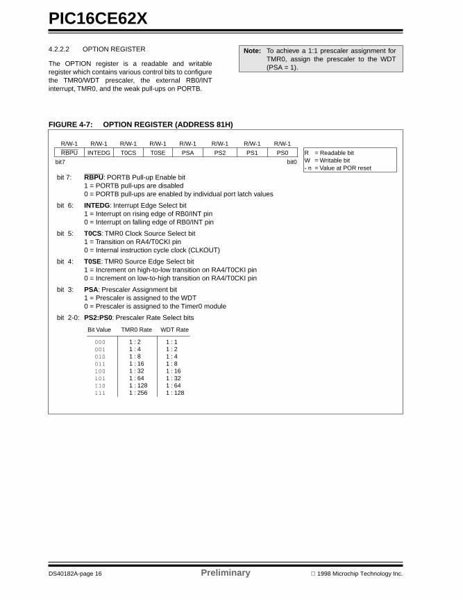
4.2.2.2 OPTION REGISTER
The OPTION register is a readable and writableregister which contains various control bits to configurethe TMR0/WDT prescaler, the external RB0/INTinterrupt, TMR0, and the weak pull-ups on PORTB.
DS40182A-page 16 Prelimin
Note: To achieve a 1:1 prescaler assignment forTMR0, assign the prescaler to the WDT(PSA = 1).
FIGURE 4-7: OPTION REGISTER (ADDRESS 81H)
R/W-1 R/W-1 R/W-1 R/W-1 R/W-1 R/W-1 R/W-1 R/W-1
RBPU INTEDG T0CS T0SE PSA PS2 PS1 PS0 R = Readable bitW = Writable bit- n = Value at POR reset
bit7 bit0
bit 7: RBPU: PORTB Pull-up Enable bit1 = PORTB pull-ups are disabled0 = PORTB pull-ups are enabled by individual port latch values
bit 6: INTEDG: Interrupt Edge Select bit1 = Interrupt on rising edge of RB0/INT pin0 = Interrupt on falling edge of RB0/INT pin
bit 5: T0CS: TMR0 Clock Source Select bit1 = Transition on RA4/T0CKI pin0 = Internal instruction cycle clock (CLKOUT)
bit 4: T0SE: TMR0 Source Edge Select bit1 = Increment on high-to-low transition on RA4/T0CKI pin0 = Increment on low-to-high transition on RA4/T0CKI pin
bit 3: PSA: Prescaler Assignment bit1 = Prescaler is assigned to the WDT0 = Prescaler is assigned to the Timer0 module
bit 2-0: PS2:PS0: Prescaler Rate Select bits
000001010011100101110111
1 : 21 : 41 : 81 : 161 : 321 : 641 : 1281 : 256
1 : 11 : 21 : 41 : 81 : 161 : 321 : 641 : 128
Bit Value TMR0 Rate WDT Rate
ary 1998 Microchip Technology Inc.

PIC16CE62X
62X.bk Page 17 Tuesday, March 10, 1998 3:40 PM
4.2.2.3 INTCON REGISTER
The INTCON register is a readable and writableregister which contains the various enable and flag bitsfor all interrupt sources except the comparator module.See Section 4.2.2.4 and Section 4.2.2.5 for adescription of the comparator enable and flag bits.
1998 Microchip Technology Inc. Prelimin
Note: Interrupt flag bits get set when an interruptcondition occurs regardless of the state ofits corresponding enable bit or the globalenable bit, GIE (INTCON<7>).
FIGURE 4-8: INTCON REGISTER (ADDRESS 0BH OR 8BH)
R/W-0 R/W-0 R/W-0 R/W-0 R/W-0 R/W-0 R/W-0 R/W-x
GIE PEIE T0IE INTE RBIE T0IF INTF RBIF R = Readable bitW = Writable bitU = Unimplemented bit,
read as ‘0’- n = Value at POR reset-x = Unknown at POR reset
bit7 bit0
bit 7: GIE: Global Interrupt Enable bit1 = Enables all un-masked interrupts0 = Disables all interrupts
bit 6: PEIE: Peripheral Interrupt Enable bit1 = Enables all un-masked peripheral interrupts0 = Disables all peripheral interrupts
bit 5: T0IE: TMR0 Overflow Interrupt Enable bit1 = Enables the TMR0 interrupt0 = Disables the TMR0 interrupt
bit 4: INTE: RB0/INT External Interrupt Enable bit1 = Enables the RB0/INT external interrupt0 = Disables the RB0/INT external interrupt
bit 3: RBIE: RB Port Change Interrupt Enable bit1 = Enables the RB port change interrupt0 = Disables the RB port change interrupt
bit 2: T0IF: TMR0 Overflow Interrupt Flag bit1 = TMR0 register has overflowed (must be cleared in software)0 = TMR0 register did not overflow
bit 1: INTF: RB0/INT External Interrupt Flag bit1 = The RB0/INT external interrupt occurred (must be cleared in software)0 = The RB0/INT external interrupt did not occur
bit 0: RBIF: RB Port Change Interrupt Flag bit1 = When at least one of the RB7:RB4 pins changed state (must be cleared in software)0 = None of the RB7:RB4 pins have changed state
ary DS40182A-page 17
PIC16CE62X
62X.bk Page 18 Tuesday, March 10, 1998 3:40 PM
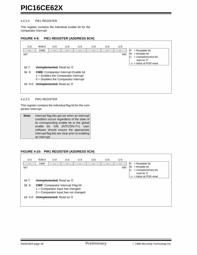
4.2.2.4 PIE1 REGISTER
This register contains the individual enable bit for thecomparator interrupt.
DS40182A-page 18 Prelimin
FIGURE 4-9: PIE1 REGISTER (ADDRESS 8CH)
U-0 R/W-0 U-0 U-0 U-0 U-0 U-0 U-0
— CMIE — — — — — — R = Readable bitW = Writable bitU = Unimplemented bit,
read as ‘0’- n = Value at POR reset
bit7 bit0
bit 7: Unimplemented: Read as '0'
bit 6: CMIE: Comparator Interrupt Enable bit1 = Enables the Comparator interrupt0 = Disables the Comparator interrupt
bit 5-0: Unimplemented: Read as '0'
4.2.2.5 PIR1 REGISTER
This register contains the individual flag bit for the com-parator interrupt.
Note: Interrupt flag bits get set when an interruptcondition occurs regardless of the state ofits corresponding enable bit or the globalenable bit, GIE (INTCON<7>). Usersoftware should ensure the appropriateinterrupt flag bits are clear prior to enablingan interrupt.
FIGURE 4-10: PIR1 REGISTER (ADDRESS 0CH)
U-0 R/W-0 U-0 U-0 U-0 U-0 U-0 U-0
— CMIF — — — — — — R = Readable bitW = Writable bitU = Unimplemented bit,
read as ‘0’- n = Value at POR reset
bit7 bit0
bit 7: Unimplemented: Read as '0'
bit 6: CMIF: Comparator Interrupt Flag bit1 = Comparator input has changed0 = Comparator input has not changed
bit 5-0: Unimplemented: Read as '0'
ary 1998 Microchip Technology Inc.

PIC16CE62X
62X.bk Page 19 Tuesday, March 10, 1998 3:40 PM
4.2.2.6 PCON REGISTER
The PCON register contains flag bits to differentiatebetween a Power-on Reset, an external MCLR reset,WDT reset or a Brown-out Reset.
Note: BOR is unknown on Power-on Reset. Itmust then be set by the user and checkedon subsequent resets to see if BOR iscleared, indicating a brown-out hasoccurred. The BOR status bit is a "don'tcare" and is not necessarily predictable ifthe brown-out circuit is disabled (byprogramming BODEN bit in theConfiguration word).
1998 Microchip Technology Inc. Prelimin
FIGURE 4-11: PCON REGISTER (ADDRESS 8Eh)
U-0 U-0 U-0 U-0 U-0 U-0 R/W-0 R/W-0
— — — — — — POR BOR R = Readable bitW = Writable bitU = Unimplemented bit,
read as ‘0’- n = Value at POR reset
bit7 bit0
bit 7-2: Unimplemented: Read as '0'
bit 1: POR: Power-on Reset Status bit1 = No Power-on Reset occurred0 = A Power-on Reset occurred (must be set in software after a Power-on Reset occurs)
bit 0: BOR: Brown-out Reset Status bit1 = No Brown-out Reset occurred0 = A Brown-out Reset occurred (must be set in software after a Brown-out Reset occurs)
ary DS40182A-page 19

PIC16CE62X
62X.bk Page 20 Tuesday, March 10, 1998 3:40 PM
4.3 PCL and PCLATH
The program counter (PC) is 13-bits wide. The low bytecomes from the PCL register, which is a readable andwritable register. The high byte (PC<12:8>) is not directlyreadable or writable and comes from PCLATH. On anyreset, the PC is cleared. Figure 4-12 shows the twosituations for the loading of the PC. The upper example inthe figure shows how the PC is loaded on a write to PCL(PCLATH<4:0> → PCH). The lower example in the figureshows how the PC is loaded during a CALL or GOTOinstruction (PCLATH<4:3> → PCH).
FIGURE 4-12: LOADING OF PC IN DIFFERENT SITUATIONS
4.3.1 COMPUTED GOTO
A computed GOTO is accomplished by adding anoffset to the program counter (ADDWF PCL). When doinga table read using a computed GOTO method, careshould be exercised if the table location crosses a PCLmemory boundary (each 256 byte block). Refer to theapplication note “Implementing a Table Read" (AN556).
PC
12 8 7 0
5PCLATH<4:0>
PCLATH
Instruction with
ALU result
GOTO, CALL
Opcode <10:0>
8
PC
12 11 10 0
11PCLATH<4:3>
PCH PCL
8 7
2
PCLATH
PCH PCL
PCL as Destination
DS40182A-page 20 Prelimin
4.3.2 STACK
The PIC16CE62X family has an 8 level deep x 13-bitwide hardware stack (Figure 4-2 and Figure 4-3). Thestack space is not part of either program or data spaceand the stack pointer is not readable or writable. ThePC is PUSHed onto the stack when a CALL instructionis executed or an interrupt causes a branch. The stackis POPed in the event of a RETURN, RETLW or a RETFIEinstruction execution. PCLATH is not affected by aPUSH or POP operation.
The stack operates as a circular buffer. This means thatafter the stack has been PUSHed eight times, the ninthpush overwrites the value that was stored from the firstpush. The tenth push overwrites the second push (andso on).
Note 1: There are no STATUS bits to indicatestack overflow or stack underflowconditions.
Note 2: There are no instruction mnemonicscalled PUSH or POP. These are actionsthat occur from the execution of theCALL, RETURN, RETLW and RETFIEinstructions, or the vectoring to aninterrupt address.
ary 1998 Microchip Technology Inc.

PIC16CE62X
62X.bk Page 21 Tuesday, March 10, 1998 3:40 PM
4.4 Indirect Addressing, INDF and FSR Registers
The INDF register is not a physical register. Addressingthe INDF register will cause indirect addressing.
Indirect addressing is possible by using the INDF reg-ister. Any instruction using the INDF register actuallyaccesses data pointed to by the file select register(FSR). Reading INDF itself indirectly will produce 00h.Writing to the INDF register indirectly results in ano-operation (although status bits may be affected). Aneffective 9-bit address is obtained by concatenating the8-bit FSR register and the IRP bit (STATUS<7>), asshown in Figure 4-13. However, IRP is not used in thePIC16CE62X.
1998 Microchip Technology Inc. Prelimin
A simple program to clear RAM location 20h-2Fh usingindirect addressing is shown in Example 4-1.
EXAMPLE 4-1: INDIRECT ADDRESSING
movlw 0x20 ;initialize pointer
movwf FSR ;to RAM
NEXT clrf INDF ;clear INDF register
incf FSR ;inc pointer
btfss FSR,4 ;all done?
goto NEXT ;no clear next
;yes continueCONTINUE:
FIGURE 4-13: DIRECT/INDIRECT ADDRESSING PIC16CE62X
For memory map detail see Figure 4-4 and Figure 4-5.
Note 1: The RP1 and IRP bits are reserved, always maintain these bits clear.
DataMemory
Indirect AddressingDirect Addressing
bank select location select
(1)RP1 RP0 6 0from opcode IRP(1) FSR register7 0
bank select location select
00 01 10 1100h
7Fh
00h
7Fh
Bank 0 Bank 1 Bank 2 Bank 3
not used
ary DS40182A-page 21

PIC16CE62X
62X.bk Page 22 Tuesday, March 10, 1998 3:40 PM
NOTES:
DS40182A-page 22 Prelimin
ary 1998 Microchip Technology Inc.


PIC16CE62X
62X.bk Page 25 Tuesday, March 10, 1998 3:40 PM
TABLE 5-1: PORTA FUNCTIONS
TABLE 5-2: SUMMARY OF REGISTERS ASSOCIATED WITH PORTA
Name Bit #Buffer Type
Function
RA0/AN0 bit0 ST Input/output or comparator inputRA1/AN1 bit1 ST Input/output or comparator inputRA2/AN2/VREF bit2 ST Input/output or comparator input or VREF outputRA3/AN3 bit3 ST Input/output or comparator input/outputRA4/T0CKI bit4 ST Input/output or external clock input for TMR0 or comparator output.
Output is open drain type.Legend: ST = Schmitt Trigger input
Address Name Bit 7 Bit 6 Bit 5 Bit 4 Bit 3 Bit 2 Bit 1 Bit 0Value on:
POR / BOR
Value on All OtherResets
05h PORTA — — — RA4 RA3 RA2 RA1 RA0 ---x 0000 ---u 0000
85h TRISA — — — TRISA4 TRISA3 TRISA2 TRISA1 TRISA0 ---1 1111 ---1 1111
1Fh CMCON C2OUT C1OUT — — CIS CM2 CM1 CM0 00-- 0000 00-- 0000
9Fh VRCON VREN VROE VRR — VR3 VR2 VR1 VR0 000- 0000 000- 0000
Legend: — = Unimplemented locations, read as ‘0’
Note: Note: Shaded bits are not used by PORTA.
1998 Microchip Technology Inc. Preliminary DS40182A-page 25

PIC16CE62X
62X.bk Page 27 Tuesday, March 10, 1998 3:40 PM
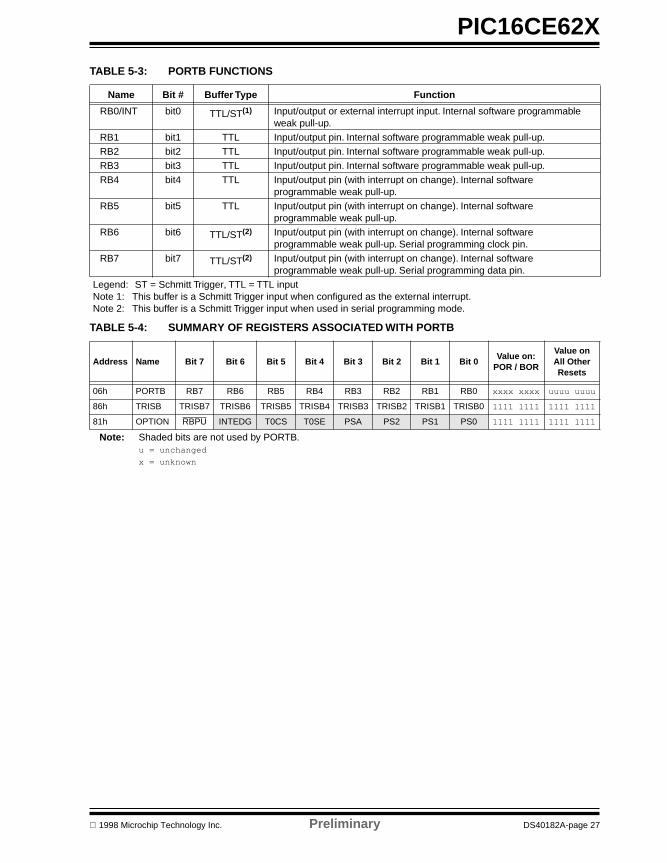
TABLE 5-3: PORTB FUNCTIONS
TABLE 5-4: SUMMARY OF REGISTERS ASSOCIATED WITH PORTB
Name Bit # Buffer Type Function
RB0/INT bit0 TTL/ST(1) Input/output or external interrupt input. Internal software programmable weak pull-up.
RB1 bit1 TTL Input/output pin. Internal software programmable weak pull-up.RB2 bit2 TTL Input/output pin. Internal software programmable weak pull-up.RB3 bit3 TTL Input/output pin. Internal software programmable weak pull-up.RB4 bit4 TTL Input/output pin (with interrupt on change). Internal software
programmable weak pull-up.RB5 bit5 TTL Input/output pin (with interrupt on change). Internal software
programmable weak pull-up.RB6 bit6 TTL/ST(2) Input/output pin (with interrupt on change). Internal software
programmable weak pull-up. Serial programming clock pin.RB7 bit7 TTL/ST(2) Input/output pin (with interrupt on change). Internal software
programmable weak pull-up. Serial programming data pin.Legend: ST = Schmitt Trigger, TTL = TTL inputNote 1: This buffer is a Schmitt Trigger input when configured as the external interrupt.Note 2: This buffer is a Schmitt Trigger input when used in serial programming mode.
Address Name Bit 7 Bit 6 Bit 5 Bit 4 Bit 3 Bit 2 Bit 1 Bit 0Value on:
POR / BOR
Value onAll Other Resets
06h PORTB RB7 RB6 RB5 RB4 RB3 RB2 RB1 RB0 xxxx xxxx uuuu uuuu
86h TRISB TRISB7 TRISB6 TRISB5 TRISB4 TRISB3 TRISB2 TRISB1 TRISB0 1111 1111 1111 1111
81h OPTION RBPU INTEDG T0CS T0SE PSA PS2 PS1 PS0 1111 1111 1111 1111
Note: Shaded bits are not used by PORTB.u = unchanged
x = unknown
1998 Microchip Technology Inc. Preliminary DS40182A-page 27


PIC16CE62X
62X.bk Page 29 Tuesday, March 10, 1998 3:40 PM
6.0 EEPROM PERIPHERAL OPERATION
The PIC16CE623/624/625 each have 128 bytes ofEEPROM data memory. The EEPROM data memorysupports a bi-directional 2-wire bus and data transmis-sion protocol. These two-wires are serial data (SDA)and serial clock (SCL), that are mapped to bit1 and bit2,respectively, of the EEINTF register (SFR 90h). Inaddition, the power to the EEPROM can be controlledusing bit0 (EEVDD) of the EEINTF register. For mostapplications, all that is required is calls to the followingfunctions:
; Byte_Write: Byte write routine; Inputs: EEPROM Address EEADDR; EEPROM Data EEDATA; Outputs: Return 01 in W if OK, else return 00 in W;; Read_Current: Read EEPROM at address currently held by EE device. ; Inputs: NONE; Outputs: EEPROM Data EEDATA; Return 01 in W if OK, else return 00 in W;; Read_Random: Read EEPROM byte at supplied address; Inputs: EEPROM Address EEADDR; Outputs: EEPROM Data EEDATA; Return 01 in W if OK,
else return 00 in W
1998 Microchip Technology Inc. Prelimin
The code for these functions is not yet determined, butwill be available on our web site (www.microchip.com)when it is completed. The code will be accessed byeither including the source code FLASH62X.INC or bylinking FLASH62X.ASM.
6.0.1 SERIAL DATA
SDA is a bi-directional pin used to transfer addressesand data into and data out of the memory.
For normal data transfer SDA is allowed to change onlyduring SCL low. Changes during SCL high arereserved for indicating the START and STOP condi-tions.
6.0.2 SERIAL CLOCK
This SCL input is used to synchronize the data transferfrom and to the memory.
6.0.3 EEINTF REGISTER
The EEINTF register (SFR 90h) controls the access tothe EEPROM. Figure 6.1 details the function of eachbit. User code must generate the clock and data sig-nals.
FIGURE 6-1: EEINFT REGISTER (ADDRESS 90h)
U-0 U-0 U-0 U-0 U-0 R/W-1 R/W-1 R/W-1
- - - - - EESCL EESDA EEVDD R = Readable bitW = Writable bitU = Unimplemented bit,
read as ‘0’- n = Value at POR reset
bit7 bit0
bit 7-3: Unimplemented: Read as '0'
bit 2: EESCL: Clock line to the EEPROM1 = Clock high0 = Clock low
bit 1: EESDA: Data line to EEPROM1 = Data line is high (pin is tri-stated, line is pulled high by a pull-up resistor)0 = Data line is low
bit 0: EEVDD: VDD control bit for EEPROM 1 = VDD is turned on EEPROM0 = VDD is turned off EEPROM (all pins are tri-stated and the EEPROM is powered down)
Note: EESDA, EESCL and EEVDD will read ‘0’ if EEVDD is turned off
ary DS40182A-page 29

PIC16CE62X
62X.bk Page 30 Tuesday, March 10, 1998 3:40 PM
6.1 BUS CHARACTERISTICS
In this section, the term “processor” refers to the portionof the PIC16CE62X that interfaces to the EEPROMthrough software manipulating the EEINTF register.The following bus protocol is to be used with theEEPROM data memory.
• Data transfer may be initiated only when the bus is not busy.
• During data transfer, the data line must remain stable whenever the clock line is HIGH. Changes in the data line while the clock line is HIGH will be interpreted by the EEPROM as a START or STOP condition.
Accordingly, the following bus conditions have beendefined (Figure 6-2).
6.1.1 BUS NOT BUSY (A)
Both data and clock lines remain HIGH.
6.1.2 START DATA TRANSFER (B)
A HIGH to LOW transition of the SDA line while theclock (SCL) is HIGH determines a START condition. Allcommands must be preceded by a START condition.
6.1.3 STOP DATA TRANSFER (C)
A LOW to HIGH transition of the SDA line while theclock (SCL) is HIGH determines a STOP condition. Alloperations must be ended with a STOP condition.
6.1.4 DATA VALID (D)
The state of the data line represents valid data when,after a START condition, the data line is stable for theduration of the HIGH period of the clock signal.
The data on the line must be changed during the LOWperiod of the clock signal. There is one bit of data perclock pulse.
Each data transfer is initiated with a START conditionand terminated with a STOP condition. The number ofthe data bytes transferred between the START andSTOP conditions is determined by the processor andis theoretically unlimited, although only the last sixteenwill be stored when doing a write operation. When anoverwrite does occur, it will replace data in a first-in,first-out fashion.
DS40182A-page 30 Prelimin
6.1.5 ACKNOWLEDGE
The EEPROM will generate an acknowledge after thereception of each byte. The processor must generatean extra clock pulse which is associated with thisacknowledge bit.
When the EEPROM acknowledges, it pulls down theSDA line during the acknowledge clock pulse in such away that the SDA line is stable LOW during the HIGHperiod of the acknowledge related clock pulse. Ofcourse, setup and hold times must be taken intoaccount. The processor must signal an end of data tothe EEPROM by not generating an acknowledge bit onthe last byte that has been clocked out of the EEPROM.In this case, the EEPROM must leave the data lineHIGH to enable the processor to generate the STOPcondition (Figure 6-3).
Note: Acknowledge bits are not generated if aninternal programming cycle is in progress.
ary 1998 Microchip Technology Inc.

PIC16CE62X
62X.bk Page 31 Tuesday, March 10, 1998 3:40 PM
FIGURE 6-2: DATA TRANSFER SEQUENCE ON THE SERIAL BUS
FIGURE 6-3: ACKNOWLEDGE TIMING
(A) (B) (C) (D) (A)(C)SCL
SDA
STARTCONDITION
ADDRESS ORACKNOWLEDGE
VALID
DATAALLOWED
TO CHANGE
STOPCONDITION
SCL 987654321 1 2 3
Transmitter must release the SDA line at this pointallowing the Receiver to pull the SDA line low toacknowledge the previous eight bits of data.
Receiver must release the SDA line at this pointso the Transmitter can continue sending data.
Data from transmitter Data from transmitterSDA
AcknowledgeBit
6.2 Device Addressing
After generating a START condition, the processortransmits a control byte consisting of a EEPROMaddress and a Read/Write bit that indicates what typeof operation is to be performed. The EEPROM addressconsists of a 4-bit device code (1010) followed by threedon't care bits.
The last bit of the control byte determines the operationto be performed. When set to a one a read operation isselected, and when set to a zero a write operation isselected. (Figure 6-4). The bus is monitored for its cor-responding EEPROM address all the time. It generatesan acknowledge bit if the EEPROM address was trueand it is not in a programming mode.
1998 Microchip Technology Inc. Prelimin
FIGURE 6-4: CONTROL BYTE FORMAT
1 0 1 0 X X XS ACKR/W
Device SelectBits
Don’t CareBits
EEPROM Address
Acknowledge BitStart Bit
Read/Write Bit
ary DS40182A-page 31
PIC16CE62X
62X.bk Page 32 Tuesday, March 10, 1998 3:40 PM
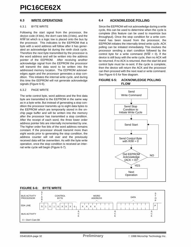
6.3 WRITE OPERATIONS
6.3.1 BYTE WRITE
Following the start signal from the processor, thedevice code (4 bits), the don't care bits (3 bits), and theR/W bit which is a logic low is placed onto the bus bythe processor. This indicates to the EEPROM that abyte with a word address will follow after it has gener-ated an acknowledge bit during the ninth clock cycle.Therefore the next byte transmitted by the processor isthe word address and will be written into the addresspointer of the EEPROM. After receiving anotheracknowledge signal from the EEPROM the processorwill transmit the data word to be written into theaddressed memory location. The EEPROM acknowl-edges again and the processor generates a stop con-dition. This initiates the internal write cycle, and duringthis time the EEPROM will not generate acknowledgesignals (Figure 6-6).
6.3.2 PAGE WRITE
The write control byte, word address and the first databyte are transmitted to the EEPROM in the same wayas in a byte write. But instead of generating a stop con-dition the processor transmits up to eight data bytes tothe EEPROM which are temporarily stored in the on-chip page buffer and will be written into the memoryafter the processor has transmitted a stop condition.After the receipt of each word, the three lower orderaddress pointer bits are internally incremented by one.The higher order five bits of the word address remainsconstant. If the processor should transmit more thaneight words prior to generating the stop condition, theaddress counter will roll over and the previouslyreceived data will be overwritten. As with the byte writeoperation, once the stop condition is received an inter-nal write cycle will begin (Figure 6-7).
FIGURE 6-6: BYTE WRITE
DS40182A-page 32 Prelimin
6.4 ACKNOWLEDGE POLLING
Since the EEPROM will not acknowledge during a writecycle, this can be used to determine when the cycle iscomplete (this feature can be used to maximize busthroughput). Once the stop condition for a write com-mand has been issued from the processor, theEEPROM initiates the internally timed write cycle. ACKpolling can be initiated immediately. This involves theprocessor sending a start condition followed by thecontrol byte for a write command (R/W = 0). If thedevice is still busy with the write cycle, then no ACK willbe returned. If no ACK is returned, then the start bit andcontrol byte must be re-sent. If the cycle is complete,then the device will return the ACK and the processorcan then proceed with the next read or write command.See Figure 6-5 for flow diagram.
FIGURE 6-5: ACKNOWLEDGE POLLING FLOW
SendWrite Command
Send StopCondition to
Initiate Write Cycle
Send Start
Send Control Bytewith R/W = 0
Did EEPROMAcknowledge(ACK = 0)?
NextOperation
NO
YES
S P
BUS ACTIVITYPROCESSOR
SDA LINE
BUS ACTIVITY
START
STOP
CONTROLBYTE
WORDADDRESS DATA
ACK
ACK
ACK
1 0 X1 0 XX X
X = Don’t Care Bit
X X X0
ary 1998 Microchip Technology Inc.

PIC16CE62X
62X.bk Page 33 Tuesday, March 10, 1998 3:40 PM
FIGURE 6-7: PAGE WRITE
S P
BUS ACTIVITY PROCESSOR
SDA LINE
BUS ACTIVITY
START
STOP
CONTROLBYTE
WORDADDRESS (n) DATA n DATAn + 7DATAn + 1
ACK
ACK
ACK
ACK
ACK
6.5 READ OPERATION
Read operations are initiated in the same way as writeoperations with the exception that the R/W bit of theEEPROM address is set to one. There are three basictypes of read operations: current address read, randomread, and sequential read.
6.6 Current Address Read
The EEPROM contains an address counter that main-tains the address of the last word accessed, internallyincremented by one. Therefore, if the previous access(either a read or write operation) was to address n, thenext current address read operation would access datafrom address n + 1. Upon receipt of the EEPROMaddress with R/W bit set to one, the EEPROM issuesan acknowledge and transmits the eight bit data word.The processor will not acknowledge the transfer butdoes generate a stop condition and the EEPROM dis-continues transmission (Figure 6-8).
6.7 Random Read
Random read operations allow the processor to accessany memory location in a random manner. To performthis type of read operation, first the word address mustbe set. This is done by sending the word address to theEEPROM as part of a write operation. After the wordaddress is sent, the processor generates a start condi-tion following the acknowledge. This terminates thewrite operation, but not before the internal addresspointer is set. Then the processor issues the controlbyte again but with the R/W bit set to a one. TheEEPROM will then issue an acknowledge and trans-mits the eight bit data word. The processor will notacknowledge the transfer but does generate a stopcondition and the EEPROM discontinues transmission(Figure 6-9).
1998 Microchip Technology Inc. Prelimin
6.8 Sequential Read
Sequential reads are initiated in the same way as a ran-dom read except that after the EEPROM transmits thefirst data byte, the processor issues an acknowledge asopposed to a stop condition in a random read. Thisdirects the EEPROM to transmit the next sequentiallyaddressed 8-bit word (Figure 6-10).
To provide sequential reads the EEPROM contains aninternal address pointer which is incremented by one atthe completion of each operation. This address pointerallows the entire memory contents to be serially readduring one operation.
6.9 Noise Protection
The EEPROM employs a VCC threshold detector circuitwhich disables the internal erase/write logic if the VCC
is below 1.5 volts at nominal conditions.
The SCL and SDA inputs have Schmitt trigger and filtercircuits which suppress noise spikes to assure properdevice operation even on a noisy bus.
ary DS40182A-page 33

PIC16CE62X
62X.bk Page 34 Tuesday, March 10, 1998 3:40 PM
FIGURE 6-8: CURRENT ADDRESS READ
FIGURE 6-9: RANDOM READ
FIGURE 6-10: SEQUENTIAL READ
S P
BUS ACTIVITY PROCESSOR
SDA LINE
BUS ACTIVITY
START
CONTROLBYTE DATA n
ACK
NO ACK
STOP
S PS
BUS ACTIVITY PROCESSOR
SDA LINE
BUS ACTIVITY
START
STOP
CONTROLBYTE
WORDADDRESS (n) DATA n
ACK
ACK
NO ACK
CONTROLBYTE
ACK
START
PSDA LINE
BUS ACTIVITY
STOP
CONTROLBYTE
DATA nACK
NO ACK
ACK
ACK
ACK
DATA n + 1 DATA n + 2 DATA n + X
BUS ACTIVITYPROCESSOR
DS40182A-page 34 Preliminary 1998 Microchip Technology Inc.

PIC16CE62X
62X.bk Page 35 Tuesday, March 10, 1998 3:40 PM
7.0 TIMER0 MODULEThe Timer0 module timer/counter has the followingfeatures:
• 8-bit timer/counter• Readable and writable• 8-bit software programmable prescaler• Internal or external clock select• Interrupt on overflow from FFh to 00h• Edge select for external clock
Figure 7-1 is a simplified block diagram of the Timer0module.
Timer mode is selected by clearing the T0CS bit(OPTION<5>). In timer mode, the TMR0 will incrementevery instruction cycle (without prescaler). If Timer0 iswritten, the increment is inhibited for the following twocycles (Figure 7-2 and Figure 7-3). The user can workaround this by writing an adjusted value to TMR0.
Counter mode is selected by setting the T0CS bit. Inthis mode Timer0 will increment either on every risingor falling edge of pin RA4/T0CKI. The incrementingedge is determined by the source edge (T0SE) control
1998 Microchip Technology Inc. Prelimin
bit (OPTION<4>). Clearing the T0SE bit selects therising edge. Restrictions on the external clock input arediscussed in detail in Section 7.2.
The prescaler is shared between the Timer0 moduleand the WatchdogTimer. The prescaler assignment iscontrolled in software by the control bit PSA(OPTION<3>). Clearing the PSA bit will assign theprescaler to Timer0. The prescaler is not readable orwritable. When the prescaler is assigned to the Timer0module, prescale value of 1:2, 1:4, ..., 1:256 areselectable. Section 7.3 details the operation of theprescaler.
7.1 TIMER0 Interrupt
Timer0 interrupt is generated when the TMR0 registertimer/counter overflows from FFh to 00h. This overflowsets the T0IF bit. The interrupt can be masked byclearing the T0IE bit (INTCON<5>). The T0IF bit(INTCON<2>) must be cleared in software by theTimer0 module interrupt service routine beforere-enabling this interrupt. The Timer0 interrupt cannotwake the processor from SLEEP since the timer is shutoff during SLEEP. See Figure 7-4 for Timer0 interrupttiming.
FIGURE 7-1: TIMER0 BLOCK DIAGRAM
FIGURE 7-2: TIMER0 (TMR0) TIMING: INTERNAL CLOCK/NO PRESCALER
Note 1: Bits T0SE, T0CS, PS2, PS1, PS0 and PSA are located in the OPTION register.2: The prescaler is shared with Watchdog Timer (Figure 7-6)
RA4/T0CKI
T0SE
0
1
1
0
pin
T0CS
FOSC/4
ProgrammablePrescaler
Sync withInternalclocks
TMR0
PSout
(2 cycle delay)
PSout
Data bus
8
Set Flag bit T0IFon OverflowPSAPS2:PS0
PC-1
Q1 Q2 Q3 Q4 Q1 Q2 Q3 Q4 Q1 Q2 Q3 Q4 Q1 Q2 Q3 Q4 Q1 Q2 Q3 Q4 Q1 Q2 Q3 Q4 Q1 Q2 Q3 Q4 Q1 Q2 Q3 Q4PC(ProgramCounter)
InstructionFetch
TMR0
PC PC+1 PC+2 PC+3 PC+4 PC+5 PC+6
T0 T0+1 T0+2 NT0 NT0 NT0 NT0+1 NT0+2 T0
MOVWF TMR0 MOVF TMR0,W MOVF TMR0,W MOVF TMR0,W MOVF TMR0,W MOVF TMR0,W
Write TMR0executed
Read TMR0reads NT0
Read TMR0reads NT0
Read TMR0reads NT0
Read TMR0reads NT0 + 1
Read TMR0reads NT0 + 2
InstructionExecuted
ary DS40182A-page 35

PIC16CE62X
62X.bk Page 36 Tuesday, March 10, 1998 3:40 PM
FIGURE 7-3: TIMER0 TIMING: INTERNAL CLOCK/PRESCALE 1:2
FIGURE 7-4: TIMER0 INTERRUPT TIMING
PC-1
Q1 Q2 Q3 Q4 Q1 Q2 Q3 Q4 Q1 Q2 Q3 Q4 Q1 Q2 Q3 Q4 Q1 Q2 Q3 Q4 Q1 Q2 Q3 Q4 Q1 Q2 Q3 Q4 Q1 Q2 Q3 Q4PC(ProgramCounter)
InstructionFetch
TMR0
PC PC+1 PC+2 PC+3 PC+4 PC+5 PC+6
T0 NT0+1
MOVWF TMR0 MOVF TMR0,W MOVF TMR0,W MOVF TMR0,W MOVF TMR0,W MOVF TMR0,W
Write TMR0executed
Read TMR0reads NT0
Read TMR0reads NT0
Read TMR0reads NT0
Read TMR0reads NT0
Read TMR0reads NT0 + 1
T0+1 NT0
InstructionExecute
Q2Q1 Q3 Q4Q2Q1 Q3 Q4 Q2Q1 Q3 Q4 Q2Q1 Q3 Q4 Q2Q1 Q3 Q4
1 1
OSC1
CLKOUT(3)
TMR0 timer
T0IF bit(INTCON<2>)
FEh
GIE bit(INTCON<7>)
INSTRUCTION FLOW
PC
Instructionfetched
PC PC +1 PC +1 0004h 0005h
Instructionexecuted
Inst (PC)
Inst (PC-1)
Inst (PC+1)
Inst (PC)
Inst (0004h) Inst (0005h)
Inst (0004h)Dummy cycle Dummy cycle
FFh 00h 01h 02h
Note 1: T0IF interrupt flag is sampled here (every Q1).2: Interrupt latency = 4TCY, where TCY = instruction cycle time.3: CLKOUT is available only in RC oscillator mode.
Interrupt Latency Time
DS40182A-page 36 Preliminary 1998 Microchip Technology Inc.

PIC16CE62X
62X.bk Page 37 Tuesday, March 10, 1998 3:40 PM
7.2 Using Timer0 with External Clock
When an external clock input is used for Timer0, it mustmeet certain requirements. The external clockrequirement is due to internal phase clock (TOSC)synchronization. Also, there is a delay in the actualincrementing of Timer0 after synchronization.
7.2.1 EXTERNAL CLOCK SYNCHRONIZATION
When no prescaler is used, the external clock input isthe same as the prescaler output. The synchronizationof T0CKI with the internal phase clocks isaccomplished by sampling the prescaler output on theQ2 and Q4 cycles of the internal phase clocks(Figure 7-5). Therefore, it is necessary for T0CKI to behigh for at least 2TOSC (and a small RC delay of 20 ns)and low for at least 2TOSC (and a small RC delay of20 ns). Refer to the electrical specification of thedesired device.
1998 Microchip Technology Inc. Prelimin
When a prescaler is used, the external clock input isdivided by the asynchronous ripple-counter typeprescaler so that the prescaler output is symmetrical.For the external clock to meet the samplingrequirement, the ripple-counter must be taken intoaccount. Therefore, it is necessary for T0CKI to have aperiod of at least 4TOSC (and a small RC delay of40 ns) divided by the prescaler value. The onlyrequirement on T0CKI high and low time is that they donot violate the minimum pulse width requirement of10 ns. Refer to parameters 40, 41 and 42 in theelectrical specification of the desired device.
7.2.2 TIMER0 INCREMENT DELAY
Since the prescaler output is synchronized with theinternal clocks, there is a small delay from the time theexternal clock edge occurs to the time the TMR0 isactually incremented. Figure 7-5 shows the delay fromthe external clock edge to the timer incrementing.
FIGURE 7-5: TIMER0 TIMING WITH EXTERNAL CLOCK
Q1 Q2 Q3 Q4 Q1 Q2 Q3 Q4 Q1 Q2 Q3 Q4 Q1 Q2 Q3 Q4
External Clock Input orPrescaler output (2)
External Clock/PrescalerOutput after sampling
Increment Timer0 (Q4)
Timer0 T0 T0 + 1 T0 + 2
Small pulsemisses sampling
Note 1: Delay from clock input change to Timer0 increment is 3Tosc to 7Tosc. (Duration of Q = Tosc).Therefore, the error in measuring the interval between two edges on Timer0 input = ±4Tosc max.
2: External clock if no prescaler selected, Prescaler output otherwise.3: The arrows indicate the points in time where sampling occurs.
(3)
(1)
ary DS40182A-page 37

PIC16CE62X
62X.bk Page 38 Tuesday, March 10, 1998 3:40 PM
7.3 Prescaler
An 8-bit counter is available as a prescaler for theTimer0 module, or as a postscaler for the WatchdogTimer, respectively (Figure 7-6). For simplicity, thiscounter is being referred to as “prescaler” throughoutthis data sheet. Note that there is only one prescaleravailable which is mutually exclusive between theTimer0 module and the Watchdog Timer. Thus, aprescaler assignment for the Timer0 module meansthat there is no prescaler for the Watchdog Timer, andvice-versa.
DS40182A-page 38 Prelimin
The PSA and PS2:PS0 bits (OPTION<3:0>) determinethe prescaler assignment and prescale ratio.
When assigned to the Timer0 module, all instructionswriting to the TMR0 register (e.g., CLRF 1, MOVWF 1,BSF 1,x....etc.) will clear the prescaler. Whenassigned to WDT, a CLRWDT instruction will clear theprescaler along with the Watchdog Timer. Theprescaler is not readable or writable.
FIGURE 7-6: BLOCK DIAGRAM OF THE TIMER0/WDT PRESCALER
T0CKI
T0SE
pin
MUX
CLKOUT (=Fosc/4)
SYNC2
CyclesTMR0 reg
8-bit Prescaler
8-to-1MUX
MUX
M U X
WatchdogTimer
PSA
0 1
0
1
WDTTime-out
PS0 - PS2
8
Note: T0SE, T0CS, PSA, PS0-PS2 are bits in the OPTION register.
PSA
WDT Enable bit
MUX
0
1 0
1
Data Bus
Set flag bit T0IFon Overflow
8
PSAT0CS
ary 1998 Microchip Technology Inc.


PIC16CE62X
62X.bk Page 40 Tuesday, March 10, 1998 3:40 PM
NOTES:
DS40182A-page 40 Preliminary 1998 Microchip Technology Inc.

PIC16CE62X
62X.bk Page 41 Tuesday, March 10, 1998 3:40 PM
8.0 COMPARATOR MODULEThe comparator module contains two analogcomparators. The inputs to the comparators aremultiplexed with the RA0 through RA3 pins. Theon-chip Voltage Reference (Section 9.0) can also be aninput to the comparators.
1998 Microchip Technology Inc. Prelimin
The CMCON register, shown in Figure 8-1, controls thecomparator input and output multiplexers. A blockdiagram of the comparator is shown in Figure 8-2.
FIGURE 8-1: CMCON REGISTER (ADDRESS 1Fh)
R-0 R-0 U-0 U-0 R/W-0 R/W-0 R/W-0 R/W-0C2OUT C1OUT CIS CM2 CM1 CM0 R = Readable bit
W = Writable bitU = Unimplemented bit,
read as ‘0’- n =Value at POR reset
bit7 bit0
bit 7: C2OUT: Comparator 2 output1 = C2 VIN+ > C2 VIN–0 = C2 VIN+ < C2 VIN–
bit 6: C1OUT: Comparator 1 output1 = C1 VIN+ > C1 VIN–0 = C1 VIN+ < C1 VIN–
bit 5-4: Unimplemented: Read as '0'
bit 3: CIS: Comparator Input SwitchWhen CM<2:0>: = 001:1 = C1 VIN– connects to RA30 = C1 VIN– connects to RA0When CM<2:0> = 010:1 = C1 VIN– connects to RA3 C2 VIN– connects to RA20 = C1 VIN– connects to RA0 C2 VIN– connects to RA1
bit 2-0: CM<2:0>: Comparator modeFigure 8-2.
ary DS40182A-page 41

PIC16CE62X
62X.bk Page 42 Tuesday, March 10, 1998 3:40 PM
8.1 Comparator Configuration
There are eight modes of operation for thecomparators. The CMCON register is used to select themode. Figure 8-2 shows the eight possible modes. TheTRISA register controls the data direction of the com-parator pins for each mode. If the comparator mode is
DS40182A-page 42 Prelimin
changed, the comparator output level may not be validfor the specified mode change delay shown inTable 13-2.
Note: Comparator interrupts should be disabledduring a comparator mode change other-wise a false interrupt may occur.
FIGURE 8-2: COMPARATOR I/O OPERATING MODES
-
+C1
VIN-
VIN+Off
(Read as '0')RA0/AN0
RA3/AN3
A
A
CM<2:0> = 000
-
+C2
VIN-
VIN+Off
(Read as '0')RA1/AN1
RA2/AN2
A
A
-
+C1
VIN-
VIN+Off
(Read as '0')RA0/AN0
RA3/AN3
D
D
CM<2:0> = 111
-
+C2
VIN-
VIN+Off
(Read as '0')RA1/AN1
RA2/AN2
D
D
-
+C1
VIN-
VIN+ C1OUTRA0/AN0
RA3/AN3
A
A
-
+C2
VIN-
VIN+ C2OUTRA1/AN1
RA2/AN2
A
A
CM<2:0> = 100
-
+C1
VIN-
VIN+ C1OUT
RA0/AN0
RA3/AN3
A
A
-
+C2
VIN-
VIN+ C2OUT
RA1/AN1
RA2/AN2
A
A
From VREF Module
-
+C1
VIN-
VIN+ C1OUTRA0/AN0
RA3/AN3
A
D
-
+C2
VIN-
VIN+ C2OUTRA1/AN1
RA2/AN2
A
A
CM<2:0> = 011 RA4 Open Drain
-
+C1
VIN-
VIN+ C1OUTRA0/AN0
RA3/AN3
A
D
-
+C2
VIN-
VIN+ C2OUTRA1/AN1
RA2/AN2
A
A
CM<2:0> = 110
-
+C1
VIN-
VIN+Off
(Read as '0')RA0/AN0
RA3/AN3
D
D
CM<2:0> = 101
-
+C2
VIN-
VIN+ C2OUTRA1/AN1
RA2/AN2
A
A
-
+C1
VIN-
VIN+ C1OUT
RA0/AN0
RA3/AN3
A
A
-
+C2
VIN-
VIN+ C2OUTRA1/AN1
RA2/AN2
A
A
CM<2:0> = 001
CIS=0
CIS=1
Comparators Reset
Two Independent Comparators
Two Common Reference Comparators
One Independent Comparator Three Inputs Multiplexed to
Two Common Rference Comparators with Outputs
Four Inputs Multiplexed to
Comparators Off
Two Comparators
Two Comparators
CM<2:0> = 010
CIS=0
CIS=1
CIS=0
CIS=1
A = Analog Input, Port Reads Zeros AlwaysD = Digital InputCIS = CMCON<3>, Comparator Input Switch
ary 1998 Microchip Technology Inc.

PIC16CE62X
62X.bk Page 43 Tuesday, March 10, 1998 3:40 PM
The code example in Example 8-1 depicts the stepsrequired to configure the comparator module. RA3 andRA4 are configured as digital output. RA0 and RA1 areconfigured as the V- inputs and RA2 as the V+ input toboth comparators.
EXAMPLE 8-1: INITIALIZING COMPARATOR MODULE
8.2 Comparator Operation
A single comparator is shown in Figure 8-3 along withthe relationship between the analog input levels andthe digital output. When the analog input at VIN+ is lessthan the analog input VIN–, the output of thecomparator is a digital low level. When the analog inputat VIN+ is greater than the analog input VIN–, the outputof the comparator is a digital high level. The shadedareas of the output of the comparator in Figure 8-3represent the uncertainty due to input offsets andresponse time.
FLAG_REG EQU 0X20CLRF FLAG_REG ;Init flag registerCLRF PORTA ;Init PORTAMOVF CMCON,W ;Move comparator contents to WANDLW 0xC0 ;Mask comparator bitsIORWF FLAG_REG,F ;Store bits in flag registerMOVLW 0x03 ;Init comparator modeMOVWF CMCON ;CM<2:0> = 011 BSF STATUS,RP0 ;Select Bank1MOVLW 0x07 ;Initialize data directionMOVWF TRISA ;Set RA<2:0> as inputs
;RA<4:3> as outputs;TRISA<7:5> always read ‘0’
BCF STATUS,RP0 ;Select Bank 0CALL DELAY 10 ;10µs delayMOVF CMCON,F ;Read CMCON to end change conditionBCF PIR1,CMIF ;Clear pending interruptsBSF STATUS,RP0 ;Select Bank 1BSF PIE1,CMIE ;Enable comparator interruptsBCF STATUS,RP0 ;Select Bank 0BSF INTCON,PEIE ;Enable peripheral interruptsBSF INTCON,GIE ;Global interrupt enable
1998 Microchip Technology Inc. Prelimin
8.3 Comparator Reference
An external or internal reference signal may be useddepending on the comparator operating mode. Theanalog signal that is present at VIN– is compared to thesignal at VIN+, and the digital output of the comparatoris adjusted accordingly (Figure 8-3).
FIGURE 8-3: SINGLE COMPARATOR
8.3.1 EXTERNAL REFERENCE SIGNAL
When external voltage references are used, thecomparator module can be configured to have the com-parators operate from the same or different referencesources. However, threshold detector applications mayrequire the same reference. The reference signal mustbe between VSS and VDD, and can be applied to eitherpin of the comparator(s).
8.3.2 INTERNAL REFERENCE SIGNAL
The comparator module also allows the selection of aninternally generated voltage reference for thecomparators. Section 13, Instruction Sets, contains adetailed description of the Voltage Reference Modulethat provides this signal. The internal reference signalis used when the comparators are in modeCM<2:0>=010 (Figure 8-2). In this mode, the internalvoltage reference is applied to the VIN+ pin of both com-parators.
–+VIN+
VIN–Output
VIN–
VIN+
Output
ary DS40182A-page 43


PIC16CE62X
62X.bk Page 45 Tuesday, March 10, 1998 3:40 PM
8.6 Comparator Interrupts
The comparator interrupt flag is set whenever there isa change in the output value of either comparator.Software will need to maintain information about thestatus of the output bits, as read from CMCON<7:6>, todetermine the actual change that has occurred. TheCMIF bit, PIR1<6>, is the comparator interrupt flag.The CMIF bit must be reset by clearing ‘0’. Since it isalso possible to write a '1' to this register, a simulatedinterrupt may be initiated.
The CMIE bit (PIE1<6>) and the PEIE bit(INTCON<6>) must be set to enable the interrupt. Inaddition, the GIE bit must also be set. If any of thesebits are clear, the interrupt is not enabled, though theCMIF bit will still be set if an interrupt condition occurs.
The user, in the interrupt service routine, can clear theinterrupt in the following manner:
a) Any read or write of CMCON. This will end themismatch condition.
b) Clear flag bit CMIF.
A mismatch condition will continue to set flag bit CMIF.Reading CMCON will end the mismatch condition, andallow flag bit CMIF to be cleared.
8.7 Comparator Operation During SLEEP
When a comparator is active and the device is placedin SLEEP mode, the comparator remains active andthe interrupt is functional if enabled. This interrupt will
Note: If a change in the CMCON register(C1OUT or C2OUT) should occur when aread operation is being executed (start ofthe Q2 cycle), then the CMIF (PIR1<6>)interrupt flag may not get set.
1998 Microchip Technology Inc. Prelimin
wake up the device from SLEEP mode when enabled.While the comparator is powered-up, higher sleepcurrents than shown in the power down currentspecification will occur. Each comparator that isoperational will consume additional current as shown inthe comparator specifications. To minimize powerconsumption while in SLEEP mode, turn off thecomparators, CM<2:0> = 111, before entering sleep. Ifthe device wakes-up from sleep, the contents of theCMCON register are not affected.
8.8 Effects of a RESET
A device reset forces the CMCON register to its resetstate. This forces the comparator module to be in thecomparator reset mode, CM2:CM0 = 000. Thisensures that all potential inputs are analog inputs.Device current is minimized when analog inputs arepresent at reset time. The comparators will bepowered-down during the reset interval.
8.9 Analog Input Connection Considerations
A simplified circuit for an analog input is shown inFigure 8-5. Since the analog pins are connected to adigital output, they have reverse biased diodes to VDD
and VSS. The analog input therefore, must be betweenVSS and VDD. If the input voltage deviates from thisrange by more than 0.6V in either direction, one of thediodes is forward biased and a latch-up may occur. Amaximum source impedance of 10 kΩ isrecommended for the analog sources. Any externalcomponent connected to an analog input pin, such asa capacitor or a Zener diode, should have very littleleakage current.
FIGURE 8-5: ANALOG INPUT MODEL
VA
RS
AIN
CPIN5 pF
VDD
VT = 0.6V
VT = 0.6V
RIC < 10K
ILEAKAGE±500 nA
VSS
Legend CPIN = Input CapacitanceVT = Threshold VoltageILEAKAGE = Leakage Current At The Pin Due To Various JunctionsRIC = Interconnect ResistanceRS = Source ImpedanceVA = Analog Voltage
ary DS40182A-page 45

PIC16CE62X
62X.bk Page 46 Tuesday, March 10, 1998 3:40 PM
TABLE 8-1: REGISTERS ASSOCIATED WITH COMPARATOR MODULE
Note: x = Unknown- = Unimplemented, read as "0"
Address Name Bit 7 Bit 6 Bit 5 Bit 4 Bit 3 Bit 2 Bit 1 Bit 0Value on
POR / BOR
Value onAll OtherResets
1Fh CMCON C2OUT C1OUT — — CIS CM2 CM1 CM0 00-- 0000 00-- 0000
9Fh VRCON VREN VROE VRR — VR3 VR2 VR1 VR0 000- 0000 000- 0000
0Bh INTCON GIE PEIE T0IE INTE RBIE T0IF INTF RBIF 0000 000x 0000 000x
0Ch PIR1 — CMIF — — — — — — -0-- ---- -0-- ----
8Ch PIE1 — CMIE — — — — — — -0-- ---- -0-- ----
85h TRISA — — — TRISA4 TRISA3 TRISA2 TRISA1 TRISA0 ---1 1111 ---1 1111
DS40182A-page 46 Preliminary 1998 Microchip Technology Inc.


PIC16CE62X
62X.bk Page 48 Tuesday, March 10, 1998 3:40 PM
EXAMPLE 9-1: VOLTAGE REFERENCE CONFIGURATION
9.2 Voltage Reference Accuracy/Error
The full range of VSS to VDD cannot be realized due tothe construction of the module. The transistors on thetop and bottom of the resistor ladder network(Figure 9-2) keep VREF from approaching VSS or VDD.The Voltage Reference is VDD derived and therefore,the VREF output changes with fluctuations in VDD. Theabsolute accuracy of the Voltage Reference can befound in Table 13-3.
9.3 Operation During Sleep
When the device wakes up from sleep through aninterrupt or a Watchdog Timer time-out, the contents ofthe VRCON register are not affected. To minimizecurrent consumption in SLEEP mode, the VoltageReference should be disabled.
MOVLW 0x02 ; 4 Inputs Muxed
MOVWF CMCON ; to 2 comps.
BSF STATUS,RP0 ; go to Bank 1
MOVLW 0x07 ; RA3-RA0 are
MOVWF TRISA ; outputs
MOVLW 0xA6 ; enable VREF
MOVWF VRCON ; low range
; set VR<3:0>=6
BCF STATUS,RP0 ; go to Bank 0
CALL DELAY10 ; 10µs delay
DS40182A-page 48 Prelimin
9.4 Effects of a Reset
A device reset disables the Voltage Reference by clear-ing bit VREN (VRCON<7>). This reset also disconnectsthe reference from the RA2 pin by clearing bit VROE
(VRCON<6>) and selects the high voltage range byclearing bit VRR (VRCON<5>). The VREF value selectbits, VRCON<3:0>, are also cleared.
9.5 Connection Considerations
The Voltage Reference Module operates independentlyof the comparator module. The output of the referencegenerator may be connected to the RA2 pin if theTRISA<2> bit is set and the VROE bit, VRCON<6>, isset. Enabling the Voltage Reference output onto theRA2 pin with an input signal present will increase cur-rent consumption. Connecting RA2 as a digital outputwith VREF enabled will also increase current consump-tion.
The RA2 pin can be used as a simple D/A output withlimited drive capability. Due to the limited drivecapability, a buffer must be used in conjunction with theVoltage Reference output for external connections toVREF. Figure 9-3 shows an example bufferingtechnique.
FIGURE 9-3: VOLTAGE REFERENCE OUTPUT BUFFER EXAMPLE
TABLE 9-1: REGISTERS ASSOCIATED WITH VOLTAGE REFERENCE
Note: - = Unimplemented, read as "0"
Address Name Bit 7 Bit 6 Bit 5 Bit 4 Bit 3 Bit 2 Bit 1 Bit 0Value On
POR / BOR
Value OnAll OtherResets
9Fh VRCON VREN VROE VRR — VR3 VR2 VR1 VR0 000- 0000 000- 0000
1Fh CMCON C2OUT C1OUT — — CIS CM2 CM1 CM0 00-- 0000 00-- 0000
85h TRISA — — — TRISA4 TRISA3 TRISA2 TRISA1 TRISA0 ---1 1111 ---1 1111
VREF Output+– ••
VREF Module
Voltage Reference
Output Impedance
R(1) RA2
Note 1: R is dependent upon the Voltage Reference Configuration VRCON<3:0> and VRCON<5>.
ary 1998 Microchip Technology Inc.

PIC16CE62X
62X.bk Page 49 Tuesday, March 10, 1998 3:40 PM
10.0 SPECIAL FEATURES OF THE CPU
What sets a microcontroller apart from otherprocessors are special circuits to deal with the needs ofreal time applications. The PIC16CE62X family has ahost of such features intended to maximize systemreliability, minimize cost through elimination of externalcomponents, provide power saving operating modesand offer code protection.
These are:
1. OSC selection2. Reset
Power-on Reset (POR)Power-up Timer (PWRT)Oscillator Start-Up Timer (OST)Brown-out Reset (BOR)
3. Interrupts4. Watchdog Timer (WDT)5. SLEEP6. Code protection7. ID Locations8. In-circuit serial programming
1998 Microchip Technology Inc. Prelimin
The PIC16CE62X has a Watchdog Timer which iscontrolled by configuration bits. It runs off its own RCoscillator for added reliability. There are two timers thatoffer necessary delays on power-up. One is theOscillator Start-up Timer (OST), intended to keep thechip in reset until the crystal oscillator is stable. Theother is the Power-up Ttimer (PWRT), which provides afixed delay of 72 ms (nominal) on power-up only,designed to keep the part in reset while the powersupply stabilizes. There is also circuitry to reset thedevice if a brown-out occurs which provides at least a72 ms reset. With these three functions on-chip, mostapplications need no external reset circuitry.
The SLEEP mode is designed to offer a very lowcurrent power-down mode. The user can wake-up fromSLEEP through external reset, Watchdog Timerwake-up or through an interrupt. Several oscillatoroptions are also made available to allow the part to fitthe application. The RC oscillator option saves systemcost while the LP crystal option saves power. A set ofconfiguration bits are used to select various options.
ary DS40182A-page 49

PIC16CE62X
62X.bk Page 50 Tuesday, March 10, 1998 3:40 PM
10.1 Configuration Bits
The configuration bits can be programmed (read as '0')or left unprogrammed (read as '1') to select variousdevice configurations. These bits are mapped inprogram memory location 2007h.
The user will note that address 2007h is beyond the user program memory space. In fact, it belongsto the special test/configuration memory space(2000h – 3FFFh), which can be accessed only duringprogramming.
FIGURE 10-1: CONFIGURATION WORD
CP1 CP0(2) CP1 CP0(2) CP1 CP0(2) — BODE(1) CP1 CP0(2) PWRTE(1) WDTE F0SC1 F0SC0 CONFIG AddressREGISTER: 2007hbit13 bit0
bit 13-8 CP1:CP0 Pairs: Code protection bits(2)
5-4: Code protection for 2K program memory11 = Program memory code protection off10 = 0400h-07FFh code protected01 = 0200h-07FFh code protected00 = 0000h-07FFh code protectedCode protection for 1K program memory11 = Program memory code protection off10 =Program memory code protection on01 = 0200h-03FFh code protected00 = 0000h-03FFh code protectedCode protection for 0.5K program memory11 = Program memory code protection off10 = Program memory code protection of01 = Program memory code protection of00 = 0000h-01FFh code protected
bit 7: Unimplemented: Read as '1'
bit 6: BODEN: Brown-out Reset Enable bit (1)
1 = BOR enabled0 = BOR disabled
bit 3: PWRTE: Power-up Timer Enable bit (1)
1 = PWRT disabled0 = PWRT enabled
bit 2: WDTE: Watchdog Timer Enable bit1 = WDT enabled0 = WDT disabled
bit 1-0: FOSC1:FOSC0: Oscillator Selection bits11 = RC oscillator10 = HS oscillator01 = XT oscillator00 = LP oscillator
Note 1: Enabling Brown-out Reset automatically enables Power-up Timer (PWRT) regardless of the value of bit PWRTE. Ensure the Power-up Timer is enabled anytime Brown-out Reset is enabled.
2: All of the CP1:CP0 pairs have to be given the same value to enable the code protection scheme listed.
DS40182A-page 50 Preliminary 1998 Microchip Technology Inc.


PIC16CE62X
62X.bk Page 53 Tuesday, March 10, 1998 3:40 PM
10.3 Reset
The PIC16CE62X differentiates between various kindsof reset:
a) Power-on reset (POR) b) MCLR reset during normal operationc) MCLR reset during SLEEP d) WDT reset (normal operation)e) WDT wake-up (SLEEP)f) Brown-out Reset (BOR)
Some registers are not affected in any reset condition;their status is unknown on POR and unchanged in anyother reset. Most other registers are reset to a “reset
state” on Power-on reset, on MCLR or WDT reset andon MCLR reset during SLEEP. They are not affected bya WDT wake-up, since this is viewed as the resumptionof normal operation. TO and PD bits are set or cleareddifferently in different reset situations as indicated inTable 10-4. These bits are used in software to deter-mine the nature of the reset. See Table 10-6 for a fulldescription of reset states of all registers.
A simplified block diagram of the on-chip reset circuit isshown in Figure 10-7.
The MCLR reset path has a noise filter to detect andignore small pulses. See Table 13-6 for pulse widthspecification.
FIGURE 10-7: SIMPLIFIED BLOCK DIAGRAM OF ON-CHIP RESET CIRCUIT
S
R Q
ExternalReset
MCLR/
VDD
OSC1/
WDTModule
VDD risedetect
OST/PWRT
On-chip(1) RC OSC
WDTTime-out
Power-on Reset
OST
PWRT
Chip_Reset
10-bit Ripple-counter
Reset
Enable OST
Enable PWRT
SLEEP
See Table 10-3 for time-out situations.
Note 1: This is a separate oscillator from the RC oscillator of the CLKIN pin.
Brown-outReset BODEN
CLKINPin
VPP Pin
10-bit Ripple-counter
1998 Microchip Technology Inc. Preliminary DS40182A-page 53

PIC16CE62X
62X.bk Page 54 Tuesday, March 10, 1998 3:40 PM
10.4 Power-on Reset (POR), Power-up Timer (PWRT), Oscillator Start-up Timer (OST) and Brown-out Reset (BOR)
10.4.1 POWER-ON RESET (POR)
The on-chip POR circuit holds the chip in reset untilVDD has reached a high enough level for proper opera-tion. To take advantage of the POR, just tie the MCLRpin directly (or through a resistor) to VDD. This willeliminate external RC components usually needed tocreate Power-on Reset. A maximum rise time for VDD
is required. See Electrical Specifications for details.
The POR circuit does not produce internal reset whenVDD declines.
When the device starts normal operation (exits thereset condition), device operating parameters (voltage,frequency, temperature, etc.) must be met to ensureoperation. If these conditions are not met, the devicemust be held in reset until the operating conditions aremet.
For additional information, refer to Application NoteAN607 “Power-up Trouble Shooting”.
10.4.2 POWER-UP TIMER (PWRT)
The Power-up Timer provides a fixed 72 ms (nominal)time-out on power-up only, from POR or Brown-outReset. The Power-up Timer operates on an internal RCoscillator. The chip is kept in reset as long as PWRT isactive. The PWRT delay allows the VDD to rise to anacceptable level. A configuration bit, PWRTE can
DS40182A-page 54 Prelimin
disable (if set) or enable (if cleared or programmed) thePower-up Timer. The Power-up Timer should always beenabled when Brown-out Reset is enabled.
The Power-Up Time delay will vary from chip to chipand due to VDD, temperature and process variation.See DC parameters for details.
10.4.3 OSCILLATOR START-UP TIMER (OST)
The Oscillator Start-Up Timer (OST) provides a 1024oscillator cycle (from OSC1 input) delay after thePWRT delay is over. This ensures that the crystaloscillator or resonator has started and stabilized.
The OST time-out is invoked only for XT, LP and HSmodes and only on power-on reset or wake-up fromSLEEP.
10.4.4 BROWN-OUT RESET (BOR)
The PIC16CE62X members have on-chip Brown-outReset circuitry. A configuration bit, BODEN, can dis-able (if clear/programmed) or enable (if set) theBrown-out Reset circuitry. If VDD falls below 4.0V (referto BVDD parameter D005) for greater than parameter(TBOR) in Table 13-6, the brown-out situation will resetthe chip. A reset is not guaranteed to occur if VDD fallsbelow 4.0V for less than parameter (TBOR). The chipwill remain in Brown-out Reset until VDD rises aboveBVDD. The Power-up Timer will now be invoked and willkeep the chip in reset an additional 72 ms. If VDD dropsbelow BVDD while the Power-up Timer is running, thechip will go back into a Brown-out Reset and thePower-up Timer will be initialized. Once VDD risesabove BVDD, the Power-Up Timer will execute a 72 msreset. The Power-up Timer should always be enabledwhen Brown-out Reset is enabled. Figure 10-8 showstypical Brown-out situations.
FIGURE 10-8: BROWN-OUT SITUATIONS
72 ms
BVDD VDD
InternalReset
BVDD VDD
InternalReset 72 ms<72 ms
72 ms
BVDD VDD
InternalReset
ary 1998 Microchip Technology Inc.

PIC16CE62X
62X.bk Page 55 Tuesday, March 10, 1998 3:40 PM
10.4.5 TIME-OUT SEQUENCE
On power-up the time-out sequence is as follows: FirstPWRT time-out is invoked after POR has expired. ThenOST is activated. The total time-out will vary based onoscillator configuration and PWRTE bit status. Forexample, in RC mode with PWRTE bit erased (PWRTdisabled), there will be no time-out at all. Figure 10-9,Figure 10-10 and Figure 10-11 depict time-outsequences.
Since the time-outs occur from the POR pulse, if MCLRis kept low long enough, the time-outs will expire. Thenbringing MCLR high will begin execution immediately(see Figure 10-10). This is useful for testing purposesor to synchronize more than one PICmicro device oper-ating in parallel.
Table 10-5 shows the reset conditions for some specialregisters, while Table 10-6 shows the reset conditionsfor all the registers.
10.4.6 POWER CONTROL (PCON)/STATUS REGISTER
The power control/status register, PCON (address8Eh) has two bits.
Bit0 is BO (Brown-out). BO is unknown onpower-on-reset. It must then be set by the user andchecked on subsequent resets to see if BO = 0indicating that a brown-out has occurred. The BOstatus bit is a don’t care and is not necessarilypredictable if the brown-out circuit is disabled (bysetting BODEN bit = 0 in the Configuration word).
Bit1 is POR (Power-on-reset). It is a ‘0’ onpower-on-reset and unaffected otherwise. The usermust write a ‘1’ to this bit following a power-on-reset.On a subsequent reset if POR is ‘0’, it will indicate thata power-on-reset must have occurred (VDD may havegone too low).
TABLE 10-3: TIME-OUT IN VARIOUS SITUATIONS
TABLE 10-4: STATUS/PCON BITS AND THEIR SIGNIFICANCE
Oscillator ConfigurationPower-up
Brown-out ResetWake-up
from SLEEPPWRTE = 0 PWRTE = 1
XT, HS, LP 72 ms + 1024 TOSC 1024 TOSC 72 ms + 1024 TOSC 1024 TOSC
RC 72 ms — 72 ms —
POR BOR TO PD
0 X 1 1 Power-on-reset
0 X 0 X Illegal, TO is set on POR
0 X X 0 Illegal, PD is set on POR
1 0 X X Brown-out Reset
1 1 0 1 WDT Reset
1 1 0 0 WDT Wake-up
1 1 u u MCLR reset during normal operation
1 1 1 0 MCLR reset during SLEEP
1998 Microchip Technology Inc. Preliminary DS40182A-page 55


PIC16CE62X
62X.bk Page 57 Tuesday, March 10, 1998 3:40 PM
FIGURE 10-9: TIME-OUT SEQUENCE ON POWER-UP (MCLR NOT TIED TO VDD): CASE 1
FIGURE 10-10: TIME-OUT SEQUENCE ON POWER-UP (MCLR NOT TIED TO VDD): CASE 2
FIGURE 10-11: TIME-OUT SEQUENCE ON POWER-UP (MCLR TIED TO VDD)
TPWRT
TOST
VDD
MCLR
INTERNAL POR
PWRT TIME-OUT
OST TIME-OUT
INTERNAL RESET
VDD
MCLR
INTERNAL POR
PWRT TIME-OUT
OST TIME-OUT
INTERNAL RESET
TPWRT
TOST
TPWRT
TOST
VDD
MCLR
INTERNAL POR
PWRT TIME-OUT
OST TIME-OUT
INTERNAL RESET
1998 Microchip Technology Inc. Preliminary DS40182A-page 57

PIC16CE62X
62X.bk Page 58 Tuesday, March 10, 1998 3:40 PM
FIGURE 10-12: EXTERNAL POWER-ON RESET CIRCUIT (FOR SLOW VDD POWER-UP)
Note 1: External power-on reset circuit is required only if VDD power-up slope is too slow. The diode D helps discharge the capaci-tor quickly when VDD powers down.
2: < 40 kΩ is recommended to make sure that voltage drop across R does not vio-late the device’s electrical specification.
3: R1 = 100Ω to 1 kΩ will limit any current flowing into MCLR from external capaci-tor C in the event of MCLR/VPP pin break-down due to Electrostatic Discharge (ESD) or Electrical Overstress (EOS).
C
R1
RD
VDD
MCLR
PIC16CE62X
VDD
DS40182A-page 58 Prelimin
FIGURE 10-13: EXTERNAL BROWN-OUT PROTECTION CIRCUIT 1
FIGURE 10-14: EXTERNAL BROWN-OUT PROTECTION CIRCUIT 2
Note 1: This circuit will activate reset when VDD goes below (Vz + 0.7V) where Vz = Zener voltage.
2: Internal Brown-out Reset circuitry should be disabled when using this cir-cuit.
VDD
33k
10k
40k
VDD
MCLR
PIC16CE62X
Note 1: This brown-out circuit is less expensive, albeit less accurate. Transistor Q1 turns off when VDD is below a certain level such that:
2: Internal brown-out detection should be disabled when using this circuit.
3: Resistors should be adjusted for the characteristics of the transistor.
VDD xR1
R1 + R2= 0.7 V
VDD
R2 40k
VDD
MCLR
PIC16CE62X
R1
Q1
ary 1998 Microchip Technology Inc.

PIC16CE62X
62X.bk Page 59 Tuesday, March 10, 1998 3:40 PM
10.5 Interrupts
The PIC16CE62X has 4 sources of interrupt:
• External interrupt RB0/INT• TMR0 overflow interrupt• PortB change interrupts (pins RB7:RB4)• Comparator interrupt
The interrupt control register (INTCON) recordsindividual interrupt requests in flag bits. It also hasindividual and global interrupt enable bits.
A global interrupt enable bit, GIE (INTCON<7>)enables (if set) all un-masked interrupts or disables (ifcleared) all interrupts. Individual interrupts can bedisabled through their corresponding enable bits inINTCON register. GIE is cleared on reset.
The “return from interrupt” instruction, RETFIE, exitsinterrupt routine as well as sets the GIE bit, whichre-enable RB0/INT interrupts.
The INT pin interrupt, the RB port change interrupt andthe TMR0 overflow interrupt flags are contained in theINTCON register.
The peripheral interrupt flag is contained in the specialregister PIR1. The corresponding interrupt enable bit iscontained in special registers PIE1.
When an interrupt is responded to, the GIE is clearedto disable any further interrupt, the return address ispushed into the stack and the PC is loaded with 0004h.Once in the interrupt service routine the source(s) of
the interrupt can be determined by polling the interruptflag bits. The interrupt flag bit(s) must be cleared in soft-ware before re-enabling interrupts to avoid RB0/INTrecursive interrupts.
For external interrupt events, such as the INT pin orPORTB change interrupt, the interrupt latency will bethree or four instruction cycles. The exact latencydepends when the interrupt event occurs(Figure 10-16). The latency is the same for one or twocycle instructions. Once in the interrupt service routinethe source(s) of the interrupt can be determined bypolling the interrupt flag bits. The interrupt flag bit(s)must be cleared in software before re-enabling inter-rupts to avoid multiple interrupt requests. Individualinterrupt flag bits are set regardless of the status oftheir corresponding mask bit or the GIE bit.
Note 1: Individual interrupt flag bits are setregardless of the status of theircorresponding mask bit or the GIE bit.
2: When an instruction that clears the GIEbit is executed, any interrupts that werepending for execution in the next cycleare ignored. The CPU will execute aNOP in the cycle immediately followingthe instruction which clears the GIE bit.The interrupts which were ignored arestill pending to be serviced when the GIEbit is set again.
FIGURE 10-15: INTERRUPT LOGIC
RBIFRBIE
T0IFT0IE
INTFINTE
GIE
PEIE
Wake-up(If in SLEEP mode)
Interrupt to CPU
CMIECMIF
1998 Microchip Technology Inc. Preliminary DS40182A-page 59

PIC16CE62X
62X.bk Page 60 Tuesday, March 10, 1998 3:40 PM
10.5.1 RB0/INT INTERRUPT
External interrupt on RB0/INT pin is edge triggered:either rising if INTEDG bit (OPTION<6>) is set, or fall-ing, if INTEDG bit is clear. When a valid edge appearson the RB0/INT pin, the INTF bit (INTCON<1>) is set.This interrupt can be disabled by clearing the INTEcontrol bit (INTCON<4>). The INTF bit must be clearedin software in the interrupt service routine beforere-enabling this interrupt. The RB0/INT interrupt canwake-up the processor from SLEEP, if the INTE bit wasset prior to going into SLEEP. The status of the GIE bitdecides whether or not the processor branches to theinterrupt vector following wake-up. See Section 10.8 fordetails on SLEEP and Figure 10-19 for timing ofwake-up from SLEEP through RB0/INT interrupt.
10.5.2 TMR0 INTERRUPT
An overflow (FFh → 00h) in the TMR0 register willset the T0IF (INTCON<2>) bit. The interrupt canbe enabled/disabled by setting/clearing T0IE(INTCON<5>) bit. For operation of the Timer0 module,see Section 7.0.
10.5.3 PORTB INTERRUPT
An input change on PORTB <7:4> sets the RBIF(INTCON<0>) bit. The interrupt can be enabled/dis-abled by setting/clearing the RBIE (INTCON<4>) bit.For operation of PORTB (Section 5.2).
10.5.4 COMPARATOR INTERRUPT
See Section 8.6 for complete description of comparatorinterrupts.
Note: If a change on the I/O pin should occurwhen the read operation is being executed(start of the Q2 cycle), then the RBIF inter-rupt flag may not get set.
FIGURE 10-16: INT PIN INTERRUPT TIMING
Q2Q1 Q3 Q4 Q2Q1 Q3 Q4 Q2Q1 Q3 Q4 Q2Q1 Q3 Q4 Q2Q1 Q3 Q4
OSC1
CLKOUT
INT pin
INTF flag(INTCON<1>)
GIE bit(INTCON<7>)
INSTRUCTION FLOW
PC
Instructionfetched
Instructionexecuted
Interrupt Latency
PC PC+1 PC+1 0004h 0005h
Inst (0004h) Inst (0005h)
Dummy Cycle
Inst (PC) Inst (PC+1)
Inst (PC-1) Inst (0004h)Dummy CycleInst (PC)
—
1
4
5
1
Note 1: INTF flag is sampled here (every Q1).2: Interrupt latency = 3-4 Tcy where Tcy = instruction cycle time.
Latency is the same whether Inst (PC) is a single cycle or a 2-cycle instruction.3: CLKOUT is available only in RC oscillator mode.4: For minimum width of INT pulse, refer to AC specs.5: INTF is enabled to be set anytime during the Q4-Q1 cycles.
2
3
DS40182A-page 60 Preliminary 1998 Microchip Technology Inc.
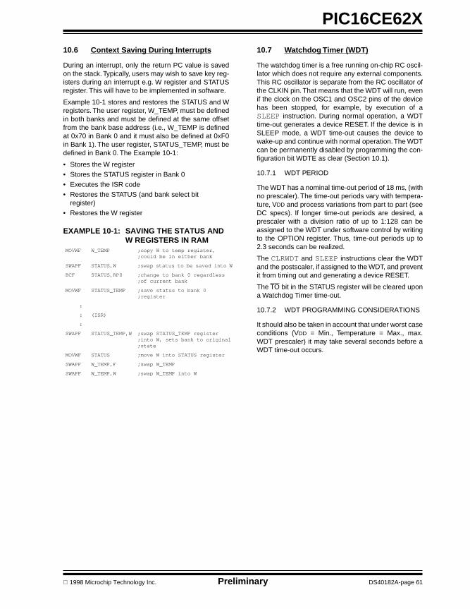
PIC16CE62X
62X.bk Page 61 Tuesday, March 10, 1998 3:40 PM
10.6 Context Saving During Interrupts
During an interrupt, only the return PC value is savedon the stack. Typically, users may wish to save key reg-isters during an interrupt e.g. W register and STATUSregister. This will have to be implemented in software.
Example 10-1 stores and restores the STATUS and Wregisters. The user register, W_TEMP, must be definedin both banks and must be defined at the same offsetfrom the bank base address (i.e., W_TEMP is definedat 0x70 in Bank 0 and it must also be defined at 0xF0in Bank 1). The user register, STATUS_TEMP, must bedefined in Bank 0. The Example 10-1:
• Stores the W register• Stores the STATUS register in Bank 0• Executes the ISR code• Restores the STATUS (and bank select bit
register)• Restores the W register
EXAMPLE 10-1: SAVING THE STATUS AND W REGISTERS IN RAM
MOVWF W_TEMP ;copy W to temp register, ;could be in either bank
SWAPF STATUS,W ;swap status to be saved into W
BCF STATUS,RP0 ;change to bank 0 regardless;of current bank
MOVWF STATUS_TEMP ;save status to bank 0 ;register
:
: (ISR)
:
SWAPF STATUS_TEMP,W ;swap STATUS_TEMP register;into W, sets bank to original;state
MOVWF STATUS ;move W into STATUS register
SWAPF W_TEMP,F ;swap W_TEMP
SWAPF W_TEMP,W ;swap W_TEMP into W
1998 Microchip Technology Inc. Prelimin
10.7 Watchdog Timer (WDT)
The watchdog timer is a free running on-chip RC oscil-lator which does not require any external components.This RC oscillator is separate from the RC oscillator ofthe CLKIN pin. That means that the WDT will run, evenif the clock on the OSC1 and OSC2 pins of the devicehas been stopped, for example, by execution of aSLEEP instruction. During normal operation, a WDTtime-out generates a device RESET. If the device is inSLEEP mode, a WDT time-out causes the device towake-up and continue with normal operation. The WDTcan be permanently disabled by programming the con-figuration bit WDTE as clear (Section 10.1).
10.7.1 WDT PERIOD
The WDT has a nominal time-out period of 18 ms, (withno prescaler). The time-out periods vary with tempera-ture, VDD and process variations from part to part (seeDC specs). If longer time-out periods are desired, aprescaler with a division ratio of up to 1:128 can beassigned to the WDT under software control by writingto the OPTION register. Thus, time-out periods up to2.3 seconds can be realized.
The CLRWDT and SLEEP instructions clear the WDTand the postscaler, if assigned to the WDT, and preventit from timing out and generating a device RESET.
The TO bit in the STATUS register will be cleared upona Watchdog Timer time-out.
10.7.2 WDT PROGRAMMING CONSIDERATIONS
It should also be taken in account that under worst caseconditions (VDD = Min., Temperature = Max., max.WDT prescaler) it may take several seconds before aWDT time-out occurs.
ary DS40182A-page 61

PIC16CE62X
62X.bk Page 62 Tuesday, March 10, 1998 3:40 PM
FIGURE 10-17: WATCHDOG TIMER BLOCK DIAGRAM
FIGURE 10-18: SUMMARY OF WATCHDOG TIMER REGISTERS
Address Name Bit 7 Bit 6 Bit 5 Bit 4 Bit 3 Bit 2 Bit 1 Bit 0
2007h Config. bits --- BODEN CP1 CP0 PWRTE WDTE FOSC1 FOSC0
81h OPTION RBPU INTEDG T0CS T0SE PSA PS2 PS1 PS0
Legend: Shaded cells are not used by the Watchdog Timer.
Note: _ = Unimplemented location, read as “0”+ = Reserved for future use
From TMR0 Clock Source(Figure 7-6)
To TMR0 (Figure 7-6)
PostscalerWatchdog
Timer
MUX
PSA
8 - to -1 MUX
PSA
WDT Time-out
10
0
1
WDT Enable Bit
PS<2:0>
•
•
Note: T0SE, T0CS, PSA, PS0-PS2 are bits in the OPTION register.
8
MUX
DS40182A-page 62 Preliminary 1998 Microchip Technology Inc.

PIC16CE62X
62X.bk Page 63 Tuesday, March 10, 1998 3:40 PM
10.8 Power-Down Mode (SLEEP)
The Power-down mode is entered by executing aSLEEP instruction.
If enabled, the Watchdog Timer will be cleared butkeeps running, the PD bit in the STATUS register iscleared, the TO bit is set, and the oscillator driver isturned off. The I/O ports maintain the status they had,before SLEEP was executed (driving high, low, orhi-impedance).
For lowest current consumption in this mode, all I/Opins should be either at VDD, or VSS, with no externalcircuitry drawing current from the I/O pin and the com-parators and VREF should be disabled. I/O pins that arehi-impedance inputs should be pulled high or low exter-nally to avoid switching currents caused by floatinginputs. The T0CKI input should also be at VDD or VSS
for lowest current consumption. The contribution fromon chip pull-ups on PORTB should be considered.
The MCLR pin must be at a logic high level (VIHMC).
10.8.1 WAKE-UP FROM SLEEP
The device can wake-up from SLEEP through one ofthe following events:
1. External reset input on MCLR pin2. Watchdog Timer Wake-up (if WDT was enabled)3. Interrupt from RB0/INT pin, RB Port change, or
the Peripheral Interrupt (Comparator).
The first event will cause a device reset. The two latterevents are considered a continuation of program exe-cution. The TO and PD bits in the STATUS register canbe used to determine the cause of device reset. PDbit, which is set on power-up is cleared when SLEEP isinvoked. TO bit is cleared if WDT Wake-up occurred.
When the SLEEP instruction is being executed, thenext instruction (PC + 1) is pre-fetched. For the deviceto wake-up through an interrupt event, the correspond-ing interrupt enable bit must be set (enabled). Wake-upis regardless of the state of the GIE bit. If the GIE bit isclear (disabled), the device continues execution at theinstruction after the SLEEP instruction. If the GIE bit isset (enabled), the device executes the instruction afterthe SLEEP instruction and then branches to the inter-rupt address (0004h). In cases where the execution ofthe instruction following SLEEP is not desirable, theuser should have an NOP after the SLEEP instruction.
The WDT is cleared when the device wakes-up fromsleep, regardless of the source of wake-up.
Note: It should be noted that a RESET generatedby a WDT time-out does not drive MCLRpin low.
Note: If the global interrupts are disabled (GIE iscleared), but any interrupt source has bothits interrupt enable bit and the correspond-ing interrupt flag bits set, the device willimmediately wakeup from sleep. The sleepinstruction is completely executed.
FIGURE 10-19: WAKE-UP FROM SLEEP THROUGH INTERRUPT
Q1 Q2 Q3 Q4 Q1 Q2 Q3 Q4 Q1 Q1 Q2 Q3 Q4 Q1 Q2 Q3 Q4 Q1 Q2 Q3 Q4 Q1 Q2 Q3 Q4
OSC1
CLKOUT(4)
INT pin
INTF flag(INTCON<1>)
GIE bit(INTCON<7>)
INSTRUCTION FLOW
PC
Instructionfetched
Instructionexecuted
PC PC+1 PC+2
Inst(PC) = SLEEP
Inst(PC - 1)
Inst(PC + 1)
SLEEP
Processor in
SLEEP
Interrupt Latency(Note 2)
Inst(PC + 2)
Inst(PC + 1)
Inst(0004h) Inst(0005h)
Inst(0004h)Dummy cycle
PC + 2 0004h 0005h
Dummy cycle
TOST(2)
PC+2
Note 1: XT, HS or LP oscillator mode assumed.2: TOST = 1024TOSC (drawing not to scale) This delay will not be there for RC osc mode.3: GIE = '1' assumed. In this case after wake- up, the processor jumps to the interrupt routine. If GIE = '0', execution will continue in-line.4: CLKOUT is not available in these osc modes, but shown here for timing reference.
1998 Microchip Technology Inc. Preliminary DS40182A-page 63

PIC16CE62X
62X.bk Page 64 Tuesday, March 10, 1998 3:40 PM
10.9 Code Protection
If the code protection bit(s) have not beenprogrammed, the on-chip program memory can beread out for verification purposes.
10.10 ID Locations
Four memory locations (2000h-2003h) are designatedas ID locations where the user can store checksum orother code-identification numbers. These locations arenot accessible during normal execution but arereadable and writable during program/verify. Only theleast significant 4 bits of the ID locations are used.
Note: Microchip does not recommend codeprotecting windowed devices.
DS40182A-page 64 Prelimin
10.11 In-Circuit Serial Programming
The PIC16CE62X microcontrollers can be seriallyprogrammed while in the end application circuit. This issimply done with two lines for clock and data, and threeother lines for power, ground, and the programmingvoltage. This allows customers to manufacture boardswith unprogrammed devices, and then program themicrocontroller just before shipping the product. Thisalso allows the most recent firmware or a customfirmware to be programmed.
The device is placed into a program/verify mode byholding the RB6 and RB7 pins low while raising theMCLR (VPP) pin from VIL to VIHH (see programmingspecification). RB6 becomes the programming clockand RB7 becomes the programming data. Both RB6and RB7 are Schmitt Trigger inputs in this mode.
After reset, to place the device into programming/verifymode, the program counter (PC) is at location 00h. A6-bit command is then supplied to the device.Depending on the command, 14-bits of program dataare then supplied to or from the device, depending if thecommand was a load or a read. For complete details ofserial programming, please refer to thePIC16C6X/7X/9XX Programming Specifications (Liter-ature #DS30228).
A typical in-circuit serial programming connection isshown in Figure 10-20.
FIGURE 10-20: TYPICAL IN-CIRCUIT SERIAL PROGRAMMING CONNECTION
ExternalConnectorSignals
To NormalConnections
To NormalConnections
PIC16CE62X
VDD
VSS
MCLR/VPP
RB6
RB7
+5V
0V
VPP
CLK
Data I/O
VDD
ary 1998 Microchip Technology Inc.

PIC16CE62X
62X.bk Page 65 Tuesday, March 10, 1998 3:40 PM
11.0 INSTRUCTION SET SUMMARYEach PIC16CE62X instruction is a 14-bit word dividedinto an OPCODE which specifies the instruction typeand one or more operands which further specify theoperation of the instruction. The PIC16CE62X instruc-tion set summary in Table 11-2 lists byte-oriented,bit-oriented, and literal and control operations.Table 11-1 shows the opcode field descriptions.
For byte-oriented instructions, 'f' represents a fileregister designator and 'd' represents a destinationdesignator. The file register designator specifies whichfile register is to be used by the instruction.
The destination designator specifies where the result ofthe operation is to be placed. If 'd' is zero, the result isplaced in the W register. If 'd' is one, the result is placedin the file register specified in the instruction.
For bit-oriented instructions, 'b' represents a bit fielddesignator which selects the number of the bit affectedby the operation, while 'f' represents the number of thefile in which the bit is located.
For literal and control operations, 'k' represents aneight or eleven bit constant or literal value.
TABLE 11-1: OPCODE FIELD DESCRIPTIONS
Field Description
f Register file address (0x00 to 0x7F)
W Working register (accumulator)
b Bit address within an 8-bit file register
k Literal field, constant data or label
x Don't care location (= 0 or 1) The assembler will generate code with x = 0. It is the recommended form of use for compatibility with all Microchip software tools.
d Destination select; d = 0: store result in W,d = 1: store result in file register f. Default is d = 1
label Label name
TOS Top of Stack
PC Program CounterPCLATH Program Counter High Latch
GIE Global Interrupt Enable bit
WDT Watchdog Timer/Counter
TO Time-out bit
PD Power-down bit
dest Destination either the W register or the specified register file location
[ ] Options
( ) Contents
→ Assigned to
< > Register bit field
∈ In the set of
italics User defined term (font is courier)
1998 Microchip Technology Inc. Prelimin
The instruction set is highly orthogonal and is groupedinto three basic categories:
• Byte-oriented operations• Bit-oriented operations• Literal and control operations
All instructions are executed within one singleinstruction cycle, unless a conditional test is true or theprogram counter is changed as a result of aninstruction. In this case, the execution takes twoinstruction cycles with the second cycle executed as aNOP. One instruction cycle consists of four oscillatorperiods. Thus, for an oscillator frequency of 4 MHz, thenormal instruction execution time is 1 µs. If aconditional test is true or the program counter ischanged as a result of an instruction, the instructionexecution time is 2 µs.
Table 11-1 lists the instructions recognized by theMPASM assembler.
Figure 11-1 shows the three general formats that theinstructions can have.
All examples use the following format to represent ahexadecimal number:
0xhh
where h signifies a hexadecimal digit.
FIGURE 11-1: GENERAL FORMAT FOR INSTRUCTIONS
Note: To maintain upward compatibility withfuture PICmicro™ products, do not use theOPTION and TRIS instructions.
Byte-oriented file register operations13 8 7 6 0
d = 0 for destination W
OPCODE d f (FILE #)
d = 1 for destination ff = 7-bit file register address
Bit-oriented file register operations13 10 9 7 6 0
OPCODE b (BIT #) f (FILE #)
b = 3-bit bit addressf = 7-bit file register address
Literal and control operations
13 8 7 0
OPCODE k (literal)
k = 8-bit immediate value
13 11 10 0
OPCODE k (literal)
k = 11-bit immediate value
General
CALL and GOTO instructions only
ary DS40182A-page 65


PIC16CE62X
62X.bk Page 67 Tuesday, March 10, 1998 3:40 PM
11.1 Instruction Descriptions
ADDLW Add Literal and W
Syntax: [ label ] ADDLW k
Operands: 0 ≤ k ≤ 255
Operation: (W) + k → (W)
Status Affected: C, DC, Z
Encoding: 11 111x kkkk kkkk
Description: The contents of the W register are added to the eight bit literal 'k' and the result is placed in the W register.
Words: 1
Cycles: 1
Example ADDLW 0x15
Before InstructionW = 0x10
After InstructionW = 0x25
ADDWF Add W and f
Syntax: [ label ] ADDWF f,d
Operands: 0 ≤ f ≤ 127d ∈ [0,1]
Operation: (W) + (f) → (dest)
Status Affected: C, DC, Z
Encoding: 00 0111 dfff ffff
Description: Add the contents of the W register with register 'f'. If 'd' is 0 the result is stored in the W register. If 'd' is 1 the result is stored back in register 'f'.
Words: 1
Cycles: 1
Example ADDWF FSR, 0
Before InstructionW = 0x17FSR = 0xC2
After InstructionW = 0xD9FSR = 0xC2
1998 Microchip Technology Inc. Prelimin
ANDLW AND Literal with W
Syntax: [ label ] ANDLW k
Operands: 0 ≤ k ≤ 255
Operation: (W) .AND. (k) → (W)
Status Affected: Z
Encoding: 11 1001 kkkk kkkk
Description: The contents of W register are AND’ed with the eight bit literal 'k'. The result is placed in the W register.
Words: 1
Cycles: 1
Example ANDLW 0x5F
Before InstructionW = 0xA3
After InstructionW = 0x03
ANDWF AND W with f
Syntax: [ label ] ANDWF f,d
Operands: 0 ≤ f ≤ 127d ∈ [0,1]
Operation: (W) .AND. (f) → (dest)
Status Affected: Z
Encoding: 00 0101 dfff ffff
Description: AND the W register with register 'f'. If 'd' is 0 the result is stored in the W register. If 'd' is 1 the result is stored back in register 'f'.
Words: 1
Cycles: 1
Example ANDWF FSR, 1
Before Instruction W = 0x17FSR = 0xC2
After InstructionW = 0x17FSR = 0x02
ary DS40182A-page 67

PIC16CE62X
62X.bk Page 68 Tuesday, March 10, 1998 3:40 PM
BCF Bit Clear f
Syntax: [ label ] BCF f,b
Operands: 0 ≤ f ≤ 1270 ≤ b ≤ 7
Operation: 0 → (f<b>)
Status Affected: None
Encoding: 01 00bb bfff ffff
Description: Bit 'b' in register 'f' is cleared.
Words: 1
Cycles: 1
Example BCF FLAG_REG, 7
Before InstructionFLAG_REG = 0xC7
After InstructionFLAG_REG = 0x47
BSF Bit Set f
Syntax: [ label ] BSF f,b
Operands: 0 ≤ f ≤ 1270 ≤ b ≤ 7
Operation: 1 → (f<b>)
Status Affected: None
Encoding: 01 01bb bfff ffff
Description: Bit 'b' in register 'f' is set.
Words: 1
Cycles: 1
Example BSF FLAG_REG, 7
Before InstructionFLAG_REG = 0x0A
After InstructionFLAG_REG = 0x8A
DS40182A-page 68 Prelimin
BTFSC Bit Test, Skip if Clear
Syntax: [ label ] BTFSC f,b
Operands: 0 ≤ f ≤ 1270 ≤ b ≤ 7
Operation: skip if (f<b>) = 0
Status Affected: None
Encoding: 01 10bb bfff ffff
Description: If bit 'b' in register 'f' is '0' then the next instruction is skipped.If bit 'b' is '0' then the next instruction fetched during the current instruction execution is discarded, and a NOP is executed instead, making this a two-cycle instruction.
Words: 1
Cycles: 1(2)
Example HEREFALSETRUE
BTFSCGOTO•••
FLAG,1PROCESS_CODE
Before InstructionPC = address HERE
After Instructionif FLAG<1> = 0,PC = address TRUEif FLAG<1>=1,PC = address FALSE
ary 1998 Microchip Technology Inc.

PIC16CE62X
62X.bk Page 69 Tuesday, March 10, 1998 3:40 PM
BTFSS Bit Test f, Skip if Set
Syntax: [ label ] BTFSS f,b
Operands: 0 ≤ f ≤ 1270 ≤ b < 7
Operation: skip if (f<b>) = 1
Status Affected: None
Encoding: 01 11bb bfff ffff
Description: If bit 'b' in register 'f' is '1' then the next instruction is skipped.If bit 'b' is '1', then the next instruction fetched during the current instruction execution, is discarded and a NOP is executed instead, making this a two-cycle instruction.
Words: 1
Cycles: 1(2)
Example HEREFALSETRUE
BTFSSGOTO•••
FLAG,1PROCESS_CODE
Before InstructionPC = address HERE
After Instructionif FLAG<1> = 0,PC = address FALSEif FLAG<1> = 1,PC = address TRUE
CALL Call Subroutine
Syntax: [ label ] CALL k
Operands: 0 ≤ k ≤ 2047
Operation: (PC)+ 1→ TOS,k → PC<10:0>,(PCLATH<4:3>) → PC<12:11>
Status Affected: None
Encoding: 10 0kkk kkkk kkkk
Description: Call Subroutine. First, return address (PC+1) is pushed onto the stack. The eleven bit immediate address is loaded into PC bits <10:0>. The upper bits of the PC are loaded from PCLATH. CALL is a two-cycle instruction.
Words: 1
Cycles: 2
Example HERE CALL THERE
Before InstructionPC = Address HERE
After InstructionPC = Address THERETOS = Address HERE+1
1998 Microchip Technology Inc. Prelimin
CLRF Clear f
Syntax: [ label ] CLRF f
Operands: 0 ≤ f ≤ 127
Operation: 00h → (f)1 → Z
Status Affected: Z
Encoding: 00 0001 1fff ffff
Description: The contents of register 'f' are cleared and the Z bit is set.
Words: 1
Cycles: 1
Example CLRF FLAG_REG
Before InstructionFLAG_REG = 0x5A
After InstructionFLAG_REG = 0x00Z = 1
CLRW Clear W
Syntax: [ label ] CLRW
Operands: None
Operation: 00h → (W)1 → Z
Status Affected: Z
Encoding: 00 0001 0xxx xxxx
Description: W register is cleared. Zero bit (Z) is set.
Words: 1
Cycles: 1
Example CLRW
Before InstructionW = 0x5A
After InstructionW = 0x00Z = 1
ary DS40182A-page 69

PIC16CE62X
62X.bk Page 70 Tuesday, March 10, 1998 3:40 PM
CLRWDT Clear Watchdog Timer
Syntax: [ label ] CLRWDT
Operands: None
Operation: 00h → WDT0 → WDT prescaler,1 → TO1 → PD
Status Affected: TO, PD
Encoding: 00 0000 0110 0100
Description: CLRWDT instruction resets the Watchdog Timer. It also resets the prescaler of the WDT. Status bits TO and PD are set.
Words: 1
Cycles: 1
Example CLRWDT
Before InstructionWDT counter = ?
After InstructionWDT counter = 0x00WDT prescaler= 0TO = 1PD = 1
COMF Complement f
Syntax: [ label ] COMF f,d
Operands: 0 ≤ f ≤ 127d ∈ [0,1]
Operation: (f) → (dest)
Status Affected: Z
Encoding: 00 1001 dfff ffff
Description: The contents of register 'f' are complemented. If 'd' is 0 the result is stored in W. If 'd' is 1 the result is stored back in register 'f'.
Words: 1
Cycles: 1
Example COMF REG1,0
Before InstructionREG1 = 0x13
After InstructionREG1 = 0x13W = 0xEC
DS40182A-page 70 Prelimin
DECF Decrement f
Syntax: [ label ] DECF f,d
Operands: 0 ≤ f ≤ 127d ∈ [0,1]
Operation: (f) - 1 → (dest)
Status Affected: Z
Encoding: 00 0011 dfff ffff
Description: Decrement register 'f'. If 'd' is 0 the result is stored in the W register. If 'd' is 1 the result is stored back in register 'f'.
Words: 1
Cycles: 1
Example DECF CNT, 1
Before InstructionCNT = 0x01Z = 0
After InstructionCNT = 0x00Z = 1
DECFSZ Decrement f, Skip if 0
Syntax: [ label ] DECFSZ f,d
Operands: 0 ≤ f ≤ 127d ∈ [0,1]
Operation: (f) - 1 → (dest); skip if result = 0
Status Affected: None
Encoding: 00 1011 dfff ffff
Description: The contents of register 'f' are decremented. If 'd' is 0 the result is placed in the W register. If 'd' is 1 the result is placed back in register 'f'. If the result is 0, the next instruction, which is already fetched, is discarded. A NOP is executed instead making it a two-cycle instruction.
Words: 1
Cycles: 1(2)
Example HERE DECFSZ CNT, 1 GOTO LOOPCONTINUE • • •
Before InstructionPC = address HERE
After InstructionCNT = CNT - 1if CNT = 0,PC = address CONTINUEif CNT ≠ 0,PC = address HERE+1
ary 1998 Microchip Technology Inc.


PIC16CE62X
62X.bk Page 72 Tuesday, March 10, 1998 3:40 PM
IORWF Inclusive OR W with f
Syntax: [ label ] IORWF f,d
Operands: 0 ≤ f ≤ 127d ∈ [0,1]
Operation: (W) .OR. (f) → (dest)
Status Affected: Z
Encoding: 00 0100 dfff ffff
Description: Inclusive OR the W register with register 'f'. If 'd' is 0 the result is placed in the W register. If 'd' is 1 the result is placed back in register 'f'.
Words: 1
Cycles: 1
Example IORWF RESULT, 0
Before InstructionRESULT = 0x13W = 0x91
After InstructionRESULT = 0x13W = 0x93Z = 1
MOVLW Move Literal to W
Syntax: [ label ] MOVLW k
Operands: 0 ≤ k ≤ 255
Operation: k → (W)
Status Affected: None
Encoding: 11 00xx kkkk kkkk
Description: The eight bit literal 'k' is loaded into W register. The don’t cares will assemble as 0’s.
Words: 1
Cycles: 1
Example MOVLW 0x5A
After InstructionW = 0x5A
DS40182A-page 72 Prelimin
MOVF Move f
Syntax: [ label ] MOVF f,d
Operands: 0 ≤ f ≤ 127d ∈ [0,1]
Operation: (f) → (dest)
Status Affected: Z
Encoding: 00 1000 dfff ffff
Description: The contents of register f is moved to a destination dependant upon the status of d. If d = 0, destination is W register. If d = 1, the destination is file register f itself. d = 1 is useful to test a file register since status flag Z is affected.
Words: 1
Cycles: 1
Example MOVF FSR, 0
After InstructionW = value in FSR registerZ = 1
MOVWF Move W to f
Syntax: [ label ] MOVWF f
Operands: 0 ≤ f ≤ 127
Operation: (W) → (f)
Status Affected: None
Encoding: 00 0000 1fff ffff
Description: Move data from W register to register 'f'.
Words: 1
Cycles: 1
Example MOVWF OPTION
Before InstructionOPTION = 0xFFW = 0x4F
After InstructionOPTION = 0x4FW = 0x4F
ary 1998 Microchip Technology Inc.

PIC16CE62X
62X.bk Page 73 Tuesday, March 10, 1998 3:40 PM
NOP No Operation
Syntax: [ label ] NOP
Operands: None
Operation: No operation
Status Affected: None
Encoding: 00 0000 0xx0 0000
Description: No operation.
Words: 1
Cycles: 1
Example NOP
OPTION Load Option Register
Syntax: [ label ] OPTION
Operands: None
Operation: (W) → OPTION
Status Affected: None
Encoding: 00 0000 0110 0010
Description: The contents of the W register are loaded in the OPTION register. This instruction is supported for code compatibility with PIC16C5X products. Since OPTION is a readable/writable register, the user can directly address it.
Words: 1
Cycles: 1
Example
To maintain upward compatibility with future PICmicro™ products, do not use this instruction.
1998 Microchip Technology Inc. Prelimin
RETFIE Return from Interrupt
Syntax: [ label ] RETFIE
Operands: None
Operation: TOS → PC,1 → GIE
Status Affected: None
Encoding: 00 0000 0000 1001
Description: Return from Interrupt. Stack is POPed and Top of Stack (TOS) is loaded in the PC. Interrupts are enabled by setting Global Interrupt Enable bit, GIE (INTCON<7>). This is a two-cycle instruction.
Words: 1
Cycles: 2
Example RETFIE
After InterruptPC = TOSGIE = 1
RETLW Return with Literal in W
Syntax: [ label ] RETLW k
Operands: 0 ≤ k ≤ 255
Operation: k → (W); TOS → PC
Status Affected: None
Encoding: 11 01xx kkkk kkkk
Description: The W register is loaded with the eight bit literal 'k'. The program counter is loaded from the top of the stack (the return address). This is a two-cycle instruction.
Words: 1
Cycles: 2
Example
TABLE
CALL TABLE ;W contains table ;offset value• ;W now has table value••ADDWF PC ;W = offsetRETLW k1 ;Begin tableRETLW k2 ;•••RETLW kn ; End of table
Before InstructionW = 0x07
After InstructionW = value of k8
ary DS40182A-page 73

PIC16CE62X
62X.bk Page 74 Tuesday, March 10, 1998 3:40 PM
RETURN Return from Subroutine
Syntax: [ label ] RETURN
Operands: None
Operation: TOS → PC
Status Affected: None
Encoding: 00 0000 0000 1000
Description: Return from subroutine. The stack is POPed and the top of the stack (TOS) is loaded into the program counter. This is a two cycle instruction.
Words: 1
Cycles: 2
Example RETURN
After InterruptPC = TOS
RLF Rotate Left f through Carry
Syntax: [ label ] RLF f,d
Operands: 0 ≤ f ≤ 127d ∈ [0,1]
Operation: See description below
Status Affected: C
Encoding: 00 1101 dfff ffff
Description: The contents of register 'f' are rotated one bit to the left through the Carry Flag. If 'd' is 0 the result is placed in the W register. If 'd' is 1 the result is stored back in register 'f'.
Words: 1
Cycles: 1
Example RLF REG1,0
Before InstructionREG1 = 1110 0110C = 0
After InstructionREG1 = 1110 0110W = 1100 1100C = 1
Register fC
DS40182A-page 74 Prelimin
RRF Rotate Right f through Carry
Syntax: [ label ] RRF f,d
Operands: 0 ≤ f ≤ 127d ∈ [0,1]
Operation: See description below
Status Affected: C
Encoding: 00 1100 dfff ffff
Description: The contents of register 'f' are rotated one bit to the right through the Carry Flag. If 'd' is 0 the result is placed in the W register. If 'd' is 1 the result is placed back in register 'f'.
Words: 1
Cycles: 1
Example RRF REG1,0
Before InstructionREG1 = 1110 0110C = 0
After InstructionREG1 = 1110 0110W = 0111 0011C = 0
SLEEP
Syntax: [ label ] SLEEP
Operands: None
Operation: 00h → WDT,0 → WDT prescaler,1 → TO,0 → PD
Status Affected: TO, PD
Encoding: 00 0000 0110 0011
Description: The power-down status bit, PD is cleared. Time-out status bit, TO is set. Watchdog Timer and its prescaler are cleared.The processor is put into SLEEP mode with the oscillator stopped. See Section 10.8 for more details.
Words: 1
Cycles: 1
Example: SLEEP
Register fC
ary 1998 Microchip Technology Inc.


PIC16CE62X
62X.bk Page 76 Tuesday, March 10, 1998 3:40 PM
SWAPF Swap Nibbles in f
Syntax: [ label ] SWAPF f,d
Operands: 0 ≤ f ≤ 127d ∈ [0,1]
Operation: (f<3:0>) → (dest<7:4>),(f<7:4>) → (dest<3:0>)
Status Affected: None
Encoding: 00 1110 dfff ffff
Description: The upper and lower nibbles of register 'f' are exchanged. If 'd' is 0 the result is placed in W register. If 'd' is 1 the result is placed in register 'f'.
Words: 1
Cycles: 1
Example SWAPF REG, 0
Before Instruction
REG1 = 0xA5
After Instruction
REG1 = 0xA5W = 0x5A
TRIS Load TRIS Register
Syntax: [ label ] TRIS f
Operands: 5 ≤ f ≤ 7
Operation: (W) → TRIS register f;
Status Affected: None
Encoding: 00 0000 0110 0fff
Description: The instruction is supported for code compatibility with the PIC16C5X products. Since TRIS registers are readable and writable, the user can directly address them.
Words: 1
Cycles: 1
Example
To maintain upward compatibility with future PICmicro™ products, do not use this instruction.
DS40182A-page 76 Prelimin
XORLW Exclusive OR Literal with W
Syntax: [ label ] XORLW k
Operands: 0 ≤ k ≤ 255
Operation: (W) .XOR. k → (W)
Status Affected: Z
Encoding: 11 1010 kkkk kkkk
Description: The contents of the W register are XOR’ed with the eight bit literal 'k'. The result is placed in the W register.
Words: 1
Cycles: 1
Example: XORLW 0xAF
Before Instruction
W = 0xB5
After Instruction
W = 0x1A
XORWF Exclusive OR W with f
Syntax: [ label ] XORWF f,d
Operands: 0 ≤ f ≤ 127d ∈ [0,1]
Operation: (W) .XOR. (f) → (dest)
Status Affected: Z
Encoding: 00 0110 dfff ffff
Description: Exclusive OR the contents of the W register with register 'f'. If 'd' is 0 the result is stored in the W register. If 'd' is 1 the result is stored back in register 'f'.
Words: 1
Cycles: 1
Example XORWF REG 1
Before Instruction
REG = 0xAFW = 0xB5
After Instruction
REG = 0x1AW = 0xB5
ary 1998 Microchip Technology Inc.


PIC16CE62X
62X.bk Page 79 Tuesday, March 10, 1998 3:40 PM
MPASM has the following features to assist in develop-ing software for specific use applications.
• Provides translation of Assembler source code to object code for all Microchip microcontrollers.
• Macro assembly capability.• Produces all the files (Object, Listing, Symbol, and
special) required for symbolic debug with Microchip’s emulator systems.
• Supports Hex (default), Decimal and Octal source and listing formats.
MPASM provides a rich directive language to supportprogramming of the PICmicro. Directives are helpful inmaking the development of your assemble source codeshorter and more maintainable.
12.11 Software Simulator (MPLAB-SIM)
The MPLAB-SIM Software Simulator allows codedevelopment in a PC host environment. It allows theuser to simulate the PICmicro series microcontrollerson an instruction level. On any given instruction, theuser may examine or modify any of the data areas orprovide external stimulus to any of the pins. The input/output radix can be set by the user and the executioncan be performed in; single step, execute until break, orin a trace mode.
MPLAB-SIM fully supports symbolic debugging usingMPLAB-C and MPASM. The Software Simulator offersthe low cost flexibility to develop and debug code out-side of the laboratory environment making it an excel-lent multi-project software development tool.
12.12 C Compiler (MPLAB-C17)
The MPLAB-C Code Development System is acomplete ‘C’ compiler and integrated developmentenvironment for Microchip’s PIC17CXXX family ofmicrocontrollers. The compiler provides powerful inte-gration capabilities and ease of use not found withother compilers.
For easier source level debugging, the compiler pro-vides symbol information that is compatible with theMPLAB IDE memory display.
12.13 Fuzzy Logic Development System (fuzzyTECH-MP)
fuzzyTECH-MP fuzzy logic development tool is avail-able in two versions - a low cost introductory version,MP Explorer, for designers to gain a comprehensiveworking knowledge of fuzzy logic system design; and afull-featured version, fuzzyTECH-MP, Edition for imple-menting more complex systems.
Both versions include Microchip’s fuzzyLAB demon-stration board for hands-on experience with fuzzy logicsystems implementation.
1998 Microchip Technology Inc.
12.14 MP-DriveWay – Application Code Generator
MP-DriveWay is an easy-to-use Windows-based Appli-cation Code Generator. With MP-DriveWay you canvisually configure all the peripherals in a PICmicrodevice and, with a click of the mouse, generate all theinitialization and many functional code modules in Clanguage. The output is fully compatible with Micro-chip’s MPLAB-C C compiler. The code produced ishighly modular and allows easy integration of your owncode. MP-DriveWay is intelligent enough to maintainyour code through subsequent code generation.
12.15 SEEVAL Evaluation and Programming System
The SEEVAL SEEPROM Designer’s Kit supports allMicrochip 2-wire and 3-wire Serial EEPROMs. The kitincludes everything necessary to read, write, erase orprogram special features of any Microchip SEEPROMproduct including Smart Serials and secure serials.The Total Endurance Disk is included to aid in trade-off analysis and reliability calculations. The total kit cansignificantly reduce time-to-market and result in anoptimized system.
12.16 KEELOQ Evaluation and Programming Tools
KEELOQ evaluation and programming tools supportMicrochips HCS Secure Data Products. The HCS eval-uation kit includes an LCD display to show changingcodes, a decoder to decode transmissions, and a pro-gramming interface to program test transmitters.
DS40182A - page 79

PIC
DS
40182A - page 80
1998 M
icrochip Technology Inc.
TAB
LEPIC17C4X PIC17C75X
24CXX25CXX
HCS200HCS300
62X.bk Page 80 T
uesd
PIC12C5XX PIC14000 PIC16C5X PIC16CXXX PIC16C6X PIC16C7XX PIC16C8X PIC16C9XX
16CE
62X 12-1:
DE
VE
LO
PM
EN
T TO
OL
S F
RO
M M
ICR
OC
HIP
93CXX HCS301
Em
ula
tor
Pro
du
cts PICMASTER /
PICMASTER-CEIn-Circuit Emulator ü ü ü ü ü ü ü ü ü ü
ICEPIC Low-CostIn-Circuit Emulator
ü ü ü ü ü ü ü
So
ftw
are
To
ols
MPLABIntegratedDevelopmentEnvironment ü ü ü ü ü ü ü ü ü üMPLAB C17Compiler ü üfuzzyTECH -MPExplorer/EditionFuzzy LogicDev. Tool ü ü ü ü ü ü ü ü üMP-DriveWayApplicationsCode Generator ü ü ü ü ü ü üTotal EnduranceSoftware Model ü
Pro
gra
mm
ers
PICSTART Plus Low-CostUniversal Dev. Kit ü ü ü ü ü ü ü ü ü üPRO MATE IIUniversalProgrammer ü ü ü ü ü ü ü ü ü ü ü üKEELOQ
Programmer ü
Dem
o B
oar
ds
SEEVAL
Designers Kit üPICDEM-1 ü ü ü üPICDEM-2 ü üPICDEM-3 üKEELOQ
Evaluation Kit ü
ay, March 10, 1998 3:40 PM

PIC16CE62X
62X.bk Page 81 Tuesday, March 10, 1998 3:40 PM
13.0 ELECTRICAL SPECIFICATIONSAbsolute Maximum Ratings †
Ambient Temperature under bias .............................................................................................................. -40° to +125°C
Storage Temperature................................................................................................................................. -65° to +150°C
Voltage on any pin with respect to VSS (except VDD and MCLR)....................................................... -0.6V to VDD +0.6V
Voltage on VDD with respect to VSS ................................................................................................................ 0 to +7.5V
Voltage on MCLR with respect to VSS (Note 2)..................................................................................................0 to +14V
Total power Dissipation (Note 1) ...............................................................................................................................1.0W
Maximum Current out of VSS pin...........................................................................................................................300 mA
Maximum Current into VDD pin .............................................................................................................................250 mA
Input Clamp Current, IIK (VI <0 or VI> VDD) ......................................................................................................................±20 mA
Output Clamp Current, IOK (VO <0 or VO>VDD) ...............................................................................................................±20 mA
Maximum Output Current sunk by any I/O pin ........................................................................................................25 mA
Maximum Output Current sourced by any I/O pin...................................................................................................25 mA
Maximum Current sunk by PORTA and PORTB ...................................................................................................200 mA
Maximum Current sourced by PORTA and PORTB..............................................................................................200 mA
Note 1: Power dissipation is calculated as follows: PDIS = VDD x IDD - ∑ IOH + ∑ (VDD-VOH) x IOH + ∑(VOl x IOL)
† NOTICE: Stresses above those listed under "Absolute Maximum Ratings" may cause permanent damage to the device. This is a stress rating only and functional operation of the device at those or any other conditions above those indicated in the operation listings of this specification is not implied. Exposure to maximum rating conditions for extended periods may affect device reliability.
1998 Microchip Technology Inc. Preliminary DS40182A-page 81

PIC16CE62X
62X.bk Page 82 Tuesday, March 10, 1998 3:40 PM
TABLE 13-1: CROSS REFERENCE OF DEVICE SPECS FOR OSCILLATOR CONFIGURATIONS AND FREQUENCIES OF OPERATION (COMMERCIAL DEVICES)
OSC PIC16CE62X-04 PIC16CE62X-20 PIC16CE62X/JW
RC VDD: 3.0V to 5.5VIDD: 3.3 mA max. @5.5VIPD: 2.5 µA max. @4.0V, WDT DISFreq: 4.0 MHz max.
VDD: 3.0V to 5.5VIDD: 1.8 mA typ. @5.5VIPD: 1.0 µA typ. @4.0V, WDT DISFreq: 4.0 MHz max.
VDD: 3.0V to 5.5VIDD: 3.3 mA max. @5.5VIPD: 2.5 µA max. @4.0V, WDT DISFreq: 4.0 MHz max.
XT VDD: 3.0V to 5.5VIDD: 3.3 mA max. @5.5VIPD: 2.5 µA max. @4.0V, WDT DISFreq: 4.0 MHz max.
VDD: 3.0V to 5.5VIDD: 1.8 mA typ. @5.5VIPD: 1.0 µA typ. @4.0V, WDT DISFreq: 4.0 MHz max.
VDD: 3.0V to 5.5VIDD: 3.3 mA max. @5.5VIPD: 2.5 µA max. @4.0V, WDT DISFreq: 4.0 MHz max.
HS VDD: 4.5V to 5.5VIDD: 3.0 mA typ. @5.5VIPD: 1.0 µA typ. @4.0V, WDT DISFreq: 4.0 MHz max.
VDD: 4.5V to 5.5VIDD: 7.5 mA max. @5.5VIPD: 2.5 µA max. @4.0V, WDT DISFreq: 20 MHz max.
VDD: 4.5V to 5.5VIDD: 7.5 mA max. @5.5VIPD: 2.5 µA max. @4.0V, WDT DISFreq: 20 MHz max.
LP VDD: 3.0V to 5.5VIDD: 70 µA max. @32 kHz, 3.0V, WDT DISIPD: 2.5 µA max. @4.0 V, WDT DISFreq: 200 kHz max.
Do not use in LP mode
VDD: 3.0V to 5.5VIDD: 70 µA max. @32 kHz, 3.0V, WDT DISIPD: 2.5 µA max. @4.0V, WDT DISFreq: 200 kHz max.
The shaded sections indicate oscillator selections which are tested for functionality, but not for MIN/MAX specifi-cations. It is recommended that the user select the device type that ensures the specifications required.
DS40182A-page 82 Preliminary 1998 Microchip Technology Inc.

PIC16CE62X
62X.bk Page 83 Tuesday, March 10, 1998 3:40 PM
13.1 DC CHARACTERISTICS: PIC16CE62X-04 (Commercial, Industrial, Extended)PIC16CE62X-20 (Commercial, Industrial, Extended)
Standard Operating Conditions (unless otherwise stated)Operating temperature –40°C ≤ TA ≤ +85°C for industrial and
0°C ≤ TA ≤ +70°C for commercial and–40°C ≤ TA ≤ +125°C for extended
Param No.
Sym Characteristic Min Typ† Max Units Conditions
D001D001A
VDD Supply Voltage 3.04.5
--
5.55.5
VV
XT, RC and LP osc configurationHS osc configuration
D002 VDR RAM Data RetentionVoltage (Note 1)
– 1.5* – V Device in SLEEP mode
D003 VPOR VDD start voltage toensure Power-on Reset
– VSS – V See section on power-on reset for details
D004 SVDD VDD rise rate to ensure Power-on Reset
0.05* – – V/ms See section on power-on reset for details
D005D005A
VBOR Brown-out Reset Voltage 3.73.7
4.04.0
4.34.4
V BODEN configuration bit is cleared(Automotive)
D010
D010A
D013
IDD Supply Current (Note 2) –
–
–
1.8
35
3.0
3.3
70
7.5
mA
µA
mA
XT and RC osc configurationFOSC = 4 MHz, VDD = 5.5V, WDT dis-abled (Note 4)LP osc configuration, PIC16CE62X-04 onlyFOSC = 32 kHz, VDD = 4.0V, WDT dis-abledHS osc configurationFOSC = 20 MHz, VDD = 5.5V, WDT dis-abled
D021 IPD Power Down Current (Note 3) – 1.0 2.515
µAµA
VDD=4.0V, WDT disabled(125°C)
D022
D022A
D023
D023A
∆IWDT
∆IBOR
∆ICOMP
∆IVREF
WDT Current (Note 5)
Brown-out Reset Current (Note 5)Comparator Current for each Comparator (Note 5)VREF Current (Note 5)
–
–
–
–
6.0
75
60
90
2025150
100
200
µAµAµA
µA
µA
VDD = 4.0V(125°C)BOR enabled, VDD = 5.0V
VDD = 4.0V
VDD = 4.0V
* These parameters are characterized but not tested.† Data in "Typ" column is at 5.0V, 25°C, unless otherwise stated. These parameters are for design guidance only and are
not tested.Note 1: This is the limit to which VDD can be lowered in SLEEP mode without losing RAM data.
2: The supply current is mainly a function of the operating voltage and frequency. Other factors such as I/O pin loading and switching rate, oscillator type, internal code execution pattern, and temperature also have an impact on the current con-sumption.The test conditions for all IDD measurements in active operation mode are: OSC1 = external square wave, from rail to rail; all I/O pins tri-stated, pulled to VDD, MCLR = VDD; WDT enabled/disabled as specified.
3: The power down current in SLEEP mode does not depend on the oscillator type. Power down current is measured with the part in SLEEP mode, with all I/O pins in hi-impedence state and tied to VDD or VSS.
4: For RC osc configuration, current through Rext is not included. The current through the resistor can be estimated by the formula Ir = VDD/2Rext (mA) with Rext in kΩ.
5: The ∆ current is the additional current consumed when this peripheral is enabled. This current should be added to the base IDD or IPD measurement.
1998 Microchip Technology Inc. Preliminary DS40182A-page 83
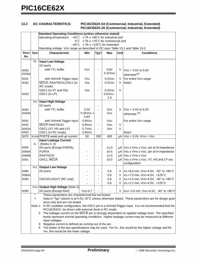
PIC16CE62X
62X.bk Page 84 Tuesday, March 10, 1998 3:40 PM
13.2 DC CHARACTERISTICS: PIC16CE62X-04 (Commercial, Industrial, Extended)
PIC16CE62X-20 (Commercial, Industrial, Extended)
Standard Operating Conditions (unless otherwise stated)Operating temperature –40˚C ≤ TA ≤ +85˚C for industrial and
0˚C ≤ TA ≤ +70˚C for commercial and–40˚C ≤ TA ≤ +125˚C for extended
Operating voltage VDD range as described in DC spec Table 13-1 and Table 13-2
Parm No.
Sym Characteristic Min Typ† Max Unit Conditions
VIL Input Low VoltageI/O ports
D030D030A
with TTL buffer VSS - 0.8V0.15VDD
V VDD = 4.5V to 5.5V
otherwise(4)
D031 with Schmitt Trigger input VSS 0.2VDD V For entire VDD rangeD032 MCLR, RA4/T0CKI,OSC1 (in
RC mode)Vss - 0.2VDD V Note1
D033OSC1 (in XT and HS) OSC1 (in LP)
Vss - 0.3VDD
0.6VDD - 1.0
V
VIH Input High VoltageI/O ports -
D040D040A
with TTL buffer 2.0V 0.25VDD +
0.8V
- VDD
VDD
V VDD = 4.5V to 5.5V
otherwise (4)
D041 with Schmitt Trigger input 0.8VDD VDD For entire VDD rangeD042 MCLR RA4/T0CKI 0.8VDD - VDD VD042AD043
OSC1 (XT, HS and LP)OSC1 (in RC mode)
0.7VDD
0.9VDD
- VDD VNote1
D070 IPURB PORTB weak pull-up current 50 200 400 µA VDD = 5.0V, VPIN = VSS
D060IIL
Input Leakage Current (Notes 2, 3)I/O ports (Except PORTA) ±1.0 µA VSS ≤ VPIN ≤ VDD, pin at hi-impedance
D060A PORTA - - ±0.5 µA Vss ≤ VPIN ≤ VDD, pin at hi-impedanceD060B RA4/T0CKI - - ±1.0 µA Vss ≤ VPIN ≤ VDD
D061 OSC1, MCLR - - ±5.0 µA Vss ≤ VPIN ≤ VDD, XT, HS and LP osc configuration
VOL Output Low VoltageD080 I/O ports - - 0.6 V IOL=8.5 mA, VDD=4.5V, -40° to +85°CD080A - - 0.6 V IOL=7.0 mA, VDD=4.5V, +125°CD083 OSC2/CLKOUT (RC only) - - 0.6 V IOL=1.6 mA, VDD=4.5V, -40° to +85°C
- - 0.6 V IOL=1.2 mA, VDD=4.5V, +125°CVOH Output High Voltage (Note 3)
D090 I/O ports (Except RA4) VDD-0.7 - - V IOH=-3.0 mA, VDD=4.5V, -40° to +85°C* These parameters are characterized but not tested.† Data in “Typ” column is at 5.0V, 25°C unless otherwise stated. These parameters are for design guid-
ance only and are not tested.Note 1: In RC oscillator configuration, the OSC1 pin is a Schmitt Trigger input. It is not recommended that the
PIC16CE62X be driven with external clock in RC mode.2: The leakage current on the MCLR pin is strongly dependent on applied voltage level. The specified
levels represent normal operating conditions. Higher leakage current may be measured at different input voltages.
3: Negative current is defined as coming out of the pin.4: The better of the two specifications may be used. For VIL, this would be the higher voltage and for
VIH, this would be the lower voltage.
DS40182A-page 84 Preliminary 1998 Microchip Technology Inc.


PIC16CE62X
62X.bk Page 86 Tuesday, March 10, 1998 3:40 PM
TABLE 13-2: COMPARATOR SPECIFICATIONS
Operating Conditions: Vdd range as described in Table 12-1, -40°C<TA<+125°C. Current consumption is specified inTable 13-1.
TABLE 13-3: VOLTAGE REFERENCE SPECIFICATIONS
Operating Conditions:Vdd range as described in Table 12-1, -40°C<TA<+125°C. Current consumption is specified inTable 13-1.
Param No. Characteristics Sym Min Typ Max Units Comments
D300 Input offset voltage VIOFF ± 5.0 ± 10 mV
D301 Input common mode voltage VICM 0 VDD - 1.5 V
D302 CMRR CMRR +55* db
300 Response Time(1) TRESP 150* 400* ns PIC16CE62X
301 Comparator Mode Change to Output Valid
TMC2OV 10* µs
* These parameters are characterized but not tested.Note 1: Response time measured with one comparator input at (VDD - 1.5)/2 while the other input transitions from
VSS to VDD.
Param No.
Characteristics Sym Min Typ Max Units Comments
D310 Resolution VRES VDD/24 VDD/32 LSB
D311 Absolute Accuracy VRAA +1/4+1/2
LSBLSB
Low Range (VRR=1)High Range (VRR=0)
D312 Unit Resistor Value (R) VRUR 2K* Ω Figure 9-2
310 Settling Time(1) TSET 10* µs
* These parameters are characterized but not tested.Note 1: Settling time measured while VRR = 1 and VR<3:0> transitions from 0000 to 1111.
DS40182A-page 86 Preliminary 1998 Microchip Technology Inc.


PIC16CE62X
62X.bk Page 88 Tuesday, March 10, 1998 3:40 PM
13.4 Timing Diagrams and Specifications
FIGURE 13-2: EXTERNAL CLOCK TIMING
TABLE 13-4: EXTERNAL CLOCK TIMING REQUIREMENTS
Parameter No.
Sym Characteristic Min Typ† Max Units Conditions
Fos External CLKIN Frequency (Note 1)
DC — 4 MHz XT and RC osc mode, VDD=5.0V
DC — 20 MHz HS osc mode
DC — 200 kHz LP osc mode
Oscillator Frequency (Note 1)
DC — 4 MHz RC osc mode, VDD=5.0V
0.1 — 4 MHz XT osc mode
1 — 20 MHz HS osc mode
DC – 200 kHz LP osc mode
1 Tosc External CLKIN Period(Note 1)
250 — — ns XT and RC osc mode
50 — — ns HS osc mode
5 — — µs LP osc mode
Oscillator Period(Note 1)
250 — — ns RC osc mode
250 — 10,000 ns XT osc mode
50 — 1,000 ns HS osc mode
5 — — µs LP osc mode
2 TCY Instruction Cycle Time (Note 1) 1.0 Fosc/4 DC µs TCYS=FOSC/43* TosL,
TosHExternal Clock in (OSC1) High or Low Time
100* — — ns XT oscillator, TOSC L/H duty cycle
2* — — µs LP oscillator, TOSC L/H duty cycle
20* — — ns HS oscillator, TOSC L/H duty cycle
4* TosR,TosF
External Clock in (OSC1) Rise or Fall Time
25* — — ns XT oscillator
50* — — ns LP oscillator
15* — — ns HS oscillator
* These parameters are characterized but not tested.† Data in "Typ" column is at 5.0V, 25°C unless otherwise stated. These parameters are for design guidance
only and are not tested.Note 1: Instruction cycle period (TCY) equals four times the input oscillator time-base period. All specified values are
based on characterization data for that particular oscillator type under standard operating conditions with the device executing code. Exceeding these specified limits may result in an unstable oscillator operation and/or higher than expected current consumption. All devices are tested to operate at "min." values with an exter-nal clock applied to the OSC1 pin.When an external clock input is used, the "Max." cycle time limit is "DC" (no clock) for all devices.
OSC1
CLKOUT
Q4 Q1 Q2 Q3 Q4 Q1
1 3 34 4
2
DS40182A-page 88 Preliminary 1998 Microchip Technology Inc.


PIC16CE62X
62X.bk Page 90 Tuesday, March 10, 1998 3:40 PM
FIGURE 13-4: RESET, WATCHDOG TIMER, OSCILLATOR START-UP TIMER AND POWER-UP TIMER TIMING
FIGURE 13-5: BROWN-OUT RESET TIMING
TABLE 13-6: RESET, WATCHDOG TIMER, OSCILLATOR START-UP TIMER AND POWER-UP TIMER REQUIREMENTS
Parameter No.
Sym Characteristic Min Typ† Max Units Conditions
30 TmcL MCLR Pulse Width (low) 2000 — — ns -40° to +85°C
31 Twdt Watchdog Timer Time-out Period (No Prescaler)
7* 18 33* ms VDD = 5.0V, -40° to +85°C
32 Tost Oscillation Start-up Timer Period — 1024 TOSC — — TOSC = OSC1 period
33 Tpwrt Power-up Timer Period 28* 72 132* ms VDD = 5.0V, -40° to +85°C
34 TIOZ I/O hi-impedance from MCLR low — 2.0 µs
35 TBOR Brown-out Reset Pulse Width 100* — — µs 3.7V ≤ VDD ≤ 4.3V
* These parameters are characterized but not tested.† Data in "Typ" column is at 5.0V, 25°C unless otherwise stated. These parameters are for design guidance
only and are not tested.
VDD
MCLR
InternalPOR
PWRTTimeout
OSCTimeout
InternalRESET
WatchdogTimer
RESET
33
32
30
3134
I/O Pins
34
VDD BVDD
35
DS40182A-page 90 Preliminary 1998 Microchip Technology Inc.

PIC16CE62X
62X.bk Page 91 Tuesday, March 10, 1998 3:40 PM
FIGURE 13-6: TIMER0 CLOCK TIMING
TABLE 13-7: TIMER0 CLOCK REQUIREMENTS
Parameter No.
Sym Characteristic Min Typ† Max Units Conditions
40 Tt0H T0CKI High Pulse Width No Prescaler 0.5 TCY + 20* — — ns
With Prescaler 10* — — ns
41 Tt0L T0CKI Low Pulse Width No Prescaler 0.5 TCY + 20* — — ns
With Prescaler 10* — — ns
42 Tt0P T0CKI Period TCY + 40*N
— — ns N = prescale value (1, 2, 4, ..., 256)
* These parameters are characterized but not tested.† Data in "Typ" column is at 5.0V, 25°C unless otherwise stated. These parameters are for design guidance
only and are not tested.
41
42
40
RA4/T0CKI
TMR0
1998 Microchip Technology Inc. Preliminary DS40182A-page 91

PIC16CE62X
62X.bk Page 92 Tuesday, March 10, 1998 3:40 PM
13.5 EEPROM Timing
TABLE 13-8: AC CHARACTERISTICS
FIGURE 13-7: BUS TIMING DATA
Parameter Symbol
STANDARD MODE
Vcc = 4.5 - 5.5VFAST MODE Units Remarks
Min. Max. Min. Max.
Clock frequency FCLK — 100 — 400 kHzClock high time THIGH 4000 — 600 — nsClock low time TLOW 4700 — 1300 — nsSDA and SCL rise time TR — 1000 — 300 ns (Note 1)SDA and SCL fall time TF — 300 — 300 ns (Note 1)START condition hold time THD:STA 4000 — 600 — ns After this period the first
clock pulse is generatedSTART condition setup time TSU:STA 4700 — 600 — ns Only relevant for repeated
START conditionData input hold time THD:DAT 0 — 0 — ns (Note 2)Data input setup time TSU:DAT 250 — 100 — nsSTOP condition setup time TSU:STO 4000 — 600 — nsOutput valid from clock TAA — 3500 — 900 ns (Note 2)Bus free time TBUF 4700 — 1300 — ns Time the bus must be free
before a new transmission can start
Output fall time from VIH
minimum to VIL maximumTOF — 250 20 +0.1
CB250 ns (Note 1), CB ≤ 100 pF
Input filter spike suppression(SDA and SCL pins)
TSP — 50 — 50 ns (Note 3)
Write cycle time TWR — 10 — 10 ms Byte or Page modeEndurance
—10M1M
— 10M1M
— cycles25°C, Vcc = 5.0V, Block Mode (Note 4)
Note 1: Not 100% tested. CB = total capacitance of one bus line in pF.2: As a transmitter, the device must provide an internal minimum delay time to bridge the undefined region
(minimum 300 ns) of the falling edge of SCL to avoid unintended generation of START or STOP conditions.3: The combined TSP and VHYS specifications are due to new Schmitt trigger inputs which provide improved
noise spike suppression. This eliminates the need for a TI specification for standard operation.4: This parameter is not tested but guaranteed by characterization. For endurance estimates in a specific appli-
cation, please consult the Total Endurance Model which can be obtained on our website.
SCL
SDAIN
SDAOUT
THD:STA
TSU:STA
TF
THIGH
TR
TSU:STOTSU:DATTHD:DAT
TBUFTAATHD:STATAA
TSP
TLOW
DS40182A-page 92 Preliminary 1998 Microchip Technology Inc.

PIC16CE62X
62X.bk Page 93 Tuesday, March 10, 1998 3:40 PM
14.0 PACKAGING INFORMATIONPackage Type: K04-010 18-Lead Ceramic Dual In-line with Window (JW) – 300 mil
* Controlling Parameter.
n
2
1
R
MIN
Window LengthWindow WidthOverall Row SpacingRadius to Radius WidthPackage WidthPackage LengthTip to Seating PlaneBase to Seating PlaneTop of Lead to Seating PlaneTop to Seating PlaneLead ThicknessShoulder RadiusUpper Lead WidthLower Lead Width
Number of PinsPCB Row SpacingDimension Limits
Pitch
Units
eB
W2W1
L
EE1
D
A1A2
A
B
cRB1
np
0.15
7.247.87
0.763.334.830.300.381.520.532.59
0.2000.1400.3850.2700.2980.9000.1380.0230.1110.183
0.1900.1300.345
0.125
0.2550.2850.880
0.0150.0910.175
0.2100.1500.425
0.150
0.2850.3100.920
0.0300.1310.190
0.0100.0130.0550.0190.100
0.300NOM
0.016
0.0080.0100.050
0.098
INCHES*MAX
18
0.021
0.0120.0150.060
0.102
22.86
0.190.138.766.487.24
22.353.180.002.314.45
0.20.149.78 10.80
0.21
3.49
6.867.56
0.572.824.64
3.8123.37
NOMMILLIMETERS
MIN
0.200.251.270.412.49
MAX
0.47
0.250.321.40
2.5418
7.62
DW2
E
W1
c
eB
E1
p
L
A1
B
B1
A
A2
1998 Microchip Technology Inc. Preliminary DS40182A-page 93

PIC16CE62X
62X.bk Page 94 Tuesday, March 10, 1998 3:40 PM
Package Type: K04-007 18-Lead Plastic Dual In-line (P) – 300 mil
* Controlling Parameter.† Dimension “B1” does not include dam-bar protrusions. Dam-bar protrusions shall not exceed 0.003”
(0.076 mm) per side or 0.006” (0.152 mm) more than dimension “B1.”‡ Dimensions “D” and “E” do not include mold flash or protrusions. Mold flash or protrusions shall not
exceed 0.010” (0.254 mm) per side or 0.020” (0.508 mm) more than dimensions “D” or “E.”
Units INCHES* MILLIMETERSDimension Limits MIN NOM MAX MIN NOM MAXPCB Row Spacing 0.300 7.62Number of Pins n 18 18Pitch p 0.100 2.54Lower Lead Width B 0.013 0.018 0.023 0.33 0.46 0.58Upper Lead Width B1† 0.055 0.060 0.065 1.40 1.52 1.65Shoulder Radius R 0.000 0.005 0.010 0.00 0.13 0.25Lead Thickness c 0.005 0.010 0.015 0.13 0.25 0.38Top to Seating Plane A 0.110 0.155 0.155 2.79 3.94 3.94Top of Lead to Seating Plane A1 0.075 0.095 0.115 1.91 2.41 2.92Base to Seating Plane A2 0.000 0.020 0.020 0.00 0.51 0.51Tip to Seating Plane L 0.125 0.130 0.135 3.18 3.30 3.43Package Length D‡ 0.890 0.895 0.900 22.61 22.73 22.86Molded Package Width E‡ 0.245 0.255 0.265 6.22 6.48 6.73Radius to Radius Width E1 0.230 0.250 0.270 5.84 6.35 6.86Overall Row Spacing eB 0.310 0.349 0.387 7.87 8.85 9.83Mold Draft Angle Top α 5 10 15 5 10 15Mold Draft Angle Bottom β 5 10 15 5 10 15
R
n
2
1
D
E
c
eB
β
E1
α
p
A1
L
B1
B
A
A2
DS40182A-page 94 Preliminary 1998 Microchip Technology Inc.
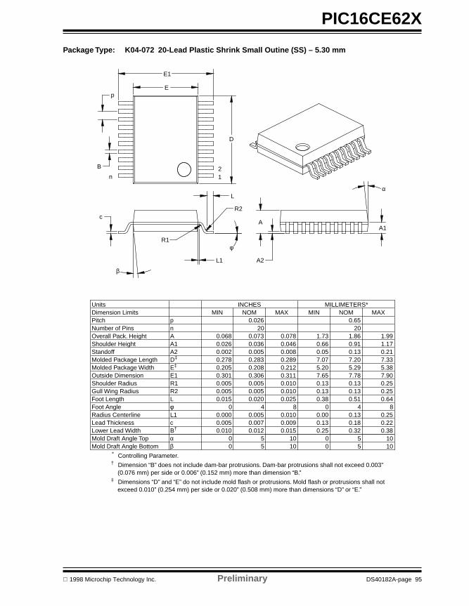
PIC16CE62X
62X.bk Page 95 Tuesday, March 10, 1998 3:40 PM
Package Type: K04-072 20-Lead Plastic Shrink Small Outine (SS) – 5.30 mm
MINpPitch
Mold Draft Angle BottomMold Draft Angle TopLower Lead Width
Radius Centerline
Gull Wing RadiusShoulder RadiusOutside DimensionMolded Package WidthMolded Package Length
Shoulder HeightOverall Pack. Height
Lead Thickness
Foot AngleFoot Length
Standoff
Number of Pins
βα
c
φ
A2A1An
E1
B†
L1
R2L
R1
E‡D‡
Dimension LimitsUnits
0.650.026
8
00
55 10
100.0120.0070.005
0.0200.0050.0050.3060.2080.2830.0050.0360.073
20
0.301
0
0.0100.0050.000
0.0150.0050.005
0.2050.2780.0020.0260.068
0.311
0.0150.0090.010
0.0250.0100.010
4 8
0.2120.2890.0080.0460.078
00 5
5 1010
7.65
0.250.130.00
0.380.130.13
0
5.207.070.050.661.73
7.907.78
4
0.320.180.13
0.130.51
0.13
0.380.220.25
0.250.64
0.25
5.297.200.13
201.860.91
5.387.330.21
1.991.17
NOMINCHES
MAX NOMMILLIMETERS*
MIN MAX
n 12
R1
R2
D
p
B
E1
E
L1
L
c
β
φ
α
A1A
A2
* Controlling Parameter.† Dimension “B” does not include dam-bar protrusions. Dam-bar protrusions shall not exceed 0.003”
(0.076 mm) per side or 0.006” (0.152 mm) more than dimension “B.”‡ Dimensions “D” and “E” do not include mold flash or protrusions. Mold flash or protrusions shall not
exceed 0.010” (0.254 mm) per side or 0.020” (0.508 mm) more than dimensions “D” or “E.”
1998 Microchip Technology Inc. Preliminary DS40182A-page 95
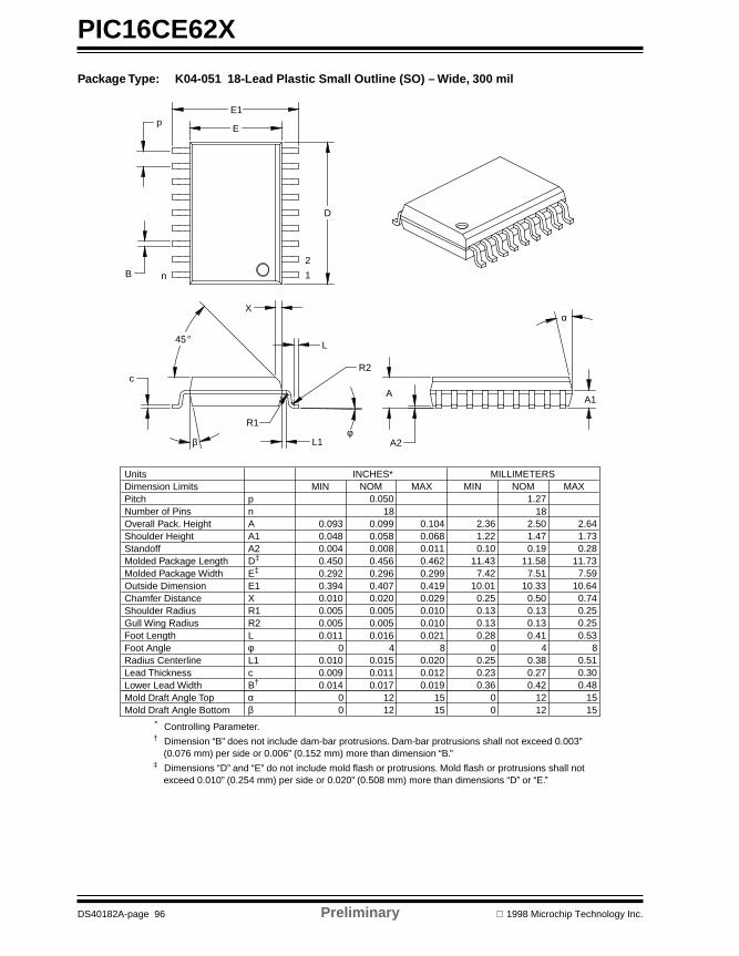
PIC16CE62X
62X.bk Page 96 Tuesday, March 10, 1998 3:40 PM
Package Type: K04-051 18-Lead Plastic Small Outline (SO) – Wide, 300 mil
0.0140.0090.010
0.0110.0050.0050.0100.3940.2920.4500.0040.0480.093
MIN
nNumber of Pins
Mold Draft Angle BottomMold Draft Angle TopLower Lead Width
Chamfer DistanceOutside DimensionMolded Package WidthMolded Package Length
Overall Pack. Height
Lead ThicknessRadius CenterlineFoot AngleFoot LengthGull Wing RadiusShoulder Radius
StandoffShoulder Height
βα
R2R1
E1
A2A1
X
φ
B†cL1
L
E‡D‡
A
Dimension LimitsPitch
Units
p1818
00
1212
1515
4
0.020
0
0.0170.0110.015
0.0160.0050.005
0.4070.2960.4560.0080.0580.099
0.029
0.0190.0120.020
0.0210.0100.010
8
0.4190.2990.4620.0110.0680.104
00
1212
1515
0.420.270.38
0.410.130.130.50
10.337.51
11.580.191.472.50
0.25
0
0.360.230.25
0.280.130.13
10.017.42
11.430.101.222.36
0.74
4 8
0.480.300.51
0.530.250.25
10.647.59
11.730.281.732.64
INCHES*
0.050NOM MAX
1.27
MILLIMETERSMIN NOM MAX
n
2
1
R2
R1
L1
L
β
c
φ
X
45 °
D
p
B
E
E1
α
A1
A2
A
* Controlling Parameter.† Dimension “B” does not include dam-bar protrusions. Dam-bar protrusions shall not exceed 0.003”
(0.076 mm) per side or 0.006” (0.152 mm) more than dimension “B.”‡ Dimensions “D” and “E” do not include mold flash or protrusions. Mold flash or protrusions shall not
exceed 0.010” (0.254 mm) per side or 0.020” (0.508 mm) more than dimensions “D” or “E.”
DS40182A-page 96 Preliminary 1998 Microchip Technology Inc.

PIC16CE62X
62X.bk Page 97 Tuesday, March 10, 1998 3:40 PM
14.1 Package Marking Information
Legend: MM...M Microchip part number informationXX...X Customer specific information*AA Year code (last 2 digits of calendar year)BB Week code (week of January 1 is week ‘01’)C Facility code of the plant at which wafer is manufactured
O = Outside VendorC = 5” Line S = 6” LineH = 8” Line
D Mask revision numberE Assembly code of the plant or country of origin in which
part was assembled
Note: In the event the full Microchip part number cannot be marked on one line,it will be carried over to the next line thus limiting the number of availablecharacters for customer specific information.
* Standard OTP marking consists of Microchip part number, year code, weekcode, facility code, mask rev#, and assembly code. For OTP marking beyondthis, certain price adders apply. Please check with your Microchip Sales Office.For QTP devices, any special marking adders are included in QTP price.
XXXXXXXXXXXXXXXXAABBCDE
18-Lead CERDIP Windowed
18-Lead SOIC (.300")
XXXXXXXXXXXX
AABBCDEXXXXXXXXXXXX
XXXXXXXXXXXX
XXXXXXXXXXXXXXXXXXXXXXXXXXXXXXXX
AABBCDE
18-Lead PDIP
16CE625/JW9807 CBA
Example
Example
-04I/S0218
9807 CDK
PIC16CE625
PIC16CE625-04I/P423
9807CDK
Example
XXXXXXXXXX
AABBCDEXXXXXXXXXX
20-Lead SSOP
PIC16CE625
9807 CBP-04I/218
Example
1998 Microchip Technology Inc. Preliminary DS40182A-page 97

PIC16CE62X
62X.bk Page 98 Tuesday, March 10, 1998 3:40 PM
NOTES:
DS40182A-page 98 Preliminary 1998 Microchip Technology Inc.

PIC16CE62X
62X.bk Page 99 Tuesday, March 10, 1998 3:40 PM
APPENDIX A: CODE FOR ACCESSING EEPROM DATA MEMORY
To be determined. Please check our web site atwww.microchip.com for code availability.
1998 Microchip Technology Inc. Prelimin
ary DS40182A-page 99
PIC16CE62X
62X.bk Page 100 Tuesday, March 10, 1998 3:40 PM
NOTES:
DS40182A-page 100 Prelimin
ary 1998 Microchip Technology Inc.
PIC16CE62X
62X.bk Page 101 Tuesday, March 10, 1998 3:40 PM
INDEXAADDLW Instruction ............................................................. 67ADDWF Instruction ............................................................. 67ANDLW Instruction ............................................................. 67ANDWF Instruction ............................................................. 67Architectural Overview .......................................................... 7Assembler
MPASM Assembler..................................................... 78
BBCF Instruction ................................................................... 68Block Diagram
TIMER0....................................................................... 35TMR0/WDT PRESCALER .......................................... 38
Brown-Out Detect (BOD) .................................................... 54BSF Instruction ................................................................... 68BTFSC Instruction............................................................... 68BTFSS Instruction............................................................... 69
CCALL Instruction ................................................................. 69Clocking Scheme/Instruction Cycle .................................... 10CLRF Instruction ................................................................. 69CLRW Instruction................................................................ 69CLRWDT Instruction ........................................................... 70CMCON Register ................................................................ 41Code Protection .................................................................. 64COMF Instruction................................................................ 70Comparator Configuration................................................... 42Comparator Interrupts......................................................... 45Comparator Module ............................................................ 41Comparator Operation ........................................................ 43Comparator Reference ....................................................... 43Configuration Bits................................................................ 50Configuring the Voltage Reference..................................... 47Crystal Operation ................................................................ 51
DData Memory Organization ................................................. 12DECF Instruction................................................................. 70DECFSZ Instruction ............................................................ 70Development Support ......................................................... 77Development Tools ............................................................. 77
EEEPROM Peripheral Operation .......................................... 29External Crystal Oscillator Circuit ....................................... 52
FFuzzy Logic Dev. System (fuzzyTECH -MP) .................... 79
GGeneral purpose Register File ............................................ 12GOTO Instruction................................................................ 71
II/O Ports.............................................................................. 23I/O Programming Considerations........................................ 28ICEPIC Low-Cost PIC16CXXX In-Circuit Emulator ............ 77ID Locations ........................................................................ 64INCF Instruction .................................................................. 71INCFSZ Instruction ............................................................. 71In-Circuit Serial Programming............................................. 64Indirect Addressing, INDF and FSR Registers ................... 21Instruction Flow/Pipelining .................................................. 10Instruction Set
ADDLW....................................................................... 67ADDWF....................................................................... 67
ANDLW....................................................................... 67ANDWF ...................................................................... 67BCF ............................................................................ 68BSF............................................................................. 68BTFSC........................................................................ 68BTFSS........................................................................ 69CALL........................................................................... 69CLRF .......................................................................... 69CLRW......................................................................... 69CLRWDT .................................................................... 70COMF......................................................................... 70DECF.......................................................................... 70DECFSZ ..................................................................... 70GOTO......................................................................... 71INCF ........................................................................... 71INCFSZ....................................................................... 71IORLW........................................................................ 71IORWF........................................................................ 72MOVF ......................................................................... 72MOVLW...................................................................... 72MOVWF...................................................................... 72NOP............................................................................ 73OPTION...................................................................... 73RETFIE....................................................................... 73RETLW....................................................................... 73RETURN..................................................................... 74RLF............................................................................. 74RRF ............................................................................ 74SLEEP........................................................................ 74SUBLW....................................................................... 75SUBWF....................................................................... 75SWAPF....................................................................... 76TRIS ........................................................................... 76XORLW ...................................................................... 76XORWF ...................................................................... 76
Instruction Set Summary .................................................... 65INT Interrupt ....................................................................... 60INTCON Register ............................................................... 17Interrupts ............................................................................ 59IORLW Instruction .............................................................. 71IORWF Instruction .............................................................. 72
KKeeLoq Evaluation and Programming Tools ................... 79
MMOVF Instruction................................................................ 72MOVLW Instruction ............................................................ 72MOVWF Instruction ............................................................ 72MP-DriveWay™ - Application Code Generator .................. 79MPLAB C............................................................................ 79MPLAB Integrated Development Environment Software.... 78
NNOP Instruction .................................................................. 73
OOne-Time-Programmable (OTP) Devices .............................5OPTION Instruction ............................................................ 73OPTION Register ............................................................... 16Oscillator Configurations .................................................... 51Oscillator Start-up Timer (OST).......................................... 54
PPackage Marking Information............................................. 97Packaging Information........................................................ 93PCL and PCLATH .............................................................. 20PCON Register ................................................................... 19PICDEM-1 Low-Cost PICmicro Demo Board ..................... 78
1998 Microchip Technology Inc. Preliminary DS40182A-page 101

PIC16CE62X
62X.bk Page 102 Tuesday, March 10, 1998 3:40 PM
PICDEM-2 Low-Cost PIC16CXX Demo Board ................... 78PICDEM-3 Low-Cost PIC16CXXX Demo Board................. 78PICMASTER In-Circuit Emulator...................................... 77PICSTART Plus Entry Level Development System ......... 77PIE1 Register ...................................................................... 18Pinout Description ................................................................. 9PIR1 Register...................................................................... 18Port RB Interrupt ................................................................. 60PORTA................................................................................ 23PORTB................................................................................ 26Power Control/Status Register (PCON) .............................. 55Power-Down Mode (SLEEP)............................................... 63Power-On Reset (POR) ...................................................... 54Power-up Timer (PWRT)..................................................... 54Prescaler ............................................................................. 38PRO MATE II Universal Programmer............................... 77Program Memory Organization ........................................... 11
QQuick-Turnaround-Production (QTP) Devices ...................... 5
RRC Oscillator ....................................................................... 52Reset................................................................................... 53RETFIE Instruction.............................................................. 73RETLW Instruction .............................................................. 73RETURN Instruction............................................................ 74RLF Instruction.................................................................... 74RRF Instruction ................................................................... 74
SSEEVAL Evaluation and Programming System............... 79Serialized Quick-Turnaround-Production (SQTP) Devices ... 5SLEEP Instruction ............................................................... 74Software Simulator (MPLAB-SIM)....................................... 79Special Features of the CPU............................................... 49Special Function Registers ................................................. 14Stack ................................................................................... 20Status Register.................................................................... 15SUBLW Instruction.............................................................. 75SUBWF Instruction.............................................................. 75SWAPF Instruction.............................................................. 76
TTimer0
TIMER0....................................................................... 35TIMER0 (TMR0) Interrupt ........................................... 35TIMER0 (TMR0) Module............................................. 35TMR0 with External Clock........................................... 37
Timer1Switching Prescaler Assignment................................. 39
Timing Diagrams and Specifications................................... 88TMR0 Interrupt .................................................................... 60TRIS Instruction .................................................................. 76TRISA.................................................................................. 23TRISB.................................................................................. 26
VVoltage Reference Module.................................................. 47VRCON Register................................................................. 47
WWatchdog Timer (WDT) ...................................................... 61
XXORLW Instruction ............................................................. 76XORWF Instruction ............................................................. 76
DS40182A-page 102 Preliminary 1998 Microchip Technology Inc.

PIC16CE62X
62X.bk Page 103 Tuesday, March 10, 1998 3:40 PM
ON-LINE SUPPORT
Microchip provides on-line support on the MicrochipWorld Wide Web (WWW) site.
The web site is used by Microchip as a means to makefiles and information easily available to customers. Toview the site, the user must have access to the Internetand a web browser, such as Netscape or MicrosoftExplorer. Files are also available for FTP downloadfrom our FTP site.
Connecting to the Microchip Internet Web Site
The Microchip web site is available by using yourfavorite Internet browser to attach to:
www.microchip.com
The file transfer site is available by using an FTP ser-vice to connect to:
ftp://ftp.futureone.com/pub/microchip
The web site and file transfer site provide a variety ofservices. Users may download files for the latestDevelopment Tools, Data Sheets, Application Notes,User's Guides, Articles and Sample Programs. A vari-ety of Microchip specific business information is alsoavailable, including listings of Microchip sales offices,distributors and factory representatives. Other dataavailable for consideration is:
• Latest Microchip Press Releases• Technical Support Section with Frequently Asked
Questions • Design Tips• Device Errata• Job Postings• Microchip Consultant Program Member Listing• Links to other useful web sites related to
Microchip Products• Conferences for products, Development Systems,
technical information and more• Listing of seminars and events
1998 Microchip Technology Inc.
Systems Information and Upgrade Hot Line
The Systems Information and Upgrade Line providessystem users a listing of the latest versions of all ofMicrochip's development systems software products.Plus, this line provides information on how customerscan receive any currently available upgrade kits.TheHot Line Numbers are:
1-800-755-2345 for U.S. and most of Canada, and
1-602-786-7302 for the rest of the world.
Trademarks: The Microchip name, logo, PIC, PICSTART, PICMASTER and PRO MATE are registered trademarks of Microchip Technology Incorporated in the U.S.A. and other countries. PICmicro, FlexROM, MPLAB and fuzzy-LAB are trademarks and SQTP is a service mark of Micro-chip in the U.S.A.
All other trademarks mentioned herein are the property of their respective companies.
980106
DS40182A-page 103

PIC16CE62X
62X.bk Page 104 Tuesday, March 10, 1998 3:40 PM
READER RESPONSE
It is our intention to provide you with the best documentation possible to ensure successful use of your Microchip prod-uct. If you wish to provide your comments on organization, clarity, subject matter, and ways in which our documentationcan better serve you, please FAX your comments to the Technical Publications Manager at (602) 786-7578.
Please list the following information, and use this outline to provide us with your comments about this Data Sheet.
1. What are the best features of this document?
2. How does this document meet your hardware and software development needs?
3. Do you find the organization of this data sheet easy to follow? If not, why?
4. What additions to the data sheet do you think would enhance the structure and subject?
5. What deletions from the data sheet could be made without affecting the overall usefulness?
6. Is there any incorrect or misleading information (what and where)?
7. How would you improve this document?
8. How would you improve our software, systems, and silicon products?
To: Technical Publications Manager
RE: Reader Response
Total Pages Sent
From: Name
Company
Address
City / State / ZIP / Country
Telephone: (_______) _________ - _________
Application (optional):
Would you like a reply? Y N
Device: Literature Number:
Questions:
FAX: (______) _________ - _________
DS40182APIC16CE62X
DS40182A-page 104 1998 Microchip Technology Inc.

PIC16CE62X
62X.bk Page 105 Tuesday, March 10, 1998 3:40 PM
PIC16CE62X PRODUCT IDENTIFICATION SYSTEM
To order or to obtain information, e.g., on pricing or delivery, please use the listed part numbers, and refer to the factory or the listedsales offices.
* JW Devices are UV erasable and can be programmed to any device configuration. JW Devices meet the electrical requirement ofeach oscillator type.
Sales and Support
Products supported by a preliminary Data Sheet may possibly have an errata sheet describing minor operational differences and recommended workarounds. To determine if an errata sheet exists for a particular device, please contact one of the following:
1. Your local Microchip sales office.
2. The Microchip Corporate Literature Center U.S. FAX: (602) 786-7277
Please specify which device, revision of silicon and Data Sheet (include Literature #) you are using.
For latest version information and upgrade kits for Microchip Development Tools, please call 1-800-755-2345 or 1-602-786-7302.
Pattern: 3-Digit Pattern Code for QTP (blank otherwise)
Package: P = PDIPSO = SOIC (Gull Wing, 300 mil body)SS = SSOP (209 mil)JW* = Windowed CERDIP
Temperature - = 0˚C to +70˚CRange: I = –40˚C to +85˚C
E = –40˚C to +125˚C
Frequency 04 = 200kHz (LP osc)Range: 04 = 4 MHz (XT and RC osc)
20 = 20 MHz (HS osc)
Device: PIC16CE62X :VDD range 3.0V to 5.5VPIC16CE62XT:VDD range 3.0V to 5.5V (Tape and Reel)
Examples:a) PIC16CE623-04/P301 =
Commercial temp., PDIP pack-age, 4 MHz, normal VDD limits, QTP pattern #301.
b) PIC16CE623-04I/SO = Industrial temp., SOIC pack-age, 4MHz, industrial VDD lim-its.
PART NO. -XX X /XX XXX
1998 Microchip Technology Inc. Preliminary DS40182A-page 105

PIC16CE62X
62X.bk Page 106 Tuesday, March 10, 1998 3:40 PM
NOTES:
DS40182A-page 106 Prelimin
ary 1998 Microchip Technology Inc.
PIC16CE62X
62X.bk Page 107 Tuesday, March 10, 1998 3:40 PM
NOTES:
1998 Microchip Technology Inc. Prelimin
ary DS40182A-page 107