quickusb user guide v2.11.41
DESCRIPTION
quick usb user guideTRANSCRIPT

User Guide
6489 Calle Real, Suite E Goleta, CA 93117 Voice (805) 683-6469 Fax (805) 683-4833 Toll Free (800) 224-1633 Web Site www.bitwisesys.comInformation [email protected] Support [email protected]

QuickUSB User Guide Version 2.11.41 April 24, 2007 Copyright © 2005, 2006, 2007 Bitwise Systems. All rights reserved. This document contains confidential information and trade secrets of Bitwise Systems, and is protected by United States and international copyright laws. Use, disclosure, or reproduction is prohibited without the prior express written permission of Bitwise Systems, except as agreed in the License Agreement. Use, duplication or disclosure by the U.S. Government is subject to restrictions as provided in DFARS 227.7202-1(a) and 227.7202-3(a) (1998), and FAR 12.212, as applicable.
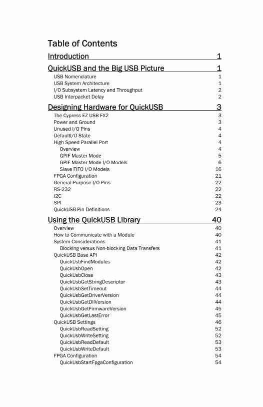
Table of Contents Introduction 1 QuickUSB and the Big USB Picture 1
USB Nomenclature 1 USB System Architecture 1 I/O Subsystem Latency and Throughput 2 USB Interpacket Delay 2
Designing Hardware for QuickUSB 3 The Cypress EZ USB FX2 3 Power and Ground 3 Unused I/O Pins 4 DefaultI/O State 4 High Speed Parallel Port 4
Overview 4 GPIF Master Mode 5 GPIF Master Mode I/O Models 6 Slave FIFO I/O Models 16
FPGA Configuration 21 General-Purpose I/O Pins 22 RS-232 22 I2C 22 SPI 23 QuickUSB Pin Definitions 24
Using the QuickUSB Library 40 Overview 40 How to Communicate with a Module 40 System Considerations 41
Blocking versus Non-blocking Data Transfers 41 QuickUSB Base API 42
QuickUsbFindModules 42 QuickUsbOpen 42 QuickUsbClose 43 QuickUsbGetStringDescriptor 43 QuickUsbSetTimeout 44 QuickUsbGetDriverVersion 44 QuickUsbGetDllVersion 44 QuickUsbGetFirmwareVersion 45 QuickUsbGetLastError 45
QuickUSB Settings 46 QuickUsbReadSetting 52 QuickUsbWriteSetting 52 QuickUsbReadDefault 53 QuickUsbWriteDefault 53
FPGA Configuration 54 QuickUsbStartFpgaConfiguration 54

QuickUsbWriteFpgaData 55 QuickUsbIsFpgaConfigured 55
High-Speed Parallel Port 56 QuickUsbReadCommand 56 QuickUsbWriteCommand 57 QuickUsbReadData 58 QuickUsbWriteData 59 QuickUsbReadDataAsync 60 QuickUsbWriteDataAsync 61 QuickUsbAsyncWait 62
General-Purpose I/O 63 QuickUsbReadPortDir 63 QuickUsbWritePortDir 63 QuickUsbReadPort 64 QuickUsbWritePort 64
RS-232 65 QuickUsbSetRs232BaudRate 65 QuickUsbGetNumRS232 65 QuickUsbFlushRS232 66 QuickUsbReadRS232 66 QuickUsbWriteRS232 67
I2C-Compatible Port 68 QuickUsbReadI2c 68 QuickUsbWriteI2c 68
SPI-Compatible Port 69 QuickUsbReadSpi 69 QuickUsbWriteSpi 69 QuickUsbWriteReadSpi 70
Index 71
Introduction
Introduction Thank you for choosing QuickUSB®. QuickUSB makes your product a well-connected USB device quickly and with a minimum of hassle. Not only is QuickUSB a quick way to get connected to USB, it also offers great Hi-Speed USB 2.0 performance with a wide variety of target interface options.
We hope this guide will answer all of your questions about QuickUSB. However, if you have a question that you cannot find an answer for in this guide, please check the web site at www.quickusb.com and please use the QuickUSB online support forum. Our support team will do our best get you the answer you need.
QuickUSB and the Big USB Picture Please take some time to understand the big picture as it relates to USB connections. USB has gained the success it has because it is a well-designed bus specifically designed to easily, and reliably connect peripherals to a PC. Part of that design defines the relationship between your PC and the device. Although with QuickUSB you do not need to learn the inner workings of USB, you do need to understand the basics of USB. We will explain the basics here and if you want to learn more, you can browse www.usb.org and learn just about everything that there is to know about USB. Just be careful, because you can easily get distracted from what you really need to accomplish.
USB Nomenclature Conveying the big picture requires defining some key words. The first is USB and it is an acronym for Universal Serial Bus. Host means your PC. Device means the QuickUSB module and/or the subsystem you need to connect to the PC. A pipe is a unidirectional virtual connection between a host and the device. Every pipe has a direction attribute of either IN or OUT to indicate the direction of data flow with respect to the host. An endpoint is the device side connection of a pipe. When a device is connected to a host, the host automatically senses this and enumerates the bus to find it.
USB System Architecture The USB is a master/slave bus. This means that the master initiates all traffic on the bus and the slave can only respond to the master. For the USB, the master is the host computer (your PC) and the slave is the device. This master/slave relationship means that interrupts are not possible on the USB. The USB supports a pseudo-interrupt scheme involving low-latency interrupt endpoints so the host can perform low-latency device polling to emulate an interrupt. QuickUSB does not currently support interrupt endpoints.
USB Nomenclature 1
QuickUSB and the Big USB Picture I/O Subsystem Latency and Throughput The period of time between the start of a transfer and the time that it actually occurs is the transfer latency. USB transfer latency is the result of several factors. First is the fact that the USB is a frame oriented bus and that all packets must be scheduled to a timebase of either 1ms (full speed) or 125us (Hi-Speed). Secondly, the operating system generally assesses a software latency penalty when switching from user mode to kernel mode.
Throughput is a measure of data transfer speed and is generally expressed in megabytes per second (MB/s). Transfer latency affects throughput because it increases the amount of time a transfer takes regardless of the connection speed.
However, as the data transfer size becomes larger, the transfer latency becomes a smaller fraction of the total transfer time thereby diminishing its effect. When the transfer size is small, the transfer latency will seriously degrade throughput.
Therefore, for applications that require the highest throughput, transfer sizes of at least 64KB are recommended.
Another way to mitigate transfer latency issues is to minimize the amount of time that the USB subsystem waits to schedule USB packets. You can accomplish this using asynchronous function calls. With asynchronous function calls, the transfer is scheduled when the function is called, but the function returns without waiting for the transfer to complete. Using this mechanism, one can concurrently schedule enough USB transfers to assure that the USB will not idle waiting for data to be transferred to or from your device.
The simplest and most reliable technique for this is to employ multiple transfer buffers and rotate them on an as-needed basis.
USB Interpacket Delay In certain circumstances, the USB target interface bandwidth is greater than the USB bus bandwidth. This is the case with the Cypress EZ-USB FX2LP microcontroller. In word-wide mode, the FX2LP can transfer data at up to 96MB/sec. The maximum theoretical throughput of a Hi-Speed USB 2.0 pipe is 54MB/sec. Because the FX2LP can go faster than the USB pipe, the target interface is subject to periods of bus inactivity (‘gaps’) between data packets. Your system design should take into consideration the strong that there will be gaps between data packets and deal with them accordingly.
2 I/O Subsystem Latency and Throughput

Designing Hardware for QuickUSB
Designing Hardware for QuickUSB Connecting QuickUSB to your hardware is simple. First, decide on the type of connection you need. If you need to transfer large amounts of data very quickly, then you should use the High Speed Parallel Port. If you only need to turn some I/O pins on and off, you can just use the general-purpose I/O pins.
The Cypress EZ USB FX2 QuickUSB is based on the Cypress EZ-USB FX2LP microcontroller. The FX2LP is a powerful, single-chip USB microcontroller that offers an unparalleled capability to interface subsystems to a PC with a high-speed USB 2.0 connection. QuickUSB unleashes the power of the FX2LP to high-level hardware and software designers by abstracting its capabilities as library of dataflow oriented function calls. In addition, chip-specific capabilities are supported via ‘Settings’ that allow the user to customize the behavior of the FX2LP to suit the target application.
Power and Ground QuickUSB supplies unregulated +5V at up to 400 mA max on the VBUS pins to power your circuitry. For modules Rev A1 and above, an FET on the QuickUSB module controls power. Power is off by default and then turned on once the host configures the module. This behavior is required by the USB specification. The QuickUSB module incorporates a current limiting circuit that will shut down the VBUS pins on an over-current condition. In addition the entire module may be powered down by the host or a USB hub if it draws more than the 500 mA allotted by the USB.
If your circuit draws less than 400 mA, you may power it from the unregulated 5V provided on the VBUS pins. However, if your circuit will draw more than 50 mA, you should design your circuit with either a downstream power switch (such as the TPS2051A) or an active high enable logic switched voltage regulator. Connect the enable signal to SW_PG (pin 76). This signal will enable your circuit’s voltage regulator once the VBUS switch is turned on and the output voltage has stabilized to >= 93% of the voltage supplied by the USB. For more information about the QuickUSB VBUS switch, consult the datasheet for the Texas Instruments TPS2150.
If your circuit draws more than 400 mA, do not power it from VBUS. It should be powered with an external power supply and connect the digital ground of your circuit to GND. In this case, you might want to connect an unused I/O pin to the external power supply through a current limiting resistor (10K) so you can read the pin to determine the state of the external power supply.
The Cypress EZ USB FX2 3
Designing Hardware for QuickUSB Unused I/O Pins Some I/O pins are reserved for future use and may be activated by a new version of the module or a new firmware release. Therefore, you must not connect unused QuickUSB I/O pins to any signals or power supplies. DO NOT DIRECTLY GROUND UNUSED QUICKUSB I/O PINS IN YOUR CIRCUIT. You may use a 10k resistor to tie unused pins to a known level, but do not connect them directly.
Default I/O State With QuickUSB Library (including firmware) v2.11 and above, QuickUSB supports non-volatile I/O pin default settings. The default settings are programmed and read using the QuickUsbWriteDefault and QuickUsbReadDefault functions respectively.
High Speed Parallel Port The High-Speed parallel port is a truly outstanding feature of the QuickUSB module. It is the fastest connection on the QuickUSB module and can transfer very large blocks of data to and from your device with ease. It provides both master and slave mode transfers with several types of transfer handshaking models.
Overview The high-speed parallel port (HSPP) is an 8 or 16-bit port that is used to transfer high-speed data between the host PC and your device. The WORDWIDE setting controls the data element width. If WORDWIDE = 1, the transfers are 16-bits wide and if 0, 8-bits wide. For more information about WORDWIDE, see the SETTING_WORDWIDE setting in the ‘Settings’ section of this document. If the HSPP is in 8-bit mode, the upper 8 bits may be used as general purpose I/O.
In addition, there is a 9-bit address bus which increments each time a data element is transferred. The address bus can be set to a fixed address to allow multiple writes to the same address. The address bus can also be disabled and the address bus bits reused as general purpose I/O. See the SETTING_DATAADDRESS setting in the ‘Settings’ section of this manual for more information
There are two modes of HSPP operation, master and slave. The HSPP mode is automatically selected by the QuickUSB firmware, but it may be changed at any time using the SETTING_FIFO_CONFIG setting. Typically, your hardware will be configured for either master or slave mode and the requirements of your application will determine which mode is best for you.
4 Unused I/O Pins
Designing Hardware for QuickUSB
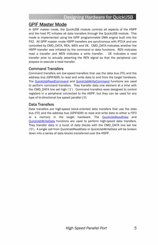
GPIF Master Mode In GPIF master mode, the QuickUSB module controls all aspects of the HSPP and the host PC initiates all data transfers through the QuickUSB module. This mode is implemented using the GPIF programmable DMA engine built into the FX2. All GPIF master mode HSPP transfers are synchronous with IFCLK and are controlled by CMD_DATA, REN, WEN and OE. CMD_DATA indicates whether the HSPP transfer was initiated by the command or data functions. REN indicates read a transfer and WEN indicates a write transfer. OE indicates a read transfer prior to actually asserting the REN signal so that the peripheral can prepare to execute a read transfer.
Command Transfers Command transfers are low-speed transfers that use the data bus (FD) and the address bus (GPIFADR) to read and write data to and from the target hardware. The QuickUsbReadCommand and QuickUsbWriteCommand functions are used to perform command transfers. They transfer data one element at a time with the CMD_DATA line set high (‘1’). Command transfers were designed to control registers in a peripheral connected to the HSPP, but they can be used for any type of bi-directional low speed parallel I/O.
Data Transfers Data transfers are high-speed block-oriented data transfers that use the data bus (FD) and the address bus (GPIFADR) to read and write data to either a FIFO or a memory in the target hardware. The QuickUsbReadData and QuickUsbWriteData functions are used to perform high-speed data transfers. They transfer data in a burst of data blocks with the CMD_DATA line set low (‘0’). A single call from QuickUsbReadData or QuickUsbWriteData will be broken down into a series of data blocks transferred over the HSPP.
High Speed Parallel Port 5

Designing Hardware for QuickUSB
GPIF Master Mode I/O Models The QuickUSB module interfaces to target hardware by implementing a number of I/O models that provide enough flexibility to interface to a wide variety target hardware. The I/O models are selected by reprogramming the firmware of the QuickUSB module using the QuickUSB Programmer. Each firmware load implements a different I/O model. The timing diagrams for each I/O model are given below.
QuickUSB Signal I/O Model Direction FD[15:0] (Word Wide) or FD[7:0] (Byte Wide) All Bidirectional IFCLK All OUT or IN
(Programmable default)
CMD_DATA All OUT REN or nREN All OUT WEN or nWEN All OUT nOE FIFO & Block OUT nEMPTY FIFO & Block IN nFULL FIFO & Block IN
Table 1 – GPIF I/O Connections
GPIF Master Mode Timing Parameters Internally Sourced
IFCLK Externally
Sourced IFCLK Parameter Description Min Max Min Max
Unit
tIFCLK IFCLK Period 20.83 20.83 200 ns
tSRY RDYX to Clock Set-up Time 8.9 2.9 ns
tRYH Clock to RDYX Hold Time 0 3.7 ns
tSGD GPIF Data to Clock Set-up Time 9.2 3.2 ns
tDAH GPIF Data Hold Time 0 4.5 ns
tSGA Clock to GPIF Address Propagation Delay
7.4 11.4 ns
tXGD Clock to GPIF Data Output Propagation Delay
11 15 ns
tXCTL Clock to CTLX Output Propagation Delay
6.7 10.7 ns
Table 2 – GPIF Master Mode Timing Parameters
6 High Speed Parallel Port

Designing Hardware for QuickUSB Simple I/O Model This I/O model performs transfers without regard to the readiness of the target hardware. This model is suitable for hardware that is always ready and that can transfer data as fast as the host can deliver it. This is the fastest QuickUSB I/O model available.
The Simple I/O model is backwards compatible with all default QuickUSB firmware files.
This I/O model is implemented in the QuickUSB firmware file ‘quickusb-simple vX.XX.qusb’ where X.XX is the firmware version number.
The Simple I/O model is designed to provide the highest possible data rate that the hardware can provide.
AS A RESULT, THERE ARE CERTAIN INVALID TRANSFER LENGTHS THAT MAY RESULT IN A FATAL SOFTWARE ERROR WHICH MAY CRASH YOUR COMPUTER.
The simplest valid transfer length calculation is to request data transfer lengths in multiples of 512 bytes for Hi-Speed mode or 64 bytes for Full-Speed mode. For applications that cannot use this simplified method, see the Notes section below.
Command Transfers
IFCLK IFCLK
Addr0X
tXGD
CMD_DATA CTL0
REN CTL1
WEN CTL2
nREN CTL3
nWEN CTL4
nOE CTL5
GPIFADR GPIFADR
FD PB, PD
Name Pin
Z Data0
Write Cycle
X
Z
nEMPTY RDY0
nFULL RDY1 X
X
tIFCLK tXCTLtSGA
Signifies QuickUSB Write to the Data Bus
tXCTL
tXCTL
IFCLK IFCLK
Addr0X
tDAH
CMD_DATA CTL0
REN CTL1
WEN CTL2
nREN CTL3
nWEN CTL4
nOE CTL5
GPIFADR GPIFADR
FD PB, PD
Name Pin
Z Data0
Read Cycle
X
Z
nEMPTY RDY0
nFULL RDY1 X
X
tIFCLK tXCTL tSGDtSGA
Signifies QuickUSB Read from the Data Bus
tXCTL tXCTL
High Speed Parallel Port 7

Designing Hardware for QuickUSB Data Transfers
IFCLK IFCLK
X
tDAHtSGD
CMD_DATA CTL0
REN CTL1
WEN CTL2
nREN CTL3
nWEN CTL4
nOE CTL5
GPIFADR GPIFADR
FD PB, PD
Name Pin
Z
Read Cycle
Addr1
X Data0
Addr3 Addr4 Addr[N]
Data1 Data2 Data3Data[N-
1] Z
tSGA
nEMPTY RDY0
nFULL RDY1 X
X
tIFCLK tXCTL
Data[N]
X
X
…
… X
Signifies QuickUSB Read from the Data BusFull Speed, Byte Wide: N = 63 High Speed, Byte Wide: N = 511Full Speed, Word Wide: N = 31 High Speed, Word Wide: N = 255
tXCTL
Addr0
tXCTL
…Data4
Addr[N+1]Addr5Addr2 X…
IFCLK IFCLK
Addr0X
tXGD
CMD_DATA CTL0
REN CTL1
WEN CTL2
nREN CTL3
nWEN CTL4
nOE CTL5
GPIFADR GPIFADR
FD PB, PD
Name Pin
Z Data0
Write Cycle
Addr1
Data1
Addr2 Addr3 Addr4 … Addr[N-1] Addr[N] X
Data2 Data3 Data4 Data[N-1] Data[N] Z
tSGA
nEMPTY RDY0
nFULL RDY1
X
tXCTLtIFCLK
Addr[N+1]
X
X X
…
tXCTL
tXGD tSGA
Signifies QuickUSB Write to the Data BusFull Speed, Byte Wide: N = 63 High Speed, Byte Wide: N = 511Full Speed, Word Wide: N = 31 High Speed, Word Wide: N=255
Data[N+1]
Notes The valid data transfer length for the Simple I/O model can be calculated with the following pseudo code:
If (DesiredLength MOD PacketSize <= PreRead) Then
ValidLength = PreRead
Else
ValidLength = DesiredLength
Where:
DesiredLength = The desired transfer length
Valid = The valid transfer length
PreRead = 2 for Byte Wide Mode, 4 for Word Wide Mode
PacketSize = 512 for Hi-Speed, 64 for Full-Speed
8 High Speed Parallel Port
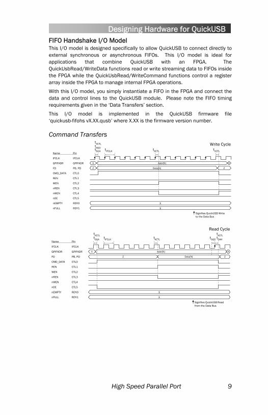
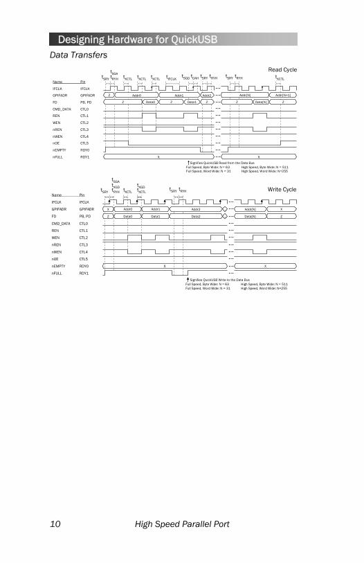
Designing Hardware for QuickUSB FIFO Handshake I/O Model This I/O model is designed specifically to allow QuickUSB to connect directly to external synchronous or asynchronous FIFOs. This I/O model is ideal for applications that combine QuickUSB with an FPGA. The QuickUsbRead/WriteData functions read or write streaming data to FIFOs inside the FPGA while the QuickUsbRead/WriteCommand functions control a register array inside the FPGA to manage internal FPGA operations.
With this I/O model, you simply instantiate a FIFO in the FPGA and connect the data and control lines to the QuickUSB module. Please note the FIFO timing requirements given in the ‘Data Transfers’ section.
This I/O model is implemented in the QuickUSB firmware file ‘quickusb-fifohs vX.XX.qusb’ where X.XX is the firmware version number.
Command Transfers
IFCLK IFCLK
Addr[N]X
tXGD
CMD_DATA CTL0
REN CTL1
WEN CTL2
nREN CTL3
nWEN CTL4
nOE CTL5
GPIFADR GPIFADR
FD PB, PD
Name Pin
Z
Write Cycle
X
Z
nEMPTY RDY0
nFULL RDY1 X
X
tIFCLK tXCTLtSGA
Signifies QuickUSB Write to the Data Bus
tXCTL
tXCTL
Data[N]
IFCLK IFCLK
Addr[N]X
tDAH
CMD_DATA CTL0
REN CTL1
WEN CTL2
nREN CTL3
nWEN CTL4
nOE CTL5
GPIFADR GPIFADR
FD PB, PD
Name Pin
Z Data[N]
Read Cycle
X
Z
nEMPTY RDY0
nFULL RDY1 X
X
tIFCLK tXCTL tSGDtSGA
Signifies QuickUSB Read from the Data Bus
tXCTL tXCTL
High Speed Parallel Port 9
Designing Hardware for QuickUSB Data Transfers
IFCLK IFCLK
Addr0
tDAHtSGD
CMD_DATA CTL0
REN CTL1
WEN CTL2
nREN CTL3
nWEN CTL4
nOE CTL5
GPIFADR GPIFADR
FD PB, PD
Name Pin
Z
Read Cycle
Addr[N]
Z
nEMPTY RDY0
nFULL RDY1 X
tSRY tXCTL
Data0
tRYH
Data1Z Z Data[N]Z
X
tXCTLtSRY tRYHtXCTL tXCTL
tSRY tRYHtIFCLK
Signifies QuickUSB Read from the Data BusFull Speed, Byte Wide: N = 63 High Speed, Byte Wide: N = 511Full Speed, Word Wide: N = 31 High Speed, Word Wide: N=255
Addr1 Addr2 Addr[N+1]Z
tSGA
IFCLK IFCLK
tXGD
CMD_DATA CTL0
REN CTL1
WEN CTL2
nREN CTL3
nWEN CTL4
nOE CTL5
GPIFADR GPIFADR
FD PB, PD
Name PinWrite Cycle
nEMPTY RDY0
nFULL RDY1
X
tSRYtXCTLtRYH
X
tXCTL
Signifies QuickUSB Write to the Data BusFull Speed, Byte Wide: N = 63 High Speed, Byte Wide: N = 511Full Speed, Word Wide: N = 31 High Speed, Word Wide: N=255
tSRY tRYH
tXGD
Addr0
Z Data0
Addr[N]
ZData1 Data2 Data[N]…
Addr1 Addr2 X…X
tSGA
10 High Speed Parallel Port

Designing Hardware for QuickUSB
Full Handshake I/O Model The full handshake I/O model is ideal for connecting a device that has a very slow or variable transfer time. The module checks the state of the READY signal before each state transition and thereby guarantees that the module and target will be properly synchronized at all times.
This I/O model is implemented in the QuickUSB firmware file ‘quickusb-fullhs vX.XX.qusb’ where X.XX is the firmware version number.
Command Transfers
IFCLK IFCLK
X
Data[N] Z
tDAHtSGD
CMD_DATA CTL0
REN CTL1
WEN CTL2
nREN CTL3
nWEN CTL4
RDYTST CTL5
GPIFADR GPIFADR
FD PB, PD
Name Pin
Z Z
X
Data[N]
tXGD
Z
Addr[N]
Read Cycle Write Cycle
READY RDY0
tXCTLtSRY
tXCTL
Addr[N+1] XAddr[N]
tXCTLtRYH
Addr[N+1]X
tSGA tSRY tRYH tXCTLtSRY tRYHtSRYtRYHtSGA
Signifies QuickUSB Read from the Data Bus
Signifies QuickUSB Write to the Data Bus
tXCTLtXCTL
Data Transfers
IFCLK IFCLK
Addr0X
tDAHtSGD
CMD_DATA CTL0
REN CTL1
WEN CTL2
nREN CTL3
nWEN CTL4
RDYTST CTL5
GPIFADR GPIFADR
FD PB, PD
Name Pin
Z Data0
Read Cycle
X
Z
tSGA
READY RDY0
Addr1
Data1
Addr[N]
Data[N]Z Z
tSRY tRYH
… Addr[N+1]
…
tXCTLtXCTL tXCTL tIFCLK tSRY tRYH
Signifies QuickUSB Read from the Data BusFull Speed, Byte Wide: N = 63 High Speed, Byte Wide: N = 511Full Speed, Word Wide: N = 31 High Speed, Word Wide: N=255
IFCLK IFCLK
Addr0X
tXGD
CMD_DATA CTL0
REN CTL1
WEN CTL2
nREN CTL3
nWEN CTL4
RDYTST CTL5
GPIFADR GPIFADR
FD PB, PD
Name Pin
Z Data0
Write Cycle
X
Z
tSGA
READY RDY0
Addr1 Addr[N]
Z Z
tSRY tRYH
Addr[N+1]
tXCTL
tXCTLtIFCLK
Data[N]
tSRY tRYH
Data1
tXGD
tXCTL
…
Signifies QuickUSB Write to the Data BusFull Speed, Byte Wide: N = 63 High Speed, Byte Wide: N = 511Full Speed, Word Wide: N = 31 High Speed, Word Wide: N=255
High Speed Parallel Port 11
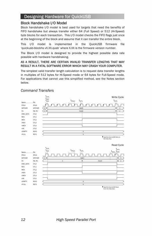
Designing Hardware for QuickUSB Block Handshake I/O Model Block handshake I/O model is best used for targets that need the benefits of FIFO handshake but always transfer either 64 (Full Speed) or 512 (Hi-Speed) byte blocks for each transaction. This I/O model checks the FIFO flags just once at the beginning of the block and assume that it can transfer the entire block.
This I/O model is implemented in the QuickUSB firmware file ‘quickusb-blockhs vX.XX.qusb’ where X.XX is the firmware version number.
The Block I/O model is designed to provide the highest possible data rate possible with hardware handshaking.
AS A RESULT, THERE ARE CERTAIN INVALID TRANSFER LENGTHS THAT MAY RESULT IN A FATAL SOFTWARE ERROR WHICH MAY CRASH YOUR COMPUTER.
The simplest valid transfer length calculation is to request data transfer lengths in multiples of 512 bytes for Hi-Speed mode or 64 bytes for Full-Speed mode. For applications that cannot use this simplified method, see the Notes section below.
Command Transfers
IFCLK IFCLK
Addr0X
tXGD
CMD_DATA CTL0
REN CTL1
WEN CTL2
nREN CTL3
nWEN CTL4
nOE CTL5
GPIFADR GPIFADR
FD PB, PD
Name Pin
Z Data0
Write Cycle
X
Z
nEMPTY RDY0
nFULL RDY1 X
X
tIFCLK tXCTLtSGA
Signifies QuickUSB Write to the Data Bus
tXCTL
tXCTL
IFCLK IFCLK
Addr0X
tDAH
CMD_DATA CTL0
REN CTL1
WEN CTL2
nREN CTL3
nWEN CTL4
nOE CTL5
GPIFADR GPIFADR
FD PB, PD
Name Pin
Z Data0
Read Cycle
X
Z
nEMPTY RDY0
nFULL RDY1 X
X
tIFCLK tXCTL tSGDtSGA
Signifies QuickUSB Read from the Data Bus
tXCTL tXCTL
12 High Speed Parallel Port

Designing Hardware for QuickUSB Data Transfers
nEMPTY RDY0
nFULL RDY1 X X
Signifies QuickUSB Read from the Data BusFull Speed, Byte Wide: N = 63 High Speed, Byte Wide: N = 511Full Speed, Word Wide: N = 31 High Speed, Word Wide: N = 255
tSRY tRYH
IFCLK IFCLK
X
tDAHtSGD
CMD_DATA CTL0
REN CTL1
WEN CTL2
nREN CTL3
nWEN CTL4
nOE CTL5
GPIFADR GPIFADR
FD PB, PD
Name Pin
Z
Read Cycle
Addr1
X Data0
Addr3 Addr4 Addr[N]
Data1 Data2 Data3 Data[N-1] Z
tSGAtIFCLK tXCTL
Data[N]
…
… X
tXCTL
Addr0
tXCTL
…Data4
Addr[N+1]Addr5Addr2 X…
nEMPTY RDY0
nFULL RDY1
X X
Signifies QuickUSB Write to the Data BusFull Speed, Byte Wide: N = 63 High Speed, Byte Wide: N = 511Full Speed, Word Wide: N = 31 High Speed, Word Wide: N = 255
IFCLK IFCLK
Addr0X
tXGD
CMD_DATA CTL0
REN CTL1
WEN CTL2
nREN CTL3
nWEN CTL4
nOE CTL5
GPIFADR GPIFADR
FD PB, PD
Name Pin
Z Data0
Write Cycle
Addr1
Data1
Addr2 Addr3 Addr4 … Addr[N-1] Addr[N] X
Data2 Data3 Data4 Data[N-1] Data[N] Z
tXCTLtIFCLK
Addr[N+1]
…
tXCTL tSGA
Data[N+1]
tSRY tRYH
Notes The valid data transfer length for the Simple I/O model can be calculated with the following pseudo code:
If (DesiredLength MOD PacketSize <= PreRead) Then
ValidLength = PreRead
Else
ValidLength = DesiredLength
Where:
DesiredLength = The desired transfer length
Valid = The valid transfer length
PreRead = 2 for Byte Wide Mode, 4 for Word Wide Mode
PacketSize = 512 for Hi-Speed, 64 for Full-Speed
High Speed Parallel Port 13
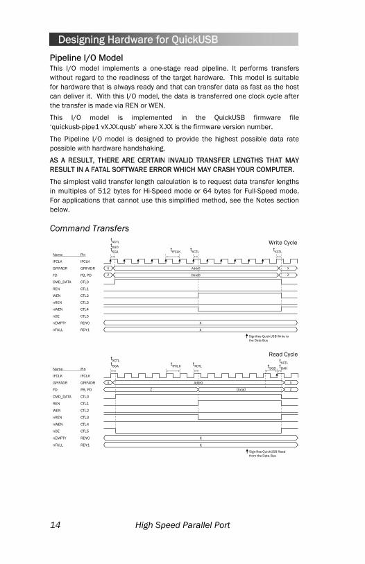
Designing Hardware for QuickUSB Pipeline I/O Model This I/O model implements a one-stage read pipeline. It performs transfers without regard to the readiness of the target hardware. This model is suitable for hardware that is always ready and that can transfer data as fast as the host can deliver it. With this I/O model, the data is transferred one clock cycle after the transfer is made via REN or WEN.
This I/O model is implemented in the QuickUSB firmware file ‘quickusb-pipe1 vX.XX.qusb’ where X.XX is the firmware version number.
The Pipeline I/O model is designed to provide the highest possible data rate possible with hardware handshaking.
AS A RESULT, THERE ARE CERTAIN INVALID TRANSFER LENGTHS THAT MAY RESULT IN A FATAL SOFTWARE ERROR WHICH MAY CRASH YOUR COMPUTER.
The simplest valid transfer length calculation is to request data transfer lengths in multiples of 512 bytes for Hi-Speed mode or 64 bytes for Full-Speed mode. For applications that cannot use this simplified method, see the Notes section below.
Command Transfers
IFCLK IFCLK
Addr0X
tXGD
CMD_DATA CTL0
REN CTL1
WEN CTL2
nREN CTL3
nWEN CTL4
nOE CTL5
GPIFADR GPIFADR
FD PB, PD
Name Pin
Z Data0
Write Cycle
X
Z
nEMPTY RDY0
nFULL RDY1 X
X
tIFCLK tXCTLtSGA
Signifies QuickUSB Write to the Data Bus
tXCTL
tXCTL
IFCLK IFCLK
Addr0X
tDAH
CMD_DATA CTL0
REN CTL1
WEN CTL2
nREN CTL3
nWEN CTL4
nOE CTL5
GPIFADR GPIFADR
FD PB, PD
Name Pin
Z Data0
Read Cycle
X
Z
nEMPTY RDY0
nFULL RDY1 X
X
tIFCLK tXCTL tSGDtSGA
Signifies QuickUSB Read from the Data Bus
tXCTL tXCTL
14 High Speed Parallel Port

Designing Hardware for QuickUSB Data Transfers
IFCLK IFCLK
X
tDAHtSGD
CMD_DATA CTL0
REN CTL1
WEN CTL2
nREN CTL3
nWEN CTL4
nOE CTL5
GPIFADR GPIFADR
FD PB, PD
Name Pin
Z
Read Cycle
Addr1
X Data0
Addr2 Addr3 Addr4 Addr[N-1] Addr[N] X
Data1 Data2 Data3 Data[N-1] Z
tSGA
nEMPTY RDY0
nFULL RDY1 X
X
tIFCLK tXCTL
Addr[N+1]
Data[N]
X
X
…
… X
Signifies QuickUSB Read from the Data BusFull Speed, Byte Wide: N = 63 High Speed, Byte Wide: N = 511Full Speed, Word Wide: N = 31 High Speed, Word Wide: N=255
tXCTL
Addr0
Data[N-2]
tXCTL
…
IFCLK IFCLK
Addr0X
tXGD
CMD_DATA CTL0
REN CTL1
WEN CTL2
nREN CTL3
nWEN CTL4
nOE CTL5
GPIFADR GPIFADR
FD PB, PD
Name Pin
Z Data0
Write Cycle
Addr1
Data1
Addr2 Addr3 Addr4 … Addr[N-1] Addr[N] X
Data2 Data3 Data4 Data[N-1] Data[N] Z
tSGA
nEMPTY RDY0
nFULL RDY1
X
tXCTLtIFCLK
Addr[N+1]
X
X X
…
tXCTL
tXGD tSGA
Signifies QuickUSB Write to the Data BusFull Speed, Byte Wide: N = 63 High Speed, Byte Wide: N = 511Full Speed, Word Wide: N = 31 High Speed, Word Wide: N=255
Data[N+1]
Notes The valid data transfer length for the Simple I/O model can be calculated with the following pseudo code:
If (DesiredLength MOD PacketSize <= PreRead) Then
ValidLength = PreRead
Else
ValidLength = DesiredLength
Where:
DesiredLength = The desired transfer length
Valid = The valid transfer length
PreRead = 2 for Byte Wide Mode, 4 for Word Wide Mode
PacketSize = 512 for Hi-Speed, 64 for Full-Speed
High Speed Parallel Port 15

Designing Hardware for QuickUSB
Slave FIFO I/O Models The HSPP may also be operated in ‘Slave FIFO’ mode. In this mode, the GPIF programmable DMA engine is disabled and the QuickUSB FIFOs are controlled directly by external logic signals. GPIF master mode command/data transfers are not applicable in slave FIFO mode since the GPIF programmable DMA engine is disabled. Slave FIFO mode is selected by changing bits 1-0 of the SETTING_FIFO_CONFIG setting and may be changed at any time. In slave FIFO mode, data is transferred to and from the QuickUSB FIFOs using the standard QuickUsbReadData (EP6) & QuickUsbWriteData (EP2) functions. These endpoints are double-buffered by default. The QuickUSB module can be configured to perform slave FIFO transfers in either synchronously or asynchronously by changing Bit 3 of the SETTING_FIFO_CONFIG setting. The slave FIFO flags may be queried using the SETTING_SLAVEFIFOFLAGS setting.
The following signals are required for slave mode operation:
Pin Name
Alternate Name Description Dir Default Config
IFCLK IFCLK Clock for synchronous I/O In/Out Rising edge FD[15:0] PD[7:0],
PB[7:0] Bi-directional FIFO data bus
Bidir N/A
CTL0 FLAGA Programmable level flag (Half-full)
Out Indexed mode
CTL1 FLAGB FIFO Full Status Flag Out Indexed mode CTL2 FLAGC FIFO Empty Status Flag Out Indexed Mode PA2 nSLOE Enables the FD outputs for
the selected OUT FIFO In Synchronous, Active
low RDY0 nSLRD FIFO read enable/clock In Synchronous, Active
low RDY1 nSLWR FIFO write enable/clock In Synchronous, Active
low PA6 nPKTEND Indicates the end of a short
IN packet In Synchronous, Active
low PA7 nSLCS FIFO Chip Select In Synchronous, Active
low PA5:PA4 FIFOADR[1:0] Selects the active FIFO for
FD and flags. 00=EP2, 01=EP4, 10=EP6, 11=EP8
In N/A
Table 3 - Slave FIFO Mode I/O Connections
There are three Slave FIFO I/O Models available with QuickUSB. For Slave FIFO Modes, no special firmware file is required. Simply use the Simple I/O Model firmware file and program the SETTING_FIFO_CONFIG bit appropriately to implement the desired I/O model.
16 High Speed Parallel Port

Designing Hardware for QuickUSB Synchronous Slave FIFO I/O Model This I/O Model performs all transfers synchronously with IFCLK. This model is configured by setting the SETTING_FIFO_CONFIG bits IFCFG (bits 0-1) to ‘11’ to go to Slave FIFO Mode and ASYNC (bit 3) to ‘0’ to make all transactions synchronous to IFCLK.
IFCLK IFCLK
tXFD
nSLOE PA2
Name Pin
Slave Read Cycle – Data transfer from PC to Slave
tOEon tIFCLK
nSLRD RDY0
nSLWR RDY1
FLAGC (nEMPTY) CTL2
FLAGB (nFULL) CTL1
DATA PB …
tOEofftXFLGtSRD tRDH
FIFOADR[1:0] PA5:PA4
tSFA tFAH
tFAFLG
X
X
tFAFD tSRD
tRDH
tSFAtSRD
tRDH
X
tFAH
tFAFD
tFAFLG
X
X
X ZData0 Data1 Data2 Data3 Data[N-1] Data[N]
00X
Z
X00
nPKTEND PA6
Signifies QuickUSB Write to the Data Bus
nSLCS PA7
IFCLK IFCLK
tXFLG
nSLOE PA2
Name Pin
Z
Slave Write Cycle – Data Transfer from Slave to PC
Z
tSFD tIFCLK
nSLRD RDY0
nSLWR RDY1
FLAGC (nEMPTY) CTL2
FLAGB (nFULL) CTL1
DATA PB Data0 Data[N-1] Data[N]
tFDHtSWR
tWRH
Data[N-2]Data2Data1 Data3 Data4 …
FIFOADR[1:0] PA5:PA4 10X X
tSFA tFAH
tFAFLG
tFAH
X
X
X
X
tFAFLG
nPKTEND PA6
10
tSPE
tPEH
nSLCS PA7
Signifies QuickUSB Read from the Data Bus
Figure 1 - Synchronous Slave FIFO I/O Timing Diagrams
High Speed Parallel Port 17
Designing Hardware for QuickUSB Internally
Sourced IFCLK Externally
Sourced IFCLK Parameter Description Min Max Min Max
Unit
tIFCLK IFCLK Period 20.83 20.83 200 ns tSRD SLRD to Clock Set-up
Time 18.7 12.7 ns
tRDH Clock to SLRD Hold Time 0 3.7 ns
tOEon SLOE Turn-on to FIFO Data Valid 10.5 10.5 ns
tOEoff SLOE Turn-off to FIFO Data Hold 10.5 10.5 ns
tXFLG Clock to FLAGS Output Propagation Delay 9.5 13.5 ns
tXFD Clock to FIFO Data Output Propagation Delay
11 15 ns
tSWR SLWR to Clock Set-up Time 18.1 12.1 ns
tWRH Clock to SLWR Hold Time 0 3.6 ns
tSFD FIFO Data to Clock Set-up Time 9.2 3.2 ns
tFDH Clock to FIFO Data Hold Time 0 4.5 ns
tSFA FIFOADR and nSLCS to Clock Set-up Time 25 ns
tFAH Clock to FIFOADR and nSLCS Hold Time 10 ns
tFAFLG FIFOADR to FLAGS Output Propagation Delay
10.7 ns
tFAFD FIFOADR to FIFO Data Bus Propagation Delay 14.3 ns
tSPE PKTEND to Clock Set-up Time 14.6 8.6 ns
tPEH Clock to PKTEND Hold Time 0 2.5 ns
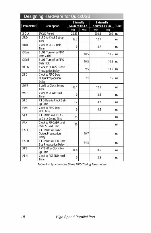
Table 4 – Synchronous Slave FIFO Timing Parameters
18 High Speed Parallel Port

Designing Hardware for QuickUSB
Asynchronous Slave FIFO I/O Model This I/O Model performs all transfers asynchronously using only the rising/falling edge of the nSLRD or nSLWR line to perform the transfer. This model is configured by setting the SETTING_FIFO_CONFIG bits IFCFG (bits 0-1) to ‘11’ to go to Slave FIFO Mode and ASYNC (bit 3) to ‘1’ to make all transactions asynchronous.
tWRpwl
nSLRD RDY0
nSLWR RDY1
FLAGC (nEMPTY) CTL2
FLAGB (nFULL) CTL1
DATA PB
Name PIN
Z
Write Cycle
Data0
tSFDtWRpwh tFDH
Z Data1 Z Data2
tXFDWR
FIFOADR[1:0] PA5:PA4 10X
tSFA
tFAH
nSLOE PA2
tFAH
nPKTEND PA6
tPEpwl tPEpwh
Z
X
tXFLG
Signifies QuickUSB Read from the Data Bus
nSLCS PA7
tRDpwl
Z
Read Cycle
Data0
tXFDRDtRDpwh
Data1 Data2
tXFLG
nSLRD RDY0
nSLWR RDY1
FLAGC (nEMPTY) CTL2
FLAGB (nFULL) CTL1
DATA PB
Name PIN
Z
nSLOE PA2
FIFOADR[1:0] PA5:PA4 00X X
tSFA
tFAHtFAH
tOEon tOEofftXFD
tXFLG
X
X
X
nPKTEND PA6
Signifies QuickUSB Write to the Data Bus
nSLCS PA7
Figure 2 - Asynchronous Slave FIFO I/O Model Timing Diagrams
High Speed Parallel Port 19

Designing Hardware for QuickUSB Parameter Description Min Max Unit
tRDpwl SLRD Pulse Width Low 50 ns tRDpwh SLRD Pulse Width High 50 ns tWRpwl SLWR Pulse Width Low 50 ns tWRpwh SLWR Pulse Width High 70 ns tSFD SLWR to FIFO DATA Set-up Time 10 ns tFDH FIFO DATA to SLWR Hold Time 10 ns tXFLG SLRD to Flags Output Propagation Delay 70 ns tXFDWR SLWR to Flags Output Propagation Delay 70 ns tXFDRD SLRD to FIFO Data Output Propagation Delay 15 ns tOEon SLOE On to FIFO Data Valid 10.5 ns tOEoff SLOE Off to FIFO Data Hold 10.5 ns tSFA FIFOADR/nSLCS to SLRD/SLWR/PKTEND
Set-up Time 10 ns
tFAH SLRD/SLWR/PKTEND to FIFOADR/nSLCS Hold Time 10 ns
tPEpwl PKTEND Pulse Width Low 50 ns tPEpwh PKTEND Pulse Width High 50 ns tXFL PKTEND to Flags Output Propagation Delay 115 ns
Table 5 – Asynchronous Slave FIFO Timing Parameters
20 High Speed Parallel Port

Designing Hardware for QuickUSB Slave245 I/O Model The Slave245 I/O Model allows QuickUSB to duplicate the functionality of the FTDI245BM I/O waveforms with a speed increase of up to 10X. This I/O model is implemented in the QuickUSB firmware file ‘quickusb-245 vX.XX.qusb’ where X.XX is the firmware version number. The following QuickUSB I/O connections are used for 245BM targets:
QuickUSB Signal 245BM Signal RDY0 (nSLRD) and PA2 (SLOE) RD# RDY1 (nSLWR) and PA5 (FIFOADR1) WR CTL2 (FLAGC) RXF# CTL1 (FLAGB ) TXE# PB[7:0] D[7:0] PA4 GND
Figure 3 - QuickUSB to 245BM Connection Table
X
tRDpwlRead Cycle
Data0
tXFDRDtRDpwh
Data1 Data2
tXFLG
RD/SLOE RDY0/PA2
WR/FIFOADR[1] RDY1/PA5
TXE CTL2
RXF CTL1
FD[7:0] PB[7:0]
Name PIN
X
X
Signifies QuickUSB Write to the Data Bus
tXFDRD
X X
tADRFLG
X
tWRpwl
RD/SLOE RDY0/PA2
WR/FIFOADR[1] RDY1/PA5
TXE CTL2
RXF CTL1
FD[7:0] PB[7:0]
Name PIN
Z
Write Cycle
Data0
tSFDtWRpwh tFDH
Z Data1 Z Data2
tXFLG
Z
Signifies QuickUSB Read from the Data Bus
X
Figure 4 - Slave245 I/O Model Timing Diagrams
Parameter Description Min Max Unit tRDpwl SLRD Pulse Width Low 50 ns tRDpwh SLRD Pulse Width High 50 ns tWRpwl SLWR Pulse Width Low 50 ns tWRpwh SLWR Pulse Width High 70 ns tSFD SLWR to FIFO DATA Set-up Time 10 ns tFDH FIFO DATA to SLWR Hold Time 10 ns tXFLG SLRD/SLWR to Flags Output Propagation Delay 70 ns tADRFLG SLWR/FIFOADR[1] to Flags Output Propagation
Delay 10.7 ns
tXFDRD SLRD to FIFO Data Output Propagation Delay 15 ns Figure 5 - Slave245 I/O Model Timing Parameters
High Speed Parallel Port 21

Designing Hardware for QuickUSB
FPGA Configuration The QuickUSB Plug-In module can configure SRAM-based FPGA devices over the USB. The configuration method that QuickUSB uses is based on the SETTING_FPGATYPE setting of the ‘Settings’ section of this document. Currently, two configuration schemes are supported: Altera Passive Serial and Xilinx Slave Serial.
The QuickUSB module uses 3.3V I/O, so make sure your device can handle 3.3V on the configuration pins. Then, connect the FPGA as shown in Table 6. You must be sure to add pull-up resistors required by the FPGA manufacturer. Refer to the FPGA manufacturer’s documentation for the proper configuration connection pin out, signal level and device configuration mode. QuickUSB can transfer an unlimited number of configuration data blocks, so multiple daisy chained devices can be configured using QuickUSB.
QuickUSB Signal Altera PS Xilinx Slave Serial DATA0 DATA0 DIN DCLK DCLK CCLK nCONFIG nCONFIG PROG_B nSTATUS nSTATUS INIT_B CONF_DONE CONF_DONE DONE
Table 6 - FPGA Configuration Signals
General-Purpose I/O Pins The QuickUSB Module implements General Purpose I/O Pins on Ports A, B, C, D, and E when not using the alternate functions for those ports. Please see the ‘QuickUSB Pin Definitions’ section of this user guide for information on the ports and which are being used for alternate functions.
RS-232 The QuickUSB Module’s RS-232 Ports provide standard asynchronous, full-duplex communications. The RS-232 ports operate with no parity, eight data bits, and one stop bit (N81). RS-232 data is received using interrupt-driven receive routines in the module. Both ports operate at the same baud rate.
I2C The QuickUSB I2C-compatible port is a master-only bus controller that can operate in Standard Mode (100kHz) or Fast Mode (400kHz) with 7-bit addressing. The bus speed is selectable using Bit 0 of SETTING_I2CTL. Address 81 (decimal) is reserved. The R/W bit is automatically inserted, so it does not need to be included in the address. The address is automatically shifted to accommodate the R/W bit.
22 FPGA Configuration
Designing Hardware for QuickUSB
SPI The QuickUSB module implements a ‘soft’ SPI port using pins on port E and optionally port A. These routines support from 1 to 10 devices with individual slave select lines for each device. The slave select lines are active low and are shown in Table 7 - QuickUSB Pin Definitions. The signals are MOSI, SCK, MISO and nSS0-9. By default, data is shifted in and out MSbit to LSbit. The bit shift order can be configured by changing Bit 0 of the SETTINGS_SPICONFIG setting. The SPI bus runs at approximately 500Kbps.
SCLK PE1
Name Pin Read Cycle
nSS[9:0] PE[7:6], PA[7:0]
MOSI PE0
MISO PE5
XX
D[N].7X XD[N].6 D[0].2 D[0].1 D[0].0D[N].5 D[N].4 D[N].3 D[N].2 D[N].1
Signifies QuickUSB Read from MISO
SCLK PE1
Name Pin Write Cycle
nSS[9:0] PA[7:0], PE[7:6]
MOSI PE0
MISO PE5 XX
D[N].7X X
Signifies QuickUSB Write to MOSI
D[N].6 D[0].2 D[0].1 D[0].0D[N].5 D[N].4 D[N].3 D[N].2 D[N].1 …
SCLK PE1
Name Pin Write-Read Cycle
nSS[9:0] PA[7:0], PE[7:6]
MOSI PE0
MISO PE5
Dout[N].7X X
Signifies QuickUSB Read from MISO
Dout[N].6 Dout[0].2 Dout[0].1 Dout[0].0Dout[N].5 Dout[N].4 Dout[N].3 Dout[N].2 Dout[N].1
Din[N].7X XDin[N].6 Din[0].2 Din[0].1 Din[0].0Din[N].5 Din[N].4 Din[N].3 Din[N].2 Din[N].1
Signifies QuickUSB Write to MOSI
…
…
Figure 6 - SPI Timing Diagrams
If using any of the slave select signals on Port A (nSS2-9), Port A will convert to the alternate slave select functionality for the entire port. Please ensure you do not use Port A for General Purpose I/O if using the slave select 2-9 (nSS2-9) signals.
If using any of the slave select signals on Port E (nSS0-1) PE6 and PE7 will convert to the alternate slave select functionality for the entire port. Please ensure you do not use PE6 or PE7 for General Purpose I/O if using the nSS0-nSS1 signals.
SPI 23

Designing Hardware for QuickUSB
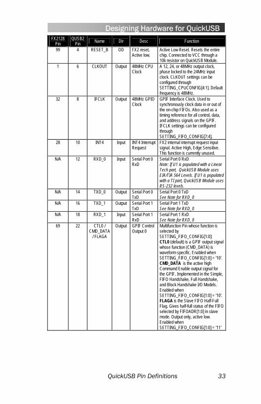
QuickUSB Pin Definitions FX2128
Pin QUSB2
Pin Name Dir Desc Function
N/A 76 SW_EN Output VBUS Switch Enable
SW_EN is high when the QuickUSB Module has successfully enumerated and power can be drawn from VBUS. Used to control the VBUS switch on the QuickUSB Module.
82 3 PA0 / nSS2 / nINT0
I/O Port A, Bit 0 Multifunction Pin PA0 (default) is a bi-directional general purpose I/O pin. nSS2 is the SPI slave select signal for Address 2. Automatically switches functionality when using the SPI commands. Note: If using nSS2-nSS9, all of Port A is converted to slave select functionality, so ensure that Port A is not used for GPIO if using nSS2-nSS9. nINT0 is an active low interrupt input signal. This function is currently unused.
83 5 PA1 / nSS3 / nINT1
I/O Port A, Bit 1 Multifunction Pin PA1 (default) is a bi-directional general purpose I/O pin. nSS3 is the SPI slave select signal for Address 3. Automatically switches functionality when using the SPI commands. See Note for nSS2. nINT1 is an active low interrupt input signal. This function is currently unused.
84 7 PA2 / nSS4 / nSLOE
I/O Port A, Bit 2 Multifunction Pin whose function is selected by SETTING_FIFO_CONFIG[1:0]: PA2 (default) is a bi-directional general purpose I/O pin. Enabled when SETTING_FIFO_CONFIG[1:0]: = '00' or '10' nSS4 is the SPI slave select signal for Address 4. See Note for nSS2. nSLOE is an input-only active low output enable when operating in slave mode. Enabled when
85 9 PA3 / nSS5
I/O Port A, Bit 3 Multifunction Pin PA3 (default) is a bi-directional general purpose I/O pin. nSS5 is the SPI slave select signal for Address 5. See Note for nSS2.
24 QuickUSB Pin Definitions

Designing Hardware for QuickUSB FX2128
Pin QUSB2
Pin Name Dir Desc Function
89 11 PA4 / nSS6/ FIFOADR0
I/O Port A, Bit 4 Multifunction Pin whose function is selected by SETTING_FIFO_CONFIG[1:0]: PA4 (default) is a bi-directional general purpose I/O pin. Enabled when SETTING_FIFO_CONFIG[1:0]: = '00' or '10' nSS6 is the SPI slave select signal for Address 6. See Note for nSS2. FIFOADR0 is an input-only address select for slave devices when operating in slave mode. Enabled when SETTING_FIFO_CONFIG[1:0]: = '11'. See Note for SLOE.
90 13 PA5 / nSS7/ FIFOADR1
I/O Port A, Bit 5 Multifunction Pin whose function is selected by SETTING_FIFO_CONFIG[1:0]: PA5 (default) is a bi-directional general purpose I/O pin. Enabled when SETTING_FIFO_CONFIG[1:0]: = '00' or '10' nSS7 is the SPI slave select signal for Address 7. See Note for nSS2. FIFOADR1 is an input-only address select for slave devices when operating in slave mode. Enabled when SETTING_FIFO_CONFIG[1:0]: = '11'. See Note for SLOE.
91 15 PA6 / nSS8 / nPKTEND
I/O Port A, Bit 6 Multifunction Pin whose function is selected by SETTING_FIFO_CONFIG[1:0]: PA6 (default) is a bi-directional general purpose I/O pin. Enabled when SETTING_FIFO_CONFIG[1:0] ='00' or '10' nSS8 is the SPI slave select signal for Address 8. See Note for nSS2. nPKTEND is an input-only active low signal used to commit the FIFO packet data for slave devices when operating in slave mode. Enabled when SETTING_FIFO_CONFIG[1:0] ='11'. See Note for SLOE.
QuickUSB Pin Definitions 25
Designing Hardware for QuickUSB FX2128
Pin QUSB2
Pin Name Dir Desc Function
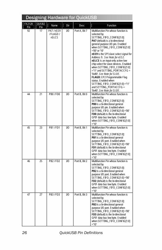
92 17 PA7 / nSS9 / FLAGD /
nSLCS
I/O Port A, Bit 7 Multifunction Pin whose function is selected by SETTING_FIFO_CONFIG[1:0]: PA7 (default) is a bi-directional general purpose I/O pin. Enabled when SETTING_FIFO_CONFIG[1:0] ='00' or '10' nSS9 is the SPI slave select signal for Address 9. See Note for nSS2. nSLCS is an input-only active low chip select for slave devices. Enabled when SETTING_FIFO_CONFIG[1:0] ='11' and SETTING_PORTACCFG = ‘0x80’. See Note for SLOE. FLAGD: EP2 Programmable Flag status. Enabled when SETTING_FIFO_CONFIG[1:0] ='11' and SETTING_PORTACCFG = ‘0x40’. See Note for SLOE.
44 21 PB0 / FD0 I/O Port B, Bit 0 Multifunction Pin whose function is selected by SETTING_FIFO_CONFIG[1:0]: PB0 is a bi-directional general purpose I/O pin. Enabled when SETTING_FIFO_CONFIG[1:0] ='00' FD0 (default) is the bi-directional GPIF data bus low byte. Enabled when SETTING_FIFO_CONFIG[1:0] ='10'
45 23 PB1 / FD1 I/O Port B, Bit 1 Multifunction Pin whose function is selected by SETTING_FIFO_CONFIG[1:0]: PB1 is a bi-directional general purpose I/O port. Enabled when SETTING_FIFO_CONFIG[1:0] ='00' FD1 (default) is the bi-directional GPIF data bus low byte. Enabled when SETTING_FIFO_CONFIG[1:0] ='10'
46 25 PB2 / FD2 I/O Port B, Bit 2 Multifunction Pin whose function is selected by SETTING_FIFO_CONFIG[1:0]: PB2 is a bi-directional general purpose I/O port. Enabled when SETTING_FIFO_CONFIG[1:0] ='00' FD2 (default) is the bi-directional GPIF data bus low byte. Enabled when SETTING_FIFO_CONFIG[1:0] ='10'
47 27 PB3 / FD3 I/O Port B, Bit 3 Multifunction Pin whose function is selected by SETTING_FIFO_CONFIG[1:0]: PB3 is a bi-directional general purpose I/O port. Enabled when SETTING_FIFO_CONFIG[1:0] ='00' FD3 (default) is the bi-directional GPIF data bus low byte. Enabled when SETTING_FIFO_CONFIG[1:0] ='10'
26 QuickUSB Pin Definitions

Designing Hardware for QuickUSB FX2128
Pin QUSB2
Pin Name Dir Desc Function
54 29 PB4 / FD4 I/O Port B, Bit 4 Multifunction Pin whose function is selected by SETTING_FIFO_CONFIG[1:0]: PB4 is a bi-directional general purpose I/O port. Enabled when SETTING_FIFO_CONFIG[1:0] ='00' FD4 (default) is the bi-directional GPIF data bus low byte. Enabled when SETTING_FIFO_CONFIG[1:0] ='10'
55 31 PB5 / FD5 I/O Port B, Bit 5 Multifunction Pin whose function is selected by SETTING_FIFO_CONFIG[1:0]: PB5 is a bi-directional general purpose I/O port. Enabled when SETTING_FIFO_CONFIG[1:0] ='00' FD5 (default) is the bi-directional GPIF data bus low byte. Enabled when SETTING_FIFO_CONFIG[1:0] ='10'
56 33 PB6 / FD6 I/O Port B, Bit 6 Multifunction Pin whose function is selected by SETTING_FIFO_CONFIG[1:0]: PB6 is a bi-directional general purpose I/O port. Enabled when SETTING_FIFO_CONFIG[1:0] ='00' FD6 (default) is the bi-directional GPIF data bus low byte. Enabled when SETTING_FIFO_CONFIG[1:0] ='10'
57 35 PB7 / FD7 I/O Port B, Bit 7 Multifunction Pin whose function is selected by SETTING_FIFO_CONFIG[1:0]: PB7 is a bi-directional general purpose I/O port. Enabled when SETTING_FIFO_CONFIG[1:0] ='00' FD7 (default) is the bi-directional GPIF data bus low byte. Enabled when SETTING_FIFO_CONFIG[1:0] ='10'
72 39 PC0 / GPIFADR0
I/O Port C, Bit 0 Multifunction Pin whose function is selected by SETTING_FIFO_CONFIG[1:0]: PC0 is a bi-directional general purpose I/O port. Enabled when SETTING_FIFO_CONFIG[1:0] ='00' GPIFADR0 (default) is a GPIF address output pin. Enabled when SETTING_FIFO_CONFIG[1:0] ='10'
73 41 PC1 / GPIFADR1
I/O Port C, Bit 1 Multifunction Pin whose function is selected by SETTING_FIFO_CONFIG[1:0]: PC1 is a bi-directional general purpose I/O port. Enabled when SETTING_FIFO_CONFIG[1:0] ='00' GPIFADR1 (default) is a GPIF address output pin. Enabled when SETTING_FIFO_CONFIG[1:0] ='10'
QuickUSB Pin Definitions 27

Designing Hardware for QuickUSB FX2128
Pin QUSB2
Pin Name Dir Desc Function
74 43 PC2 / GPIFADR2
I/O Port C, Bit 2 Multifunction Pin whose function is selected by SETTING_FIFO_CONFIG[1:0]: PC2 is a bi-directional general purpose I/O port. Enabled when SETTING_FIFO_CONFIG[1:0] ='00' GPIFADR2 (default) is a GPIF address output pin. Enabled when SETTING_FIFO_CONFIG[1:0] ='10'
75 45 PC3 / GPIFADR3
I/O Port C, Bit 3 Multifunction Pin whose function is selected by SETTING_FIFO_CONFIG[1:0]: PC3 is a bi-directional general purpose I/O port. Enabled when SETTING_FIFO_CONFIG[1:0] ='00' GPIFADR3 (default) is a GPIF address output pin. Enabled when SETTING_FIFO_CONFIG[1:0] ='10'
76 47 PC4 / GPIFADR4
I/O Port C, Bit 4 Multifunction Pin whose function is selected by SETTING_FIFO_CONFIG[1:0]: PC4 is a bi-directional general purpose I/O port. Enabled when SETTING_FIFO_CONFIG[1:0] ='00' GPIFADR4 (default) is a GPIF address output pin. Enabled when SETTING_FIFO_CONFIG[1:0] ='10'
77 49 PC5 / GPIFADR5
I/O Port C, Bit 5 Multifunction Pin whose function is selected by SETTING_FIFO_CONFIG[1:0]: PC5 is a bi-directional general purpose I/O port. Enabled when SETTING_FIFO_CONFIG[1:0] ='00' GPIFADR5 (default) is a GPIF address output pin. Enabled when SETTING_FIFO_CONFIG[1:0] ='10'
78 51 PC6 / GPIFADR6
I/O Port C, Bit 6 Multifunction Pin whose function is selected by SETTING_FIFO_CONFIG[1:0]: PC6 is a bi-directional general purpose I/O port. Enabled when SETTING_FIFO_CONFIG[1:0] ='00' GPIFADR6 (default) is a GPIF address output pin. Enabled when SETTING_FIFO_CONFIG[1:0] ='10'
79 53 PC7 / GPIFADR7
I/O Port C, Bit 7 Multifunction Pin whose function is selected by SETTING_FIFO_CONFIG[1:0]: PC7 is a bi-directional general purpose I/O port. Enabled when SETTING_FIFO_CONFIG[1:0] ='00' GPIFADR7 (default) is a GPIF address output pin. Enabled when SETTING_FIFO_CONFIG[1:0] ='10'
28 QuickUSB Pin Definitions

Designing Hardware for QuickUSB FX2128
Pin QUSB2
Pin Name Dir Desc Function
102 57 PD0 / FD8 I/O Port D, Bit 0 Multifunction Pin whose function is selected by SETTING_FIFO_CONFIG[1:0]: PD0 is a bi-directional general purpose I/O port. Enabled when SETTING_FIFO_CONFIG[1:0] ='00' or when SETTING_WORDWIDE = '0' FD8 (default) is the bi-directional GPIF data bus. Enabled when SETTING_FIFO_CONFIG[1:0] ='10' and when SETTING_WORDWIDE = '1'
103 59 PD1 / FD9 I/O Port D, Bit 1 Multifunction Pin whose function is selected by SETTING_FIFO_CONFIG[1:0]: PD1 is a bi-directional general purpose I/O port. Enabled when SETTING_FIFO_CONFIG[1:0] ='00' or when SETTING_WORDWIDE = '0' FD9 (default) is the bi-directional GPIF data bus. Enabled when SETTING_FIFO_CONFIG[1:0] ='10' and when SETTING_WORDWIDE = '1'
104 61 PD2 / FD10 I/O Port D, Bit 2 Multifunction Pin whose function is selected by SETTING_FIFO_CONFIG[1:0]: PD2 is a bi-directional general purpose I/O port. Enabled when SETTING_FIFO_CONFIG[1:0] ='00' or when SETTING_WORDWIDE = '0' FD10 (default) is the bi-directional GPIF data bus. Enabled when SETTING_FIFO_CONFIG[1:0] ='10' and when SETTING_WORDWIDE = '1'
105 63 PD3 / FD11 I/O Port D, Bit 3 Multifunction Pin whose function is selected by SETTING_FIFO_CONFIG[1:0]: PD3 is a bi-directional general purpose I/O port. Enabled when SETTING_FIFO_CONFIG[1:0] ='00' or when SETTING_WORDWIDE = '0' FD11 (default) is the bi-directional GPIF data bus. Enabled when SETTING_FIFO_CONFIG[1:0] ='10' and when SETTING_WORDWIDE = '1'
QuickUSB Pin Definitions 29

Designing Hardware for QuickUSB FX2128
Pin QUSB2
Pin Name Dir Desc Function
121 65 PD4 / FD12 I/O Port D, Bit 4 Multifunction Pin whose function is selected by SETTING_FIFO_CONFIG[1:0]: PD4 is a bi-directional general purpose I/O port. Enabled when SETTING_FIFO_CONFIG[1:0] ='00' or when SETTING_WORDWIDE = '0' FD12 (default) is the bi-directional GPIF data bus. Enabled when SETTING_FIFO_CONFIG[1:0] ='10' and when SETTING_WORDWIDE = '1'
122 67 PD5 / FD13 I/O Port D, Bit 5 Multifunction Pin whose function is selected by SETTING_FIFO_CONFIG[1:0]: PD5 is a bi-directional general purpose I/O port. Enabled when SETTING_FIFO_CONFIG[1:0] ='00' or when SETTING_WORDWIDE = '0' FD13 is the bi-directional GPIF data bus. Enabled when SETTING_FIFO_CONFIG[1:0] ='10' and when SETTING_WORDWIDE = '1'
123 69 PD6 / FD14 I/O Port D, Bit 6 Multifunction Pin whose function is selected by SETTING_FIFO_CONFIG[1:0]: PD6 is a bi-directional general purpose I/O port. Enabled when SETTING_FIFO_CONFIG[1:0] ='00' or when SETTING_WORDWIDE = '0' FD14 is the bi-directional GPIF data bus. Enabled when SETTING_FIFO_CONFIG[1:0] ='10' and when SETTING_WORDWIDE = '1'
124 71 PD7 / FD15 I/O Port D, Bit 7 Multifunction Pin whose function is selected by SETTING_FIFO_CONFIG[1:0]: PD7 is a bi-directional general purpose I/O port. Enabled when SETTING_FIFO_CONFIG[1:0] ='00' or when SETTING_WORDWIDE = '0' FD15 (default) is the bi-directional GPIF data bus. Enabled when SETTING_FIFO_CONFIG[1:0] ='10' and when SETTING_WORDWIDE = '1'
30 QuickUSB Pin Definitions

Designing Hardware for QuickUSB FX2128
Pin QUSB2
Pin Name Dir Desc Function
108 58 PE0 / DATA0 /
MOSI
I/O Port E, Bit 0 Multifunction Pin PE0 (default) is a bi-directional general purpose I/O port. Enabled when SETTING_FIFO_CONFIG[1:0] ='00', '10', or '11' DATA0 is the data output signal for serial FPGA configuration. Automatically switches functionality when using the FPGA configuration commands. MOSI is the Master-Out Slave-In data signal for the SPI port. Automatically switches functionality when using the SPI commands.
109 60 PE1 / DCLK / SCK
I/O Port E, Bit 1 Multifunction Pin PE1 (default) is a bi-directional general purpose I/O port. Enabled when SETTING_FIFO_CONFIG[1:0] ='00', '10', or '11' DCLK is the clock output signal for serial FPGA configuration. Automatically switches functionality when using the FPGA configuration commands. SCLK is the clock output signal for the SPI port. Automatically switches functionality when using the SPI commands.
110 62 PE2 / nCE I/O Port E, Bit 2 Multifunction Pin PE2 is a bi-directional general purpose I/O port. Enabled when SETTING_FIFO_CONFIG[1:0] ='00', '10', or '11' nCE is available for use as a Chip Enable signal for SPI commands. It is controlled using the normal GPIO function calls.
111 64 PE3 / nCONFIG
I/O Port E, Bit 3 Multifunction Pin PE3 (default) is a bi-directional general purpose I/O port. Enabled when SETTING_FIFO_CONFIG[1:0] ='00', '10', or '11' nCONFIG is the Configure/Program output signal for serial FPGA configuration. Automatically switches functionality when using the FPGA configuration commands.
112 66 PE4 / nSTATUS
I/O Port E, Bit 4 Multifunction Pin PE4 (default) is a bi-directional general purpose I/O port. Enabled when SETTING_FIFO_CONFIG[1:0] ='00', '10', or '11' nSTATUS is the Status input signal for serial FPGA configuration. Automatically switches functionality when using the FPGA configuration commands.
QuickUSB Pin Definitions 31

Designing Hardware for QuickUSB FX2128
Pin QUSB2
Pin Name Dir Desc Function
113 68 PE5 / CONF_DONE / MISO
I/O Port E, Bit 5 Multifunction Pin PE5 (default) is a bi-directional general purpose I/O port. Enabled when SETTING_FIFO_CONFIG[1:0] ='00', '10', or '11' CONF_DONE is the Done output signal for serial FPGA configuration. Automatically switches functionality when using the FPGA configuration commands. MISO is the Master-In Slave-Out data signal for the SPI port. Automatically switches functionality when using the SPI commands.
114 70 PE6 / nSS0 I/O Port E, Bit 6 Multifunction Pin PE6 (default) is a bi-directional general purpose I/O port. Enabled when SETTING_FIFO_CONFIG[1:0] ='00', '10', or '11' nSS0 is the active low slave select signal for Address 0 of the SPI port. Automatically switches functionality when using the SPI commands. Note: If using nSS0-nSS1, PE6 and PE7 convert to SPI slave select functionality, so ensure that PE6 and PE7 are not used for GPIO if using SPI nSS0-nSS1.
115 72 PE7 / GPIFADR8
/ nSS1
I/O Port E, Bit 7 Multifunction Pin PE7 is a bi-directional general purpose I/O port. Enabled when SETTING_FIFO_CONFIG[1:0] ='00', or '11' GPIFADR8 (default) is a GPIF address output pin. Enabled when SETTING_FIFO_CONFIG[1:0] ='10' nSS1 is the active low slave select signal for Address 1 of the SPI port. Automatically switches functionality when using the SPI commands. See Note for nSS0.
36 73 SCL Output Clock for I2C interface
Clock for I2C Interface. Connect to VCC with a 2.2K resistor, even if no I2C peripheral is attached. Connected to VCC with 2.2K resistor on QuickUSB Module.
37 75 SDA OD Data for I2C interface
Data for I2C Interface. Connect to VCC with a 2.2K resistor, even if no I2C peripheral is attached. Connected to VCC with 2.2K resistor on QuickUSB Module.
29 77 T0 Input Input for Timer0
Active High Input to Timer0. Not needed for general operation.
30 78 T1 Input Input for Timer1
Active High input to Timer1. Not needed for general operation.
31 N/A T2 Input Input for Timer2
Active High input to Timer2. Connected to VCC through 2.2k resistor on QuickUSB Module.
32 QuickUSB Pin Definitions
Designing Hardware for QuickUSB FX2128
Pin QUSB2
Pin Name Dir Desc Function
99 4 RESET_B OD FX2 reset, Active low.
Active Low Reset. Resets the entire chip. Connected to VCC through a 10k resistor on QuickUSB Module.
1 6 CLKOUT Output 48MHz CPU Clock
A 12, 24, or 48MHz output clock, phase locked to the 24MHz input clock. CLKOUT settings can be configured through SETTING_CPUCONFIG[4:1]. Default frequency is 48MHz.
32 8 IFCLK Output 48MHz GPIO Clock
GPIF Interface Clock. Used to synchronously clock data in or out of the on-chip FIFOs. Also used as a timing reference for all control, data, and address signals on the GPIF. IFCLK settings can be configured through SETTING_FIFO_CONFIG[7:4].
28 10 INT4 Input INT4 Interrupt Request
FX2 internal interrupt request input signal. Active High, Edge Sensitive. This function is currently unused.
N/A 12 RXD_0 Input Serial Port 0 RxD
Serial Port 0 RxD Note: If U1 is populated with a Linear Tech part, QuickUSB Module uses EIA/TIA 564 Levels. If U1 is populated with a TI part, QuickUSB Module uses RS-232 levels.
N/A 14 TXD_0 Output Serial Port 0 TxD
Serial Port 0 TxD See Note for RXD_0
N/A 16 TXD_1 Output Serial Port 1 TxD
Serial Port 1 TxD See Note for RXD_0
N/A 18 RXD_1 Input Serial Port 1 RxD
Serial Port 1 RxD See Note for RXD_0
69 22 CTL0 / CMD_DATA
/ FLAGA
Output GPIF Control Output 0
Multifunction Pin whose function is selected by SETTING_FIFO_CONFIG[1:0]: CTL0 (default) is a GPIF output signal whose function (CMD_DATA) is waveform specific. Enabled when SETTING_FIFO_CONFIG[1:0] = '10'. CMD_DATA is the active high Command Enable output signal for the GPIF. Implemented in the Simple, FIFO Handshake, Full Handshake, and Block Handshake I/O Models. Enabled when SETTING_FIFO_CONFIG[1:0] = '10'. FLAGA is the Slave FIFO Half-Full Flag. Gives half-full status of the FIFO selected by FIFOADR[1:0] in slave mode. Output only, active low. Enabled when SETTING_FIFO_CONFIG[1:0] = '11'
QuickUSB Pin Definitions 33
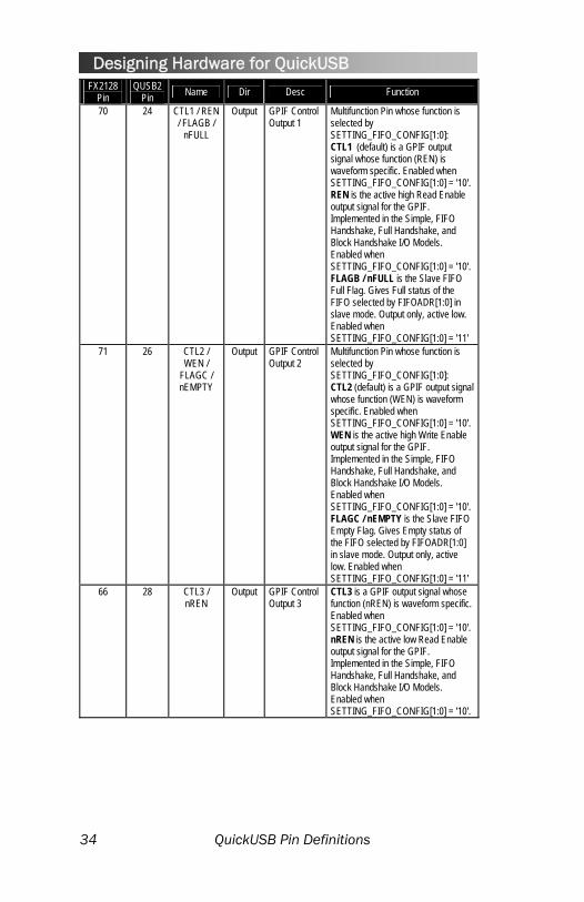
Designing Hardware for QuickUSB FX2128
Pin QUSB2
Pin Name Dir Desc Function
70 24 CTL1 / REN / FLAGB /
nFULL
Output GPIF Control Output 1
Multifunction Pin whose function is selected by SETTING_FIFO_CONFIG[1:0]: CTL1 (default) is a GPIF output signal whose function (REN) is waveform specific. Enabled when SETTING_FIFO_CONFIG[1:0] = '10'. REN is the active high Read Enable output signal for the GPIF. Implemented in the Simple, FIFO Handshake, Full Handshake, and Block Handshake I/O Models. Enabled when SETTING_FIFO_CONFIG[1:0] = '10'. FLAGB / nFULL is the Slave FIFO Full Flag. Gives Full status of the FIFO selected by FIFOADR[1:0] in slave mode. Output only, active low. Enabled when SETTING_FIFO_CONFIG[1:0] = '11'
71 26 CTL2 / WEN /
FLAGC / nEMPTY
Output GPIF Control Output 2
Multifunction Pin whose function is selected by SETTING_FIFO_CONFIG[1:0]: CTL2 (default) is a GPIF output signal whose function (WEN) is waveform specific. Enabled when SETTING_FIFO_CONFIG[1:0] = '10'. WEN is the active high Write Enable output signal for the GPIF. Implemented in the Simple, FIFO Handshake, Full Handshake, and Block Handshake I/O Models. Enabled when SETTING_FIFO_CONFIG[1:0] = '10'. FLAGC / nEMPTY is the Slave FIFO Empty Flag. Gives Empty status of the FIFO selected by FIFOADR[1:0] in slave mode. Output only, active low. Enabled when SETTING_FIFO_CONFIG[1:0] = '11'
66 28 CTL3 / nREN
Output GPIF Control Output 3
CTL3 is a GPIF output signal whose function (nREN) is waveform specific. Enabled when SETTING_FIFO_CONFIG[1:0] = '10'. nREN is the active low Read Enable output signal for the GPIF. Implemented in the Simple, FIFO Handshake, Full Handshake, and Block Handshake I/O Models. Enabled when SETTING_FIFO_CONFIG[1:0] = '10'.
34 QuickUSB Pin Definitions

Designing Hardware for QuickUSB FX2128
Pin QUSB2
Pin Name Dir Desc Function
67 30 CTL4 / nWEN
Output GPIF Control Output 4
CTL4 is a GPIF output signal whose function (nWEN) is waveform specific. Enabled when SETTING_FIFO_CONFIG[1:0] = '10'. nWEN is the active low Write Enable output signal for the GPIF. Implemented in the Simple, FIFO Handshake, Full Handshake, and Block Handshake I/O Models. Enabled when SETTING_FIFO_CONFIG[1:0] = '10'.
98 32 CTL5 / nOE / RDYTST
Output GPIF Control Output 5
CTL5 is a GPIF output signal whose function (nOE or RDYTST) is waveform specific. Enabled when SETTING_FIFO_CONFIG[1:0] = '10'. nOE is the active low Output Enable output signal for the GPIF. Implemented in the Simple, FIFO Handshake, and Block Handshake I/O Models. Enabled when SETTING_FIFO_CONFIG[1:0] = '10'. RDYTST is the Ready Test output signal for the Full Handshake I/O Model. RDYTST outputs the correct handshake waveform for the READY line, so it can be connected to READY to test the Full Handshake functionality. Implemented in the Full Handshake I/O Model. Enabled when SETTING_FIFO_CONFIG[1:0] = '10'.
51 34 RXD0 Input Serial Port 0 TTL RxD
RXD0 is the receive signal for the 8051 UART0. Active High, Input only. Do not use if U1 is populated on the QuickUSB Module.
50 36 TXD0 Output Serial Port 0 TTL RxD
TXD0 is the transmit signal for the 8051 UART0. Active High, Output only. Do not use if U1 is populated on the QuickUSB Module.
53 52 RXD1 Input Serial Port 1 TTL RxD
RXD1 is the receive signal for the 8051 UART1. Active High, Input only. Do not use if U1 is populated on the QuickUSB Module.
52 54 TXD1 Output Serial Port 1 TTL RxD
TXD1 is the transmit signal for the 8051 UART1. Active High, Output only. Do not use if U1 is populated on the QuickUSB Module.
QuickUSB Pin Definitions 35

Designing Hardware for QuickUSB FX2128
Pin QUSB2
Pin Name Dir Desc Function
4 40 RDY0 / nEMPTY / READY / nSLRD
Input GPIF input signal 0
Multifunction Pin whose function is selected by SETTING_FIFO_CONFIG[1:0]: RDY0 (default) is a GPIF input signal whose function (nEMPTY or READY) is waveform specific. Enabled when SETTING_FIFO_CONFIG[1:0] = '10' nEMPTY is an active low input that checks the status of the EMPTY flag of a connected FIFO. Implemented in the FIFO Handshake and Block Handshake I/O Models. Enabled when SETTING_FIFO_CONFIG[1:0] = '10' READY is an input that checks the status of the READY flag of a slave device. Implemented in the Full Handshake I/O Model. Enabled when SETTING_FIFO_CONFIG[1:0] = '10' nSLRD is the Slave Read Strobe. Input only, active low. Enabled when SETTING_FIFO_CONFIG[1:0] = '11'
5 42 RDY1 / nFULL / nSLWR
Input GPIF input signal 1
Multifunction Pin whose function is selected by SETTING_FIFO_CONFIG[1:0]: RDY1 (default) is a GPIF input whose function (nFULL) is waveform specific. Enabled when SETTING_FIFO_CONFIG[1:0] = '10' nFULL is an active low input that checks the status of the FULL flag of a connected FIFO. Implemented in the FIFO Handshake and Block Handshake waveforms. Enabled when SETTING_FIFO_CONFIG[1:0] = '10' nSLWR is the Slave Write Strobe. Input only, active low. Enabled when SETTING_FIFO_CONFIG[1:0] = '11'
6 44 RDY2 Input GPIF input signal 2
RDY2 is a GPIF input signal. Enabled when SETTING_FIFO_CONFIG[1:0] = '10'. Not currently used by QuickUSB.
7 46 RDY3 Input GPIF input signal 3
RDY3 is a GPIF input signal. Enabled when SETTING_FIFO_CONFIG[1:0] = '10'. Not currently used by QuickUSB.
8 48 RDY4 Input GPIF input signal 4
RDY4 is a GPIF input signal. Enabled when SETTING_FIFO_CONFIG[1:0] = '10'. Not currently used by QuickUSB.
9 50 RDY5 Input GPIF input signal 5
RDY5 is a GPIF input signal. Enabled when SETTING_FIFO_CONFIG[1:0] = '10'. Not currently used by QuickUSB.
36 QuickUSB Pin Definitions

Designing Hardware for QuickUSB FX2128
Pin QUSB2
Pin Name Dir Desc Function
101 74 WAKEUP_B
Input USB Wakeup USB Wakeup. Asserting pin brings FX2 out of suspend mode. Active Low. Not used, connected to VCC through a 10k resistor on QuickUSB Module.
19 N/A DMINUS I/O USB D- Signal
Connect to the USB D- Signal
18 N/A DPLUS I/O USB D+ Signal
Connect to the USB D+ Signal
94 N/A A0 Output 95 N/A A1 Output 96 N/A A2 Output 97 N/A A3 Output
117 N/A A4 Output 118 N/A A5 Output 119 N/A A6 Output 120 N/A A7 Output 126 N/A A8 Output 127 N/A A9 Output 128 N/A A10 Output 21 N/A A11 Output 22 N/A A12 Output 23 N/A A13 Output 24 N/A A14 Output 25 N/A A15 Output
8051 Address Bus
8051 Address Bus. Driven at all times. Reflects internal address when 8051 is addressing RAM. Not connected on QuickUSB Module.
59 N/A D0 I/O 60 N/A D1 I/O 61 N/A D2 I/O 62 N/A D3 I/O 63 N/A D4 I/O 86 N/A D5 I/O 87 N/A D6 I/O 88 N/A D7 I/O
8051 Data Bus
8051 Data Bus. Bi-directional bus used for external 8051 program and data memory. High Impedance when inactive. Active only for external bus accesses. Driven low in suspend. Not connected on QuickUSB Module.
39 N/A PSEN# Output Program Store Enable
Indicates an 8051 code fetch from external memory. Active low.
34 N/A BKPT Output Breakpoint Used as SW_EN on the QuickUSB module to control the onboard VBUS switch.
35 N/A EA Input External Access
Determines where the 8051 fetches code from RAM. If EA=0, 8051 fetches from internal Ram. If EA=1, 8051 fetches from external RAM. Tied to GND through 10k Resistor on QuickUSB Module.
12 N/A XTALIN Input Crystal Input Connect to 24MHz parallel resonant, fundamental mode crystal and connect the parallel load capacitor to GND.
11 N/A XTALOUT Output Crystal Output
Connect to 24MHz parallel resonant, fundamental mode crystal and connect the parallel load capacitor to GND.
42 N/A CS# Output External Memory Chip Select
External Memory Chip Select. Active Low. Not connected on QuickUSB Module
QuickUSB Pin Definitions 37
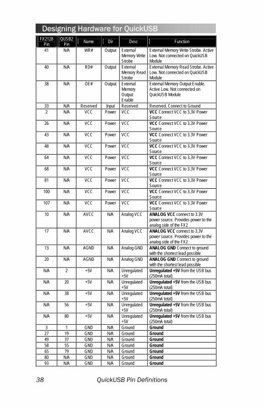
Designing Hardware for QuickUSB FX2128
Pin QUSB2
Pin Name Dir Desc Function
41 N/A WR# Output External Memory Write Strobe
External Memory Write Strobe. Active Low. Not connected on QuickUSB Module
40 N/A RD# Output External Memory Read Strobe
External Memory Read Strobe. Active Low. Not connected on QuickUSB Module
38 N/A OE# Output External Memory Output Enable
External Memory Output Enable. Active Low. Not connected on QuickUSB Module
33 N/A Reserved Input Reserved Reserved. Connect to Ground 2 N/A VCC Power VCC VCC Connect VCC to 3.3V Power
Source 26 N/A VCC Power VCC VCC Connect VCC to 3.3V Power
Source 43 N/A VCC Power VCC VCC Connect VCC to 3.3V Power
Source 48 N/A VCC Power VCC VCC Connect VCC to 3.3V Power
Source 64 N/A VCC Power VCC VCC Connect VCC to 3.3V Power
Source 68 N/A VCC Power VCC VCC Connect VCC to 3.3V Power
Source 81 N/A VCC Power VCC VCC Connect VCC to 3.3V Power
Source 100 N/A VCC Power VCC VCC Connect VCC to 3.3V Power
Source 107 N/A VCC Power VCC VCC Connect VCC to 3.3V Power
Source 10 N/A AVCC N/A Analog VCC ANALOG VCC connect to 3.3V
power source. Provides power to the analog side of the FX2
17 N/A AVCC N/A Analog VCC ANALOG VCC connect to 3.3V power source. Provides power to the analog side of the FX2
13 N/A AGND N/A Analog GND ANALOG GND Connect to ground with the shortest lead possible
20 N/A AGND N/A Analog GND ANALOG GND Connect to ground with the shortest lead possible
N/A 2 +5V N/A Unregulated +5V
Unregulated +5V from the USB bus (250mA total)
N/A 20 +5V N/A Unregulated +5V
Unregulated +5V from the USB bus (250mA total)
N/A 38 +5V N/A Unregulated +5V
Unregulated +5V from the USB bus (250mA total)
N/A 56 +5V N/A Unregulated +5V
Unregulated +5V from the USB bus (250mA total)
N/A 80 +5V N/A Unregulated +5V
Unregulated +5V from the USB bus (250mA total)
3 1 GND N/A Ground Ground 27 19 GND N/A Ground Ground 49 37 GND N/A Ground Ground 58 55 GND N/A Ground Ground 65 79 GND N/A Ground Ground 80 N/A GND N/A Ground Ground 93 N/A GND N/A Ground Ground
38 QuickUSB Pin Definitions
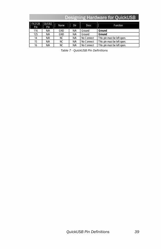
Designing Hardware for QuickUSB FX2128
Pin QUSB2
Pin Name Dir Desc Function
116 N/A GND N/A Ground Ground 125 N/A GND N/A Ground Ground 14 N/A NC N/A No Connect This pin must be left open. 15 N/A NC N/A No Connect This pin must be left open. 16 N/A NC N/A No Connect This pin must be left open.
Table 7 - QuickUSB Pin Definitions
QuickUSB Pin Definitions 39

Using the QuickUSB Library
Using the QuickUSB Library
Overview The QuickUSB® Library API gives programmers a cohesive programming interface to the QuickUSB family of products. The same QuickUSB Library API works for all QuickUSB products on all platforms, so you write your software once and all your QuickUSB based products will work on any supported platform.
The QuickUSB library offers support for many programming languages. The QuickUSB Library includes support for the following programming languages:
• Microsoft Visual Basic 6.0 • Microsoft C/C++ version 6.0, MFC dialog and command line • Microsoft .NET 2003 • Borland C++ Builder 5.0 • Borland Delphi 4.0 • LabView 7.0 • Qt Designer
This API documentation is language independent. To find the particular parameter type, please consult the QuickUSB Library include files for your programming language.
There are three basic methods of interfacing with the QuickUSB Library, using a function-based API, a class-based API or a using a QuickUSB component.
The function-based API makes calls to the QuickUSB Library directly from your programming language. For instance, your application will include a file that has all the QuickUSB function declarations then from your code, you would call the appropriate functions to implement the behavior you need.
The class-based API makes the QuickUSB Library level calls from an object-oriented interface. Your code instantiates one or more CQuickUSB objects and calls the methods to implement the required behavior.
The component-based approach displays available modules and lets the user interact with the component GUI to make that selection, and then the app calls component methods to implement the required behavior.
How to Communicate with a Module The general procedure to use a QuickUSB module is given below:
1. Call QuickUsbFindModules to get a list of available modules. The list will be returned as a NULL-delimited string.
2. Parse the list of available modules and provide a means to select the desired module.
3. Then, for each data transaction (send or receive): a. Call QuickUsbOpen and pass in the device name. A new device id is
returned on success. b. Call the data transfer functions needed by your application. c. Call QuickUsbClose to close the handle to the USB module.
40 Overview
Using the QuickUSB Library
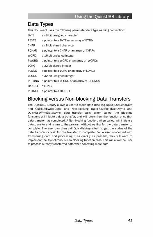
Data Types This document uses the following parameter data type naming convention:
BYTE an 8-bit unsigned character
PBYTE a pointer to a BYTE or an array of BYTEs
CHAR an 8-bit signed character
PCHAR a pointer to a CHAR or an array of CHARs
WORD a 16-bit unsigned integer
PWORD a pointer to a WORD or an array of WORDs
LONG a 32-bit signed integer
PLONG a pointer to a LONG or an array of LONGs
ULONG a 32-bit unsigned integer
PULONG a pointer to a ULONG or an array of ULONGs
HANDLE a LONG
PHANDLE a pointer to a HANDLE
Blocking versus Non-blocking Data Transfers The QuickUSB Library allows a user to make both Blocking (QuickUsbReadData and QuickUsbWriteData) and Non-blocking (QuickUsbReadDataAsync and QuickUsbWriteDataAsync) data transfer calls. When called, the Blocking functions will initiate a data transfer, and will return from the function once that data transfer has completed. A Non-blocking function, when called, will initiate a data transfer and return to the program without waiting for the data transfer to complete. The user can then call QuickUsbAsyncWait to get the status of the data transfer or wait for the transfer to complete. For a user concerned with transferring data and processing it as quickly as possible, they will want to implement the Asynchronous Non-blocking function calls. This will allow the user to process already transferred data while collecting more data.
Data Types 41

Using the QuickUSB Library QuickUSB Base API General purpose functions to manage the operation of the QuickUSB module and the Library.
QuickUsbFindModules Purpose
Build a list of all QuickUSB modules connected to the host.
Parameters nameList: A PCHAR that points to a buffer in which to store a of
QuickUSB module names found by the library. Device names are of the form ‘QUSB-XXX’ where XXX is the device address (0-126) in decimal. ‘nameList’ must be large enough to contain all the device names + 1 character.
length: A LONG containing the length of the nameList buffer in CHARs.
Returns A LONG that is either non-zero on success or zero (0) on failure. If successful, nameList will contain a NULL (‘\0’ or CHR(0)) delimited list of QuickUSB module names found by the library. The final entry is designated by two consecutive NULL characters. For example, after executing this function with one module connected, nameList will contain "QUSB-0\0\0". If there are two devices plugged in, nameList will contain "QUSB-0\0QUSB-1\0\0".
Notes This routine will only find devices that are closed.
QuickUsbOpen Purpose
Open a QuickUSB device for use by the library
Parameters hDevice: A PHANDLE that points to a HANDLE in which to place the
new device ID. If successful, hDevice will contain the new HANDLE.
devName: A PCHAR that points to a null-terminated CHAR array containing the name of the device. Device names are of the form ‘QUSB-XXX’ where XXX is the device address (0-126) in decimal. The device name should be parsed from the response from QuickUsbFindModules. For example, if two modules are connected, devName should contain “QUSB-0” to select the first module, and devName should contain “QUSB-1” to select the second module.
Returns A LONG that is either non-zero on success or zero (0) on failure.
Notes
42 QuickUSB Base API
Using the QuickUSB Library • This function will only open devices that are closed.
QuickUsbClose Purpose
Close a QuickUSB device.
Parameters hDevice: A HANDLE that was returned from a call to QuickUsbOpen.
Returns A LONG that is either non-zero on success or zero (0) on failure.
Notes None.
QuickUsbGetStringDescriptor Purpose
Returns the string descriptor for the selected QuickUSB module.
Parameters hDevice: A HANDLE that was returned from a call to QuickUsbOpen. index: The BYTE string descriptor index given in the following table: buffer: A PCHAR that points to a buffer in which to place the string
descriptor. The buffer should be at least 128 bytes long. length: A WORD that contains the length of the buffer in bytes.
Symbol Index Description QUICKUSB_MAKE 1 Manufacturer String QUICKUSB_MODEL 2 Device ID string
(including firmware type and version) QUICKUSB_SERIAL 3 Serial Number
Table 8 - QuickUSB String Descriptors
Returns A LONG that is either non-zero on success or zero (0) on failure. This function returns a NULL terminated string in the buffer if successful.
Notes None.
QuickUSB Base API 43
Using the QuickUSB Library QuickUsbSetTimeout Purpose
Set the timeout for QuickUSB read data transfers.
Parameters hDevice: A HANDLE that was returned from a call to QuickUsbOpen. timeout: A LONG that specifies the new timeout value in milliseconds.
Returns A LONG that is either non-zero on success or zero (0) on failure.
Notes • The default timeout for data transfers is 1000ms. • The new timeout is applied immediately to all ports regardless of
their state.
QuickUsbGetDriverVersion Purpose
Determine the version of the QuickUSB driver.
Parameters major: A PWORD that points to a variable in which to place the major
version number. minor: A PWORD that points to a variable in which to place the minor
version number. build: A PWORD that points to a variable in which to place the build
number.
Returns A LONG that is either non-zero on success or zero (0) on failure.
Notes • For Linux-based systems, this function returns the library version.
QuickUsbGetDllVersion Purpose
Determine the version of the QuickUSB DLL (QuickUSB.dll).
Parameters major: A PWORD pointing to variable in which to place the major
version number. minor: A PWORD pointing to variable in which to place the minor
version number. build: A PWORD pointing to variable in which to place the build
number.
Returns A LONG that is non-zero on success, zero (0) on failure.
Notes • For Linux-based systems, this function returns the library version.
44 QuickUSB Base API

Using the QuickUSB Library
QuickUsbGetFirmwareVersion Purpose
Determine the version of the QuickUSB Firmware is currently in the QuickUSB Module.
Parameters major: A PWORD pointing to variable in which to place the major
version number. minor: A PWORD pointing to variable in which to place the minor
version number. build: A PWORD pointing to variable in which to place the build
number.
Returns A LONG that is non-zero on success, zero (0) on failure.
Notes • None
QuickUsbGetLastError Purpose
Return extended error information for the last API call that returned a value of FALSE (0).
Parameters error: A PLONG pointing to a variable in which to place the error
code.
Returns A LONG containing 1.
Notes Error Code Error Description
0 No error 1 Out of memory. Please free some memory and try again. 2 Cannot open module. 3 Cannot find specified QuickUSB module. Please check the specified module name. 4 IOCTL failed. Caused when an error is returned by the QuickUSB driver to the
QuickUSB Library. 5 Cannot read or write data length of zero or greater than 16 megabytes.
Cannot read or write I2C or SPI data length of zero or greater than 64 bytes. Try breaking the transfer up into smaller blocks.
6 Timeout occurred while attempting to read or write data. 7 This function is not supported by the version of the QuickUSB driver you are using.
Please update your driver to the latest version. 8 I2C bus error. 9 No ACK received from I2C device.
10 An I2C slave device is holding SCL low. 11 Timeout on the I2C bus.
Table 9 - QuickUsbGetLastError Error Codes
QuickUSB Base API 45

Using the QuickUSB Library
QuickUSB Settings The QuickUSB module has certain settings that control the behavior of the module. These functions manipulate those settings in order to customize the module’s behavior for your particular needs. A list of settings follows:
Addr Name Description Values 0 SETTING_EP26CONFIG Endpoint configuration MSB=EP2CFG – Bit definitions:
Bit 15: Valid – Activates EP2 0 = EP2 Endpoint not activated 1 = EP2 Endpoint activated Bit 14: Direction – Sets EP2
Direction 0 = Output 1 = Input Bit 13-12: Type – Defines EP2
Type 00 = Invalid 01 = Isochronous 10 = Bulk 11 = Interrupt Bit 11: Size – Sets Size of EP2
Buffer 0 = 512 Bytes 1 = 1024 Bytes Bit 10: Unused R/O = 0 Bit 9-8: Buf – EP2 Buffer
Type/Amount 00 = Quad 01 = Invalid 10 = Double 11 = Triple LSB=EP6CFG – Bit definitions: Bit 15: Valid – Activates EP6 0 = EP6 Endpoint not activated 1 = EP6 Endpoint activated
(default) Bit 14: Direction – Sets EP6
Direction 0 = Output 1 = Input Bit 13-12: Type – Defines EP6
Type 00 = Invalid 01 = Isochronous 10 = Bulk 11 = Interrupt Bit 11: Size – Sets Size of EP6
Buffer 0 = 512 Bytes 1 = 1024 Bytes Bit 10: Unused R/O = 0 Bit 9-8: Buf – EP6 Buffer
Type/Amount 00 = Quad 01 = Invalid 10 = Double 11 = Triple
46 QuickUSB Settings

Using the QuickUSB Library Addr Name Description Values
1 SETTING_WORDWIDE High-speed port data width MSB=Unused, Reserved for future use.
LSB - Bit definitions: Bit 7-1: Reserved Bit 0: WORDWIDE – HSPP data
width 0 = 8 bits 1 = 16 bits
2 SETTING_DATAADDRESS Data bus starting address and flags to enable and disable 1) the address bus and 2) the feature that auto increments the bus address after each data transaction.
Bit 15: 0=Increment address bus 1=Don’t increment address bus
Bit 14: 0=enable address bus 1=disable address bus (port C[7:0] and E[7] may be used as general purpose I/O)
Bit 13-9: Unused Bits 8-0:
HSPP address value 3 SETTING_FIFO_CONFIG Sets the FIFO
configuration. Controls the FX2 IFCONFIG register.
MSB=FIFOINPOLAR –Slave FIFO Interface Pins Polarity Bit Definitions:
Bit 15-14: Unused R/O = 0 Bit 13: PKTEND – FIFO Packet
End Polarity 0 = Active Low 1 = Active High Bit 12: SLOE – FIFO Output Enable
Polarity 0 = Active Low 1 = Active High Bit 11: SLRD – FIFO Read Polarity 0 = Active Low 1 = Active High Bit 10: SLWR – FIFO Write Polarity 0 = Active Low 1 = Active High Bit 9: EF – FIFO Empty Flag
Polarity 0 = Active Low 1 = Active High Bit 8: FF – FIFO Full Flag Polarity 0 = Active Low 1 = Active High LSB=IFCONFIG – Interface
Configuration Bit definitions: Bit 7: IFCLKSRC – IFCLK source
select 0=External clock
1=Internal clock Bit 6: 3048MHZ – IFCLK speed
select 0=30Mhz 1=48MHz
Bit 5: IFCLKOE – IFCLK output enable 0=Tri-state the IFCLK pin 1=Drive the IFCLK pin
Bit 4: IFCLKPOL – IFCLK polarity select
QuickUSB Settings 47

Using the QuickUSB Library Addr Name Description Values
0=Normal 1=Inverted
Bit 3: ASYNC – GPIF clock mode select 0=Synchronous GPIF 1=Asynchronous GPIF
Bit 2: Reserved (do not change) Bit 1-0: IFCFG- HSPP
Configuration 00=I/O ports 01=Reserved 10=GPIF Master mode 11=Slave FIFO mode
4 SETTING_FPGATYPE Sets the FPGA configuration scheme
MSB=Reserved (Reads 0, Ignored if set),
LSB – FPGATYPE Bit 7-1 : Reserved Bit 0 : FPGATYPE
0 = Altera Passive Serial 1 = Xilinx Slave Serial
5 SETTING_CPUCONFIG Sets the CPU configuration. Controls the FX2 CPUCS register.
MSB= Misc Settings Bit 15: USB Bus Speed 0=Force full speed (12Mbps) 1=Allow high speed (480Mbps) Bit 14-8: Reserved for future use LSB=CPUCS – Bit definitions: Bit 7-6: Unused R/O = 0 Bit 5: Reserved (do not change) Bit 4-3: CLKSPD – CPU clock
speed 00=12MHz 01=24MHz 10=48MHz 11=Reserved
Bit 2: CLKINV – Invert CLKOUT 0=Normal 1=Invert CLKOUT
Bit 1: CLKOE – CLKOUT output enable 0=Tri-state the CLKOUT pin 1=Drive the CLKOUT pin
6 SETTING_SPICONFIG Configures the SPI interface
MSB=PORTECFG – Port E Alternate Configuration Bit Definitions:
Bit 15: GPIFA8 – Enable GPIF Address Pin
1 = Configure PE7 as GPIFADR[8] output
0 = Configure PE7 as GPIO Bit 14-8: Reserved, do not change LSB=SpiConfig – SPI Configuration
Bit definitions: Bit 7-1: Reserved for future use Bit 0: SPIENDIAN – Sets SPI bit
order 0=LSBit to MSBit 1=MSBit to LSBit
48 QuickUSB Settings
Using the QuickUSB Library Addr Name Description Values
7 SETTING_SLAVEFIFOFLAGS
Returns Slave FIFO flag status. Note: These flags are only significant when the FX2 is in slave FIFO mode. These flags do not reflect the polarity of the Slave Output Flags on FLAGA, FLAGB, FLAGC, and FLAGD since the polarity can be changed with the SETTING_FIFO_CONFIG register.
Bit 15-12: Reserved for future use Bit 11: RDY0 Pin Status Bit 10: Reserved for future use Bit 9: Empty Flag for EP6
(QuickUsbReadData) FIFO. Active high signal
Bit 8: Full Flag for EP6 (QuickUsbReadData) FIFO. Active high signal
Bit 7-4: Reserved for future use Bit 3: RDY1 pin status Bit 2: Reserved for future use Bit 1: Empty flag for EP2
(QuickUsbWriteData) FIFO. Active high signal
Bit 0: Full Flag for EP2 (QuickUsbWriteData) FIFO. Active high signal.
8 SETTING_I2CTL Configures I2C peripheral MSB = Last I2C I/O status, read only
Bits 15-8: 00000110 Bus error 00000111 No Ack 00001000 Normal completion 00001010 Slave wait 00001011 Timeout LSB=I2CTL – I2C Compatible Bus
Control Bit definitions Bit 7-2: Reserved for future use Bit 1: Reserved – Do not change Bit 0: 400KHz – Sets I2C bus clock
speed 0=Approx 100KHz 1=Approx 400KHz
9 SETTING_PORTA Configures Port A default state. Reading a bit from IOA returns the logic level of the port pin that is two CLKOUT-clocks old. Writing a register bit to IOA writes to the port pin latch. The port latch value appears on the I/O pin if the corresponding OEA bit is set high.
MSB = OEA – Port A Output Enable Bit Definitions
0 = Disables output buffer 1 = Enables output buffer LSB = IOA – Port A I/O 0 = Low logic level 1 = High logic level
10 SETTING_PORTB Configures Port B default state. Reading a bit from IOB returns the logic level of the port pin that is two CLKOUT-clocks old. Writing a register bit to IOB writes to the port pin latch. The port latch value appears on the I/O pin if the corresponding OEB bit is set high.
MSB = OEB – Port B Output Enable Bit Definitions
0 = Disables output buffer 1 = Enables output buffer LSB = IOB – Port B I/O 0 = Low logic level 1 = High logic level
QuickUSB Settings 49
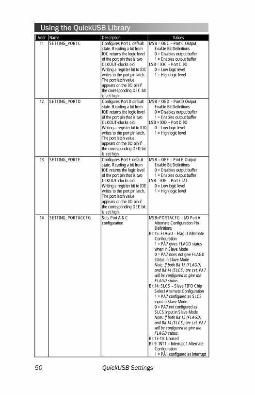
Using the QuickUSB Library Addr Name Description Values 11 SETTING_PORTC Configures Port C default
state. Reading a bit from IOC returns the logic level of the port pin that is two CLKOUT-clocks old. Writing a register bit to IOC writes to the port pin latch. The port latch value appears on the I/O pin if the corresponding OEC bit is set high.
MSB = OEC – Port C Output Enable Bit Definitions
0 = Disables output buffer 1 = Enables output buffer LSB = IOC – Port C I/O 0 = Low logic level 1 = High logic level
12 SETTING_PORTD Configures Port D default state. Reading a bit from IOD returns the logic level of the port pin that is two CLKOUT-clocks old. Writing a register bit to IOD writes to the port pin latch. The port latch value appears on the I/O pin if the corresponding OED bit is set high.
MSB = OED – Port D Output Enable Bit Definitions
0 = Disables output buffer 1 = Enables output buffer LSB = IOD – Port D I/O 0 = Low logic level 1 = High logic level
13 SETTING_PORTE Configures Port E default state. Reading a bit from IOE returns the logic level of the port pin that is two CLKOUT-clocks old. Writing a register bit to IOE writes to the port pin latch. The port latch value appears on the I/O pin if the corresponding OEE bit is set high.
MSB = OEE – Port E Output Enable Bit Definitions
0 = Disables output buffer 1 = Enables output buffer LSB = IOE – Port E I/O 0 = Low logic level 1 = High logic level
14 SETTING_PORTACCFG Sets Port A & C configuration
MSB=PORTACFG – I/O Port A Alternate Configuration Pin Definitions
Bit 15: FLAGD – Flag D Alternate Configuration
1 = PA7 gives FLAGD status when in Slave Mode
0 = PA7 does not give FLAGD status in Slave Mode
Note: If both Bit 15 (FLAGD) and Bit 14 (SLCS) are set, PA7 will be configured to give the FLAGD status.
Bit 14: SLCS – Slave FIFO Chip Select Alternate Configuration
1 = PA7 configured as SLCS input in Slave Mode
0 = PA7 not configured as SLCS input in Slave Mode
Note: If both Bit 15 (FLAGD) and Bit 14 (SLCS) are set, PA7 will be configured to give the FLAGD status.
Bit 13-10: Unused Bit 9: INT1 – Interrupt 1 Alternate
Configuration 1 = PA1 configured as interrupt
50 QuickUSB Settings

Using the QuickUSB Library Addr Name Description Values
input 0 = PA1 not configured as
interrupt input (default) Note: INT1 is not currently used Bit 8: INT0 – Interrupt 0 Alternate
Configuration 1 = PA0 configured as interrupt
input 0 = PA0 not configured as
interrupt input (default) Note: INT0 is not currently used LSB=PORTCCFG – I/O Port C
Alternate Configuration Pin Definitions
Bit 7-0: GPIFA7:0 – Enable GPIF Address Pins
1 = Set these pins to “1” to configure this port to output the GPIF Address
0 = Set these pins to “0” to configure this port as Port C
15 SETTING_PINFLAGS Sets FIFO pin flag configuration
MSB=PINFLAGSAB – Slave FIFO FLAGA and FLAGB Pin Configuration
Bit 15-12: FLAGB – FLAGB Show the status of the FIFO Flag selected by programming these bits with the code given below.
Bit 11-8: FLAGA – FLAGA shows the status of the FIFO Flag selected by programming these bits with the code given below.
LSB=PINFLAGSCD Bit 7-4: FLAGD – FLAGD shows
the status of the FIFO Flag selected by programming these bits with the code given below.
Bit 3-0: FLAGC – FLAGC shows the status of the FIFO Flag selected by programming these bits with the code given below.
FIFO Flag Select Codes: ‘0000’ = FLAGA = PF, FLAGB =
FF, FLAGC = EF, FLAGD = EP2PF. The Endpoint FIFO of the PF, FF, or EF is selected by the FIFOADR[1:0] pins.
‘0001’, ‘0010’, ‘0011’ = Reserved
‘0100’ = EP2PF ‘0101’ = EP4PF ‘0110’ = EP6PF ‘0111’ = EP8PF ‘1000’ = EP2EF ‘1001’ = EP4EF ‘1010’ = EP6EF ‘1011’ = EP8EF ‘1100’ = EP2FF ‘1101’= EP4FF ‘1110’ = EP6FF
QuickUSB Settings 51

Using the QuickUSB Library Addr Name Description Values
‘1111’ = EP7FF 17 SETTING_VERSIONSPEED Returns the CY7C68013
hardware revision and USB bus speed.
MSB= Hardware revision Bits 15-8: 00000000=CY7C68013 Rev A/B 00000001=CY7C68013A Rev A 00000010=CY7C68013 Rev C/D 00000100=CY7C68013 Rev E LSB= USB bus speed Bit 7: 0=Full Speed (12Mbps) 1=High Speed (480Mbps) Bit 6-0: Reserved for future use
Table 10 - QuickUSB Settings
QuickUsbReadSetting Purpose
To read QuickUSB module settings.
Parameters hDevice: A HANDLE that was returned from a call to QuickUsbOpen. address: A WORD containing the setting address (number) setting: A PWORD pointing to a variable in which to place the value of
the setting if successful.
Returns A LONG that is non-zero and the setting value in ‘setting’ if successful, zero (0) otherwise.
Notes None.
QuickUsbWriteSetting Purpose
To write QuickUSB module settings.
Parameters hDevice: A HANDLE that was returned from a call to QuickUsbOpen. address: A WORD containing the setting address. setting: A WORD containing the new setting value.
Returns A LONG that is non-zero on success, zero (0) on failure.
Notes None
52 QuickUSB Settings

Using the QuickUSB Library
QuickUsbReadDefault Purpose
To read QuickUSB module defaults. The defaults are non-volatile and are read into the settings table on power up.
Parameters hDevice: A HANDLE that was returned from a call to QuickUsbOpen. address: A WORD containing the default address (number) setting: A PWORD pointing to a variable in which to place the value of
the default if successful.
Returns A LONG that is non-zero on success, zero (0) on failure.
Notes None.
QuickUsbWriteDefault Purpose
To write QuickUSB module defaults. The defaults are non-volatile and are read into the settings table on power up.
Parameters hDevice: A HANDLE that was returned from a call to QuickUsbOpen. address: A WORD containing the default address (number) setting: A WORD containing the new default value.
Returns A LONG that is non-zero on success, zero (0) on failure.
Notes None.
QuickUSB Settings 53

Using the QuickUSB Library
FPGA Configuration The QuickUSB Plug-In module can configure SRAM-based FPGA devices over the USB. The default FPGATYPE is Passive Serial. For more information on changing the FPGA type, see the SETTING_FPGATYPE setting of the ‘Settings’ section of this document.
You must convert your FPGA configuration file to binary image format for use with QuickUSB. Altera binary files are of type RBF and Xilinx are of type BIT. If you are configuring multiple devices, they must be daisy-chained and the configuration files combined in the conversion process into a single binary file.
To configure an FPGA, follow these steps:
1. Call QuickUsbStartFpgaConfiguration. This resets the FPGA and starts the configuration process.
2. Open the binary FPGA configuration file and read a block into a buffer.
3. Call QuickUsbWriteFpgaData and pass in the data from the file. Repeat this process until the entire file is sent. Of course, the last block will probably be less than the maximum block size. In addition, if you need to restart the configuration process for some reason, you can call restart at step 1 at any time. Be sure to close the binary FPGA configuration file when you are done.
4. Call QuickUsbIsFpgaConfigured. If the ‘isConfigured’ parameter gets set to ‘1’, the FPGA was correctly configured. If not, try again starting at step 1.
QuickUsbStartFpgaConfiguration Purpose
Start the process of FPGA configuration. If the FPGA is in the process of being configured, the process will restart. If the FPGA is already configured, it will be reset and reconfigured.
Parameters hDevice: A HANDLE that was returned from a call to QuickUsbOpen.
Returns A LONG that is non-zero on success, zero (0) on failure.
Notes None
54 FPGA Configuration
Using the QuickUSB Library
QuickUsbWriteFpgaData Purpose
Sends FPGA configuration data to the FPGA using the QuickUSB FPGA configuration port.
Parameters hDevice: A HANDLE that was returned from a call to QuickUsbOpen. data: A PBYTE pointing to a BYTE buffer containing the FPGA
configuration data. See notes. length: A ULONG containing the length of the data in bytes. See
notes.
Returns A LONG that is non-zero on success, zero (0) on failure.
Notes • The maximum data length is 64. • A call to QuickUsbStartFpgaConfiguration must precede FPGA
configuration.
QuickUsbIsFpgaConfigured Purpose
Check to see if the FPGA is configured.
Parameters hDevice: A HANDLE that was returned from a call to QuickUsbOpen. isConfigured: A PWORD pointing to a WORD in which to write the
configuration status of the FPGA connected to the QuickUSB FPGA configuration port. 1 = the FPGA is configured (CONF_DONE = ‘1’), 0 = the FPGA is not configured (CONF_DONE = ‘0’).
Returns A LONG that is non-zero on success, zero (0) on failure.
Notes • The value of the the CONF_DONE line is returned as bit 0 of
'isConfigured'.
FPGA Configuration 55

Using the QuickUSB Library
High-Speed Parallel Port
QuickUsbReadCommand Purpose
Read a block of command values from the high-speed parallel port using the QuickUSB module.
Parameters hDevice: A HANDLE that was returned from a call to QuickUsbOpen. address: A WORD containing the address. This address is the starting
value of the HSPP address bus. If address bit 14 is set (1), then the address bus will not be driven. If address bit 15 is set (1), then the address will not be incremented after each read.
data: A pointer to a buffer in which to place data read from the high-speed parallel port. See notes.
length: A PWORD pointing to a WORD containing the number of bytes to read from the high-speed parallel port on input and the number of bytes read on return. See notes.
Returns A LONG that is non-zero on success, zero (0) on failure.
Notes • The maximum length is 64 bytes. • The data buffer can contain data values of any type. • Commands are transferred over the high-speed parallel port with the
CMD_DATA line set to ‘1’. • The address bus behavior for data transfers is defined by the
SETTING_DATAADDRESS setting.
56 High-Speed Parallel Port
Using the QuickUSB Library
QuickUsbWriteCommand Purpose
Write a block of command values to the high-speed parallel port using the QuickUSB module.
Parameters hDevice: A HANDLE that was returned from a call to QuickUsbOpen. address: A WORD containing the address. This address is the starting
value of the HSPP address bus. If address bit 14 is set (1), then the address bus will not be driven. If address bit 15 is set (1), then the address will not be incremented after each write.
data: A pointer to a buffer containing the data to write to the high-speed parallel port. See notes.
length: A WORD containing the number of bytes to write to the high-speed parallel port. See notes.
Returns A LONG that is non-zero on success, zero (0) on failure.
Notes • The maximum length is 64 bytes. • The data buffer can receive data values of any type. • Commands are transferred over the high-speed parallel port with the
CMD_DATA line set to ‘1’. • The address bus behavior for data transfers is defined by the
SETTING_DATAADDRESS setting.
High-Speed Parallel Port 57

Using the QuickUSB Library QuickUsbReadData Purpose
Read a block of data values from the high-speed parallel port using the QuickUSB module.
Parameters hDevice: A HANDLE that was returned from a call to QuickUsbOpen. data: A pointer to a buffer in which to place data values read from
the HSPP. See notes. length: A PULONG to a ULONG containing the number of bytes to
read from the HSPP. See notes.
Returns A LONG that is non-zero on success, zero (0) on failure.
Notes • The maximum length is 16 megabytes (16777216 bytes). • The data buffer can receive data values of any type. • This function has a call latency of approximately 1ms for full-speed
connections and 250 us for hi-speed connections. • In order to obtain the maximum performance, call this function with
the largest appropriate length value. Each call to this function will incur one call latency delay regardless of the transfer size. So to minimize delays that erode the data transfer rate, make the transfers as large as possible for your application.
• In master mode, data values are transferred over the high-speed parallel port with the CMD_DATA line set to ‘0’.
• In slave mode, the USB will wait for ‘length’ transfers to occur before returning. If the target interface does not write length transfers to the slave FIFOs, the call will return with a value of 0 and set the last error status to QUICKUSB_ERROR_TIMEOUT after the timeout value specified by the QuickUsbSetTimeout function.
• The address bus behavior for data transfers is defined by the SETTING_DATAADDRESS setting.
58 High-Speed Parallel Port

Using the QuickUSB Library
QuickUsbWriteData Purpose
Write a block of data values to the high-speed parallel port using the QuickUSB module.
Parameters hDevice: A HANDLE that was returned from a call to QuickUsbOpen. data: A pointer to a block of data values to write to the HSPP. See
notes. length: A ULONG containing the number of bytes to write to the
HSPP. See notes.
Returns A LONG that is non-zero on success, zero (0) on failure.
Notes • The maximum length is 16 megabytes (16777216 bytes). • The data buffer can contain data values of any type. • In master mode, data values are transferred over the high-speed
parallel port with the CMD_DATA line set to ‘0’. • In slave mode, the USB will hang and wait for ‘length’ transfers to
occur before returning. If the target interface does not read length transfers from the slave FIFOs, the call will return with a value of 0 and set the last error status to QUICKUSB_ERROR_TIMEOUT after the timeout value specified by the QuickUsbSetTimeout function.
• The address bus behavior for data transfers is defined by the SETTING_DATAADDRESS setting.
High-Speed Parallel Port 59
Using the QuickUSB Library QuickUsbReadDataAsync Purpose
Read a block of data values from the high-speed parallel port using an asynchronous function call.
Parameters hDevice: A HANDLE that was returned from a call to QuickUsbOpen. data: A pointer to a buffer in which to place data read from the
HSPP. See notes. length: A PULONG containing the number of bytes to read from the
HSPP. See notes. transaction: A PBYTE to a BYTE in which to place the transaction identifier
required by QuickUsbAsyncWait.
Returns A LONG that is non-zero on success, zero (0) on failure.
Notes • QuickUSB asynchronous function calls return immediately and must
be followed by a call to QuickUsbAsyncWait to determine when the transaction actually completes and to free internal buffers used by the operating system. Failure to follow this procedure will result in a memory leak and an eventual system crash.
• The maximum length is 16 megabytes (16777216 bytes. • The data buffer can receive data values of any type. • In master mode, data values are transferred over the high-speed
parallel port with the CMD_DATA line set to ‘0’. • In slave mode, the USB will hang and wait for ‘length’ transfers to
occur before returning. If the target interface does not read length transfers from the slave FIFOs, the call will return with a value of 0 and set the last error status to QUICKUSB_ERROR_TIMEOUT after the timeout value specified by the QuickUsbSetTimeout function.
• The address bus behavior for data transfers is defined by the SETTING_DATAADDRESS setting.
• There is a global maximum of 253 asynchronous reads and writes outstanding at any time for all QuickUSB modules in the system.
• This function is not yet supported for Linux-based systems.
60 High-Speed Parallel Port
Using the QuickUSB Library
QuickUsbWriteDataAsync Purpose
Write a block of data values to the high-speed parallel port using an asynchronous function call.
Parameters hDevice: A HANDLE that was returned from a call to QuickUsbOpen. data: A pointer to a block of data values to write to the HSPP. See
notes. length: A ULONG containing the number of bytes to write to the
HSPP. See notes. transaction: A PBYTE to a BYTE in which to place the transaction identifier
required by QuickUsbAsyncWait.
Returns A LONG that is non-zero on success, zero (0) on failure.
Notes • QuickUSB asynchronous function calls return immediately and must
be followed by a call to QuickUsbAsyncWait to determine when the transaction actually completes and to free internal buffers used by the operating system. Failure to follow this procedure will result in a memory leak and an eventual system crash.
• The maximum length is 16 megabytes (16777216 bytes. • The data buffer can receive data values of any type. • In master mode, data values are transferred over the high-speed
parallel port with the CMD_DATA line set to ‘0’. • In slave mode, the USB will hang and wait for ‘length’ transfers to
occur before returning. If the target interface does not read length transfers from the slave FIFOs, the call will return with a value of 0 and set the last error status to QUICKUSB_ERROR_TIMEOUT after the timeout value specified by the QuickUsbSetTimeout function.
• The address bus behavior for data transfers is defined by the SETTING_DATAADDRESS setting.
• There is a global maximum of 253 asynchronous reads and writes outstanding at any time for all QuickUSB modules in the system.
• This function is not yet supported for Linux-based systems.
High-Speed Parallel Port 61
Using the QuickUSB Library QuickUsbAsyncWait Purpose
Wait for an asynchronous transfer to complete.
Parameters hDevice: A HANDLE that was returned from a call to QuickUsbOpen. length: An PULONG that returns the number of bytes that were
transferred as a result of the asynchronous function call. If the asynchronous function call is still pending, ‘length’ will be set to 0. This function must be called until ‘length’ is non-zero otherwise, the driver will not release its internal buffers thus causing a memory leak and an eventual system crash (Blue Screen of Death). If the asynchronous function call has completed, the number of bytes requested will be stored in ‘length’ and all internal buffers will be released.
transaction: A BYTE transaction identifier returned by QuickUsbReadDataAsync or QuickUsbWriteDataAsync.
immediate: A BYTE value. If nonzero, the driver will not wait the default timeout value for the transaction to complete. If zero, the driver will wait the default timeout period for the transaction to complete.
Returns • A LONG that is non-zero on success, zero (0) on failure.
If the asynchronous function call is still pending, ‘length’ will be set to 0. This function must be called until ‘length’ is non-zero. If this is not done, the driver will not release its internal buffers thus causing a memory leak and an eventual system crash (Blue Screen of Death). If the asynchronous function call has completed, the number of bytes requested will be stored in ‘length’.
Notes • This function is not yet supported for Linux-based systems.
62 High-Speed Parallel Port

Using the QuickUSB Library
General-Purpose I/O There are five (5) 8-bit general-purpose I/O ports on the QuickUSB module named A-E. Of those, some may be used for other purposes. Port E is used for the FPGA configuration and SPI functions, so if either of these functions is used in your design, some of the pins on port E will be consumed.
Other than that, the general-purpose I/O ports are just like I/O ports you would find on a microcontroller. The functions provided by the QuickUSB Library give you the capability to set the direction of each pin, read and write to the ports on a byte wide basis.
QuickUsbReadPortDir Purpose
Read the data direction of each data port bit for the specified port.
Parameters hDevice: A HANDLE that was returned from a call to QuickUsbOpen. address: A BYTE containing the port address. Ports are addressed 0 to
4 corresponding to port A-E. data: A PBYTE to a BYTE in which to place the data direction bit
values. Each bit in data corresponds to data bits of the specified port. A data direction bit value of 0=input and 1=output (i.e. 0x03 means that bits 0 and 1 are outputs and bits 2-7 are inputs).
Returns A LONG that is non-zero on success, zero (0) on failure.
Notes None
QuickUsbWritePortDir Purpose
Set the data direction of each data port bit for the specified port.
Parameters hDevice: A HANDLE that was returned from a call to QuickUsbOpen. address: The port address. Ports are addressed 0 to 4 corresponding
to port A-E. data: A byte that contains the data direction bit values. Each bit in
data corresponds to data bits of the specified port. A data direction bit value of 0=input and 1=output.
Returns A LONG that is non-zero on success, zero (0) on failure.
Notes None
General-Purpose I/O 63
Using the QuickUSB Library QuickUsbReadPort Purpose
Read a series of bytes from the specified port.
Parameters hDevice: A HANDLE that was returned from a call to QuickUsbOpen. address: The port address. Ports are addressed 0 to 4 corresponding
to port A-E. data: A pointer to an array of bytes in which to place the data. This
buffer must be at least ‘length’ bytes long. length: A pointer to the number of bytes to read from the port. The
bytes are read sequentially. The maximum length is 64 bytes.
Returns A non-zero value if successful, 0 otherwise. Also returns the read value in value if successful. Otherwise value is not modified.
Notes This function reads an array of values from the specified port. There is no synchronization mechanism provided so the values are read as fast as the microcontroller can read them.
QuickUsbWritePort Purpose
Write a series of bytes to the specified port.
Parameters hDevice: A HANDLE that was returned from a call to QuickUsbOpen. address: The port address. Ports are addressed 0 to 4 corresponding
to port A-E. data: A pointer to an array of bytes to send out the port. This buffer
must be at least ‘length’ bytes long. length: A pointer to the number of bytes to write to the port. The
bytes are written sequentially. The maximum length is 64 bytes.
Returns A non-zero value if successful, 0 otherwise.
Notes This function writes an array of values from the specified port. Of course, the most common array is an array of 1 byte. However, writing multiple bytes out makes it possible to clock out a series of bits if one of the bits is used as the clock. Up to 32 clock cycles can be generated using this technique.
64 General-Purpose I/O
Using the QuickUSB Library
RS-232 The RS-232 ports are interrupt-driven for transmit and receive. The QuickUSB RS232 receive buffers are 128 bytes deep, so your software just needs to service these buffers often enough to make sure they do not overflow.
QuickUsbSetRs232BaudRate Purpose
Set the baud rate for both serial ports. Baud rates are programmable from 4800 to 230k baud. This function sets the baud rate of both serial ports. It is not possible to set the baud rate of each serial port independently.
Parameters hDevice: A HANDLE that was returned from a call to QuickUsbOpen. baudRate: An unsigned long integer (32-bits) containing the baud rate in
bits per second.
Returns A non-zero value if successful, 0 otherwise.
Notes None
QuickUsbGetNumRS232 Purpose
Read the number of characters waiting in the receive buffer.
Parameters hDevice: A HANDLE that was returned from a call to QuickUsbOpen. portNum: The serial port number. Serial port 0 (P1) = 0, serial port 1
(P2) = 1. length: A pointer to the number of characters to read. Set to the
number of characters actually read on return.
Returns A non-zero value and the number of outstanding characters if successful, 0 otherwise.
Notes None.
RS-232 65

Using the QuickUSB Library QuickUsbFlushRS232 Purpose
Flush the RS232 port transmit and receive buffers.
Parameters hDevice: A HANDLE that was returned from a call to QuickUsbOpen. portNum: The serial port number. Serial port 0 (P1) = 0, serial port 1
(P2) = 1.
Returns A non-zero value if successful, 0 otherwise.
Notes None.
QuickUsbReadRS232 Purpose
Read a block of characters from the interrupt receive buffer of the specified QuickUSB serial port.
Parameters hDevice: A HANDLE that was returned from a call to QuickUsbOpen. portNum: The serial port number. Serial port 0 (P1) = 0, serial port 1
(P2) = 1. data: A pointer to a buffer in which to place the data. The buffer
must be at least 128 bytes long. length: A pointer to the number of characters to read. Set to the
number of characters actually read on return.
Returns A non-zero value, the data and the length if successful, 0 otherwise.
Notes • The interrupt buffer is 128 bytes deep. If length is set to more than
128, the routine will hang and wait for the specified number of characters to be read from the port before returning.
66 RS-232
Using the QuickUSB Library
QuickUsbWriteRS232 Purpose
Write a block of characters to the specified QuickUSB serial port.
Parameters hDevice: A HANDLE that was returned from a call to QuickUsbOpen. portNum: The serial port number. Serial port 0 (P1) = 0, serial port 1
(P2) = 1. data: A pointer to a buffer containing the data. length: The number of characters to write.
Returns A non-zero value if successful, 0 otherwise.
Notes • None
RS-232 67
Using the QuickUSB Library
I2C-Compatible Port The QuickUSB I2C-compatible port is a master-only bus controller. The bus runs at approximately 100Khz. Address 1 is reserved. The bus speed may be changed with the SETTING_I2CTL setting.
QuickUsbReadI2c Purpose
None
Parameters hDevice: A HANDLE that was returned from a call to QuickUsbOpen. address: The device address. data: A pointer to a buffer in which to place the data. length: The length of the data buffer in bytes. The maximum length is
64 bytes.
Returns A non-zero value if successful, 0 otherwise. In addition, length is set the actual number of bytes read.
Notes None
QuickUsbWriteI2c Purpose
None
Parameters hDevice: A HANDLE that was returned from a call to QuickUsbOpen. address: The device address. data: A pointer to the data to send. length: The length of the data buffer in bytes. The maximum length is
64 bytes.
Returns A non-zero value if successful, 0 otherwise.
Notes None
68 I2C-Compatible Port
Using the QuickUSB Library
SPI-Compatible Port The QuickUSB module implements a ‘soft’ SPI port using pins on port E and optionally port A. These routines support from 1 to 10 devices with individual slave select lines for each device. The slave select lines are active low and are shown in Table 7 - QuickUSB Pin Definitions. The signals are MOSI, SCK, MISO and nSS0-9. By default, data is shifted in and out MSbit to LSbit. The bit shift order can be configured by changing Bit 0 of the SETTINGS_SPICONFIG setting. The SPI bus runs at approximately 500Kbps. You can learn more about QuickUSB’s SPI interface in the SPI section of this document.
QuickUsbReadSpi Purpose
Read a block of bytes from the specified SPI slave port.
Parameters hDevice: A HANDLE that was returned from a call to QuickUsbOpen. portNum: The SPI device address (nSS line) to read from. data: A pointer to a buffer in which to place the received data. length: A pointer to the number of bytes to read. The maximum
length is 64 bytes.
Returns A non-zero value if successful, 0 otherwise. In addition, the data buffer is filled with the received data and the length is set to the number of bytes actually received on success. Both data and length are left unchanged if the function failed.
Notes This function applies a logic low (0) to the MOSI port while reading in the data.
QuickUsbWriteSpi Purpose
Write a block of bytes to the specified SPI slave port.
Parameters hDevice: A HANDLE that was returned from a call to QuickUsbOpen. portNum: The SPI device address (nSS line) to write to. data: A pointer to the data to send. length: The number of bytes to send. The maximum length is 64
bytes.
Returns A non-zero value if successful, 0 otherwise.
Notes This function ignores data received at the MISO pin while writing. If you need to capture MISO data while writing, you should use the QuickUsbWriteReadSpi function.
SPI-Compatible Port 69
Using the QuickUSB Library QuickUsbWriteReadSpi Purpose
Simultaneously write and read a block of data to and from the specified SPI slave port.
Parameters hDevice: A HANDLE that was returned from a call to QuickUsbOpen. portNum: The SPI device address (nSS line) to write to and read from data: A pointer to the buffer that contains the data to send and in
which to place the received data. length: The number of bytes to send and receive. The maximum
length is 64 bytes.
Returns A non-zero value if successful, 0 otherwise. In addition, the data buffer is filled with the received data and the length is set to the number of bytes actually received on success. Both data and length are left unchanged if the function failed.
Notes This function uses the data buffer for both writing data to the SPI and to store read data from the SPI. Therefore, the data buffer will always be overwritten on each call to this function.
70 SPI-Compatible Port
Index
Index address bus .................................. 4 architecture................................... 1 ASYNC..........................................19 asynchronous function calls........ 2 bus
address .................................... 4 high-speed parallel.................. 4
CMD_DATA .................................... 5 current limiting ............................. 3 defaults
firmware ................................... 4 delay
interpacket............................... 2 device ............................................ 1 endpoint ........................................ 1 EZ USB FX2 ................................... 3 FET
power........................................ 3 frame ............................................. 2 full speed ...................................... 2 function
asynchronous .......................... 2 GPIF ............................................... 5 Ground........................................... 3 Hardware....................................... 3 High Speed Parallel Port .............. 4 Hi-Speed........................................ 2 host................................................ 1 HSPP.............................................. 4 hub
USB........................................... 3 I/O connections
GPIF master mode................... 6 slave FIFO...............................16
I/O model block handshake ...................12 fifo handshake......................... 9 full handshake.......................11 pipeline...................................14 slave FIFO...............................16 synchronous slave FIFO ........17
I/O Model simple....................................... 7
I/O Models master mode............................ 6
I/O Pins
unused ......................................4 IFCLK..............................................5 interpacket delay...........................2 interrupt .........................................1 latency............................................2 master ............................................1 mode
GPIF master ..............................5 OE 5 pipe.................................................1 Power .............................................3 power supply
external .....................................3 QuickUsbReadCommand .............5 QuickUsbReadData.......................5 QuickUsbWriteCommand .............5 QuickUsbWriteData.......................5 READY ......................................... 11 REN.................................................5 settings
default.......................................4 SETTING_DATAADDRESS.........4 SETTING_FIFO_CONFIG ....4, 16 SETTING_SLAVEFIFOFLAGS.. 16
Simple I/O Model ..........................7 Slave FIFO I/O Models ............... 16 SW_PG ...........................................3 switch
power ........................................3 synchronous ..................................5 throughput .....................................2 timebase ........................................2 timing parameters
GPIF master mode ...................6 timing Parameters
synchronous slave FIFO........ 18 TPS2051A......................................3 transfer latency .............................2 transfers
command..................................5 data ...........................................5
USB.................................................1 VBUS...............................................3 web site..........................................1 WEN................................................5 WORDWIDE....................................4
SPI-Compatible Port 71