scan test coverage improvement via …eprints.usm.my/39652/1/muhammad_redzwan_bin... · faults that...
TRANSCRIPT
SCAN TEST COVERAGE IMPROVEMENT VIA
AUTOMATIC TEST PATTERN GENERATION
(ATPG) TOOL CONFIGURATION
By
MUHAMMAD REDZWAN BIN SALEHUDDIN
A Dissertation submitted for partial fulfilment of the
requirement for the degree of Master of Science
(Microelectronic Engineering)
August 2017

ii
ACKNOWLEDGEMENT
In the name of Allah, the Beneficent, the Compassionate, and the Most Merciful.
Alhamdulillah, all praises to Allah for the strengths and His blessings in my journey
of completing this thesis. I would also like to express my deepest appreciation to all
who provided me with the support and help so that I was able to complete this project
especially to my parents who were very understanding and provided their blessings
throughout the project.
A special thanks to my supervisor, Dr. Mohamad Adzhar Md Zawawi, who had guided
me in completing this thesis and project by stimulating suggestions, providing
guidelines and encouragement. His invaluable help of constructive comments and
suggestions throughout the experimental and thesis works have contributed to the
success of this project.
I would also like to acknowledge with much appreciation the helpful role of the staff
of USAINS Holding Sdn Bhd (USAINS), who had provided the logistics and supports
to ease the completion of this project and thesis.
Last but not least, I would like to express my appreciation again to everyone including
my family and friends who had involved directly or indirectly, for the supports and
ideas in completing this project. Your kindness is very much appreciated. Thank you.

iii
TABLE OF CONTENTS
ACKNOWLEDGEMENT ..................................................................................................... ii
TABLE OF CONTENTS ..................................................................................................... iii
LIST OF FIGURES ............................................................................................................... vi
LIST OF TABLES .............................................................................................................. viii
LIST OF ABBREVIATIONS ............................................................................................... ix
ABSTRAK ............................................................................................................................... x
ABSTRACT ............................................................................................................................ xi
CHAPTER 1: INTRODUCTION .......................................................................................... 1
1.1 Background ..................................................................................................................... 1
1.2 Problem Statements ........................................................................................................ 5
1.3 Project Objectives ........................................................................................................... 7
1.4 Project Scope .................................................................................................................. 8
1.5 Project Contribution ........................................................................................................ 8
1.6 Thesis Outline ................................................................................................................. 9
CHAPTER 2: LITERATURE REVIEW............................................................................ 10
2.1 Introduction ................................................................................................................... 10
2.2 Relevant Theories ......................................................................................................... 11
2.2.1 VLSI Development Process ................................................................................... 11
2.2.2 VLSI Testing ......................................................................................................... 12
2.2.3 Yield and Reject Rate ............................................................................................ 15
2.2.4 Automatic Test Equipment (ATE) ......................................................................... 16
2.2.5 Design for Test (DFT) ........................................................................................... 17
2.2.6 Scan Design and Scan Design Overview ............................................................... 19
2.2.7 Scan Mode of Operations ...................................................................................... 20
2.2.8 Mux-D Scan Cell ................................................................................................... 22
2.2.9 Scan Design Rules ................................................................................................. 22
2.2.10 Fault Models ........................................................................................................ 23
2.2.11Targeted Fault Models of Scan Tests .................................................................. 24
iv
2.2.12 Fault Simulation ................................................................................................... 27
2.2.13 Scan Test Patterns Generation ............................................................................. 27
2.2.14 Scan Test Coverage ............................................................................................. 28
2.3 Previous Design-Based SCAN Coverage Improvement Researches ............................ 30
2.3.1 Combining the Staggered Single-Capture Scheme and the One-Hot Single-
Capture Scheme for Detecting Structural Faults ........................................................... 30
2.3.2 Multiple Scan-Enable Signals ............................................................................... 31
2.3.3 Delay Test Scan Flip-Flop (DTSFF) ..................................................................... 32
2.3.4 Dummy Flip-Flops and Additional Multiplexer ................................................... 38
2.3.5 SCAN Chain Reordering and Dummy Latches .................................................... 42
2.4 Summary ....................................................................................................................... 43
CHAPTER 3: METHODOLOGY....................................................................................... 45
3.1 Introduction ................................................................................................................... 45
3.2 Overall Project Flow ..................................................................................................... 46
3.3 Project Type .................................................................................................................. 47
3.4 Materials and Equipment .............................................................................................. 47
3.5 Test Pattern Generation ................................................................................................. 55
3.6 Stuck-At Fault Model ................................................................................................... 58
3.7 Parallel-Pattern Fault Simulation .................................................................................. 61
3.8 Scan Chains ................................................................................................................... 63
3.9 ATPG Process ............................................................................................................... 64
3.10 Design of Experiment (DOE) ..................................................................................... 68
3.11 Experimental Setup ..................................................................................................... 68
3.12 Sampling Methods and Measurements Techniques .................................................... 70
3.13 Data Compilation and Analysis .................................................................................. 72
3.14 Problems Anticipated and Workaround ...................................................................... 73
3.15 Summary ..................................................................................................................... 74
CHAPTER 4: RESULTS AND DISCUSSIONS ................................................................ 75
4.1 Introduction ................................................................................................................... 75
4.2 Experimental Results and Discussions ......................................................................... 75
4.3 Real Silicon Validation ................................................................................................. 85
4.4 Summary ....................................................................................................................... 87

v
CHAPTER 5: CONCLUSIONS AND FUTURE WORKS ............................................... 90
5.1 Conclusions ................................................................................................................... 90
5.2 Future Works ................................................................................................................ 91
REFERENCES...................................................................................................................... 92
APPENDIX A ........................................................................................................................ 96
APPENDIX B ...................................................................................................................... 102
APPENDIX C ...................................................................................................................... 103

vi
LIST OF FIGURES
Figure 1.1: A Typical SCAN Cell………………………………………………..……3
Figure 1.2: Mux-D Full SCAN Circuit……………………………………………..…4
Figure 2.1: Basic Testing Approach………………………………………………....13
Figure 2.2: VLSI Development Process……………………………………………..13
Figure 2.3: Testing a Normal Sequential Circuit for Fault, f………………….……..21
Figure 2.4: Grouping of Flip-Flops with Two Scan Enable Signals………….………31
Figure 2.5: The Basic DTSFF………………………………………………………..33
Figure 2.6: Enhanced DTSFF………………………………………………………..34
Figure 2.7: Multiplexer Based Scan Flip-flop………………………………………..35
Figure 2.8: DTSFF Implemented using an AOI (1, 2)………………………….…….36
Figure 2.9: Six Transistor AOI (1, 2) Gate……………………………………….…..36
Figure 2.10: (a) Example Circuit (b) Utilization of Dummy Flip-Flop………………38
Figure 2.11: Additional Multiplexer Added in Front of Scan Cell……………….….40
Figure 2.12: Dual Enhanced Scan Flip-Flop…………………………………………41
Figure 2.13: Transition-Launch Flip-Flop…………………………………...………41
Figure 3.1: Overall Project Flow...……………………………………………….….46
Figure 3.2: EDT Architecture…………………………………………………….….48
Figure 3.3: Stuck-At Test Patterns Mechanism Illustration…………………………51
Figure 3.4: Waveform Sequence for Stuck-At Test Patterns………………………..51
Figure 3.5: Full Chip Block Diagram Representation of the Tested Die……………54
Figure 3.6: Complex Circuit Design………………………………………………...57

vii
Figure 3.7: Example of a Stuck-At 0 Fault at Fault Site, x1…………………….……59
Figure 3.8: Example of an Undetectable Fault for a Stuck-At 0 at Fault Site……….60
Figure 3.9: Example Circuit Illustrating Parallel-Pattern Fault Simulation ……..….62
Figure 3.10: Scan Chain Structure in a Sequential Circuit………………………......63
Figure 3.11: ATPG Process…………………………………………..………….…..64
Figure 4.1: Graph of Test Coverage for each Stepping in Setup 1………….……..…77
Figure 4.2: Test Patterns Count for each Stepping in Setup 1……………….………78
Figure 4.3: Test Coverage for Different Abort Limit Value in Setup 2……….….….80
Figure 4.4: Test Patterns Count for Different Abort Limit Value in Setup 2………..81
Figure 4.5: ATPG Runtime for Different Abort Limit Value in Setup 2……………81
Figure 4.6: Graph of Test Coverage for each Stepping in Setup 3…………………..83
Figure 4.7: Test Patterns Count for each Stepping in Setup 3………………...….….84
Figure 4.8: ATPG Runtime for each Stepping in Setup 3……………………..….…85
Figure 4.9: Shmoo Plot of Real Silicon Validation of the Test Patterns Generated….87

viii
LIST OF TABLES
Table 2.1: Typical Scan Design Rules………………………………………………23
Table 2.2: Operation Mode of Two Scan Enable……………………………………37
Table 2.3: Transition-Launch Flip-Flop Mode of Operations……………………….42
Table 2.4: Summary of Previous Design-Based Researches Reviewed………….….44
Table 3.1: Tested Circuit Parameters…………………………….…………………..53
Table 3.2: Response of Parallel-Pattern Fault Simulation for Figure 3.5….…….…..62
Table 3.3: List of DRC in Tessent Tool………………………….…………………..65
Table 3.4: Experimental Setup 1………………………………….………….…..….69
Table 3.5: Experimental Setup 2………………………………….……..……..…….69
Table 3.6 Experimental Setup 3……………………………………….…….…….....70
Table 3.7: Fault Classes for Stuck-at Pattern Generation…………………..….…….71
Table 4.1: Experimental Result for Setup 1……………………..…….……..………75
Table 4.2: Experimental Result for Setup 2………….…………………….…..…….79
Table 4.3: Experimental Result for Setup 3……………………..……..…………….82

ix
LIST OF ABBREVIATIONS
ATE – Automatic Test Equipment
ATPG – Automatic Test Pattern Generation
CUT – Circuit under Test
DFT – Design for Testability
DOE – Design of Experiments
DSP – Digital Signal Processor
DTSFF – Delay Test Scan Flip - Flop
DUT – Die under Test
EDT – Embedded Deterministic Test
IC – Integrated Circuit
LOC – Launch on Capture
LOS – Launch on Shift
OS – Operating Systems
SE – Scan Enable
SEG – Scan Enable Group
SOC – Systems on Chip
SSF – Single Stuck-at Fault
TM – Test Mode
TR-TC – Test Resources – Test Coverage
VLSI – Very Large Scale Integration

x
PENAMBAHBAIKAN LIPUTAN UJIAN SCAN MELALUI KONFIGURASI
PERALATAN PENJANAAN CORAK UJIAN AUTOMATIK (ATPG)
ABSTRAK
Penambahbaikan liputan ujian scan dengan menggunakan konfigurasi peralatan
penjanaan corak ujian automatik (ATPG) dikaji. Meningkatkan liputan ujian adalah
penting dalam mengesan kerosakan pengilangan dalam industri semikonduktor supaya
produk yang berkualiti tinggi boleh dibekalkan kepada pengguna. Peralatan ATPG
yang digunakan adalah Mentor Graphics Tessent TestKompress (versi 2014.1). Kajian
ini telah dilakukan dengan memperkenalkan beberapa eksperimen menggunakan
pengubahsuaian terhadap arahan dan suis ATPG, memerhatikan peningkatan liputan
ujian dari laporan statistik yang dibekalkan semasa proses penjanaan corak ujian dan
menyediakan perbincangan yang berkaitan. Dengan pengubahsuaian arahan ATPG,
dijangka liputan ujian akan meningkat. Corak ujian scan yang dijana adalah corak
ujian stuck-at. Berdasarkan eksperimen yang telah dilakukan, perbandingan telah
dibuat pada bacaan liputan yang berbeza dan kaedah yang paling optimum dan aliran
ATPG telah ditentukan. Aliran paling optimum telah memberi peningkatan 0.91%
dalam liputan ujian. Corak ujian yang dihasilkan telah ditukar dan diuji menggunakan
peralatan ujian automatik (ATE) untuk memerhati prestasinya pada silikon sebenar.
Peningkatan liputan ujian menggunakan peralatan ATPG dan bukannya kaedah
berasaskan reka bentuk adalah penting sebagai penyelesaian alternatif yang lebih cepat
bagi jurutera ujian untuk menyediakan kandungan ujian berkualiti tinggi dalam
tempoh pembangunan produk yang singkat.

xi
SCAN TEST COVERAGE IMPROVEMENT VIA AUTOMATIC TEST
PATTERN GENERATION (ATPG) TOOL CONFIGURATION
ABSTRACT
The scan test coverage improvement by using automatic test pattern generation
(ATPG) tool configuration was investigated. Improving the test coverage is essential
in detecting manufacturing defects in semiconductor industry so that high quality
products can be supplied to consumers. The ATPG tool used was Mentor Graphics
Tessent TestKompress (version 2014.1). The study was done by setting up a few
experiments of utilizing and modifying ATPG commands and switches, observing the
test coverage improvement from the statistical reports provided during pattern
generation process and providing relatable discussions. By modifying the ATPG
commands, it can be expected to have some improvement in the test coverage. The
scan test patterns generated were stuck-at test patterns. Based on the experiments done,
comparison was made on the different coverage readings and the most optimized
method and flow of ATPG were determined. The most optimized flow gave an
improvement of 0.91% in test coverage which is acceptable since this method does not
involve a change in design. The test patterns generated were converted and tested using
automatic test equipment (ATE) to observe its performance on real silicon. The test
coverage improvement using ATPG tool instead of the design-based method is
important as a faster workaround for back-end engineers to provide high quality test
contents in such a short product development duration.

1
CHAPTER 1
INTRODUCTION
1.1 Background
The semiconductor industry globally has gone through tremendous
technological development and advancement the past few decades. In Malaysia, two
national wafer foundries namely Malaysian Institute of Microelectronics Systems
(MIMOS) Berhad and SILTERRA Malaysia Sdn Bhd (previously Wafer Technology
Malaysia Sdn Bhd) were established in 1985 and 1995 respectively[1][2] to indicate
the importance of semiconductor industry for this country. A handful number of multi-
national companies like Intel, Motorola, Texas Instruments and Broadcom are based
in Malaysia showing that Malaysia is moving up the value chain in this industry and
at the same time strengthening its economic growth. Strong collaboration between
industrial companies and public universities with state-of-the-art facilities had
generated more sophisticated knowledge for the advancement of the semiconductor
industry.
In this modern era, semiconductors and microelectronics are becoming the gist
for almost every technology that we have from computers, automotive,
communications to securities and even artificial intelligence-based applications [3].
Semiconductor companies are competing to be the leader in the industry by proposing
their own gauge for technological supremacy. For example, Intel are starting to make

2
10nm chips and with it they proposed a transistor density metric that it challenged
rivals to adopt [4]. The competition sparks a necessity for these companies to deliver
devices that are high quality and reliable. An important part in a device life cycle to
determine its reliability is the test and validation stage [5].
Devices fabricated from the foundry require testing to sort out the defective
devices. Testability is one of the most important factors that are considered during the
design life cycle along with reliability, speed, power consumption, cost and other
factors important for a customer [6]. Especially for optimization, testability is required
to provide information about the easiness of testing a given device under test (DUT)
with minimal error and in reasonable time. Production testing applies test patterns to
exercise devices for defect detection. Sometimes devices with a defect will pass all
applied tests. These are known as escapees. Those devices that fail at the customer site
are returned back to the manufacturer for analysis. However, if this ever happened it
would somehow tarnished the confidence of the customers toward the products from
the said manufacturer and this might affect future prospects for the manufacturer.
There are two types of tests, functional (or engineering) test and manufacturing
test. The functional test is used to verify the circuit functionality where analog, digital
and mixed-signal testing is done. This includes simulation and verification of design
logic. The manufacturing test is used to verify that the design has no manufacturing
defects. It does not verify how the silicon should behave as specified. There are
different types of manufacturing test which includes Built-in Self-Test (BIST),
memory test, functional test and SCAN test which is the focus in this project.
3
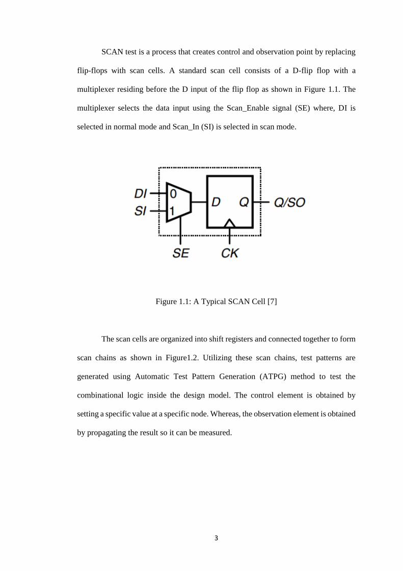
SCAN test is a process that creates control and observation point by replacing
flip-flops with scan cells. A standard scan cell consists of a D-flip flop with a
multiplexer residing before the D input of the flip flop as shown in Figure 1.1. The
multiplexer selects the data input using the Scan_Enable signal (SE) where, DI is
selected in normal mode and Scan_In (SI) is selected in scan mode.
Figure 1.1: A Typical SCAN Cell [7]
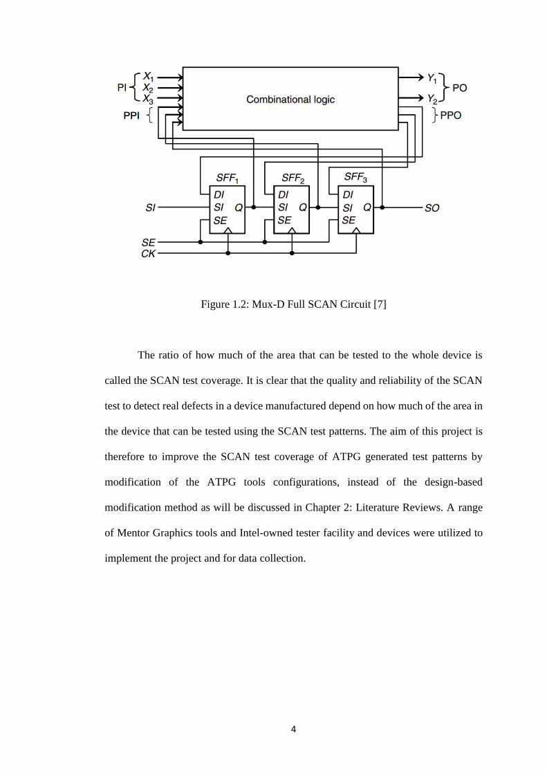
The scan cells are organized into shift registers and connected together to form
scan chains as shown in Figure1.2. Utilizing these scan chains, test patterns are
generated using Automatic Test Pattern Generation (ATPG) method to test the
combinational logic inside the design model. The control element is obtained by
setting a specific value at a specific node. Whereas, the observation element is obtained
by propagating the result so it can be measured.
4
Figure 1.2: Mux-D Full SCAN Circuit [7]
The ratio of how much of the area that can be tested to the whole device is
called the SCAN test coverage. It is clear that the quality and reliability of the SCAN
test to detect real defects in a device manufactured depend on how much of the area in
the device that can be tested using the SCAN test patterns. The aim of this project is
therefore to improve the SCAN test coverage of ATPG generated test patterns by
modification of the ATPG tools configurations, instead of the design-based
modification method as will be discussed in Chapter 2: Literature Reviews. A range
of Mentor Graphics tools and Intel-owned tester facility and devices were utilized to
implement the project and for data collection.
5
1.2 Problem Statements
Today’s demands for high quality semiconductor devices especially in the
automotive industry are extremely challenging [8]. The most important factor for this
demand is the reliability of the devices in its application. Higher performance of the
integrated circuits comes with the challenges of designing more complex and denser
digital circuits, making chips more prone to defects [9]. In modern deep submicron
technologies, systematic defects are becoming more common than random defects in
a device manufactured [10].
In order to achieve low Defect per Million (DPM) in the semiconductor
fabrication, the device under test (DUT) need to be tested as thoroughly as possible.
There are many manufacturing tests available such as memory built-in-self-test,
functional test and SCAN test. In terms of SCAN test, the thoroughness of the device
being tested depends on the coverage number of the test. A high test coverage is needed
in order to test as many logic cells as possible in the design.
The usual test coverage percentages required for a reliable stuck-at test is 95%
after excluding the untestable faults [11]. This number represents the full-chip
percentage that is being tested. However, there are some partitions in the design that
are having lower individual test coverage when the test patterns are generated for that
partitions. Patterns are generated per partition to ease the ATPG tool to evaluate the
faults and also to reduce run time for the pattern generation. In this project, the test
coverage is calculated based on partitions used, so a test coverage of less value can be
expected. In this case, the original partition-based test coverage was 85.64% which

6
was obtained based on an Intel chipset product design. In order for the product to be
tested as much as possible, and preventing defective devices to flow to customers, the
test coverage need to be improved.
For a Product Development Engineers (PDEs) working on the SCAN test
contents for devices validation, these partitions having lower initial test coverage are
posing a problem whereby, the total test coverage for the full-chip would accumulate
to be less than 95%. This problem, if not resolved, would be seen after the device has
been shipped to customers, during the post Failure Analysis stage, where it would be
reported that the said partitions are the ones causing the high fallout or escapee devices.
For PDEs validating the design provided during pre-silicon validation, they can
improve the test coverage by analyzing the design in what is called a low coverage
analysis and feedback to the design team to make the proper adjustment to improve
the test coverage. This is usually a time consuming approach. Also, a high level of
expertise is needed in order to root-cause the low coverage issue in a complex design.
Design-based approaches to improve the test coverage via modifying the
design for example, modified scan cell, scan cell reordering and extra signal addition
are available and discussed in Chapter 2. Electronic Design Automation (EDA) entities
such as Synopsys and Mentor Graphics who claim that they are getting significant
revenue in their verification segments [12] are providing tools that could help to tackle
this issue in a different way.
As a more feasible solution for PDEs to improve test coverage in a shorter time,
the modification on the ATPG tools configuration is proposed to improve the test

7
coverage instead of the design-based approach. A higher test coverage of test patterns
can be obtained if proper configurations are done on the ATPG tools during pattern
generation. A thorough understanding of what the configurations do is needed in order
to generate a reliable test patterns with a high test coverage. Although, it should be
noted, by modifying the ATPG tool’s configuration does not mean that the circuit
design would be changed. The modification would alter the way the ATPG tool learn
about the circuit and providing higher effort to generate test patterns with higher test
coverage. Thus, the improvement in test coverage would not be as much as the design-
based approach but it would save a lot of time in the test content generation stage
because fix in the circuit design is not needed.
1.3 Project Objectives
To improve the coverage of a SCAN test by proposing a few modification on
the switches combination available in ATPG tool from the current default flow.
To implement the experimental switch combinations in a test pattern
generation and collect the SCAN coverage reported by the ATPG tool for the
generated patterns.
To make a comparison on the coverage readings for the various switch
combinations and to provide analytical comments regarding the difference in
the test coverage obtained.

8
1.4 Project Scope
This project mainly covers the SCAN test coverage improvement for one
integrated circuit design. The coverage improvement method proposed in this project
is based on ATPG tools configurations and not on design-based methods. The resultant
test coverage generated based on the few experiments planned were compared and the
pattern generated from the most comprehensible experiments based on the comparison
and analysis were converted to tester pattern format (.pobj) and tested on a real device
to see the behavior. No further debug was made based on the tester result obtained.
1.5 Project Contribution
Today’s demand for high quality semiconductor devices manufacturing has led
to the importance of testing the devices as much as possible. This translates to the
needs for a high test coverage in test patterns to be used for the test and validation of
the devices. In this project, an improvement in the SCAN test coverage by ATPG tools
configuration was studied and presented. This method proposed instead of the design-
based approach as will be discussed in Chapter 2 would save a lot of labor resources
and time especially for Product Development Engineers working specifically on the
test pattern generation with no exposure to the design methodology of a device.
Although, the test coverage improvement by using this method is not as much as the
design-based approaches, the amount of time saved compared to the design-based
approaches made this method suffice.

9
1.6 Thesis Outline
This thesis was organized into five chapters including this Chapter 1:
Introduction. The following chapters are summarized and structured as below:
At the beginning of Chapter 2, the theories and flow of SCAN test are discussed
including the fault models and SCAN test coverage theories. Then, a discussion on the
Design for Test (DFT) flow and product development flow are briefly done.
Afterwards, previous works and papers related to the SCAN test coverage
improvement are discussed also in this chapter. Lastly, the Tessent ATPG tool’s
environment is briefly discussed.
Chapter 3 presents methodology of this project from designing the experiments
for the different configurations of the ATPG tool, test coverage determination and
comparison, to the validation of the test patterns generated on a real device. The details
of the experimental setup flow and tools applied are discussed and elaborated in this
chapter.
Chapter 4 presents the results obtained from the experiments designed in
Chapter 3. Comparison on the different data obtained are also made. The results are
tabulated and analyzed in detail in this chapter.
Chapter 5 outlines the conclusions that can be made based on this project’s
findings and the prospects of future works in this field of research.
10
CHAPTER 2
LITERATURE REVIEW
2.1 Introduction
The main goal of this project is to improve test coverage of SCAN test patterns
to reduce the defect per million (DPM) in silicon manufacturing. Previous proposed
theories and researches that relate to this goal were discussed in this chapter. The
following sections are separated into two parts, first, discussions on the relevant
theories related to this project were reviewed. Overview on the VLSI development
process and its testing essentials were first discussed. Then, automatic test equipment
(ATE) was reviewed for their components and special features. After that, a
methodology called design for test (DFT) which was used in this project was
discussed. This includes scan design and its operations. Various fault models for scan
test were also discussed along with the fault simulation process. Lastly, the scan test
pattern generation and scan test coverage calculation were discussed. These are the
basis of achieving the main objective of this project.
After knowing the relevant theories, in the second section, reviews on previous
design-based researches on scan coverage improvement were made. There are
basically five schemes that were reviewed in this section with various researches done
on them. The schemes reviewed were combination of different scan capture styles,
multiple scan enable signals, delay test scan flip-flop (DTSFF), dummy flip-flops and

11
additional multiplexer as well as scan chain reordering and dummy latches. Critical
reviews on various research papers related to these five schemes were done in this
section. The limitations for those researches were also discussed in this section. The
reviewed papers coming from design-based researches, served as a motivation on the
importance of having a high test coverage in the manufacturing world. The limitations
on these researches were addressed and a workaround was proposed with this project.
2.2 Relevant Theories
2.2.1 VLSI Development Process
The improvement in integrated circuit (IC) manufacturing and the existence of
high quality microchips has resulted in the need for better testing for these devices.
Following the Moore’s Law [13] the scale of integrated circuits has doubled every 18
months to the very-large-scale integration (VLSI) devices existing today. This
consequently led to the reduction in the feature size of the transistors and
interconnecting wires from tens of microns to the current technology node of less than
tens of nanometers. The reduction in dimension has resulted in increased clock speeds
and operating frequency of the IC from the first microprocessor running at the speed
of 108 kHz, to several gigahertz currently.
The dimension reduction also has resulted in an increased in the probability of
a manufacturing defect in the IC that can result in a faulty chip. A very small defect
existing in nanometer devices can affect the behavior of the devices and result in faulty

12
transistors. Defects existing during the manufacturing process are unavoidable, and
due to this fact, some number of ICs are expected to be faulty and the manufacturer
need to absorb that small amount of losses. Therefore, proper testing is required to
ensure that faulty devices doesn’t pass the test and escape to the customers. It is also
necessary to test the devices at various stages of the devices’ manufacturing cycle.
There is a general agreement that mentions the cost of detecting a defective
device increases by certain amount of magnitude as the manufacturing cycle is moved
to the later stage, from device level to board level, to the system level and finally to
the system operation in the customers’ environments. Testing devices also helps in
improving production yield by analyzing the cause of defects when faults are detected.
In some cases, repair on the devices are done to counter the faults detected. Hence,
testing is important to designers, product engineers, test engineers, managers,
manufacturers, and end-users [14].
2.2.2 VLSI Testing
Testing consists of applying a set of input stimuli to the circuit under test (CUT)
and analyzing the resulting output responses as illustrated in Figure 2.1. Production
testing applies test patterns to exercise devices for defect detection. Defects are
physical problems that occur in silicon due to the fabrication process. Defects may
cause the silicon to perform differently from the design [7]. Defect free devices are
candidates for shipping to customers. The devices that fail the test will be considered
as rejected devices. Too much of the rejected devices will lead to lower production
yield. Sometimes devices with a defect will pass all applied tests. These are known as
13
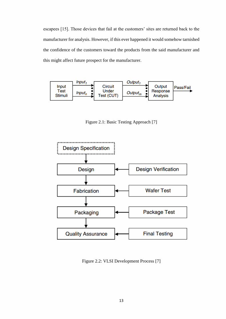
escapees [15]. Those devices that fail at the customers’ sites are returned back to the
manufacturer for analysis. However, if this ever happened it would somehow tarnished
the confidence of the customers toward the products from the said manufacturer and
this might affect future prospect for the manufacturer.
Figure 2.1: Basic Testing Approach [7]
Figure 2.2: VLSI Development Process [7]
14
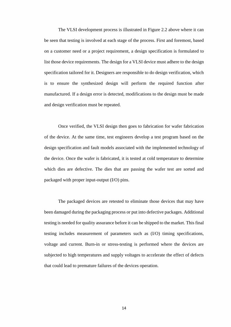
The VLSI development process is illustrated in Figure 2.2 above where it can
be seen that testing is involved at each stage of the process. First and foremost, based
on a customer need or a project requirement, a design specification is formulated to
list those device requirements. The design for a VLSI device must adhere to the design
specification tailored for it. Designers are responsible to do design verification, which
is to ensure the synthesized design will perform the required function after
manufactured. If a design error is detected, modifications to the design must be made
and design verification must be repeated.
Once verified, the VLSI design then goes to fabrication for wafer fabrication
of the device. At the same time, test engineers develop a test program based on the
design specification and fault models associated with the implemented technology of
the device. Once the wafer is fabricated, it is tested at cold temperature to determine
which dies are defective. The dies that are passing the wafer test are sorted and
packaged with proper input-output (I/O) pins.
The packaged devices are retested to eliminate those devices that may have
been damaged during the packaging process or put into defective packages. Additional
testing is needed for quality assurance before it can be shipped to the market. This final
testing includes measurement of parameters such as (I/O) timing specifications,
voltage and current. Burn-in or stress-testing is performed where the devices are
subjected to high temperatures and supply voltages to accelerate the effect of defects
that could lead to premature failures of the devices operation.

15
2.2.3 Yield and Reject Rate
It is most certain that some percentage of the manufactured ICs is expected to
be faulty due to manufacturing process [7]. The yield of a manufacturing process is
defined as the percentage of acceptable parts among all parts that are fabricated as
shown in (Eqn. 2-1):
Yield (%) = 𝑁𝑢𝑚𝑏𝑒𝑟 𝑜𝑓 𝑎𝑐𝑐𝑒𝑝𝑡𝑎𝑏𝑙𝑒 𝑝𝑎𝑟𝑡𝑠
𝑇𝑜𝑡𝑎𝑙 𝑛𝑢𝑚𝑏𝑒𝑟 𝑜𝑓 𝑝𝑎𝑟𝑡𝑠 𝑓𝑎𝑏𝑟𝑖𝑐𝑎𝑡𝑒𝑑 (Eqn. 2-1)
There are two types of yield loss:
1) Catastrophic – due to random defects.
2) Parametric – due to process variations.
Automation and improvements in a VLSI fabrication process drastically reduce
the particle density that can result in random defects over time. Consequently,
parametric yield loss becomes dominant in current VLSI technology. When ICs are
tested, two undesirable outcomes may occur:
1) A faulty device may appear to be passing the test.
2) A good device may appear to be failing the test.
These are often due to a poorly designed test or the lack of Design for testability
(DFT). For the first case, even if all parts are passing the test, some faulty devices will
still be found in the field electronic systems. When these faulty devices are returned to
the IC manufacturer, they undergo failure mode analysis for possible improvements to
the VLSI development and manufacturing processes. The ratio of field-rejected parts
to all parts passing quality assurance test is referred to as the reject rate or defect level
as shown in (Eqn. 2-2).

16
Reject Rate = 𝑁𝑢𝑚𝑏𝑒𝑟 𝑜𝑓 𝑓𝑎𝑢𝑙𝑡𝑦 𝑝𝑎𝑟𝑡𝑠 𝑝𝑎𝑠𝑠𝑖𝑛𝑔 𝑓𝑖𝑛𝑎𝑙 𝑡𝑒𝑠𝑡 (𝑟𝑒𝑡𝑢𝑟𝑛𝑒𝑑)
𝑡𝑜𝑡𝑎𝑙 𝑛𝑢𝑚𝑏𝑒𝑟 𝑜𝑓 𝑝𝑎𝑟𝑡𝑠 𝑝𝑎𝑠𝑠𝑖𝑛𝑔 𝑓𝑖𝑛𝑎𝑙 𝑡𝑒𝑠𝑡 (Eqn. 2-2)
The reject rate provides an indication of the overall quality of the VLSI testing
process [16]. Generally, a reject rate of 500 defects per million (DPM) may be
considered as acceptable, while 100 DPM or lower shows that the test is high in
quality.
2.2.4 Automatic Test Equipment (ATE)
Test application is the process of applying test vectors to the DUT and
analyzing the output responses. Test application is performed either by automatic test
equipment (ATE) or by the technologies inside the chip itself. ATE is an equipment
controlled by computer in the production testing of ICs both at the wafer level and in
packaged form. Utilizing ATE, test patterns are applied to the DUT and the output
responses are compared to the stored responses for a fault-free circuit. ATE has the
capability to perform diagnosis on the failure observed to identify the source of the
issue [7].
Without the introduction of ATE, testing would become a bottleneck to the
high-volume production of ICs due to the repetitive tasks needed to be performed
manually by technicians or lab operators. Automation made available by ATE had
tremendously contributed to the success of IC production today. Development of a
custom tester is usually for testing a particular product, whereas a general-purpose

17
ATE is often more flexible and enhances the productivity of high-volume
manufacturing of ICs.
From a VLSI development point of view, there has been a significant decrease
in the capital cost of manufacturing a transistor over the past decades. However as
more complex devices are delivered, the test cost are becoming an increasing portion
of the overall industry capital requirement per transistor. In the advancement and ever-
changing of VLSI testing, ATE costs should be kept under control too.
In this project, an ATE in the form of Advantest tester is used to apply the
coverage-improved test patterns generated to observe the output responses on a real
device. Before the first silicon is made available, the patterns to be tested on the ATE
should be verified by simulating the patterns and the design model. ATPG tools allow
to dump a test bench to do the verification on the generated scan patterns. A timing
simulation with delay data for all lines and logic gates should be performed to take
into account not only logical behavior but also timing of the design. The scan patterns
generated from the ATPG should be converted to a format such as Standard Tester
Interface Language (STIL) which can be easily converted into test vectors for the ATE
usage.
2.2.5 Design for Test (DFT)
During the early stages of IC production history, design and test of the device
were regarded as separate functions, performed by separate and unrelated group of
engineers [7]. Design engineers were to design a circuit based on the required

18
functionality based on the design specification without giving any thought on how the
manufactured device was to be tested. After the design was handed to test engineers,
efficient test was to be constructed to screen out the parts that may contain
manufacturing defects and ship the rest to customers. Based on customer returns,
measurements are calculated as defects per million (DPM) shipped, as a final test core
of the quality of the test.
However as circuit complexity increased, a common approach to test these
devices during the 1980s relied heavily on fault simulation to measure the fault
coverage of the supplied functional patterns in the CUT [7]. If the supplied patterns
did not reach the target fault coverage goal, additional functional patterns were added.
These functional patterns navigate through the long sequential depths of the design,
with the goal of exercising all the internal states and detecting all possible
manufacturing defects. Unfortunately, this approach typically failed to improve the
CUT’s fault coverage beyond 80% and as a result, the quality of the products shipped
suffered.
Gradually, the fine line between design and test was blurred down and led to
the development and deployment of design for test (DFT) engineering in the industry.
The first challenge facing DFT engineers was to find simpler ways of exercising all
internal states of a design and reaching the target fault coverage. Various methods were
proposed in 1970s and 1980s to aid in the circuit’s testability or to increase the circuit’s
controllability and observability [17] [18].

19
For combinational circuits, generating test patterns within a reasonable amount
of time was not difficult with many innovative ATPG algorithms already existed.
However, for sequential circuits, due to numerous internal states that are difficult to
set and check from external pins, automatically generating test patterns did not work
so well. Hence, structured DFT approaches were developed whereby, direct external
access is provided in the circuit for storage elements. The reconfigured storage
elements with direct external access are commonly known as scan cells. As a result of
this capability, testing the sequential circuit is transformed into a problem of testing
the combinational circuit which already has many existing solutions.
2.2.6 Scan Design and Scan Design Rules Overview
Scan design is currently the most popular structured DFT approach. The way
it is implemented is by connecting the scan cells of a design into multiple shift registers
called scan chains, to provide them with external access. Scan design achieved this by
replacing the flip-flops with scan cells, each having an additional port called scan input
(SI) and a shared port called scan output (SO). The scan chains are created by
connecting the SO port of a scan cell to the SI port of another scan cell. In order for a
scan design test to achieve the desired DPM goal, specific circuit structure and design
practices that can affect fault coverage of the circuit must be met. These requirements
which are known as scan design rules must be adhered by DFT engineers, whereby
any scan design rule violation must be fixed. The test patterns generated for the scan
design must be converted to test programs for test engineers to perform manufacturing
testing on the real ICs using an ATE.
20
2.2.7 Scan Mode of Operations
The structured DFT approach attempts to improve the overall testability of a
circuit with a test-oriented design methodology [19] [20]. This methodological and
systematic approach produces more predictable results. Scan design, the most widely
used structured DFT approach, attempts to improve testability by providing the
controllability and observability of storage elements in a sequential design. This
includes converting the sequential design into a scan design with three modes of
operation: normal mode, shift mode and capture mode.
In normal mode, all test signals are not exercised, and the circuit operates in
the functional configuration. Whereas, in shift and capture modes, a test mode (TM)
signal is often used to exercise all test-related signals to simplify the test, debug,
diagnosis tasks, improve fault coverage and guarantee the safe operation of the circuit
under test. These circuit modes and operations consist of different test signals and test
clocks.
Referring to Figure 2.3, this sequential circuit contains combinational logic and
three normal D flip-flops. Assume that a stuck-at fault f in the combinational logic
requires the primary input X3, flip-flops FF2 and FF3 to be set to 0, 1 and 0 respectively,
to capture the fault effect into FF1. The values stored in FF2 and FF3 are not directly
controllable from the primary inputs, thus require a long sequence of operations to set
their values. Same goes when the fault effect observation is needed in F1, a long
propagation is needed for the value to propagate to a primary output. Obviously, while
the output response of a scan test pattern is shifted out of a scan chain, the scan chain

21
can be shifted in with the scan input data of the next test pattern to save overall test
time. The resultant test time for a scan test depends mostly on the number of scan test
patterns used, the size of the longest scan chain and the shift frequency.
Figure 2.3: Testing a Normal Sequential Circuit for Fault, f [7]
With scan design, external access to the flip-flops are made available for easier
controllability and observability. The flip-flops are converted into scan cells and
stitched together to form one or more shift registers called scan chains. Test stimuli
can now be shifted in and out of the scan cells with significantly more predictable and
lower clock cycles needed. Hence, the task of detecting fault f can be done by:
1) Shifting in the desired stimuli in shift mode.
2) Switching to capture mode and applying one clock pulse to capture the fault
effect into FF1.
22
3) Switching back to shift mode and shift out the test responses stored in FF1, FF2
and FF3 for comparison with the expected response.
2.2.8 Mux-D Scan Cell
The most widely used scan cell design is the Mux-D scan flip-flop as shown in
Figure 1.1. This scan cell composed of a D flip-flop and a multiplexer. Its basic
function is to pass a logic value from its input to its output when a clock signal is
applied. The multiplexer uses a scan enable (SE) signal to select between the data input
(DI) and the scan input (SI). In normal/capture mode, SE is set to 0 to get input from
DI when a rising clock edge is applied. In shift mode, SE is set to 1 to get new data
from SI while the content of the D flip-flop is shifted out.
Major advantages of using mux-D scan cells are their compatibility to modern
designs using single-clock D flip-flops as storage elements and the comprehensive
support provided by existing design automation tools which will be used in this project.
Also, the additional area overhead is small and there are no or very relaxed timing
constraints on the scan enable signal. The disadvantage however, each mux-D scan
cell adds a multiplexer delay to the functional path, therefore it might reduce the
maximum frequency for functional operation.
2.2.9 Scan Design Rules
In order to integrate scan into a design, the design must adhere to a set of scan
design rules [21]. Furthermore, a set of design style must be avoided to prevent low
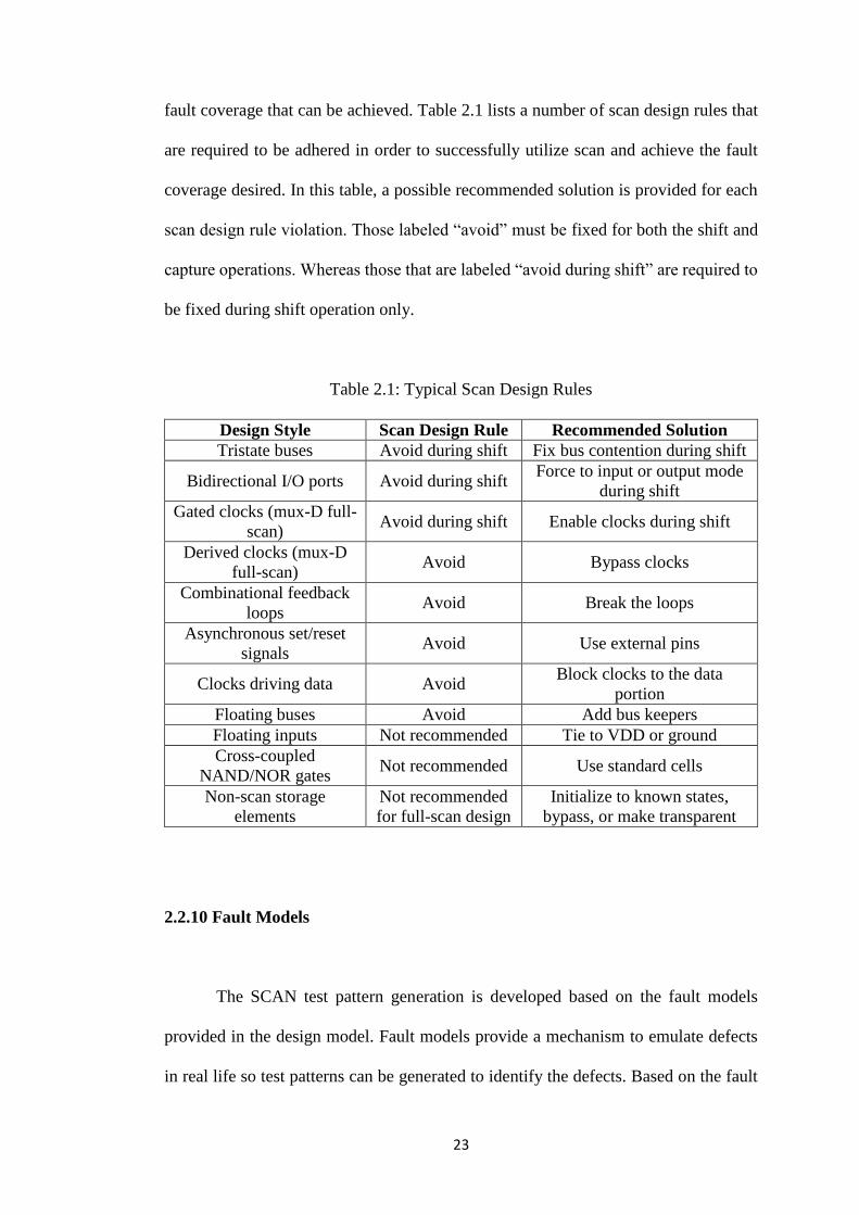
23
fault coverage that can be achieved. Table 2.1 lists a number of scan design rules that
are required to be adhered in order to successfully utilize scan and achieve the fault
coverage desired. In this table, a possible recommended solution is provided for each
scan design rule violation. Those labeled “avoid” must be fixed for both the shift and
capture operations. Whereas those that are labeled “avoid during shift” are required to
be fixed during shift operation only.
Table 2.1: Typical Scan Design Rules
Design Style Scan Design Rule Recommended Solution
Tristate buses Avoid during shift Fix bus contention during shift
Bidirectional I/O ports Avoid during shift Force to input or output mode
during shift
Gated clocks (mux-D full-
scan) Avoid during shift Enable clocks during shift
Derived clocks (mux-D
full-scan) Avoid Bypass clocks
Combinational feedback
loops Avoid Break the loops
Asynchronous set/reset
signals Avoid Use external pins
Clocks driving data Avoid Block clocks to the data
portion
Floating buses Avoid Add bus keepers
Floating inputs Not recommended Tie to VDD or ground
Cross-coupled
NAND/NOR gates Not recommended Use standard cells
Non-scan storage
elements
Not recommended
for full-scan design
Initialize to known states,
bypass, or make transparent
2.2.10 Fault Models
The SCAN test pattern generation is developed based on the fault models
provided in the design model. Fault models provide a mechanism to emulate defects
in real life so test patterns can be generated to identify the defects. Based on the fault

24
model, the expected good behavior is determined first hand by the ATPG tool. A fault
is detected when there is an observed difference between good behavior and faulty
behavior. The most common fault model is a stuck-at fault model introduced in 1959
[22]. Stuck-at patterns detect a very large percentage of all faults. Another common
fault model, is the at-speed fault model which can be divided into transition and path
delay based. Besides that, there are also other fault models such as layout aware bridge
and user-defined (UDFM) fault models. Requirements for low Defect per Million
(DPM) of semiconductor devices typically drive the need for additional fault models.
2.2.11 Targeted Fault Models of Scan Tests
a) Single Stuck-At Fault (SSF) Model
The classical fault model of a scan test is the single stuck-at fault (SSF) model
introduced in 1959 [22]. In this model, only a single line is fault modeled to be stuck-
at 0 or stuck-at 1. Most people assume the SSF model as stuck-at fault model, which
is not precise since multiple stuck-at faults would mean a significantly larger set of
faults that can be hardly handled by automatic test pattern generation (ATPG)
algorithms. SSF model has the following properties:
- In a circuit design, the number of SSFs increases linearly with the number of
flip-flops.
- The ratio of the number of SSFs that can be detected by a given scan test, can
be the gauge for the quality of the scan test.
- For a highly efficient scan test patterns just focusing on a SSF model, coverage
of other faults and defects that exist in the circuit might not be that good [23]
and this can be improved, if the ATPG tool is configured to detect each SSF n-
times and not only with one pattern (n-detect SSF scan patterns) [24][25].