“socket signal integrity – impact from ic & board”
TRANSCRIPT

BiTS Workshop 2007 Archive
���������� Session 5
ARCHIVE 2007
PCB ADVANCEMENTS AND OPPORTUNITIES
“Socket Signal Integrity – Impact From IC & Board” James Zhou, Jiachun (Frank) Zhou Antares Advanced Test Technologies
“Minimizing Socket & Board Inductance Using a Novel De-Coupling Interposer”
Nicholas Langston, Sr., James Zhou, Hongjun Yao Antares Advanced Test Technologies
“Benchmarking Printed Circuit Board Fabrication Suppliers Using IPC PCQR2 Database”
Bill Mack Texas Instruments Inc.
COPYRIGHT NOTICE
The papers in this publication comprise the proceedings of the 2007 BiTS Workshop. They reflect the authors’ opinions and are reproduced as presented , without change. Their inclusion in this publication does not constitute an endorsement by the BiTS Workshop, the sponsors, BiTS Workshop LLC, or the
authors.
There is NO copyright protection claimed by this publication or the authors. However, each presentation is the work of the authors and their respective companies: as such, it is strongly suggested that any use
reflect proper acknowledgement to the appropriate source. Any questions regarding the use of any materials presented should be directed to the author/s or their companies.
All photographs in this archive are copyrighted by BiTS Workshop LLC. The BiTS logo and ‘Burn-in & Test Socket Workshop’ are trademarks of BiTS Workshop LLC.

20072007Session 5
March 11 - 14, 2007
Paper #1
1
PCB Advancements And Opportunities
1
Socket Signal Integrity –Impact from IC & Board
James Zhou, presenterJiachun Zhou (Frank)
Antares Advanced Test Technologies
March 11-14, 2007Hilton Phoenix East, Mesa Arizona
2
2
Outline
IntroductionQFN package + spring pin socket BGA package + spring pin socketLGA pad size vs. bandwidthSummary

20072007Session 5
March 11 - 14, 2007
Paper #1
2
PCB Advancements And Opportunities
3
3
Introduction• Package test system:IC package + Contactor/socket + Load board• Common practice to simulate SI performance
separately- attempt to derive the system performance from
individual sub-systems of loadboard, socket and package.
• In reality these components have EM coupling between each other. SI performance of each component is affected by other components.
• Analysis on system level coupling effects between components are presented.
Load board
PackageContactor/socket
4
Spring pin socket for QFN package

20072007Session 5
March 11 - 14, 2007
Paper #1
3
PCB Advancements And Opportunities
5
5
A Simple QFN Package Model
• Two signal paths formed by: - PCB pads- QFN pads- Bondwires- Signal pads on silicon
• Ground loop formed by:- PCB ground plane- 2x4 via array- QFN ground pad- Bondwires- Ground pads on silicon
Siliconsubstrate
Packageground
PCB groundvias
pads
6
6
QFN Package Performance
Insertion loss (IL): IL = 1dB @4.9GHzReturn loss (RL): RL = [email protected] (XT): XT = 30dB@1GHz
20072007Session 5
March 11 - 14, 2007
Paper #1
4
PCB Advancements And Opportunities
7
7
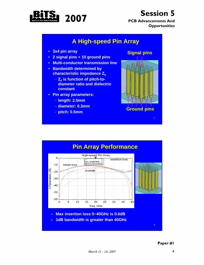
A High-speed Pin Array• 3x4 pin array • 2 signal pins + 10 ground pins • Multi-conductor transmission line• Bandwidth determined by
characteristic impedance Z0
- Z0 is function of pitch-to-diameter ratio and dielectric constant
• Pin array parameters: - length: 2.5mm- diameter: 0.3mm- pitch: 0.5mm
Signal pins
Ground pins
8
8
Pin Array Performance
• Max insertion loss 0~40GHz is 0.6dB• 1dB bandwidth is greater than 40GHz
20072007Session 5
March 11 - 14, 2007
Paper #1
5
PCB Advancements And Opportunities
9
9
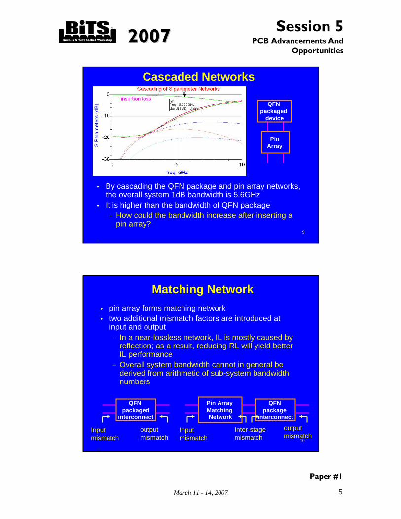
Cascaded Networks
• By cascading the QFN package and pin array networks, the overall system 1dB bandwidth is 5.6GHz
• It is higher than the bandwidth of QFN package - How could the bandwidth increase after inserting a
pin array?
Pin Array
QFN packaged
device
10
10
Matching Network• pin array forms matching network• two additional mismatch factors are introduced at
input and output- In a near-lossless network, IL is mostly caused by
reflection; as a result, reducing RL will yield better IL performance
- Overall system bandwidth cannot in general be derived from arithmetic of sub-system bandwidth numbers
Pin Array Matching Network
QFN package
interconnect
QFN packaged
interconnect
Input mismatch
output mismatch
Input mismatch
output mismatch
Inter-stagemismatch

20072007Session 5
March 11 - 14, 2007
Paper #1
6
PCB Advancements And Opportunities
11
11
3D Full-wave EM Analysis
• 3D full-wave EM analysis (HFSS) of entire system• 1dB bandwidth is 2.3GHz, less than half of QFN
package bandwidth of 4.9GHz• Bandwidth significantly lower than cascading
network bandwidth of 5.6GHz. • What has gone wrong?
12
12
A Low-speed Pin Array
• 1dB bandwidth = 7.3GHz, significantly lower than the high speed pin array- Pin array parameters: length=2.5mm;
diameter=0.4mm; pitch=0.5mm
20072007Session 5
March 11 - 14, 2007
Paper #1
7
PCB Advancements And Opportunities
13
13
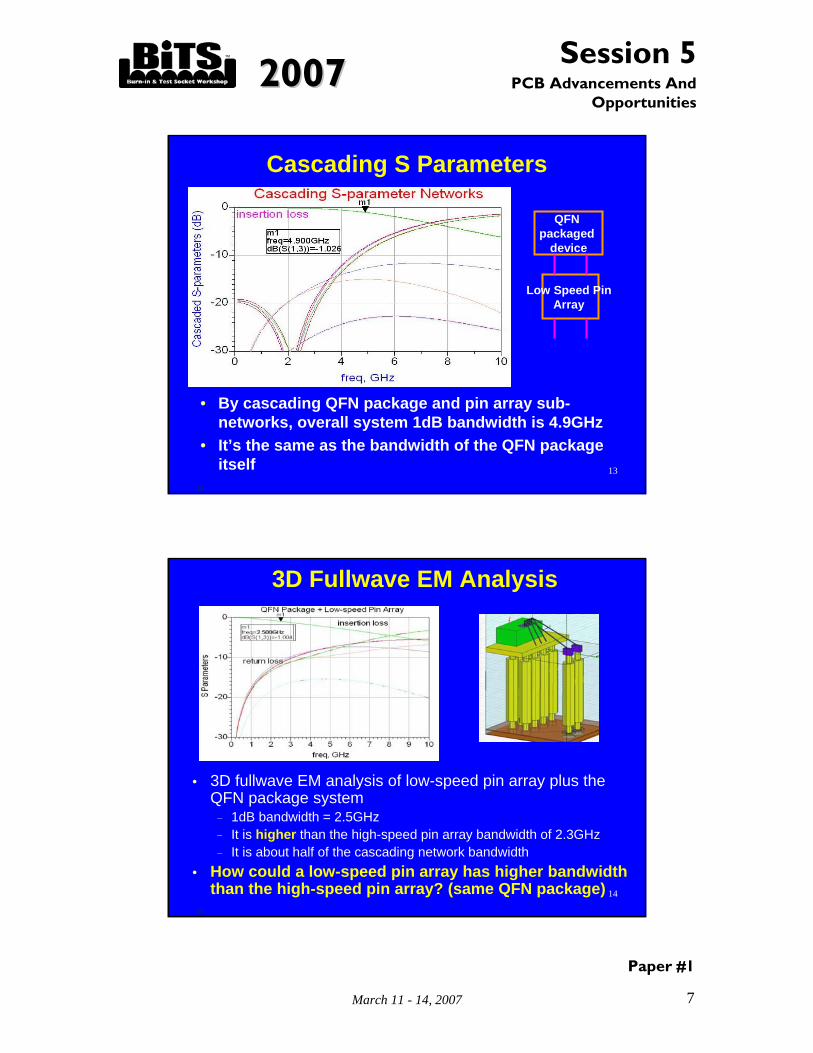
Cascading S Parameters
• By cascading QFN package and pin array sub-networks, overall system 1dB bandwidth is 4.9GHz
• It’s the same as the bandwidth of the QFN package itself
Low Speed Pin Array
QFN packaged
device
14
14
3D Fullwave EM Analysis
• 3D fullwave EM analysis of low-speed pin array plus the QFN package system- 1dB bandwidth = 2.5GHz- It is higher than the high-speed pin array bandwidth of 2.3GHz - It is about half of the cascading network bandwidth
• How could a low-speed pin array has higher bandwidth than the high-speed pin array? (same QFN package)

20072007Session 5
March 11 - 14, 2007
Paper #1
8
PCB Advancements And Opportunities
15
15
Observations• QFN package itself has a 1dB bandwidth of 4.9GHz• cascading S-parameter networks: the overall
system bandwidth is equal to or higher than the bandwidth of the QFN package
• 3D fullwave EM analysis: the overall system bandwidth is significantly lower than the QFN package
• Low-speed pin has slightly better performance than the high-speed pin in the overall system (WHY?)
• 3D fullwave analysis reveals additional source of insertion loss from radiation- Pins surrounded by all ground pins has much
less radiation
16
16
Discussion – Cascaded Networks• Cascaded network technique is often
used in the calculation of overall system performance from individual sub-systems of PCB, socket and package
• In network analysis, the input/output ports are assumed to be terminated by infinitely long transmission lines
Pin Array Matching Network
QFN package
interconnect
Matched ports
Matched ports
Invisible transition not formed yet

20072007Session 5
March 11 - 14, 2007
Paper #1
9
PCB Advancements And Opportunities
17
17
Cascaded Networks (cont.)• when two networks of disparate interface
geometries are cascaded, this important termination condition is violated
• An extra “invisible transitional network” has been created in the system, which characteristics are totally unaccounted for- Higher order modes exist in the vicinity of the
transition
Pin Array Matching Network
QFN package
interconnect
Invisible transition formed
Higher order modes
18
18
Discontinuity and Mismatch• By separating a system at its discontinuity points,
potentially large errors can be introduced due to impedance mismatch and higher order mode
• Discontinuities causes impedance mismatch; higher order modes EM fields exist in its vicinity
• when a reference plane is set up at these locations, the field patterns are greatly disturbed by the reference planes and port structure, resulting in potentially large errors
When system boundary is setup at discontinuity transitional locations, large errors can occur
Ref plane

20072007Session 5
March 11 - 14, 2007
Paper #1
10
PCB Advancements And Opportunities
19
19
The Golden Rule• When using “reference planes” to break a system into
sub-systems, the planes must be located at uniform transmission lines with fair distance on both sides of the plane away from any discontinuity.
• The interface between socket and package is NOT in the middle of a uniform transmission line; in fact it is one of the most significant discontinuity points in the system
Uniform transmission line across sub-network boundary
Ref plane
20
20
Socket Discontinuities
• Two biggest discontinuities in a socket system:- PCB to socket transition- Socket to package transition
• Spring pins also have discontinuities :- Change of diameter- From plunger to shell- From shell/plunger to pin tips
• By setting up input/output ports at these discontinuity locations, large errors usually occur
Socket to package transition
PCB to socket transition
Spring pin discontinuities

20072007Session 5
March 11 - 14, 2007
Paper #1
11
PCB Advancements And Opportunities
21
21
Port Setup
• To satisfy the fundamental requirements of port (reference plane) setup:- use microstrip or coplanar
waveguide (CPW) transmission lines
- setup the ports at fair distance away from any discontinuities of pad, via, dielectric boundary
22
22
Port Setup – long pins• For longer pins, reference
planes can be setup at mid-section of pins- Satisfy uniform
transmission line requirement
- Electrical boundaries do not necessarily follow natural mechanical boundaries
- Think out of the “box” and beyond the normal “boundaries”
package
PCB
Ref plane
pins

20072007Session 5
March 11 - 14, 2007
Paper #1
12
PCB Advancements And Opportunities
23
23
Board + Socket + Package
• In order to obtain accurate results on overall system bandwidth, it is highly desirable to analyze the entire system of load board + socket + package
• The input/output ports can be set up at locations of loadboard/package PCB traces, which are good uniform transmission lines
• This approach will guarantee the proper set up of the problem
Main board
PackageContactor/socket
24
Spring pin socket for BGA package

20072007Session 5
March 11 - 14, 2007
Paper #1
13
PCB Advancements And Opportunities
25
25
BGA Package Model
• 1dB bandwidth = 3.7GHz• Usable frequency up to 10GHz
signalspowerground
Signal layer
Ground layer
Power layer
26
26
BGA Package + High-speed Pins
• Using 40GHz high-speed pins with BGA package:- 1dB bandwidth = 1.7GHz- Less than half of BGA package bandwidth
20072007Session 5
March 11 - 14, 2007
Paper #1
14
PCB Advancements And Opportunities
27
27
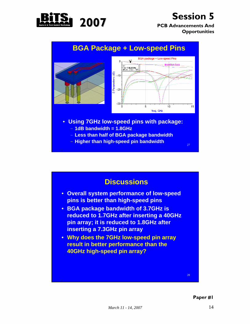
BGA Package + Low-speed Pins
• Using 7GHz low-speed pins with package:- 1dB bandwidth = 1.8GHz- Less than half of BGA package bandwidth- Higher than high-speed pin bandwidth
28
28
Discussions• Overall system performance of low-speed
pins is better than high-speed pins• BGA package bandwidth of 3.7GHz is
reduced to 1.7GHz after inserting a 40GHz pin array; it is reduced to 1.8GHz after inserting a 7.3GHz pin array
• Why does the 7GHz low-speed pin array result in better performance than the 40GHz high-speed pin array?

20072007Session 5
March 11 - 14, 2007
Paper #1
15
PCB Advancements And Opportunities
29
29
Discussions• Bandwidth of “package+socket” system is
not directly related to the individual sub-system bandwidth
• 3D EM effects must be simulated in one system
• Discontinuities between socket and package can only be accurately modeled in 3D full-wave analysis
• Radiation effects• Changing pitch will completely change
socket characteristic
30
LGA Pad Size vs. Bandwidth

20072007Session 5
March 11 - 14, 2007
Paper #1
16
PCB Advancements And Opportunities
31
31
LGA Pad sizes vs. IL
• Pin array: 2 signals, 10 grounds• Pad size sweep values: 0.3/0.5/0.7/0.9mm• 1dB bandwidth: 4.35/4.25/3.85/3.35 GHz
32
32
Discussion
• Very large pads are often used in LGA package for mechanical alignment tolerances
• These large pads have adverse effects on system bandwidth
• Large discontinuities and impedance mismatch exist at socket-to-package transition
• Degradation of IL cannot be easily overcome by spring pin design

20072007Session 5
March 11 - 14, 2007
Paper #1
17
PCB Advancements And Opportunities
33
33
SummaryThe discontinuities at PCB-to-socket and socket-to-package transitions must be evaluated as an integrated part of the systemCascaded network approach may result in large errors if these discontinuities are not modeled properlySocket SI performance is NOT just determined by the socket itself; it is dependent on the package and PCB designTo ensure best accuracy, model the PCB+socket+package as an integrated system using 3D full-wave EM tools
34
34
About Authors
James Zhou, Senior Technical StaffAntares ATT
1150 North Fiesta Blvd., Gilbert, AZ 85233Ph: (480)682-6200
Jiachun Zhou (Frank), PhDPD Eng Manager, Antares ATT
1150 North Fiesta Blvd., Gilbert, AZ 85233 Ph: (480)682-6225
20072007Session 5
March 11 - 14, 2007
Paper #2
1
PCB Advancements And Opportunities
2007 Burn-in and Test Socket WorkshopMarch 11 - 14, 2007
Nick LangstonJames Zhou, Hongjun Yao
Minimizing Socket & Board Inductance using a Novel
decoupling Interposer
2BiTS 2007
• It is better to uncover a little than to cover a lot.
• Eric Bogatin , SI Artisan» www.bethesignal.com

20072007Session 5
March 11 - 14, 2007
Paper #2
2
PCB Advancements And Opportunities
3BiTS 2007
Performance Limiting Noise
• Power ground voltage droop (Rail Collapse)
• Simultaneous Switching Noise (SSN –Ground Bounce)
• PDS Components• Board – Socket – DUT package – decoupling
components
4BiTS 2007
Hi Speed DUT PWR Del. Sys
Zt
Zm
IV
Z= V/I
ZFreq
PDS has to distribute the power to the chipHas to keep the ripple (noise) to spec ~ 5%Can not droop all the way to the BW of DUT

20072007Session 5
March 11 - 14, 2007
Paper #2
3
PCB Advancements And Opportunities
5BiTS 2007
Schematic of PDS with simple lumped models
Via-pogo
ElectrolyticBulk Capacitors
Inter-plane CapacitanceVoltage
RegulatorModule/Pwr Supplies
On-dieCapacitor Package Caps
VCC plane
Return plane
VCC Return
High Frequency Ceramic Decoupling Capacitors
BypassCapacitors Decaps
Lpcb
Lpkg Rpkg
CablePogo i/f
Low Freq Lo Z Mid Frequency Lo Z Hi Frequency Lo Z
6BiTS 2007
Powersupply
Powersupply
Load
Load
Cbypass
CbypassL dec
Cdec
Are Bypass and Decoupling the same?

20072007Session 5
March 11 - 14, 2007
Paper #2
4
PCB Advancements And Opportunities
7BiTS 2007
Basic PDS Design StrategyDetermine required PDS impedance
Z = ∆V/∆ I
Determine the frequency for the PDS aloneFpds = Z/ 2πL pds
Bypass C = 1/ 2πFpdsZ
Determine how much L we can handle at FmaxL = Z Tr/π
8BiTS 2007
Reviewing SSO/SSN/Ground Bounce
S1ATE DRIVER
LOSSY
LOAD BOARD
L2
LOSSYVIA
L7
SOCKET
VCC
boardVIA
DUT
BYPASS
L8
Decap
S1ATE DRIVER
Test Cell Schematic
SLM

20072007Session 5
March 11 - 14, 2007
Paper #2
5
PCB Advancements And Opportunities
9BiTS 2007
Loop I
Vgb = n x LnetVs Tr x Zo
3 nets, 5nH, 0.5ns Tr, 50 ohms 60% Vgb!
10BiTS 2007
Inductance is like Kryptonite!
• For Digital Designers of high speed test cells,
• Inductance is the bane of good designs
Capacitance is like Free Beer!

20072007Session 5
March 11 - 14, 2007
Paper #2
6
PCB Advancements And Opportunities
11BiTS 2007
Simulation of the impact of Bypassing
• 8 layer FR4 board; 0.635mm dielectric•5 .01uF caps on bottom of the board•1 power via; .25mm dia.; 0.5mm antipad
• Chip mounted directly to the board• Chip in a socket mounted to the board• Chip in a socket with the .01uF caps
12BiTS 2007
Load Configuration•10 ohm resitive load to draw 100ma
•from 1v supply•0.1nF on chip bypass on each power pin•Load is turned on at 5ns,
• the Tr is 200ps
20072007Session 5
March 11 - 14, 2007
Paper #2
7
PCB Advancements And Opportunities
13BiTS 2007
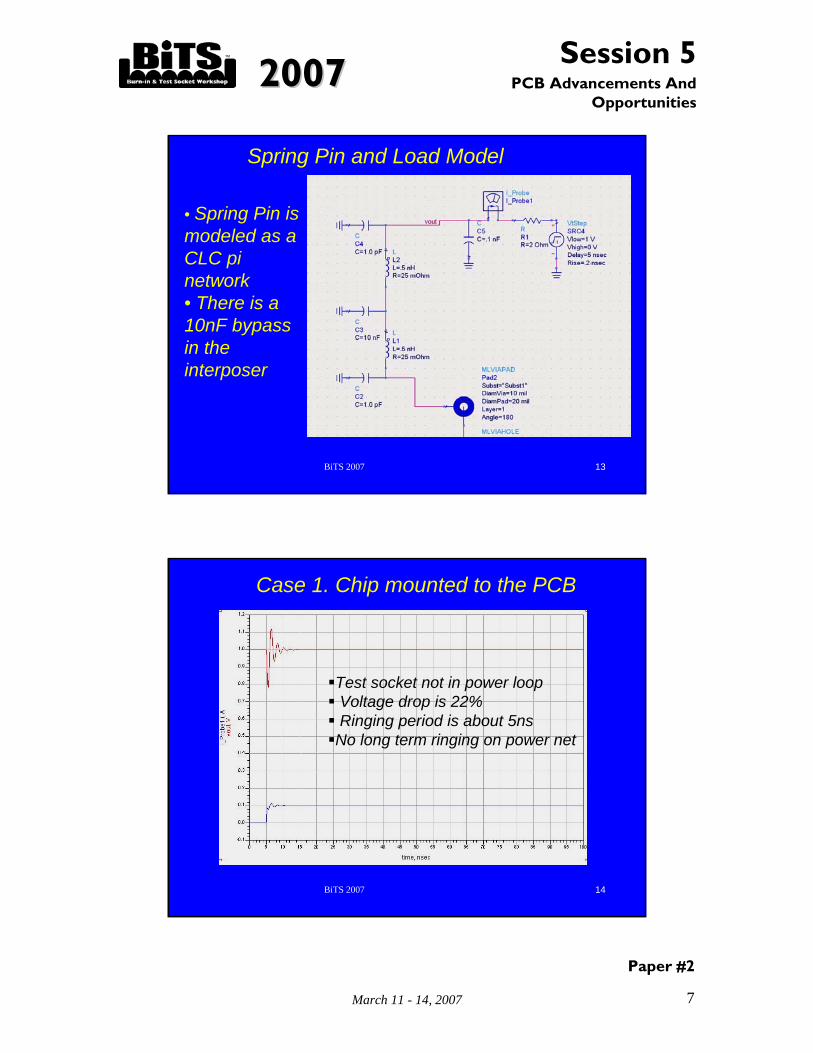
Spring Pin and Load Model
• Spring Pin is modeled as a CLC pi network• There is a 10nF bypass in the interposer
14BiTS 2007
Case 1. Chip mounted to the PCB
Test socket not in power loopVoltage drop is 22%Ringing period is about 5ns
No long term ringing on power net

20072007Session 5
March 11 - 14, 2007
Paper #2
8
PCB Advancements And Opportunities
15BiTS 2007
•Test socket in power loop without any bypass capacitor• Voltage drop is 31%• Ringing period is 7ns• No long term ringing
Case II: Using Socket with no bypass
16BiTS 2007
Case III: Contactor with bypass interposer
•Test socket in power loop •10nF interposer in skt
•Voltage drop is 18%•Ringing period is ~7ns•Ringing is longer term

20072007Session 5
March 11 - 14, 2007
Paper #2
9
PCB Advancements And Opportunities
17BiTS 2007
• 1nH test contactor increases the power drop from 22% to 31%
• 10nF bypass cap reduces the power drop to 18%
• The built-in bypass cap and the spring pin inductance causes some long term ringing on the power net..
Observations
18BiTS 2007
Interposer Position

20072007Session 5
March 11 - 14, 2007
Paper #2
10
PCB Advancements And Opportunities
19BiTS 2007
Decoupling Interposer
Drawing of Interposer Photo of Interposer – 1mm pitch
20BiTS 2007
WELLS LOW INDUCTANCE SOCKETData=Address tCYC=4.0ns Vref=.75 VCCQ=1.50V “K/K# CLOCK SKEW TEST”
K/K# Skew vs VCCCY7C1414V18 QDR2-2bx36 36M=512Kx2x36-.75 -.5 -.25 0 0.25 0.5 0.75ns
VCC(V) +---------+---------+---------+---------+---------+---------+-2.100V |.............PPPPPPPPPPPPPP.PP.PPPPPPPPP.P.P.P.P.PPPPP.PPPP| 2.075V |.............PPPPPPPPPP.PPPPPPPPPP.PPPPP.P.P..PPPP.PPPP.PP.|2.050V |.............PPPPPPPPPPPPPPPPPPPPPPPP.PPP..P.PPPPPPPPPP..PP|2.025V |.............PPPPPPPPPPPPPPPPPPPPPPPPPP..P.PPP.P.PPPPPPPPPP 2.000V |.............PPPPPPPPPPPP.PPPPPPPP.PPPPPP.PPPP..P..PPPPP.P.|1.975V |.............PPPPPPPPPPPP.PPPPPPPPPPPPPP..PPP.P.P.PPPPPP.PP| 1.950V |.............PPPPPPPPPPPPPPPPPP.PPPPPPPPP.P.P.P.P..PPP.PPP.|1.925V |.............PPPPPPPPPPPPPPPPP.PPPP.PP.PPP..PP.PP.PPPPP.P.P|1.900V |.............PPPPPPPPPPPPPPPPPPPPPPPPPPP.PPP.PPP.PP..PPPPPP|1.875V |.............PPPPPPPPPP.PPPPP.PPPPP.PPPPP.P.PPP.P.PPPPPP.PP|1.850V |.............PPPPPPPPPPPPPPPPPPPPPPPPP.PPP.PPP.P.P..PPPPPPP|1.825V |.............PPPPPPPPPPPPPPPP.P.P.PPP.PP..P.PPPP.PP.PPPPPPP|1.800V |.............PPPPPPPPPPPPPPPPPPPPPPP.P.PPP..PPP.P..PP.PPPP.|1.775V |.............PPPPPPPPPPPPPPPPPPPPPPPPP.P.PPPPPP.PPPP.PPPPPP|1.750V |.............PPPPPPPPPPPPPPP.PPPPPPPPPP.P.PPP.PPP.P..PPP.P.|
1.725V |.............PPPPPPPPPPPP.PP.PPPPPP.P.PP.PP.P.P.PP.PP.P..P.|1.700V |.............PPPPPPPPPPPPPPPPPPPP.PPPPPP.PP.PP.P.PP.PPPP.PP|1.675V |.............PPPPPPPPPP.PPPPPPPPPPPP.PP.PP.PPPP.PPPP.PPPPPP|1.650V |.............PPPPPPPPPPPPPPPPPPPPPPPPPPP.P.PP.PPP.PPPPPPPPP|1.625V |.............PPPPPPPPPPPPPPPPPPPPPPPPPP.PP.PP.P.PP.PPPPPPP.|
+---------+---------+---------+---------+---------+---------+--.75 -.5 -.25 0 0.25 0.5 0.75ns
K/K# Skew (ns)
Socket without Built-in Decap

20072007Session 5
March 11 - 14, 2007
Paper #2
11
PCB Advancements And Opportunities
21BiTS 2007
SOCKET WITH BUILT IN DECOUPLINGData=Address tCYC=4.0ns Vref=.75 VCCQ=1.50V “K/K# CLOCK SKEW TEST”
K/K# Skew vs VCCCY7C1414V18 QDR2-2bx36 36M=512Kx2x36-.75 -.5 -.25 0 0.25 0.5 0.75ns
VCC(V) +---------+---------+---------+---------+---------+---------+-2.100V |..............PPPPPPPPPPPPPPPPPPPPPPPPPPPPPPPPPPPPPPPPPPPPP|2.075V |..............PPPPPPPPPPPPPPPPPPPPPPPPPPPPPPPPPPPPPPPPPPPPP|2.050V |..............PPPPPPPPPPPPPPPPPPPPPPPPP.PPPPPPPPPPPPPPPPPPP|2.025V |..............PPPPPPPPPPPPPPPPPPP.PPPPPPPPPPPPPPPPPPPPPPPPP|2.000V |..............PPPPPPPPPPPPPPPPPPPPPPPPPPPPPPPPPPPPPPPPPPPPP|1.975V |.............PPPPPPPPPPPPPPPPPPPPPPPPPPP.PPPPPPPPPPPPPPPPPP|1.950V |..............PPPPPPPPPPPPPPPPPPPPPPPPPPPPPPPPPPPPPPPPPPPPP| 1.925V |..............PPPPPPPPPPPPPPPPPPPPPP.PPPPPPPPPPPP.PPPPPPPPP|1.900V |..............PPPPPPPPPPPPPPPPPPPPPPPPPPPPPPPPPPPPPPPPPPPPP|1.875V |..............PPPPPPPPPPPPPPPPP.PPPPPPPPPPPPPPPPPPPPPPPPPPP|1.850V |..............PPPPPPPPPPPPPPPPPPPPPPP.PPPPP.PPPPPPPPPPPPPPP|1.825V |..............PPPPPPPPPPPPPPPPPPPPPPPPPPPPPPPPPPPPPPPPPPPPP|1.800V |..............PPPPPPPPPPPPPPPPPPPPPPPPPPPPPPPPPPPPPPPPPPPPP|1.775V |..............PPPPPPPPPPPPPPPPP.PPPPP.PPPPPPPPPPPPPPPPPPPPP|1.750V |..............PPPPPPPPPPPPPPPPPPPPPPPPPPPPPPPPPPPPPPPPPPPPP|1.725V |..............PPPPPPPPPPPPPPP.PPPPPPPPPPPPPPPPPPPPPPPPPPPPP|1.700V |..............PPPPPPPPPPPPPPPPPPPP.PPPPPPPPPPPPPPPPPPPPPPPP|1.675V |..............PPPPPPPPPPPPPPPPPPPPPPPPPPPPPP.PPPPP.PPPPPPPP|1.650V |.............PPPPPPPPPPPPPPPPPPPPPPP.PPPPPPPPPPPPPPPPPPPPPP|1.625V |..............PPPPPPPPPPPPPPPPPPPPPPPPPPPPPPPPPPPPPPPPPPPPP|
+---------+---------+---------+---------+---------+---------+--.75 -.5 -.25 0 0.25 0.5 0.75ns
K/K# Skew (ns)
Socket with Built in Decoupling
22BiTS 2007
Summary
• Inductance is the number one cause of noise and the primary cause of rail collapse
• A well designed cap network will counteract the Inductance
• The closer the caps to the noise source; the more effective they are
• Thanks to Cary Stubbles of Cypress for his support.

20072007Session 5
March 11 - 14, 2007
Paper #3
1
PCB Advancements And Opportunities
Benchmarking Printed Circuit Board Fabrication Suppliers Using IPC’s PCQR2 Database
2007 Burn-in and Test Socket WorkshopMarch 11 - 14, 2007
Bill Mack Texas Instruments Incorporated
2
Agenda• Problem Statement
• What is PCQR2
• Test Panel Design & Attributes
• Supplier Results
• Observations
• Actions Taken & Plans

20072007Session 5
March 11 - 14, 2007
Paper #3
2
PCB Advancements And Opportunities
3
Problem StatementA Critical Need for Printed Circuit Boards (PCBs) that are Challenging for Suppliers
to Fabricate Resulting In:
Manufacturing Issues, Late Deliveries, and Field Failures
In 2006 it became evident to further evaluate & engage our PCB supplier base:
IPC’s PCQR2 Database
4
What is PCQR2 ?PCQR2 is an IPC Benchmarking Test
Standard & Information DatabaseIPC-9151
PCQR2 stands for:Process Capability, Quality & Relative Reliability
Standardized Test Panels Provide:• A level field for comparing impartial results• Statistical and manufacturing significance• A design for manufacturability basis• Analysis reports and an information database

20072007Session 5
March 11 - 14, 2007
Paper #3
3
PCB Advancements And Opportunities
5
Test Panel Design & Attributes16 Standardized IPC Test Panel Designs Available
The study was conducted primarily for Automated Test Equipment (ATE) platform boards:
• Many Layers, 20+• Thick – High Aspect Ratios• Sequential Lamination• Microvias, 1 & 2 Layers Deep• Include Back Drill
IPC-24VB-D Test Panel Chosen
6
Test Panel Design & Attributes
IPC-24VB-D 18” x 24” Panel Size“R” Modules Test Registration
“V” Modules for Via Daisy Chain Testing

20072007Session 5
March 11 - 14, 2007
Paper #3
4
PCB Advancements And Opportunities
7
Test Panel Design & Attributes
• 24 Layers
• 6 Via Types:
Through Via1-Deep Microvia2-Deep Microvia10 Layer Blind4 Layer BuriedBack Drill
“Cross-section”
8
Test Panel Design & AttributesProcess Capability
• Via Formation• Via Registration
Quality• Via Daisy Chain Resistance & Variation
Relative Reliability• 6 Reflow Passes, Change in Resistance• Highly Accelerated Thermal Shock (HATS)
Cycles to 10% Change in ResistanceCycles to Open Circuit

20072007Session 5
March 11 - 14, 2007
Paper #3
5
PCB Advancements And Opportunities
9
Test Panel Design & Attributes
Via Daisy ChainModule
RegistrationTest Module
Example of a partial test panel including trace & space, controlled impedance, & soldermask registration modules
10
Test Panel Design & Attributes
15 Total Test Panels Fabricated3 lots of 5 panels
Approval required for any subcontracted step......Including supplier-owned facilities off site
Internally Specified Requirements0.187” thickMaterial Tg minimum 170° CSurface plating 200 µIN Ni / 50 µIN Au
6 of Our Suppliers Participated in 2006
Panel Submission Requirements

20072007Session 5
March 11 - 14, 2007
Paper #3
6
PCB Advancements And Opportunities
11
Supplier ResultsVia Formation: Defect Density
Defects Per Million ViasVia Type Drill Size (mils) Aspect Ratio Supplier A Supplier B Supplier C Supplier D Supplier EThrough 10 18:1 2680 1921 1501 1205 8275Through 12 15:1 67 696 205 255 1266Through 13.5 13:1 34 136 145 42 439Through 14.5 12:1 17 146 102 67 378
Blind 8 6:1 12 66 37 1201 1154Blind 10 5:1 12 20 0 18 1106Blind 12 4.5:1 12 33 6 24 867Blind 13.5 4:1 6 46 6 12 666
Buried 6 3:1 7 1433 38 128 780Buried 8 2.5:1 15 171 30 53 3037Buried 10 2:1 0 24 45 23 2896Buried 12 1.5:1 15 65 113 7 2351
Back Drill 10 18:1 3181 3946 Not Built 1214 8029Back Drill 12 15:1 633 2068 Not Built 256 846Back Drill 13.5 13:1 463 1272 Not Built 41 341Back Drill 14.5 12:1 594 1150 Not Built 82 386
Poor 10 mil Through and Back Drill Yields
12
Defects: Through Via Predicted Yields10 mil Drill Through Hole Via Predicted Yield, 18:1 Aspet Ratio
5 Suppliers
0
20
40
60
80
100
10 50 100 250 500 1,000 2,500 5,000 10,000
Quantity of 10 mil Through Hole Vias
Pred
icte
d %
Yie
ld
12 mil Drill Through Hole Via Predicted Yield, 15:1 Aspect Ratio5 Suppliers
0
20
40
60
80
100
10 50 100 250 500 1,000 2,500 5,000 10,000Quantity of 12 mil Through Hole Vias
Pred
icte
d %
Yie
ld
13.5 mil Drill Through Hole Via Predicted Yield, 13:1 Aspect Ratio 5 Suppliers
0
20
40
60
80
100
10 50 100 250 500 1,000 2,500 5,000 10,000
Quantity of 13.5 mil Through Hole Vias
Pred
icte
d %
Yie
ld
10 mil DrillPoor performance by
all suppliers18:1 Aspect Ratio
12 mil DrillSignificantly better,
Varied results15:1 Aspect Ratio
13.5 mil Drill13:1 Aspect Ratio
Supplier A
Supplier B
Supplier C
Supplier E
Supplier D
ABCDE
ABCDE
ABCDE

20072007Session 5
March 11 - 14, 2007
Paper #3
7
PCB Advancements And Opportunities
13
Defects: Laser vs. Mech. Drill Microvias
Mechanically Drilled Microvias: Poor Yield
2-Deep Microvias: Defects Per Million Vias
0
50
100
150
200
250
7 8 9 10Drill Diameter (mils)
Lase
r Dril
l
0
5000
10000
15000
20000
25000
30000
Mec
hani
cal D
rill
Laser Drill, Right AxisMechanical Drill, Left Axis
14
Registration: Inner vs. Outer Panel
Best Registration Results - Inner Panel
Outer Corner Registration Test Modules
Inner Panel Registration Test Modules
12” x 12” ATE Board Area:
Outer Corner Registration Test Modules
20072007Session 5
March 11 - 14, 2007
Paper #3
8
PCB Advancements And Opportunities
15
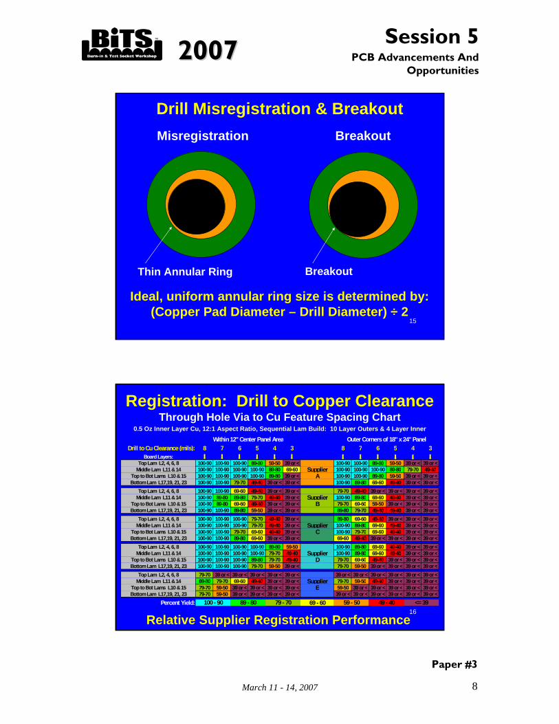
Drill Misregistration & BreakoutBreakout
Breakout
Misregistration
Thin Annular Ring
Ideal, uniform annular ring size is determined by:(Copper Pad Diameter – Drill Diameter) ÷ 2
16
Registration: Drill to Copper ClearanceThrough Hole Via to Cu Feature Spacing Chart
0.5 Oz Inner Layer Cu, 12:1 Aspect Ratio, Sequential Lam Build: 10 Layer Outers & 4 Layer Inner
Drill to Cu Clearance (mils): 8 7 6 5 4 3 8 7 6 5 4 3Board Layers:
Top Lam L2, 4, 6, 8 100-90 100-90 100-90 89-80 59-50 39 or < 100-90 100-90 89-80 59-50 39 or < 39 or <Middle Lam L11 & 14 100-90 100-90 100-90 100-90 89-80 69-60 Supplier 100-90 100-90 100-90 89-80 79-70 49-40
Top to Bot Lams L10 & 15 100-90 100-90 100-90 100-90 89-80 39 or < A 100-90 100-90 89-80 59-50 39 or < 39 or <Bottom Lam L17,19, 21, 23 100-90 100-90 79-70 49-40 39 or < 39 or < 100-90 89-80 69-60 49-40 39 or < 39 or <
Top Lam L2, 4, 6, 8 100-90 100-90 69-60 49-40 39 or < 39 or < 79-70 49-40 39 or < 39 or < 39 or < 39 or <Middle Lam L11 & 14 100-90 89-80 89-80 79-70 49-40 39 or < Supplier 100-90 89-80 69-60 49-40 39 or < 39 or <
Top to Bot Lams L10 & 15 100-90 89-80 69-60 49-40 39 or < 39 or < B 79-70 69-60 59-50 39 or < 39 or < 39 or <Bottom Lam L17,19, 21, 23 100-90 100-90 89-80 59-50 39 or < 39 or < 89-80 79-70 49-40 49-40 39 or < 39 or <
Top Lam L2, 4, 6, 8 100-90 100-90 100-90 79-70 49-40 39 or < 89-80 69-60 49-40 39 or < 39 or < 39 or <Middle Lam L11 & 14 100-90 100-90 100-90 79-70 49-40 39 or < Supplier 100-90 89-80 69-60 49-40 39 or < 39 or <
Top to Bot Lams L10 & 15 100-90 100-90 79-70 69-60 49-40 39 or < C 100-90 79-70 69-60 49-40 39 or < 39 or <Bottom Lam L17,19, 21, 23 100-90 100-90 89-80 69-60 39 or < 39 or < 69-60 49-40 39 or < 39 or < 39 or < 39 or <
Top Lam L2, 4, 6, 8 100-90 100-90 100-90 100-90 89-80 59-50 100-90 89-80 69-60 49-40 39 or < 39 or <Middle Lam L11 & 14 100-90 100-90 100-90 100-90 79-70 49-40 Supplier 100-90 89-80 69-60 49-40 39 or < 39 or <
Top to Bot Lams L10 & 15 100-90 100-90 100-90 89-80 79-70 49-40 D 79-70 69-60 49-40 39 or < 39 or < 39 or <Bottom Lam L17,19, 21, 23 100-90 100-90 100-90 79-70 59-50 39 or < 79-70 59-50 39 or < 39 or < 39 or < 39 or <
Top Lam L2, 4, 6, 8 79-70 39 or < 39 or < 39 or < 39 or < 39 or < 39 or < 39 or < 39 or < 39 or < 39 or < 39 or <Middle Lam L11 & 14 89-80 79-70 69-60 49-40 39 or < 39 or < Supplier 79-70 59-50 49-40 39 or < 39 or < 39 or <
Top to Bot Lams L10 & 15 79-70 59-50 39 or < 39 or < 39 or < 39 or < E 59-50 39 or < 39 or < 39 or < 39 or < 39 or <Bottom Lam L17,19, 21, 23 79-70 59-50 39 or < 39 or < 39 or < 39 or < 39 or < 39 or < 39 or < 39 or < 39 or < 39 or <
Percent Yield: 69 - 60 <= 39100 - 90 89 - 80 79 - 70
Within 12" Center Panel Area Outer Corners of 18" x 24" Panel
59 - 50 49 - 40
Relative Supplier Registration Performance

20072007Session 5
March 11 - 14, 2007
Paper #3
9
PCB Advancements And Opportunities
17
Quality: Resistance Measurements
Supplier C: Significantly High
Through Hole Via Resistance
0
0.5
1
1.5
2
2.5
3
3.5
4
4.5
10 / 18:1 12 / 15:1 13.5 / 13:1 14.5 / 12:1
Drill Diameter (mils) / Aspect Ratio
Ave
rage
Res
ista
nce
(Ohm
s)
Supplier ASupplier BSupplier CSupplier DSupplier E
A B C D E A B C D E A B C D E A B C D E
18
Quality: Resistance Variation
Supplier D: Consistently Lowest
Through Hole Via Resistance Variation
0
10
20
30
40
50
60
70
80
90
100
10 / 18:1 12 / 15:1 13.5 / 13:1 14.5 / 12:1
Drill Diameter (mils) / Aspect Ratio
Coe
ffici
ent o
f Var
iatio
n (%
)
Supplier ASupplier BSupplier CSupplier DSupplier E
A B C D E A B C D E A B C D E A B C D E
20072007Session 5
March 11 - 14, 2007
Paper #3
10
PCB Advancements And Opportunities
19
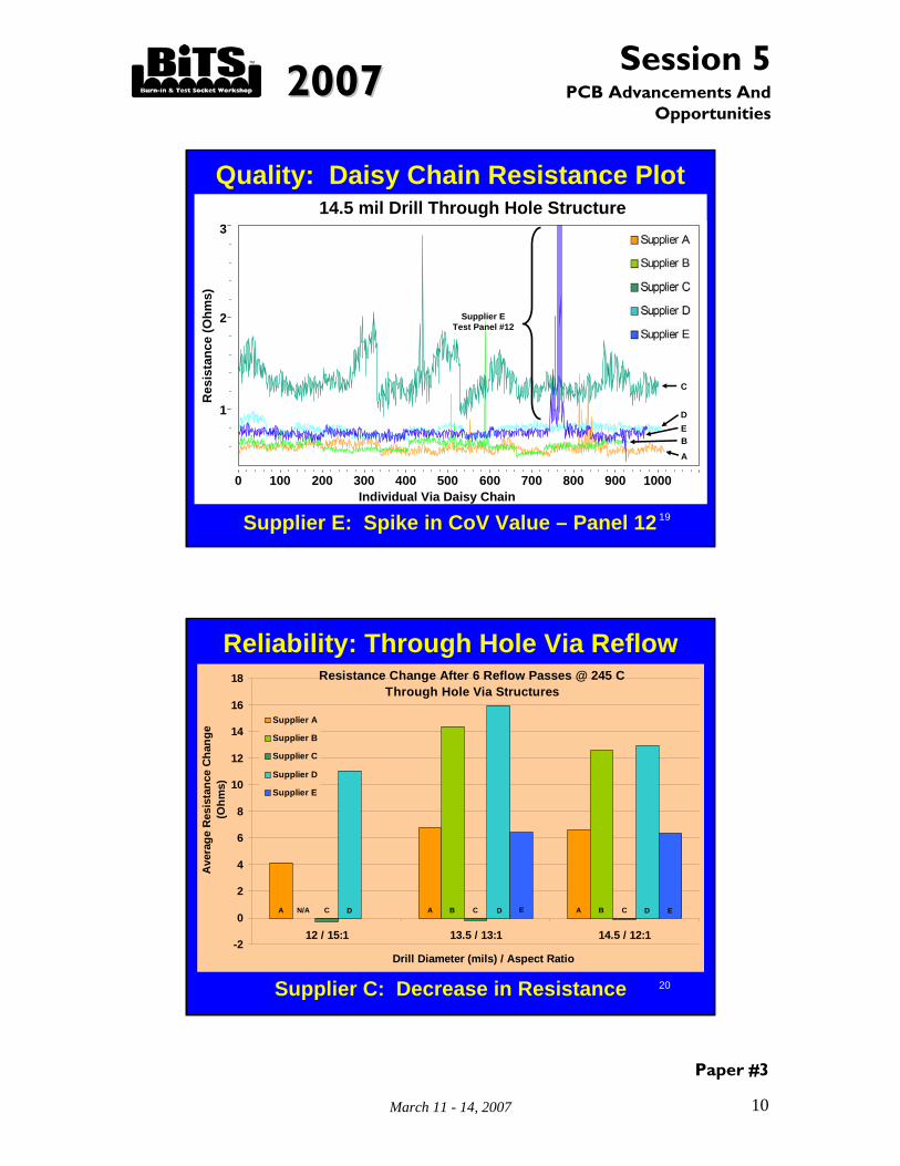
1
2
3
Res
ista
nce
(Ohm
s)
0 100 200 300 400 500 600 700 800 900 1000Individual Via Daisy Chain
14.5 mil Drill Through Hole Structure
C
DE
A
B
Supplier ETest Panel #12
Quality: Daisy Chain Resistance Plot
Supplier E: Spike in CoV Value – Panel 12
20
Reliability: Through Hole Via Reflow
Supplier C: Decrease in Resistance
Resistance Change After 6 Reflow Passes @ 245 CThrough Hole Via Structures
-2
0
2
4
6
8
10
12
14
16
18
12 / 15:1 13.5 / 13:1 14.5 / 12:1
Drill Diameter (mils) / Aspect Ratio
Ave
rage
Res
ista
nce
Cha
nge
(Ohm
s)
Supplier A
Supplier B
Supplier C
Supplier D
Supplier E
A A AC C CD D D EN/A B BE

20072007Session 5
March 11 - 14, 2007
Paper #3
11
PCB Advancements And Opportunities
21
Reliability: Through Hole Via HATS
Supplier C: Survived 500 Thermal Cycles
Highly Accelerated Thermal Shock (HATS), -40 to 145 CThrough Hole Via Structures
0
50
100
150
200
250
300
350
400
450
500
12 / 15:1 13.5 / 13:1 14.5 / 12:1 12 / 15:1 13.5 / 13:1 14.5 / 12:1
10% Change in Resistance Open Circuit
Ave
rage
Num
ber o
f HA
TS C
ycle
s Supplier A
Supplier B
Supplier C
Supplier D
Supplier E
A A A A A A CCCCCC E E E E
Drill Diameter (mils) / Aspect Ratio
22
Reliability: Laser Drilled Microvias
H ig h ly A c c e le r a te d T h e r m a l S h o c k (H A T S ) , -4 0 to 1 4 5 CL a s e r D r i l l e d M ic r o v ia S t r u c tu r e s , A l l A p p l ic a b le S u p p l ie r s
0
1 0 0
2 0 0
3 0 0
4 0 0
5 0 0
3 4 5 6 7 8 9 1 0 3 4 5 6 7 8 9 1 0
1 0 % C h a n g e in R e s is ta n c e O p e n C irc u i t
D r i l l D ia m e te r (m i ls )
Ave
rage
Num
ber o
f
HA
TS C
ycle
s
R e s i s ta n c e C h a n g e A f te r 6 R e f l o w P a s s e s , 2 4 5 CL a s e r D r i l l M i c r o v i a S t r u c tu r e s , A l l A p p l ic a b l e S u p p l i e r s
- 0 . 0 0 5
0 . 0 0 5
0 . 0 1 5
0 . 0 2 5
3 4 5 6 7 8 9 1 0D r i l l D ia m e t e r ( m i l s )
Ave
rage
Res
ista
nce
Cha
nge
(Ohm
s)
0
6.2 Ohms
Few Cycles Between 10% Change and Open

20072007Session 5
March 11 - 14, 2007
Paper #3
12
PCB Advancements And Opportunities
23
Reliability: Blind & Buried Via Reflow Resistance Change After 6 Reflow Passes, @ 245 C
Blind & Buried Via Structures
3.77
1
4.65
5
2.68
3
0.00
0
0.01
3
0.01
3
0.01
3
0.00
0
2.78
9
1.02
0
0.32
4
3.23
2
0.03
1
0.02
2
0.02
1
1.12
7
0
0.02
0.04
0.06
8 / 6:1 10 / 5:1 12 / 4.5:1 13.5 / 4:1 6 / 3:1 8 / 2.5:1 10 / 2:1 12 / 1.5:1
10 Layer Blind Via 4 Layer Buried Via
Drill Diameter (mils) / Aspect Ratio
Ave
rage
Res
ista
nce
Cha
nge
(Ohm
s)
Supplier A
Supplier B
Supplier C
Supplier D
A B C N/A A B C D A B C D A B C D A N/A C D A B C D A B C D A B C D
Supplier A: Consistent Smallest Change
24
Reliability: Blind Via HATS
Supplier B: Earliest Thermal Shock Failure
Highly Accelerated Thermal Shock (HATS), -40 to 145 C10 Layer Blind Via Structures
050
100150200250300350400450500
8 / 6:1 10 / 5:1 12 / 4.5:1 13.5 / 4:1 8 / 6:1 10 / 5:1 12 / 4.5:1 13.5 / 4:1
10% Change in Resistance Open Circuit
Drill Diameter (mils) / Aspect Ratio
Ave
rage
Num
ber o
f HA
TS C
ycle
s
Supplier A
Supplier B
Supplier C
Supplier D
A B C N/A A B C D A B C D A B C D A B C DA B C N/A A B C D A B C D

20072007Session 5
March 11 - 14, 2007
Paper #3
13
PCB Advancements And Opportunities
25
Reliability: Buried Via HATS
Supplier A: Max 500 Shock Cycles on All
Highly Accelerated Thermal Shock (HATS), -40 to 145 C4 Layer Buried Via Structures
050
100150200250300350400450500
6 / 3:1 8 / 2.5:1 10 / 2:1 12 / 1.5:1 6 / 3:1 8 / 2.5:1 10 / 2:1 12 / 1.5:1
10% Change in Resistance Open Circuit
Drill Diameter (mils) / Aspect Ratio
Ave
rage
Num
ber o
f HA
TS C
ycle
s Supplier A
Supplier B
Supplier C
Supplier D
A N/A C D A B C D A B C D A B C D A N/A C D A B C D A B C D A B C D
26
Supplier Relative ResultsThrough Hole Structure Dashboard
No supplier excelled in all test aspects
Defect Density Registration Resistance Values
Resistance Variation Reflow Reliability Thermal Shock
SUPP A BEST BEST OK MIDDLE MIDDLE MIDDLE
SUPP B MIDDLE MIDDLE OK MIDDLE WORST WORST
SUPP C MIDDLE MIDDLE HIGH WORST BEST BEST
SUPP D BEST BEST OK BEST WORST WORST
SUPP E WORST WORST OK MIDDLE WORST WORST

20072007Session 5
March 11 - 14, 2007
Paper #3
14
PCB Advancements And Opportunities
27
ObservationsAspect Ratios
• High defect densities at 18:1, some supp. at 15:1
Laser vs. Mech. Microvias• Mechanically drilled microvias yielded poorly
Back Drill• Larger defect rate than anticipated
Thermal Stress• Supplier through hole reliability did not correlate to pre-reflow resistance & variation measurements
28
Actions Taken & PlansSuppliers:
• Analysis report assessments
• Corrective actions
• New equipment purchases
• Process alignments

20072007Session 5
March 11 - 14, 2007
Paper #3
15
PCB Advancements And Opportunities
29
Actions Taken & PlansSupplier Equipment Implementations
• On-site Laser Drill
• In-line Develop / Etch / Strip
• Reverse Pulse Plating
• Laser Direct Imaging
• Additional Drills & Presses
• Vision Drilling
• Post-Etch Punch
30
Actions Taken & PlansInternal:
• Design Rules & Protocol
• 2nd Test Submissions in 2007
• Overseas Supplier Evaluations
• Burn-in Board Supplier Study
In Conclusion:The PCQR2 Database Provides an
Effective, Quantified, & Impartial Base toCompare PCB Fabrication Suppliers

20072007Session 5
March 11 - 14, 2007
Paper #3
16
PCB Advancements And Opportunities
31
AcknowledgementsMike KorsonTI Make PCB DevelopmentDavid ReedTI Make InfrastructureDavid WolfConductor Analysis TechnologiesTimothy EstesConductor Analysis TechnologiesIPC PCQR2 Database Participating TI PCB Supplier Partners
32
Additional Information & Contacts
PCQR2: www.pcbquality.comCAT Inc: www.cat-test.infoIPC: www.ipc.orgHATS: www.hats-tester.com
David Wolf, Conductor Analysis Technologies [email protected]
Bill Mack, Texas Instruments [email protected]