system level benchmarking analysis - leistungsstark · system level benchmarking analysis of the...
TRANSCRIPT
System Level Benchmarking Analysis
of the Cortex™-A9 MPCore™
This project in ARM is in part
funded by ICT-eMuCo, a
European project supported
under the Seventh Framework
Programme (7FP) for research
and technological development
Roberto Mijat
Software Solutions Architect - ARM
2
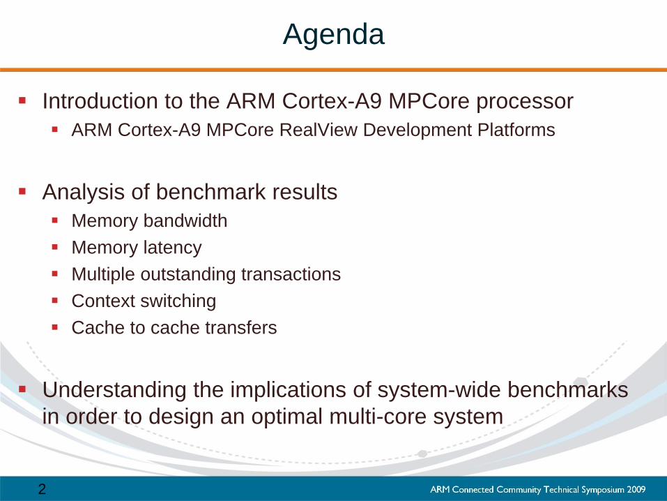
Agenda
Introduction to the ARM Cortex-A9 MPCore processor
ARM Cortex-A9 MPCore RealView Development Platforms
Analysis of benchmark results
Memory bandwidth
Memory latency
Multiple outstanding transactions
Context switching
Cache to cache transfers
Understanding the implications of system-wide benchmarks
in order to design an optimal multi-core system

3
Acknowledgements
ICT-eMuCo
Embedded multi-core processing for mobile communication systems
Research program sponsored by the EU
Partaken by industrial partners (incl. ARM) and top university
From ARM
Anirban Lahiri – Technology Researcher
John Goodacre – Director of Program Management, Processor Division
Adya Shrotriya – Intern
Nicolas Zea – Intern
This project in ARM is in part
funded by ICT-eMuCo, a
European project supported
under the Seventh Framework
Programme (7FP) for research
and technological development
4
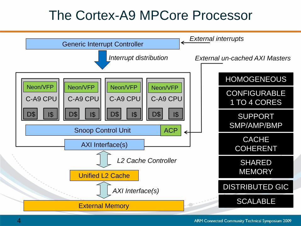
The Cortex-A9 MPCore Processor
External Memory
Snoop Control Unit
D$ I$
C-A9 CPU
D$ I$
C-A9 CPU
D$ I$
C-A9 CPU
D$ I$
C-A9 CPU
Generic Interrupt Controller
Unified L2 Cache
Neon/VFP Neon/VFP Neon/VFP Neon/VFP
External interrupts
Interrupt distribution
AXI Interface(s)
L2 Cache Controller
AXI Interface(s)
ACP
External un-cached AXI Masters
HOMOGENEOUS
SUPPORT
SMP/AMP/BMP
SHARED
MEMORY
CACHE
COHERENT
CONFIGURABLE
1 TO 4 CORES
DISTRIBUTED GIC
SCALABLE
5
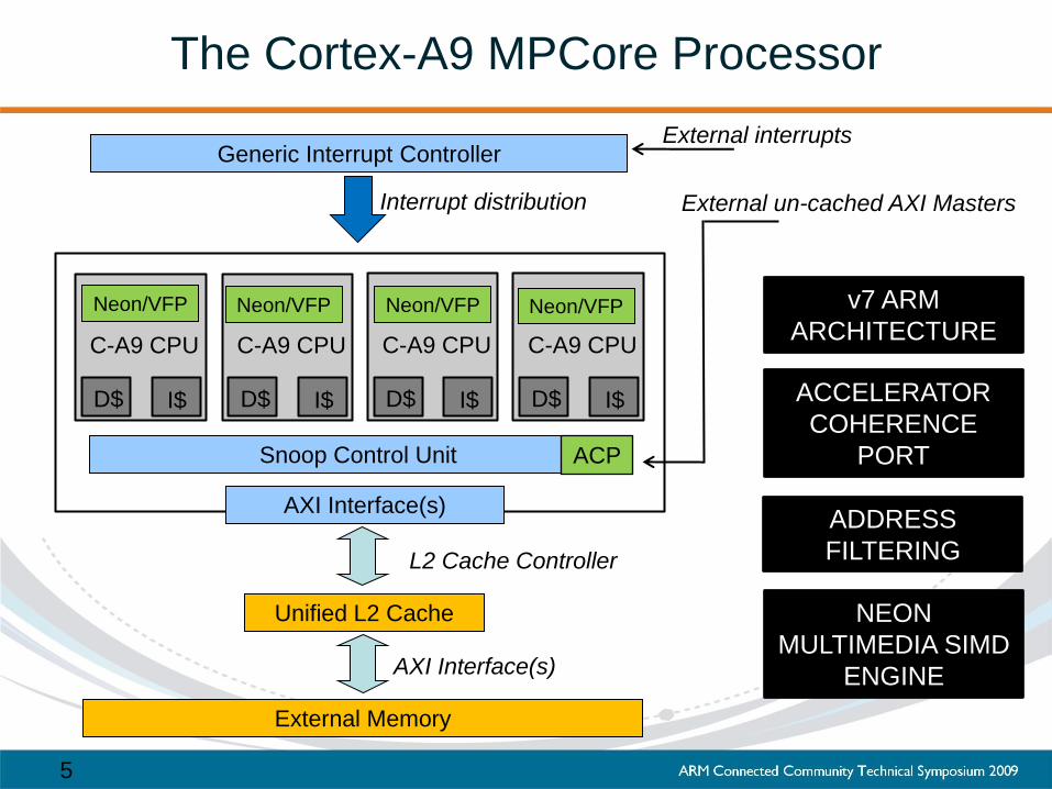
The Cortex-A9 MPCore Processor
External Memory
Snoop Control Unit
D$ I$
C-A9 CPU
D$ I$
C-A9 CPU
D$ I$
C-A9 CPU
D$ I$
C-A9 CPU
Generic Interrupt Controller
Unified L2 Cache
Neon/VFP Neon/VFP Neon/VFP Neon/VFP
External interrupts
Interrupt distribution
AXI Interface(s)
L2 Cache Controller
AXI Interface(s)
ACP
External un-cached AXI Masters
ACCELERATOR
COHERENCE
PORT
ADDRESS
FILTERING
NEON
MULTIMEDIA SIMD
ENGINE
v7 ARM
ARCHITECTURE

6
Superscalar out-of-order
instruction execution
Up to 4 instruction cache line
pre-fetching
Decode up to TWO full
instructions per cycle and
dispatch up to FOUR
Register renaming for
speculative execution and
loop unrolling
FPU/NEON
Counters for performance
monitoring and PTM
Cortex-A9: Technology Leadership
Recently announced
hard macro 40nm G (TSMC) implementation targeting 2GHz
7
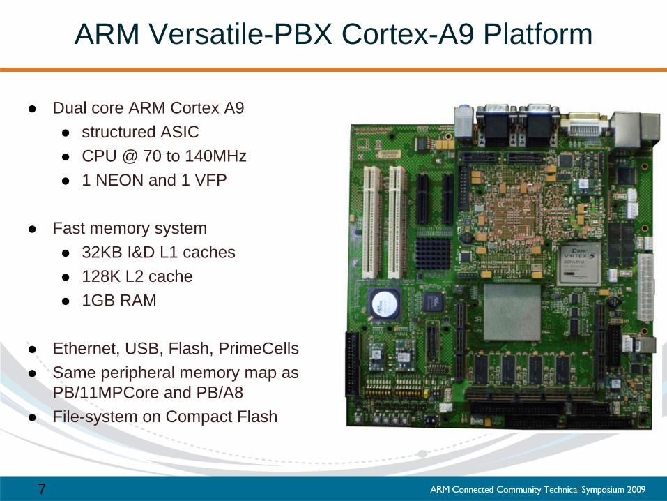
ARM Versatile-PBX Cortex-A9 Platform
Dual core ARM Cortex A9
structured ASIC
CPU @ 70 to 140MHz
1 NEON and 1 VFP
Fast memory system
32KB I&D L1 caches
128K L2 cache
1GB RAM
Ethernet, USB, Flash, PrimeCells
Same peripheral memory map as
PB/11MPCore and PB/A8
File-system on Compact Flash
8
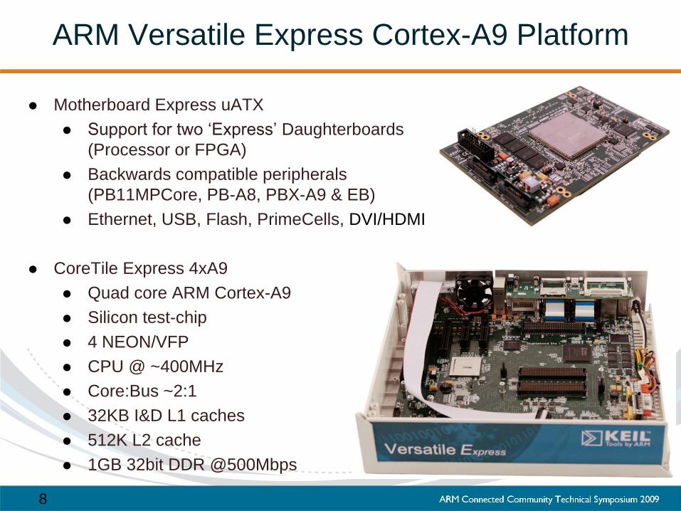
ARM Versatile Express Cortex-A9 Platform
Motherboard Express uATX
Support for two „Express‟ Daughterboards
(Processor or FPGA)
Backwards compatible peripherals
(PB11MPCore, PB-A8, PBX-A9 & EB)
Ethernet, USB, Flash, PrimeCells, DVI/HDMI
CoreTile Express 4xA9
Quad core ARM Cortex-A9
Silicon test-chip
4 NEON/VFP
CPU @ ~400MHz
Core:Bus ~2:1
32KB I&D L1 caches
512K L2 cache
1GB 32bit DDR @500Mbps

11
Software Framework for Benchmarks
Linux kernel 2.6.28
from kernel.org
pre-built images, boot-loaders, patches, file-systems etc
available from ARM website
Debian 5.0 “Lenny” Linux file-system
compiled for v4T
12
lmbench3 benchmark
Comprehensive system benchmark including:
Micro-benchmarks, focusing on:
Bandwidth
Latency
Other (system info diagnostics etc)
Context switching
Stream benchmark
Version 3 provides infrastructure to measure the scalability of
multi-processor systems
Concurrent execution and accurate timing infrastructure
Break out of the boundaries of L1 cache subsystem
For the purpose of this presentation we‟ll only look at a small
subset of these benchmarks

13
Memory Bandwidth – PBX-A9
Single Instance 2 Instances
Consider a 2 core platform
Knees indicate cache sizes (small [128k] L2 RAM for PBX-A9)
Increased effective memory bandwidth for multicore (2 cores)
Cache bandwidth – doubles
DDR2 memory bandwidth – doubles
Agnostic to alignment
Note: Pre-fetching disabled for normalization
14
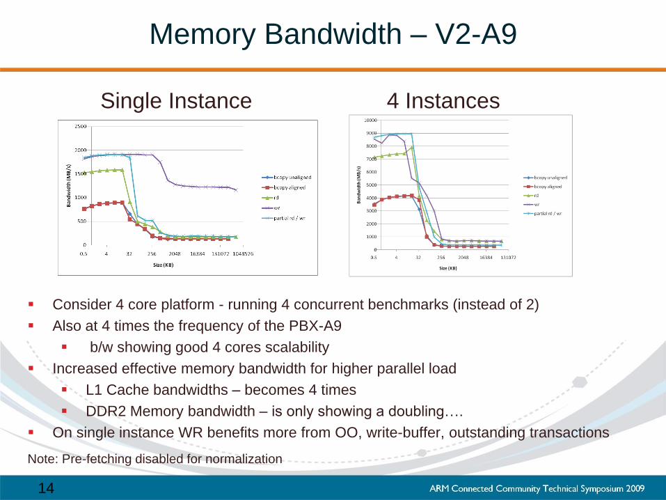
Memory Bandwidth – V2-A9
Single Instance 4 Instances
Consider 4 core platform - running 4 concurrent benchmarks (instead of 2)
Also at 4 times the frequency of the PBX-A9
b/w showing good 4 cores scalability
Increased effective memory bandwidth for higher parallel load
L1 Cache bandwidths – becomes 4 times
DDR2 Memory bandwidth – is only showing a doubling….
On single instance WR benefits more from OO, write-buffer, outstanding transactions
Note: Pre-fetching disabled for normalization
15
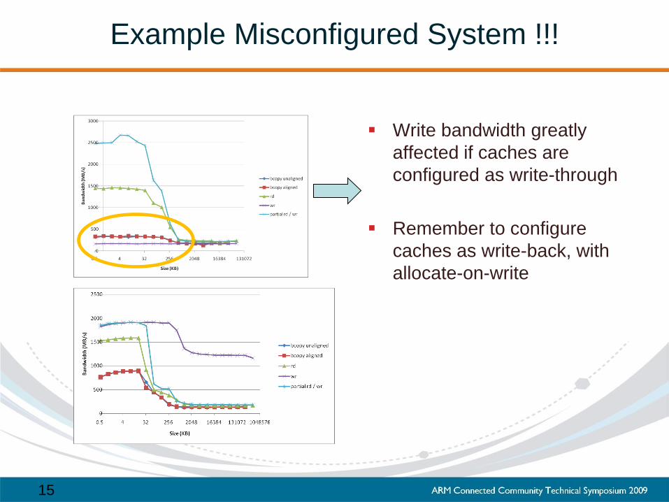
Example Misconfigured System !!!
Write bandwidth greatly
affected if caches are
configured as write-through
Remember to configure
caches as write-back, with
allocate-on-write

16
Bandwidth-Latency Relation
Latency determines
the response time
for applications on
a multicore
Applications
requiring short
bursts of memory
accesses can run
concurrently with
bandwidth heavy
applications without
any observable
degradation – if
latency remains
constant
Core0 Core1Internet Browser
Video / Image
Processing
17
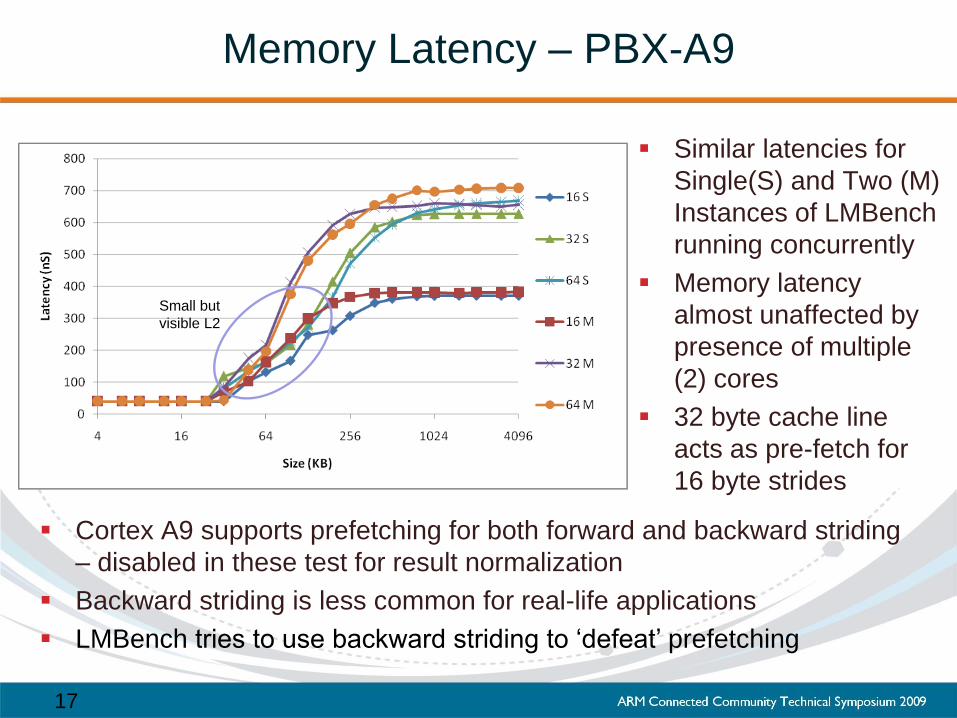
Memory Latency – PBX-A9
Similar latencies for
Single(S) and Two (M)
Instances of LMBench
running concurrently
Memory latency
almost unaffected by
presence of multiple
(2) cores
32 byte cache line
acts as pre-fetch for
16 byte strides
Cortex A9 supports prefetching for both forward and backward striding
– disabled in these test for result normalization
Backward striding is less common for real-life applications
LMBench tries to use backward striding to „defeat‟ prefetching
Small but
visible L2

18
Memory Latency – V2
4 Instances of LMBench running - 4 times the application load
Memory latency goes up only by about 20%
32 byte cache line acts as pre-fetch for 16 byte strides
Application on one CPU mostly unaffected by execution on other CPUs
Within the limits of memory bandwidth to DDR Memory
Single Instance 4 Instances
19
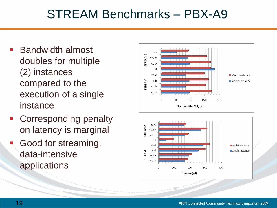
STREAM Benchmarks – PBX-A9
Bandwidth almost
doubles for multiple
(2) instances
compared to the
execution of a single
instance
Corresponding penalty
on latency is marginal
Good for streaming,
data-intensive
applications

20
L2 Latency Configuration
PL310 allows configuring
the latencies for the L2
cache data & tag RAMs
Optimization: Find the
minimal latency value for
which the system would
still work
The difference in
performance can be
double or more
Remember DDR
memory controllers
(PL34x) have similar
setting
Additional
Latency
(cycles)

21
Memory Load Parallelism
Indicates the number of possible
outstanding reads
Memory system design
determines the ability of the
processor to hide memory
latency
Support for number of
outstanding read/writes essential
for multicores – fully supported
by PL310 / PL34x
L1 supports 4 linefill requests on
average while the implemented
DDR2 memory system 2
Systems should support as much
memory parallelization as
possible
22
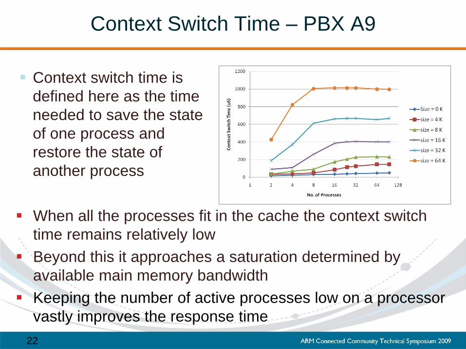
Context Switch Time – PBX A9
When all the processes fit in the cache the context switch
time remains relatively low
Beyond this it approaches a saturation determined by
available main memory bandwidth
Keeping the number of active processes low on a processor
vastly improves the response time
Context switch time is
defined here as the time
needed to save the state
of one process and
restore the state of
another process

23
Context Switching Time – PBX A9
Peak context switch time increases by a small fraction ( < 20%)
Indicates that context switches on separate processors are almost mutually
orthogonal and enables the MPCore to support more active tasks than a
single core time-sliced processor before the system becomes unresponsive
Single Instance 2 Instances

24
A memory system optimized for MP
MODIFIED - Coherent
cache line is not up to
date with main memory
EXCLUSIVE - Up to date
and no other copies exist
SHARED - Coherent cache
line which is up to date
with main memory
INVALID - This coherent
cache line is not present
in the cache
In a MESI compliant SMP system,
every cache line is marked with
one of the four following states:
DUPLICATED TAG RAMs
DIRECT DATA INTERVENTION
MIGRATORY LINES
Stored in Snoop Control Unit for quicker access
Process of checking if requested data is in other
CPUs‟ caches is performed without accessing them
(cache-2-cache transfer)
Copy clean data from one CPU cache to another
Move dirty data from one CPU to another
and skip MESI shared state
Avoids writing to L2/L3 and reading the data
back from external memory
ARM MPCore processors implement
optimizations to the MESI protocol:

Modified → Shared
CPU 1
Memory
CPU 2
Writeback Linefill
Read from cache line
M → S I → S
Request

Exclusive → Shared
CPU 1
Memory
CPU 2
Linefill
Read from cache line
E → S I → S
Request

27
Cache to Cache Latency
Significant benefits
achievable if the
working set of the
application partitioned
between the cores can
be contained within the
sum of their caches
Helpful for streaming
data between cores
may be used in
conjunction with
interrupts between
cores
Though dirty lines have higher
latency they still have 50%
performance benefit
28
Summary and Recommendations
Memory bandwidth may be increased by
Increasing size of cache lines
Increasing width of memory bus/interface
Interleave accesses (and buffer reads/writes)
Memory latency can be improved by
Shortening paths
Increasing rate of successful pre-fetching
Understanding the current latencies in a system
Spreading Memory and CPU intensive applications over the
multiple cores provides better performance
Subject to bandwidth and latencies of memory system
ARM MPCore architecture mitigates migration overheads
Running multiple memory intensive applications on a single CPU can
be detrimental due to cache conflicts