title goes here subhead goes here - ebeam · •full chip mb-mdp 2013 ... •incorporating ebeam...
TRANSCRIPT

5th Annual eBeam Initiative Luncheon SPIE – February 26, 2013
Aki Fujimura
CEO – D2S, Inc.
Managing Company Sponsor – eBeam Initiative

eBeam Writes All Chips
3
The eBeam Initiative:
• Is an educational
platform for eBeam
technology and its
impact on all
lithography approaches
• Open to any company
in the semiconductor
design chain with an
interest in eBeam
technologies
DSA
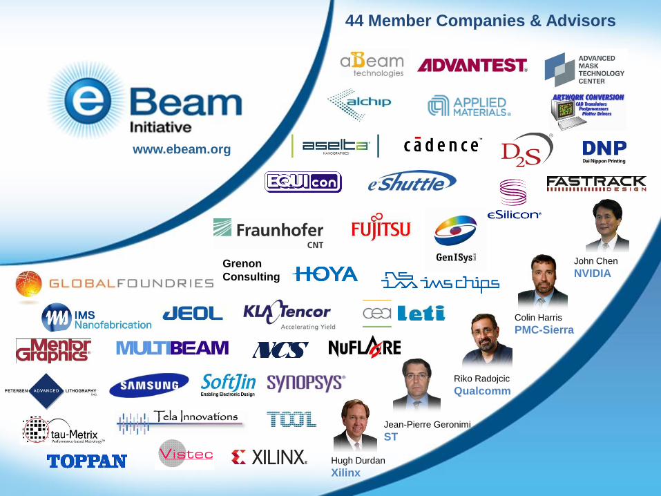
44 Member Companies & Advisors
www.ebeam.org
Colin Harris
PMC-Sierra
Riko Radojcic
Qualcomm
Jean-Pierre Geronimi
ST
Grenon
Consulting
John Chen
NVIDIA
Hugh Durdan
Xilinx

Two Industry Veterans
Join as eBeam Initiative Advisors
5
John Chen
NVIDIA
Hugh Durdan
Xilinx

New: The Fine Line Video Journal
Use your new earphones!
6
Shot Talk:
D2S
Tech Talk:
Samsung & D2S
From the White Board:
Ryan Pearman
Perspectives:
Hugh Durdan, Xilinx
Winter 2013 Edition

Design for eBeam (DFeB) Roadmap
Roadmap Themes
• Mask write times
• Total cycle times
• Mask accuracy
• Wafer quality
• Design for eBeam Methodology
2010
•Complex masks
•Overlapping shots – circles, VSB
•Model-based mask data prep (MB-MDP)
2011
•Thermal analysis of overlapping shots
•Dose control for accuracy
•Double simulation for more accurate analysis of wafer quality
2012
• Mask CD Uniformity improvements
• Accurate measure of mask goodness
• Full chip MB-MDP
2013
•Design for eBeam (DFeB) mask methodology
• Incorporating eBeam Initiative technology roadmap
7

8
Wafer Process Enhanced by eBeam
Source: Samsung and D2S at BACUS 2012
• More Complex Shapes on mask
enhance Wafer Process Latitude
• Complex Masks, Manhattanized or
ideal curvilinear, had two problems:
• Poor mask CDU leading to
unreliable results on wafer
• Mask write time
• Samsung and GLOBALFOUNDRIES
studies show MB-MDP solves this
problem

Multibeam Technology Progress eMET POC exposure with 256k-APS ILT device test pattern
ILT device test pattern
Design: DNP
Scanning Stripe
exposure
20nm
beam size
5nm
pixel size
with
PEC
exposure of DNP design
60nm dots
Design
30nm dots
exposure 2-times smaller
Source: IMS Nanofabrication at BACUS 2012
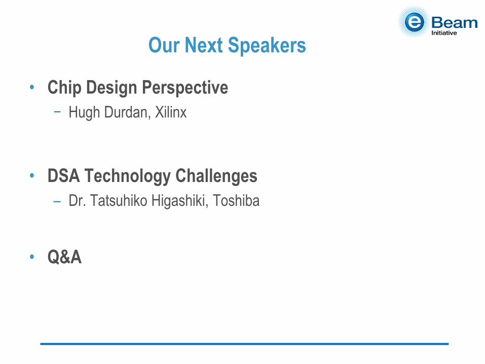
• Chip Design Perspective
− Hugh Durdan, Xilinx
• DSA Technology Challenges
– Dr. Tatsuhiko Higashiki, Toshiba
• Q&A
Our Next Speakers

Hugh Durdan Vice President, Portfolio & Solutions Marketing
Lithography Challenges in Advanced Nodes
– A Design Perspective
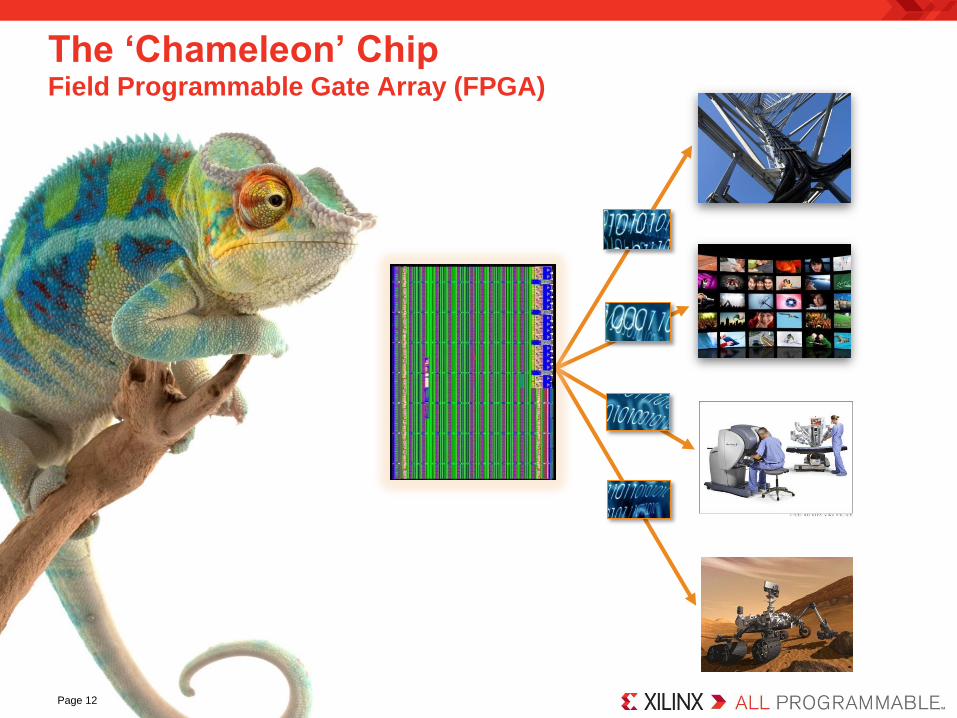
The ‘Chameleon’ Chip Field Programmable Gate Array (FPGA)
Page 12
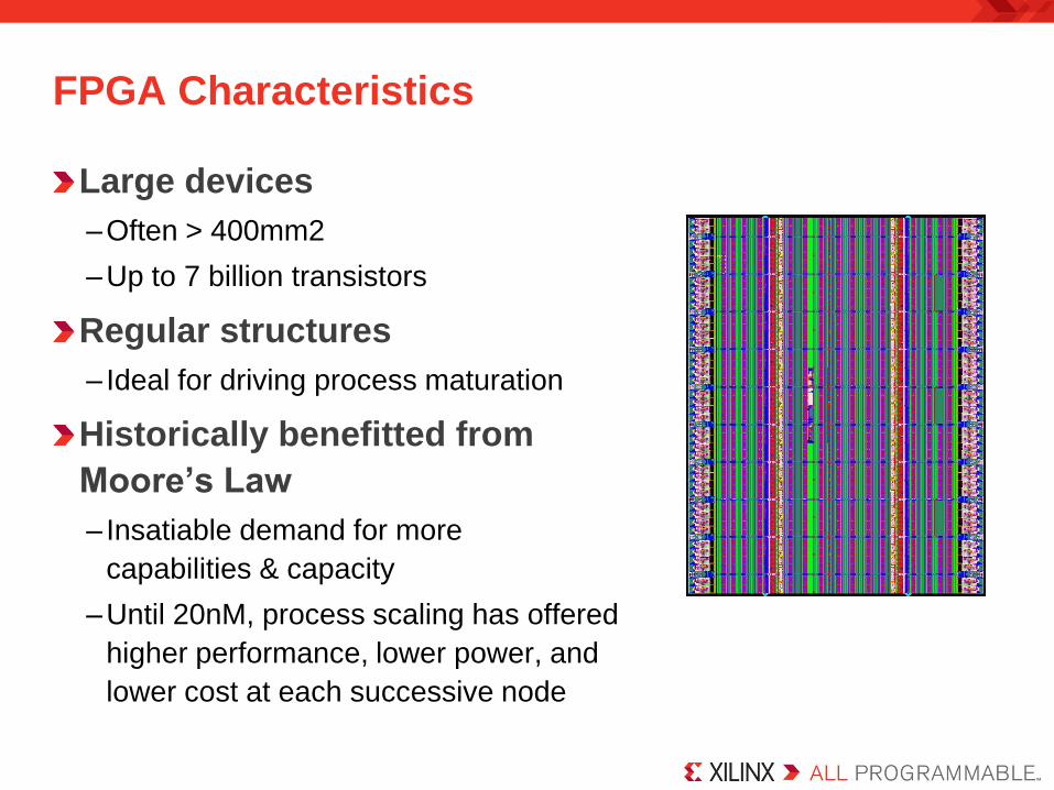
Large devices
–Often > 400mm2
–Up to 7 billion transistors
Regular structures
– Ideal for driving process maturation
Historically benefitted from
Moore’s Law
– Insatiable demand for more
capabilities & capacity
–Until 20nM, process scaling has offered
higher performance, lower power, and
lower cost at each successive node
FPGA Characteristics

More complex transistor
structure = more masks
Double patterning required
for finer features in 20nM
= more masks
Net result is 30% increase in
masking layers
Directly translates into
increased mask and
wafer costs
So What’s Changed?

Mask write time
increases exponentially
– Reduced throughput
– Higher cost per mask
More restrictive
design rules
– Larger die
Reduced CD uniformity
– More design margin
– Lower yields
And Even Worse…
Max. Mask Write Time (Hours)
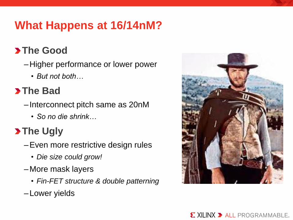
The Good
–Higher performance or lower power
• But not both…
The Bad
– Interconnect pitch same as 20nM
• So no die shrink…
The Ugly
–Even more restrictive design rules
• Die size could grow!
–More mask layers
• Fin-FET structure & double patterning
–Lower yields
What Happens at 16/14nM?
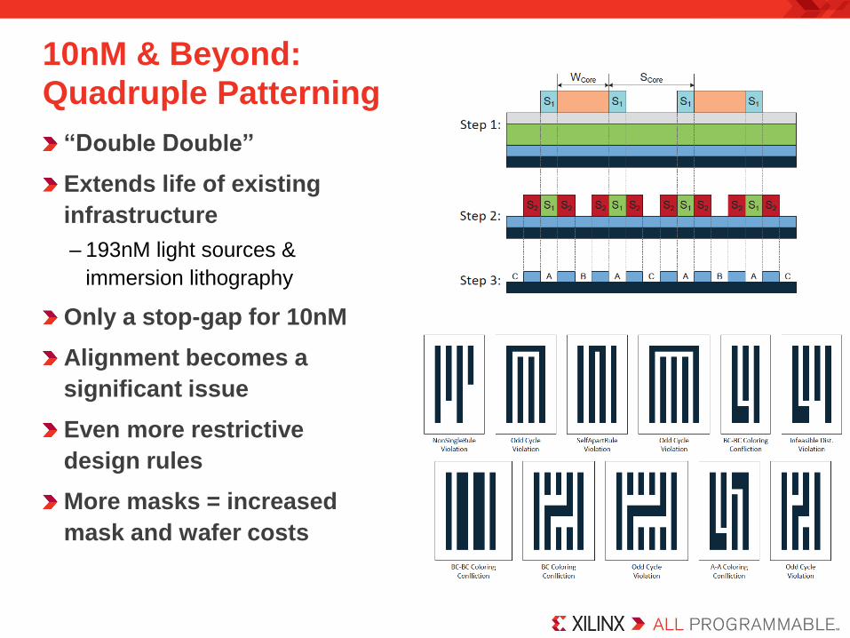
“Double Double”
Extends life of existing
infrastructure
– 193nM light sources &
immersion lithography
Only a stop-gap for 10nM
Alignment becomes a
significant issue
Even more restrictive
design rules
More masks = increased
mask and wafer costs
10nM & Beyond:
Quadruple Patterning
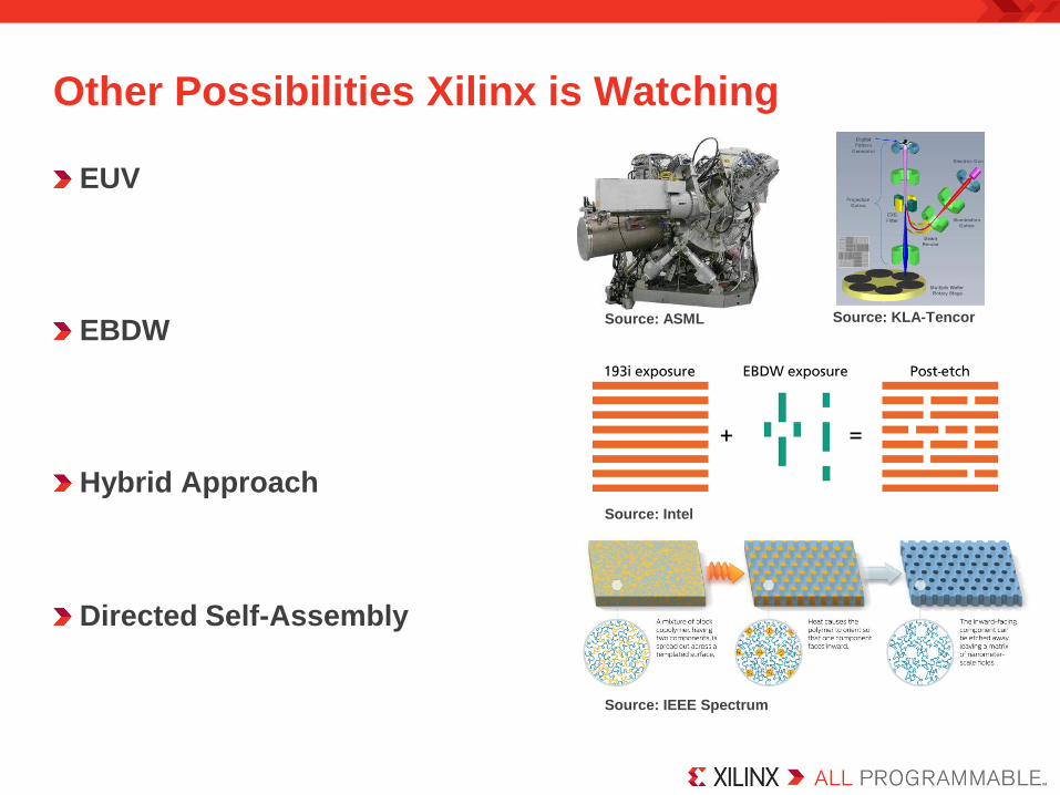
EUV
EBDW
Hybrid Approach
Directed Self-Assembly
Other Possibilities Xilinx is Watching
Source: ASML Source: KLA-Tencor
Source: IEEE Spectrum
Source: Intel

Lithography challenges are a significant threat to maintaining
Moore’s Law
Cost per transistor is going up for the first time in the history of
the semiconductor industry
No good solution on the horizon
– Quadruple patterning only good in the short-term
– EUV immature, expensive, and late
– Direct-write too slow today for volume production
eBeam will be part of the solution
– Better accuracy in mask making to reduce CD variation
– Hybrid approach
– Direct write if throughput can be improved
Perspectives

DSA Technology Challenges
Center for Semiconductor Research & Development
Advanced Lithography Process Technology Dept.
Tatsuhiko Higashiki
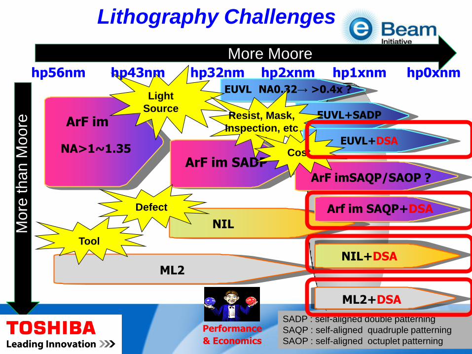
Lithography Challenges
ArF im
NA>1~1.35
EUVL NA0.32→ >0.4x ?
ArF im SADP
Performance
& Economics
EUVL+SADP
Light
Source Resist, Mask,
Inspection, etc
ArF imSAQP/SAOP ?
More Moore
More
than M
oore
ML2
Tool
Defect
NIL
EUVL+DSA
NIL+DSA
hp56nm hp43nm hp32nm hp2xnm hp1xnm hp0xnm
ML2+DSA
Arf im SAQP+DSA
SADP : self-aligned double patterning
SAQP : self-aligned quadruple patterning
SAOP : self-aligned octuplet patterning
Cost
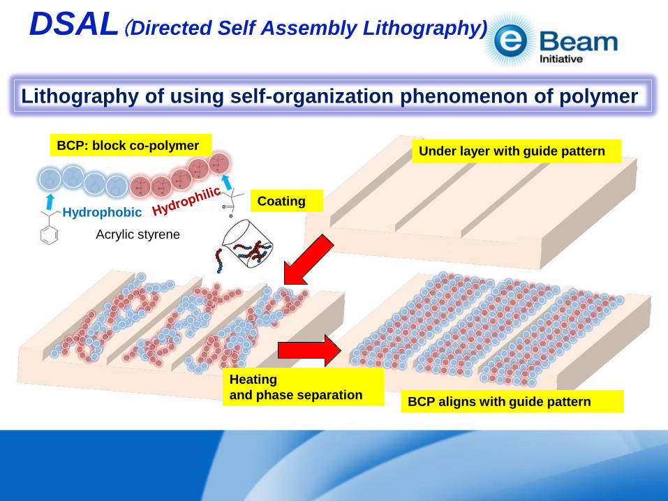
DSAL(Directed Self Assembly Lithography)
Lithography of using self-organization phenomenon of polymer
Acrylic styrene
BCP: block co-polymer
Hydrophobic Coating
Under layer with guide pattern
Heating
and phase separation BCP aligns with guide pattern

Grapho-Epitaxy & Chemo-Epitaxy
Segalmann et al., Adv.Mater. 3,1152(2001) Nato et al., IEEE Trans. Magn.38,1949(2002) Chen et al.,Appl.Phys.Lett.81,3657(2002)
Chen et al.,Adv.Mater. 20,3155(2008) Rulz et al., Science, 321,936(2008) Tada, Macromol.41,9267(2008)
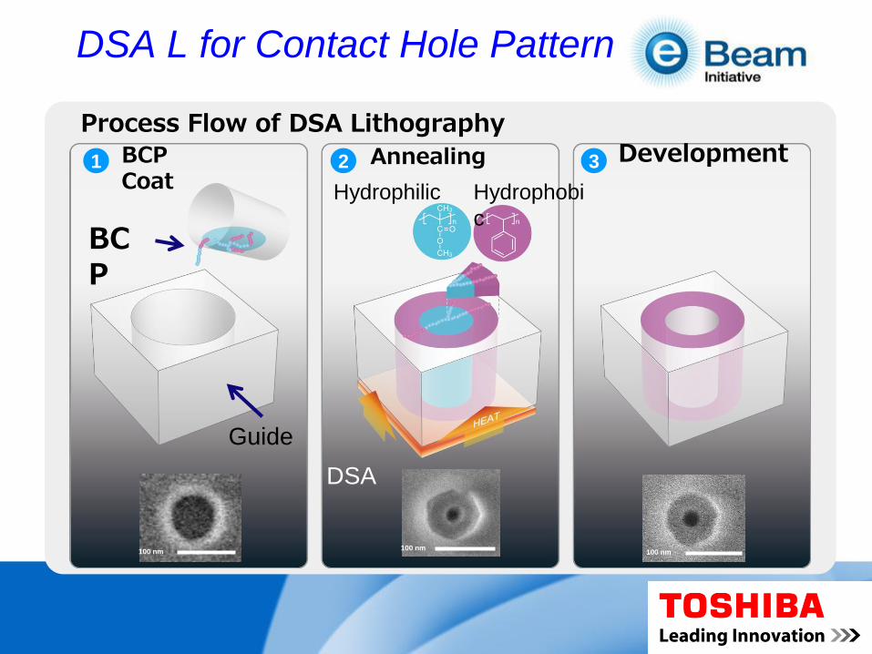
DSA L for Contact Hole Pattern
Process Flow of DSA Lithography
BCP Coat
Annealing Development
100 nm 100 nm
Guide
DSA
Hydrophilic Hydrophobi
c
1 2 3
100 nm
BCP

Layout
Guide Data
OPC Litho Simulation
GDS
DSA Simulation
HotSpot result
OPC
Condition (material/process)
DfM FeedBack
Wafer Process FeedForward APC
Judge
Model
EDA Tool
EDA Tool
DSA OPC/DfM/APC Flow
X-section
Sidewall
Bottom
PS-b-PMMA
Top
Top-down
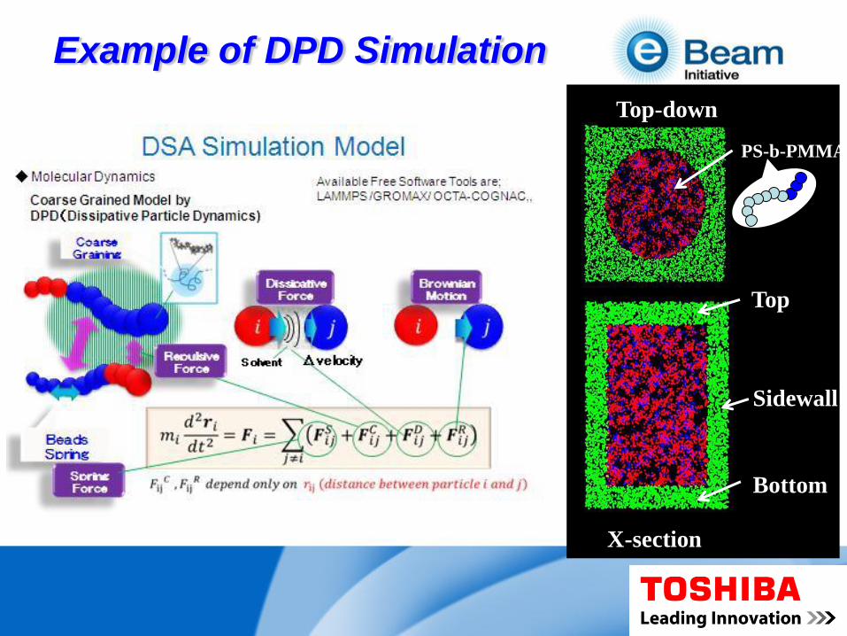
Example of DPD Simulation

Pre
dic
tion
Accura
cy
speed
(<0.25nm)
TAT (1m/10μm2)
Rigorous Model
Shroedinger's Equation etc
Model Self Consistent mean Field Dissipative Particle Dynamics
methodology Based on statistical field theory Based on Newton's motion equation
Challenge Modeling of thermal
fluctuations
Difficult to fit to a measured data
Target
SCF DPD
TAT (5h/10μm2)
(5nm)
DSA Simulation Model
TAT (? years/10μm2)
Impractical model

Conclusion: Challenges for DSAL
• High performance DSA material – Resolution, LWR/LER, Etching
• Long term stability – Robust material and tool for environmental control such as surface energy
stability, temperature, humidity, pressure and PH, etc.
– Defectivity, CD and overlay accuracy
• Metrology & Inspection – Metrology for 3D profile
– Inspection technology for 1xnmhp and beyond needs to overcome t-put vs accuracy/sensitivity trade-off.
• Development of molecular dynamics based DSA simulator – More accurate simulation model
• BCP and related molecular design
• Microphase separation (2D/3D)
• DSA and guide patterning (litho/wet/dry)
– TAT vs accuracy trade-off
• DSA OPC/DFM technology – Design rule verification

2013/2/26

Thank you for attending!
Q & A
30
