tlv2432, tlv2432a, tlv2434, tlv2434a...
TRANSCRIPT

TLV2432, TLV2432A, TLV2434, TLV2434AAdvanced LinCMOS RAIL-TO-RAIL OUTPUT
WIDE-INPUT-VOLTAGE OPERATIONAL AMPLIFIERSSLOS168F – NOVEMBER 1996 – REVISED MARCH 2001
1POST OFFICE BOX 655303 • DALLAS, TEXAS 75265
Output Swing Includes Both Supply Rails
Extended Common-Mode Input VoltageRange . . . 0 V to 4.5 V (Min) with 5-V SingleSupply
No Phase Inversion
Low Noise . . . 18 nV/√Hz Typ at f = 1 kHz
Low Input Offset Voltage 950 µV Max at TA = 25°C (TLV243xA)
Low Input Bias Current . . . 1 pA Typ
Very Low Supply Current . . . 125 µA PerChannel Max
600-Ω Output Drive
Macromodel Included
Available in Q-Temp Automotive HighRel Automotive ApplicationsConfiguration Control / Print SupportQualification to Automotive Standards
description
The TLV243x and TLV243xA are low-voltageoperational amplifier from Texas Instruments. Thecommon-mode input voltage range for eachdevice is extended over the typical CMOSamplifiers making them suitable for a wide rangeof applications. In addition, these devices do notphase invert when the common-mode input isdriven to the supply rails. This satisfies mostdesign requirements without paying a premiumfor rail-to-rail input performance. They also exhibitrail-to-rail output performance for increaseddynamic range in single- or split-supply applica-tions. This family is fully characterized at 3-V and5-V supplies and is optimized for low-voltageoperation. The TLV243x only requires 100 µA(typ) of supply current per channel, making it idealfor battery-powered applications. The TLV243xalso has increased output drive over previousrail-to-rail operational amplifiers and can drive600-Ω loads for telecom applications.
The other members in the TLV243x family are the high-power, TLV244x, and micro-power, TLV2422, versions.
The TLV243x, exhibiting high input impedance and low noise, is excellent for small-signal conditioning forhigh-impedance sources, such as piezoelectric transducers. Because of the micropower dissipation levels andlow-voltage operation, these devices work well in hand-held monitoring and remote-sensing applications. Inaddition, the rail-to-rail output feature with single- or split-supplies makes this family a great choice wheninterfacing with analog-to-digital converters (ADCs). For precision applications, the TLV243xA is available andhas a maximum input offset voltage of 950 µV.
If the design requires single operational amplifiers, see the TI TLV2211/21/31. This is a family of rail-to-rail outputoperational amplifiers in the SOT-23 package. Their small size and low power consumption, make them idealfor high density, battery-powered equipment.
Copyright 2001, Texas Instruments IncorporatedPRODUCTION DATA information is current as of publication date.Products conform to specifications per the terms of Texas Instrumentsstandard warranty. Production processing does not necessarily includetesting of all parameters.
Please be aware that an important notice concerning availability, standard warranty, and use in critical applications ofTexas Instruments semiconductor products and disclaimers thereto appears at the end of this data sheet.
Advanced LinCMOS is a trademark of Texas Instruments.
Figure 1
TA = 125°C
TA = 85°C
TA = 25°C
TA =–40°C
VDD = 5 V
2
1
00 4 8 12
3
4
5
16 20
VO
H –
Hig
h-L
evel
Ou
tpu
t V
olt
age
– V
HIGH-LEVEL OUTPUT VOLTAGEvs
HIGH-LEVEL OUTPUT CURRENT
IOH – High-Level Output Current – A
ÁÁÁÁÁÁ
V OH
On products compliant to MIL-PRF-38535, all parameters are testedunless otherwise noted. On all other products, productionprocessing does not necessarily include testing of all parameters.

TLV2432, TLV2432A, TLV2434, TLV2434AAdvanced LinCMOS RAIL-TO-RAIL OUTPUTWIDE-INPUT-VOLTAGE OPERATIONAL AMPLIFIERSSLOS168F – NOVEMBER 1996 – REVISED MARCH 2001
2 POST OFFICE BOX 655303 • DALLAS, TEXAS 75265
TLV2432 and TLV2432A AVAILABLE OPTIONS
PACKAGED DEVICES
TAVIOmaxAT 25°C
SMALLOUTLINE
(D)
CHIP CARRIER(FK)
CERAMIC DIP(JG)
TSSOP(PW)
CERAMIC FLATPACK
(U)
0°C to 70°C 2.5 mV TLV2432CD — — TLV2432CPW —
40°C to 85°C950 µV TLV2432AID — — TLV2432AIPW —
–40°C to 85°Cµ
2.5 mV TLV2432ID — — — —
40°C to 125°C950 µV TLV2432AQD — — — —
–40°C to 125°Cµ
2.5 mV TLV2432QD — — — —
–55°C to 125°C 950 µV — TLV2432AMFK TLV2432AMJG — TLV2432AMU–55°C to 125°C µ
2.5 mV — TLV2432MFK TLV2432MJG — TLV2432MU
The D packages are available taped and reeled. Add R suffix to device type (e.g., TLV2432CDR). The PW package is available only left-end tapedand reeled.
TLV2434 AVAILABLE OPTIONS
PACKAGED DEVICES
TA VIOmax AT 25°C SMALLOUTLINE
(D)
TSSOP(PW)
0°C to 70°C 2.5 mV TLV2434CD TLV2434CPW
–40°C to 125°C 950 µV TLV2434AID TLV2434AIPW–40°C to 125°C µ
2.5 mV TLV2434ID TLV2434IPW
The D packages are available taped and reeled. Add R suffix to device type (e.g., TLV2434CDR). ThePW package is available only left-end taped and reeled.
1
2
3
4
5
6
7
14
13
12
11
10
9
8
1OUT1IN–1IN+
VDD+2IN+2IN–
2OUT
4OUT4IN–4IN+VDD–/GND3IN+3IN–3OUT
(TOP VIEW)
TLV2434D OR PW PACKAGE
1
2
3
4
8
7
6
5
1OUT1IN–1IN+
VDD – /GND
VDD+2OUT2IN–2IN+
NCVDD +2OUT2IN –2IN +
NC1OUT1IN –1IN +
VDD– /GND
1
2
3
4
5
10
9
8
7
6
TLV2432U PACKAGE(TOP VIEW)
3 2 1 20 19
9 10 11 12 13
4
5
6
7
8
18
17
16
15
14
NC2OUTNC2IN–NC
NC1IN–
NC1IN+
NC
NC
1OU
TN
C2I
N+
NC
NC
NC
NC
VD
D+
VD
D–
TLV2432FK PACKAGE(TOP VIEW)
/GN
D
1
2
3
4
8
7
6
5
1OUT1IN–1IN+
VDD– /GND
VDD+2OUT2IN–2IN+
NC – No internal connection
TLV2432PW PACKAGE
(TOP VIEW)
TLV2432D OR JG PACKAGE
(TOP VIEW)

TLV2432, TLV2432A, TLV2434, TLV2434ARAIL-TO
-RAIL OUTPUT
WIDE-INPUT-VO
LTAGE O
PERATIONAL AM
PLIFIERSS
LOS
168F – N
OV
EM
BE
R 1996 – R
EV
ISE
D M
AR
CH
2001
Advanced LinCMO
S
PO
ST
OF
FIC
E B
OX
655303 DA
LLAS
, TE
XA
S 75265
•3
equivalent schematic (each amplifier)
Q27
R9
Q29Q22
Q23
Q26
Q25
Q24
Q31 Q34 Q36
Q32
Q33 Q35
Q37
D1
Q30
R10
VB3
VB2
VB4
VDD+
VDD–/GND
OUT
R8R1 R2
Q2 Q5
Q1 Q4
Q3
Q12
Q11
Q10Q6
Q7
Q8
Q9
VB3
VB4
C1
C2
C3
R5
R6
Q13 Q15
Q16
Q17
Q14
Q19
Q18
Q20
Q21
R7R3 R4
VB2
IN+
IN–
VB1
COMPONENTCOUNT
TransistorsDiodesResistorsCapacitors
695
266

TLV2432, TLV2432A, TLV2434, TLV2434AAdvanced LinCMOS RAIL-TO-RAIL OUTPUTWIDE-INPUT-VOLTAGE OPERATIONAL AMPLIFIERSSLOS168F – NOVEMBER 1996 – REVISED MARCH 2001
4 POST OFFICE BOX 655303 • DALLAS, TEXAS 75265
absolute maximum ratings over operating free-air temperature range (unless otherwise noted)†
Supply voltage, VDD (see Note 1) 12 V. . . . . . . . . . . . . . . . . . . . . . . . . . . . . . . . . . . . . . . . . . . . . . . . . . . . . . . . . . . . Differential input voltage, VID (see Note 2) ±VDD. . . . . . . . . . . . . . . . . . . . . . . . . . . . . . . . . . . . . . . . . . . . . . . . . . . Input voltage, VI (any input, see Note 1): C and I suffix –0.3 V to VDD. . . . . . . . . . . . . . . . . . . . . . . . . . . . . . . . Input current, II (each input) ±5 mA. . . . . . . . . . . . . . . . . . . . . . . . . . . . . . . . . . . . . . . . . . . . . . . . . . . . . . . . . . . . . . . Output current, IO ±50 mA. . . . . . . . . . . . . . . . . . . . . . . . . . . . . . . . . . . . . . . . . . . . . . . . . . . . . . . . . . . . . . . . . . . . . . . Total current into VDD+ ±50 mA. . . . . . . . . . . . . . . . . . . . . . . . . . . . . . . . . . . . . . . . . . . . . . . . . . . . . . . . . . . . . . . . . . Total current out of VDD– ±50 mA. . . . . . . . . . . . . . . . . . . . . . . . . . . . . . . . . . . . . . . . . . . . . . . . . . . . . . . . . . . . . . . . Duration of short-circuit current at (or below) 25°C (see Note 3) unlimited. . . . . . . . . . . . . . . . . . . . . . . . . . . . . . Continuous total dissipation See Dissipation Rating Table. . . . . . . . . . . . . . . . . . . . . . . . . . . . . . . . . . . . . . . . . . . Operating free-air temperature range, TA: C suffix 0°C to 70°C. . . . . . . . . . . . . . . . . . . . . . . . . . . . . . . . . . . . . .
I suffix (dual) –40°C to 85°C. . . . . . . . . . . . . . . . . . . . . . . . . . . . . . . I suffix (quad) –40°C to 125°C. . . . . . . . . . . . . . . . . . . . . . . . . . . . . Q suffix –40°C to 125°C. . . . . . . . . . . . . . . . . . . . . . . . . . . . . . . . . . . M suffix –55°C to 125°C. . . . . . . . . . . . . . . . . . . . . . . . . . . . . . . . . .
Storage temperature range, Tstg –65°C to 150°C. . . . . . . . . . . . . . . . . . . . . . . . . . . . . . . . . . . . . . . . . . . . . . . . . . . Lead temperature 1,6 mm (1/16 inch) from case for 10 seconds 260°C. . . . . . . . . . . . . . . . . . . . . . . . . . . . . . .
† Stresses beyond those listed under “absolute maximum ratings” may cause permanent damage to the device. These are stress ratings only, andfunctional operation of the device at these or any other conditions beyond those indicated under “recommended operating conditions” is notimplied. Exposure to absolute-maximum-rated conditions for extended periods may affect device reliability.
NOTES: 1. All voltage values, except differential voltages, are with respect to the midpoint between VDD+ and VDD – .2. Differential voltages are at IN+ with respect to IN–. Excessive current flows if input is brought below VDD– – 0.3 V.3. The output may be shorted to either supply. Temperature and/or supply voltages must be limited to ensure that the maximum
dissipation rating is not exceeded.
DISSIPATION RATING TABLE
PACKAGETA ≤ 25°C DERATING FACTOR TA = 70°C TA = 85°C TA = 125°C
PACKAGE APOWER RATING ABOVE TA = 25°C
APOWER RATING
APOWER RATING
APOWER RATING
D (8)D (14)
FKJG
PW (8)PW (14)
U
725 mW1022 mW1375 mW1050 mW525 mW720 mW675 mW
5.8 mW/°C7.6 mW/°C
11.0 mW/°C8.4 mW/°C4.2 mW/°C5.6 mW/°C5.4 mW/°C
464 mW900 mW880 mW672 mW336 mW634 mW432 mW
377 mW777 mW715 mW546 mW273 mW547 mW350 mW
145 mW450 mW275 mW210 mW105 mW317 mW135 mW
recommended operating conditions
C SUFFIX I SUFFIX Q SUFFIX M SUFFIXUNIT
MIN MAX MIN MAX MIN MAX MIN MAXUNIT
Supply voltage, VDD 2.7 10 2.7 10 2.7 10 2.7 10 V
Input voltage range, VI VDD– VDD+ –0.8 VDD– VDD+ –0.8 VDD– VDD+ –0.8 VDD– VDD+ –0.8 V
Common-mode input voltage, VIC VDD– VDD+ –1.3 VDD– VDD+ –1.3 VDD– VDD+ –1.3 VDD– VDD+ –1.3 V
Operating free-air temperature, TA 0 70 –40 125 –40 125 –55 125 °C

TLV2432, TLV2432A, TLV2434, TLV2434AAdvanced LinCMOS RAIL-TO-RAIL OUTPUT
WIDE-INPUT-VOLTAGE OPERATIONAL AMPLIFIERSSLOS168F – NOVEMBER 1996 – REVISED MARCH 2001
5POST OFFICE BOX 655303 • DALLAS, TEXAS 75265
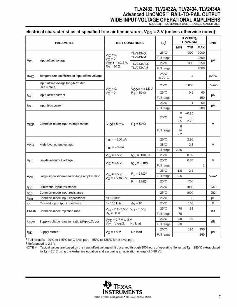
electrical characteristics at specified free-air temperature, VDD = 3 V (unless otherwise noted)
PARAMETER TEST CONDITIONS T †TLV243x
UNITPARAMETER TEST CONDITIONS TA†MIN TYP MAX
UNIT
VIC = 0 TLV243xC, 25°C 300 2000
VIO Input offset voltage
VIC = 0,VO = 0,
,TLV243xI Full range 2500
µVVIO Input offset voltage O ,VDD± = ±1.5 V,R 50 Ω TLV243xAI
25°C 300 950µV
RS = 50 Ω TLV243xAIFull range 1500
αVIO Temperature coefficient of input offset voltage25°C
2 µV/°CαVIO Temperature coefficient of input offset voltageto 70°C 2 µV/°C
Input offset voltage long-term drift(see Note 4) VIC = 0, VDD± = ±1.5 V,
25°C 0.003 µV/mo
IIO Input offset current
VIC = 0,VO = 0,
VDD± = ±1.5 V,RS = 50 Ω 25°C 0.5 60
pAIIO Input offset currentFull range 150
pA
IIB Input bias current25°C 1 60
pAIIB Input bias currentFull range 150
pA
VICR Common mode input voltage range |VIO| ≤ 5 mV RS = 50 Ω
25°C0to
2.5
–0.25to
2.75VVICR Common-mode input voltage range |VIO| ≤ 5 mV, RS = 50 Ω
Full range0to
2.2
V
IOH = –100 µA 25°C 2.98
VOH High-level output voltageIOH = 3 mA
25°C 2.5 VIOH = –3 mA
Full range 2.25
VIC = 1.5 V, IOL = 100 µA 25°C 0.02
VOL Low-level output voltageVIC = 1 5 V IOL = 3 A
25°C 0.83 VVIC = 1.5 V, IOL = 3 A
Full range 1
V 2 5 V R 2 kΩ‡25°C 1.5 2.5
AVD Large-signal differential voltage amplificationVIC = 2.5 V,VO = 1 V to 2 V
RL = 2 kهFull range 1 V/mVVD g g g VO = 1 V to 2 V
RL = 1 MΩ‡ 25°C 750
ri(d) Differential input resistance 25°C 1000 GΩ
ri(c) Common-mode input resistance 25°C 1000 GΩ
ci(c) Common-mode input capacitance f = 10 kHz 25°C 8 pF
zo Closed-loop output impedance f = 100 kHz, AV = 10 25°C 130 Ω
CMRR Common mode rejection ratioVIC = 0 to 2.5 V, VO = 1.5 V, 25°C 70 83
dBCMRR Common-mode rejection ratio IC , O ,RS = 50 Ω Full range 70
dB
kSVR Supply voltage rejection ratio (∆VDD/∆VIO)VDD = 2.7 V to 8 V, 25°C 80 95
dBkSVR Supply-voltage rejection ratio (∆VDD/∆VIO) DD ,VIC = VDD/2, No load Full range 80
dB
IDD Supply current (per channel) VO = 1 5 V No load25°C 98 125
µAIDD Supply current (per channel) VO = 1.5 V, No loadFull range 125
µA
† Full range for the C suffix is 0°C to 70°C. Full range for the dual I suffix is – 40°C to 85°C. Full range for the quad I suffix is – 40°C to 125°C.‡ Referenced to 2.5 VNOTE 4: Typical values are based on the input offset voltage shift observed through 500 hours of operating life test at TA = 150°C extrapolated
to TA = 25°C using the Arrhenius equation and assuming an activation energy of 0.96 eV.

TLV2432, TLV2432A, TLV2434, TLV2434AAdvanced LinCMOS RAIL-TO-RAIL OUTPUTWIDE-INPUT-VOLTAGE OPERATIONAL AMPLIFIERSSLOS168F – NOVEMBER 1996 – REVISED MARCH 2001
6 POST OFFICE BOX 655303 • DALLAS, TEXAS 75265
operating characteristics at specified free-air temperature, VDD = 3 V
PARAMETER TEST CONDITIONS T †TLV243x
UNITPARAMETER TEST CONDITIONS TA†MIN TYP MAX
UNIT
V 1 V t 2 V R 2 kΩ‡25°C 0.15 0.25
SR Slew rate at unity gain VO = 1 V to 2 V,CL = 100 pF‡
RL = 2 kه,Full
range0.1
V/µs
V Equivalent input noise voltagef = 10 Hz 25°C 120
nV/√HzVn Equivalent input noise voltagef = 1 kHz 25°C 22
nV/√Hz
VN(PP) Peak to peak equivalent input noise voltagef = 0.1 Hz to 1 Hz 25°C 2.7
µVVN(PP) Peak-to-peak equivalent input noise voltagef = 0.1 Hz to 10 Hz 25°C 4
µV
In Equivalent input noise current 25°C 0.6 fA√Hz
THD + N Total harmonic distortion plus noiseVO = 0.5 V to 2.5 V,f 1 kHz
AV = 125°C
0.065%THD + N Total harmonic distortion plus noise f = 1 kHz,
RL = 2 kΩ‡ AV = 1025°C
0.5%
Gain-bandwidth productf = 10 kHz, CL = 100 pF‡
RL = 2 kΩ‡, 25°C 0.5 MHz
BOM Maximum output-swing bandwidthVO(PP) = 1 V, RL = 2 kه,
AV = 1, CL = 100 pF‡ 25°C 220 kHz
AV = –1, To 0 1% 6 4
t Settling time
AV = 1,Step = 0.5 V to 2.5 V,
To 0.1%25°C
6.4µsts Settling time ,
RL = 2 kΩ‡,‡ To 0 01%
25°C14 1
µsL
CL = 100 pF‡ To 0.01% 14.1
φm Phase margin at unity gainRL = 2 kΩ‡ CL = 100 pF‡ 25°C 62°
Gain marginRL = 2 kΩ‡, CL = 100 pF‡
25°C 11 dB† Full range for the C suffix is 0°C to 70°C. Full range for the dual I suffix is – 40°C to 85°C. Full range for the quad I suffix is – 40°C to 125°C.‡ Referenced to 2.5 V
TLV2432, TLV2432A, TLV2434, TLV2434AAdvanced LinCMOS RAIL-TO-RAIL OUTPUT
WIDE-INPUT-VOLTAGE OPERATIONAL AMPLIFIERSSLOS168F – NOVEMBER 1996 – REVISED MARCH 2001
7POST OFFICE BOX 655303 • DALLAS, TEXAS 75265
electrical characteristics at specified free-air temperature, VDD = 3 V (unless otherwise noted)
PARAMETER TEST CONDITIONS TA†TLV243xQ,TLV243xM UNITA
MIN TYP MAX
VIC = 0 TLV243xQ, 25°C 300 2000
VIO Input offset voltage
VIC = 0,VO = 0,
,TLV243xM Full range 2500
µVVIO Input offset voltage O ,VDD± = ±1.5 V,R 50 Ω
TLV243xAQ, 25°C 300 950µV
RS = 50 Ω,
TLV243xAM Full range 2000
αVIO Temperature coefficient of input offset voltage25°C
2 µV/°CαVIO Temperature coefficient of input offset voltageto 70°C 2 µV/°C
Input offset voltage long-term drift(see Note 4) VIC = 0, VDD± = ±1.5 V,
25°C 0.003 µV/mo
IIO Input offset current
VIC = 0,VO = 0,
VDD± = ±1.5 V,RS = 50 Ω 25°C 0.5 60
pAIIO Input offset currentFull range 150
pA
IIB Input bias current25°C 1 60
pAIIB Input bias currentFull range 300
pA
VICR Common mode input voltage range |VIO| ≤ 5 mV RS = 50 Ω
25°C0to
2.5
–0.25to
2.75VVICR Common-mode input voltage range |VIO| ≤ 5 mV, RS = 50 Ω
Full range0to
2.2
V
IOH = –100 µA 25°C 2.98
VOH High-level output voltageIOH = 3 mA
25°C 2.5 VIOH = –3 mA
Full range 2.25
VIC = 1.5 V, IOL = 100 µA 25°C 0.02
VOL Low-level output voltageVIC = 1 5 V IOL = 3 A
25°C 0.83 VVIC = 1.5 V, IOL = 3 A
Full range 1
V 2 5 V R 2 kΩ‡25°C 1.5 2.5
AVD Large-signal differential voltage amplificationVIC = 2.5 V,VO = 1 V to 2 V
RL = 2 kهFull range 0.5 V/mVVD g g g VO = 1 V to 2 V
RL = 1 MΩ‡ 25°C 750
ri(d) Differential input resistance 25°C 1000 GΩ
ri(c) Common-mode input resistance 25°C 1000 GΩ
ci(c) Common-mode input capacitance f = 10 kHz 25°C 8 pF
zo Closed-loop output impedance f = 100 kHz, AV = 10 25°C 130 Ω
CMRR Common mode rejection ratioVIC = 0 to 2.5 V, VO = 1.5 V, 25°C 70 83
dBCMRR Common-mode rejection ratio IC , O ,RS = 50 Ω Full range 70
dB
kSVR Supply voltage rejection ratio (∆VDD/∆VIO)VDD = 2.7 V to 8 V, 25°C 80 95
dBkSVR Supply-voltage rejection ratio (∆VDD/∆VIO) DD ,VIC = VDD/2, No load Full range 80
dB
IDD Supply current VO = 1 5 V No load25°C 195 250
µAIDD Supply current VO = 1.5 V, No loadFull range 260
µA
† Full range is –40°C to 125°C for Q level part, –55°C to 125°C for M level part.‡ Referenced to 2.5 VNOTE 4: Typical values are based on the input offset voltage shift observed through 500 hours of operating life test at TA = 150°C extrapolated
to TA = 25°C using the Arrhenius equation and assuming an activation energy of 0.96 eV.

TLV2432, TLV2432A, TLV2434, TLV2434AAdvanced LinCMOS RAIL-TO-RAIL OUTPUTWIDE-INPUT-VOLTAGE OPERATIONAL AMPLIFIERSSLOS168F – NOVEMBER 1996 – REVISED MARCH 2001
8 POST OFFICE BOX 655303 • DALLAS, TEXAS 75265
operating characteristics at specified free-air temperature, VDD = 3 V
PARAMETER TEST CONDITIONS TA†
TLV243xQ,TLV243xM,
TLV243xAQ,TLV243xAM
UNIT
MIN TYP MAX
V 1 V t 2 V R 2 kΩ‡25°C 0.15 0.25
SR Slew rate at unity gain VO = 1 V to 2 V,CL = 100 pF‡
RL = 2 kه,Full
range0.1
V/µs
V Equivalent input noise voltagef = 10 Hz 25°C 120
nV/√HzVn Equivalent input noise voltagef = 1 kHz 25°C 22
nV/√Hz
VN(PP) Peak to peak equivalent input noise voltagef = 0.1 Hz to 1 Hz 25°C 2.7
µVVN(PP) Peak-to-peak equivalent input noise voltagef = 0.1 Hz to 10 Hz 25°C 4
µV
In Equivalent input noise current 25°C 0.6 fA√Hz
THD + N Total harmonic distortion plus noiseVO = 0.5 V to 2.5 V,f 1 kHz
AV = 125°C
0.065%THD + N Total harmonic distortion plus noise f = 1 kHz,
RL = 2 kΩ‡ AV = 1025°C
0.5%
Gain-bandwidth productf = 10 kHz, CL = 100 pF‡
RL = 2 kΩ‡, 25°C 0.5 MHz
BOM Maximum output-swing bandwidthVO(PP) = 1 V, RL = 2 kه,
AV = 1, CL = 100 pF‡ 25°C 220 kHz
AV = –1, To 0 1% 6 4
t Settling time
AV = 1,Step = 0.5 V to 2.5 V,
To 0.1%25°C
6.4µsts Settling time ,
RL = 2 kΩ‡,‡ To 0 01%
25°C14 1
µsL
CL = 100 pF‡ To 0.01% 14.1
φm Phase margin at unity gainRL = 2 kΩ‡ CL = 100 pF‡ 25°C 62°
Gain marginRL = 2 kΩ‡, CL = 100 pF‡
25°C 11 dB† Full range is –40°C to 125°C for Q level part, –55°C to 125°C for M level part.‡ Referenced to 2.5 V

TLV2432, TLV2432A, TLV2434, TLV2434AAdvanced LinCMOS RAIL-TO-RAIL OUTPUT
WIDE-INPUT-VOLTAGE OPERATIONAL AMPLIFIERSSLOS168F – NOVEMBER 1996 – REVISED MARCH 2001
9POST OFFICE BOX 655303 • DALLAS, TEXAS 75265
electrical characteristics at specified free-air temperature, VDD = 5 V (unless otherwise noted)
PARAMETER TEST CONDITIONS T †TLV243x
UNITPARAMETER TEST CONDITIONS TA†MIN TYP MAX
UNIT
VIC = 0 TLV243x25°C 300 2000
VIO Input offset voltage
VIC = 0,VO = 0,
TLV243xFull range 2500
µVVIO Input offset voltage O ,VDD± = ±2.5 V,R 50 Ω TLV243xA
25°C 300 950µV
RS = 50 Ω TLV243xAFull range 1500
αVIO Temperature coefficient of input offset voltage25°C
2 µV/°CαVIO Temperature coefficient of input offset voltageto 70°C 2 µV/°C
Input offset voltage long-term drift (see Note 4) VIC = 0, VDD± = ±2.5 V,
25°C 0.003 µV/mo
IIO Input offset current
VIC = 0,VO = 0,
VDD± = ±2.5 V,RS = 50 Ω 25°C 0.5 60
pAIIO Input offset currentFull range 150
pA
IIB Input bias current25°C 1 60
pAIIB Input bias currentFull range 150
pA
VICR Common mode input voltage range |VIO| ≤ 5 mV RS = 50 Ω
25°C0to
4.5
–0.25to
4.75VVICR Common-mode input voltage range |VIO| ≤ 5 mV, RS = 50 Ω
Full range0to
4.2
V
IOH = –100 µA 25°C 4.97
VOH High-level output voltageIOH = 5 mA
25°C 4 4.35 VIOH = –5 mA
Full range 4
VIC = 2.5 V, IOL = 100 µA 25°C 0.01
VOL Low-level output voltageVIC = 2 5 V IOL = 5 A
25°C 0.8 VVIC = 2.5 V, IOL = 5 A
Full range 1.25
V 2 5 V R 2 kΩ‡25°C 2.5 3.8
AVD Large-signal differential voltage amplificationVIC = 2.5 V,VO = 1 V to 4 V
RL = 2 kهFull range 1.5 V/mVVD g g g VO = 1 V to 4 V
RL = 1 MΩ‡ 25°C 950
ri(d) Differential input resistance 25°C 1000 GΩ
ri(c) Common-mode input resistance 25°C 1000 GΩ
ci(c) Common-mode input capacitance f = 10 kHz 25°C 8 pF
zo Closed-loop output impedance f = 100 kHz, AV = 10 25°C 130 Ω
CMRR Common mode rejection ratioVIC = 0 to 4.5 V, VO = 2.5 V, 25°C 70 90
dBCMRR Common-mode rejection ratio IC , O ,RS = 50 Ω Full range 70
dB
kSVR Supply voltage rejection ratio (∆VDD/∆VIO)VDD = 4.4 V to 8 V, 25°C 80 95
dBkSVR Supply-voltage rejection ratio (∆VDD/∆VIO) DD ,VIC = VDD/2, No load Full range 80
dB
IDD Supply current (per channel) VO = 2 5 V No load25°C 100 125
µAIDD Supply current (per channel) VO = 2.5 V, No loadFull range 125
µA
† Full range for the C suffix is 0°C to 70°C. Full range for the dual I suffix is – 40°C to 85°C. Full range for the quad I suffix is – 40°C to 125°C.‡ Referenced to 2.5 VNOTE 4: Typical values are based on the input offset voltage shift observed through 500 hours of operating life test at TA = 150°C extrapolated
to TA = 25°C using the Arrhenius equation and assuming an activation energy of 0.96 eV.

TLV2432, TLV2432A, TLV2434, TLV2434AAdvanced LinCMOS RAIL-TO-RAIL OUTPUTWIDE-INPUT-VOLTAGE OPERATIONAL AMPLIFIERSSLOS168F – NOVEMBER 1996 – REVISED MARCH 2001
10 POST OFFICE BOX 655303 • DALLAS, TEXAS 75265
operating characteristics at specified free-air temperature, VDD = 5 V
PARAMETER TEST CONDITIONS T †TLV243x
UNITPARAMETER TEST CONDITIONS TA†MIN TYP MAX
UNIT
VO 1 5 V to 3 5 V RL 2 kΩ‡25°C 0.15 0.25
SR Slew rate at unity gain VO = 1.5 V to 3.5 V,CL = 100 pF‡
RL = 2 kه,Full
0 1V/µs
CL = 100 F‡range
0.1
V Equivalent input noise voltagef = 10 Hz 25°C 100
nV/√HzVn Equivalent input noise voltagef = 1 kHz 25°C 18
nV/√Hz
VN(PP) Peak to peak equivalent input noise voltagef = 0.1 Hz to 1 Hz 25°C 1.9
µVVN(PP) Peak-to-peak equivalent input noise voltagef = 0.1 Hz to 10 Hz 25°C 2.8
µV
In Equivalent input noise current 25°C 0.6 fA√Hz
THD + N Total harmonic distortion plus noiseVO = 1.5 V to 3.5 V,f 1 kHz
AV = 125°C
0.045%THD + N Total harmonic distortion plus noise f = 1 kHz,
RL = 2 kΩ‡ AV = 1025°C
0.4%
Gain-bandwidth productf = 10 kHz, CL = 100 pF‡
RL =2 kΩ‡, 25°C 0.55 MHz
BOM Maximum output-swing bandwidthVO(PP) = 2 V, RL = 2 kه,
AV = 1, CL = 100 pF‡ 25°C 100 kHz
AV = –1, To 0 1% 6 4t Settling time
AV = 1,Step = 1.5 V to 3.5 V,
To 0.1%25°C
6.4µsts Settling time ,
RL = 2 kΩ‡,‡ To 0 01%
25°C13 1
µsL
CL = 100 pF‡ To 0.01% 13.1
φm Phase margin at unity gainRL = 2 kΩ‡ CL = 100 pF‡ 25°C 66°
Gain marginRL = 2 kΩ‡, CL = 100 pF‡
25°C 11 dB† Full range for the C suffix is 0°C to 70°C. Full range for the dual I suffix is – 40°C to 85°C. Full range for the quad I suffix is – 40°C to 125°C.‡ Referenced to 2.5 V

TLV2432, TLV2432A, TLV2434, TLV2434AAdvanced LinCMOS RAIL-TO-RAIL OUTPUT
WIDE-INPUT-VOLTAGE OPERATIONAL AMPLIFIERSSLOS168F – NOVEMBER 1996 – REVISED MARCH 2001
11POST OFFICE BOX 655303 • DALLAS, TEXAS 75265
electrical characteristics at specified free-air temperature, VDD = 5 V (unless otherwise noted)
PARAMETER TEST CONDITIONS TA†TLV243xQ,TLV243xM UNITA
MIN TYP MAX
VIC = 0 TLV2453x25°C 300 2000
VIO Input offset voltage
VIC = 0,VO = 0,
TLV2453xFull range 2500
µVVIO Input offset voltage O ,VDD± = ±2.5 V,R 50 Ω TLV2453xA
25°C 300 950µV
RS = 50 Ω TLV2453xAFull range 2000
αVIO Temperature coefficient of input offset voltage25°C
2 µV/°CαVIO Temperature coefficient of input offset voltageto 70°C 2 µV/°C
Input offset voltage long-term drift (see Note 4) VIC = 0, VDD± = ±2.5 V,
25°C 0.003 µV/mo
IIO Input offset current
VIC = 0,VO = 0,
VDD± = ±2.5 V,RS = 50 Ω 25°C 0.5 60
pAIIO Input offset currentFull range 150
pA
IIB Input bias current25°C 1 60
pAIIB Input bias currentFull range 300
pA
VICR Common mode input voltage range |VIO| ≤ 5 mV RS = 50 Ω
25°C0to
4.5
–0.25to
4.75VVICR Common-mode input voltage range |VIO| ≤ 5 mV, RS = 50 Ω
Full range0to
4.2
V
IOH = –100 µA 25°C 4.97
VOH High-level output voltageIOH = 5 mA
25°C 4 4.35 VIOH = –5 mA
Full range 4
VIC = 2.5 V, IOL = 100 µA 25°C 0.01
VOL Low-level output voltageVIC = 2 5 V IOL = 5 A
25°C 0.8 VVIC = 2.5 V, IOL = 5 A
Full range 1.25
V 2 5 V R 2 kΩ‡25°C 2.5 3.8
AVD Large-signal differential voltage amplificationVIC = 2.5 V,VO = 1 V to 4 V
RL = 2 kهFull range 0.5 V/mVVD g g g VO = 1 V to 4 V
RL = 1 MΩ‡ 25°C 950
ri(d) Differential input resistance 25°C 1000 GΩ
ri(c) Common-mode input resistance 25°C 1000 GΩ
ci(c) Common-mode input capacitance f = 10 kHz 25°C 8 pF
zo Closed-loop output impedance f = 100 kHz, AV = 10 25°C 130 Ω
CMRR Common mode rejection ratioVIC = 0 to 4.5 V, VO = 2.5 V, 25°C 70 90
dBCMRR Common-mode rejection ratio IC , O ,RS = 50 Ω Full range 70
dB
kSVR Supply voltage rejection ratio (∆VDD/∆VIO)VDD = 4.4 V to 8 V, 25°C 80 95
dBkSVR Supply-voltage rejection ratio (∆VDD/∆VIO) DD ,VIC = VDD/2, No load Full range 80
dB
IDD Supply current VO = 2 5 V No load25°C 200 250
µAIDD Supply current VO = 2.5 V, No loadFull range 270
µA
† Full range is –40°C to 125°C for Q level part, –55°C to 125°C for M level part.‡ Referenced to 2.5 VNOTE 4: Typical values are based on the input offset voltage shift observed through 500 hours of operating life test at TA = 150°C extrapolated
to TA = 25°C using the Arrhenius equation and assuming an activation energy of 0.96 eV.

TLV2432, TLV2432A, TLV2434, TLV2434AAdvanced LinCMOS RAIL-TO-RAIL OUTPUTWIDE-INPUT-VOLTAGE OPERATIONAL AMPLIFIERSSLOS168F – NOVEMBER 1996 – REVISED MARCH 2001
12 POST OFFICE BOX 655303 • DALLAS, TEXAS 75265
operating characteristics at specified free-air temperature, VDD = 5 V
PARAMETER TEST CONDITIONS TA†
TLV243xQ,TLV243xM,
TLV243xAQ,TLV243xAM
UNIT
MIN TYP MAX
VO 1 5 V to 3 5 V RL 2 kΩ‡25°C 0.15 0.25
SR Slew rate at unity gain VO = 1.5 V to 3.5 V,CL = 100 pF‡
RL = 2 kه,Full
0 1V/µs
CL = 100 F‡range
0.1
V Equivalent input noise voltagef = 10 Hz 25°C 100
nV/√HzVn Equivalent input noise voltagef = 1 kHz 25°C 18
nV/√Hz
VN(PP) Peak to peak equivalent input noise voltagef = 0.1 Hz to 1 Hz 25°C 1.9
µVVN(PP) Peak-to-peak equivalent input noise voltagef = 0.1 Hz to 10 Hz 25°C 2.8
µV
In Equivalent input noise current 25°C 0.6 fA√Hz
THD + N Total harmonic distortion plus noiseVO = 1.5 V to 3.5 V,f 1 kHz
AV = 125°C
0.045%THD + N Total harmonic distortion plus noise f = 1 kHz,
RL = 2 kΩ‡ AV = 1025°C
0.4%
Gain-bandwidth productf = 10 kHz, CL = 100 pF‡
RL =2 kΩ‡, 25°C 0.55 MHz
BOM Maximum output-swing bandwidthVO(PP) = 2 V, RL = 2 kه,
AV = 1, CL = 100 pF‡ 25°C 100 kHz
AV = –1, To 0 1% 6 4
t Settling time
AV = 1,Step = 1.5 V to 3.5 V,
To 0.1%25°C
6.4µsts Settling time ,
RL = 2 kΩ‡,‡ To 0 01%
25°C13 1
µsL
CL = 100 pF‡ To 0.01% 13.1
φm Phase margin at unity gainRL = 2 kΩ‡ CL = 100 pF‡ 25°C 66°
Gain marginRL = 2 kΩ‡, CL = 100 pF‡
25°C 11 dB† Full range is –40°C to 125°C for Q level part, –55°C to 125°C for M level part.‡ Referenced to 2.5 V

TLV2432, TLV2432A, TLV2434, TLV2434AAdvanced LinCMOS RAIL-TO-RAIL OUTPUT
WIDE-INPUT-VOLTAGE OPERATIONAL AMPLIFIERSSLOS168F – NOVEMBER 1996 – REVISED MARCH 2001
13POST OFFICE BOX 655303 • DALLAS, TEXAS 75265
TYPICAL CHARACTERISTICS
Table of GraphsFIGURE
VIO Input offset voltageDistribution 2,3
VIO Input offset voltagevs Common-mode input voltage
,4,5
αVIO Temperature coefficient Distribution 6,7
IIB/IIO Input bias and input offset currents vs Free-air temperature 8
VOH High-level output voltage vs High-level output current 9,11
VOL Low-level output voltage vs Low-level output current 10,12
VO(PP) Maximum peak-to-peak output voltage vs Frequency 13
IOS Short circuit output currentvs Supply voltage 14
IOS Short-circuit output currenty g
vs Free-air temperature 15
VID Differential input voltage vs Output voltage 16,17
Differential gain vs Load resistance 18
AVD Large-signal differential voltage amplification vs Frequency 19,20
AVD Differential voltage amplification vs Free-air temperature 21,22
zo Output impedance vs Frequency 23,24
CMRR Common mode rejection ratiovs Frequency 25
CMRR Common-mode rejection ratioq y
vs Free-air temperature 26
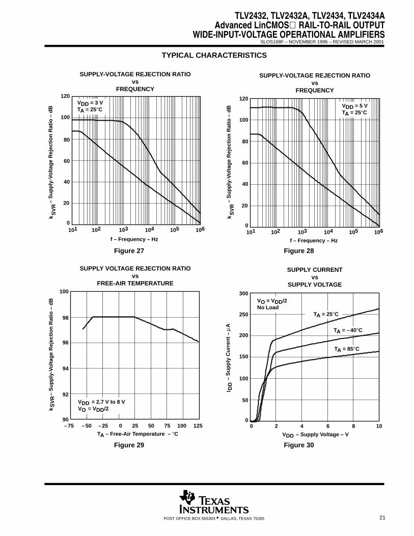
kSVR Supply voltage rejection ratiovs Frequency 27,28
kSVR Supply-voltage rejection ratioq y
vs Free-air temperature,
29
IDD Supply current vs Supply voltage 30
SR Slew ratevs Load capacitance 31
SR Slew ratevs Free-air temperature 32
VO Inverting large-signal pulse response 33,34
VO Voltage-follower large-signal pulse response 35,36
VO Inverting small-signal pulse response 37,38
VO Voltage-follower small-signal pulse response 39,40
Vn Equivalent input noise voltage vs Frequency 41, 42
Noise voltage (referred to input) Over a 10-second period 43
THD + N Total harmonic distortion plus noise vs Frequency 44,45
Gain bandwidth productvs Free-air temperature 46
Gain-bandwidth productvs Supply voltage 47
φ Phase marginvs Frequency 19,20φm Phase margin
q yvs Load capacitance
,48
Gain margin vs Load capacitance 49
B1 Unity-gain bandwidth vs Load capacitance 50

TLV2432, TLV2432A, TLV2434, TLV2434AAdvanced LinCMOS RAIL-TO-RAIL OUTPUTWIDE-INPUT-VOLTAGE OPERATIONAL AMPLIFIERSSLOS168F – NOVEMBER 1996 – REVISED MARCH 2001
14 POST OFFICE BOX 655303 • DALLAS, TEXAS 75265
TYPICAL CHARACTERISTICS
Figure 2
15
5
0–1600 –800 0
25
30
35
800 1600
20
10
408 Amplifiers From 1 Wafer LotVDD± = ± 1.5 VTA = 25°C
Pre
cen
tag
e o
f Am
plif
iers
– %
DISTRIBUTION OF TLV2432INPUT OFFSET VOLTAGE
VIO – Input Offset Voltage – µV
Figure 3
20
15
5
0–1600 –800 0
25
30
35
800 1600
10
408 Amplifiers From 1 Wafer Lot
Per
cen
tag
e o
f Am
plif
iers
– %
DISTRIBUTION OF TLV2432INPUT OFFSET VOLTAGE
VIO – Input Offset Voltage – µV
VDD± = ± 2.5 VTA = 25°C
Figure 4
0
–0.5
–1.5
–2–0.5 0 0.5 1 1.5
1
1.5
2
2 2.5 3
0.5
–1
VDD =3 VTA = 25°C
VIO
– In
pu
t O
ffse
t V
olt
age
– m
V
INPUT OFFSET VOLTAGEvs
COMMON-MODE INPUT VOLTAGE
ÁÁÁÁÁÁÁÁÁ
VIO
VIC – Common-Mode Input Voltage – V
Figure 5
0
–0.5
–1.5
–2–0.5 0 0.5 1 1.5 2 2.5
1
1.5
2
3 3.5 4 5
0.5
–1
4.5
VDD = 5 VTA = 25°C
VIO
– In
pu
t O
ffse
t V
olt
age
– m
V
INPUT OFFSET VOLTAGEvs
COMMON-MODE INPUT VOLTAGE
ÁÁÁÁÁÁ
VIO
VIC – Common-Mode Input Voltage – V

TLV2432, TLV2432A, TLV2434, TLV2434AAdvanced LinCMOS RAIL-TO-RAIL OUTPUT
WIDE-INPUT-VOLTAGE OPERATIONAL AMPLIFIERSSLOS168F – NOVEMBER 1996 – REVISED MARCH 2001
15POST OFFICE BOX 655303 • DALLAS, TEXAS 75265
TYPICAL CHARACTERISTICS
Figure 6
10
5
0–4 –3 –2 –1 0 1
15
20
25
2 3 4
32 Amplifiers From 1 Wafer LotVDD = ± 1.5 VTA = 25°C to 125°C
Per
cen
tag
e o
f Am
plif
iers
– %
DISTRIBUTION OF TLV2432 INPUT OFFSETVOLTAGE TEMPERATURE COEFFICIENT
αVIO – Temperature Coefficient – µV/ °C
Figure 7
10
5
0–4 –3 –2 –1 0 1
15
20
25
2 3 4
32 Amplifiers From 1 Wafer LotVDD = ± 2.5 VTA = 25°C to 125°C
Per
cen
tag
e o
f Am
plif
iers
– %
DISTRIBUTION OF TLV2432 INPUT OFFSETVOLTAGE TEMPERATURE COEFFICIENT
αVIO – Temperature Coefficient – µV/ °C
Figure 8
10
5
30
025 45 65 85IIB
an
d II
O –
Inp
ut
Bia
s an
d In
pu
t O
ffse
t C
urr
ents
– p
A
20
15
25
INPUT BIAS AND INPUT OFFSET CURRENTSvs
FREE-AIR TEMPERATURE35
105 125
IIB
IIO
VDD± = ±2.5 VVIC = 0 VVO = 0RS = 50 Ω
TA – Free-Air Temperature – °C
ÁÁÁÁ
I IBI IO
Figure 9
TA = –40°C
TA = 25°C
TA = 0°C
TA = 125°C
VDD = 3 V
1.5
1
0.5
00 3 6 9
2
2.5
3
12 15
VO
H –
Hig
h-L
evel
Ou
tpu
t V
olt
age
– V
HIGH-LEVEL OUTPUT VOLTAGEvs
HIGH-LEVEL OUTPUT CURRENT
IOH – High-Level Output Current – mA
ÁÁÁÁ
V OH

TLV2432, TLV2432A, TLV2434, TLV2434AAdvanced LinCMOS RAIL-TO-RAIL OUTPUTWIDE-INPUT-VOLTAGE OPERATIONAL AMPLIFIERSSLOS168F – NOVEMBER 1996 – REVISED MARCH 2001
16 POST OFFICE BOX 655303 • DALLAS, TEXAS 75265
TYPICAL CHARACTERISTICS
Figure 10
TA = 125°C
1.4
4 5
TA = 85°C
TA = 25°C
TA = –40°C
VDD = 3 V
0.8
0.6
0.2
00 1 2 3
1
1.2
0.4
VO
L –
Lo
w-L
evel
Ou
tpu
t V
olt
age
– V
LOW-LEVEL OUTPUT VOLTAGEvs
LOW-LEVEL OUTPUT CURRENT
IOL – Low-Level Output Current – mA
ÁÁÁÁÁÁ
V OL
Figure 11
TA = 125°C
TA = 85°C
TA = 25°C
TA =–40°C
VDD = 5 V
2
1
00 4 8 12
3
4
5
16 20
VO
H –
Hig
h-L
evel
Ou
tpu
t V
olt
age
– V
HIGH-LEVEL OUTPUT VOLTAGEvs
HIGH-LEVEL OUTPUT CURRENT
IOH – High-Level Output Current – A
ÁÁÁÁ
V OH
Figure 12
TA = 125°C
TA = 85°C
TA = 25°C
TA = –40°C
VDD = 5 V
0.6
0.4
0.2
00 1 2 3
0.8
1
1.2
4 5
VO
L –
Lo
w-L
evel
Ou
tpu
t V
olt
age
– V
LOW-LEVEL OUTPUT VOLTAGEvs
LOW-LEVEL OUTPUT CURRENT
ÁÁÁÁÁÁÁÁÁ
V OL
IOL – Low-Level Output Current – mA
Figure 13
4
2
1
0
5
3
102 103 104 105 106
VDD = 5 V
VDD = 3 V
RL = 2 kΩTA = 25°C
VO
(PP
) –
Max
imu
m P
eak-
to-P
eak
Ou
tpu
t V
olt
age
– V
f – Frequency – Hz
MAXIMUM PEAK-TO-PEAK OUTPUT VOLTAGEvs
FREQUENCY
ÁÁÁÁÁÁV
O(P
P)

TLV2432, TLV2432A, TLV2434, TLV2434AAdvanced LinCMOS RAIL-TO-RAIL OUTPUT
WIDE-INPUT-VOLTAGE OPERATIONAL AMPLIFIERSSLOS168F – NOVEMBER 1996 – REVISED MARCH 2001
17POST OFFICE BOX 655303 • DALLAS, TEXAS 75265
TYPICAL CHARACTERISTICS
Figure 14
VO = VDD/2VIC = VDD/2TA = 25°C
0
–5
–15
–202 3 4 5 6 7
10
15
20
8 9 10
5
–10
IOS
– S
ho
rt-C
ircu
it O
utp
ut
Cu
rren
t –
mA
SHORT-CIRCUIT OUTPUT CURRENTvs
SUPPLY VOLTAGE
I OS
VDD – Supply Voltage – V
Figure 15
0
–5
–15
–20–75 –50 –25 0 25 50
10
15
20
75 100 125
5
–10
VID = –100 mV
VID = 100 mV
VDD = 5 VVIC = 2.5 VVO = 2.5 V
IOS
– S
ho
rt-C
ircu
it O
utp
ut
Cu
rren
t –
mA
SHORT-CIRCUIT OUTPUT CURRENTvs
FREE-AIR TEMPERATURE
TA – Free-Air Temperature – °C
I OS
Figure 16
VO – Output Voltage – V
VDD = 3 VRL = 2 kΩVIC = 1.5 VTA = 25°C
0
–250
–500
–10000 0.5 1 1.5
– D
iffe
ren
tial
Inp
ut
Vo
ltag
e – 500
750
DIFFERENTIAL INPUT VOLTAGEvs
OUTPUT VOLTAGE1000
2 2.5 3
250
–750VID
Vµ
Figure 17
VDD = 5 VVIC = 2.5 VRL = 2 kΩTA = 25°C
0
–250
–750
–10000 1 2 3
500
750
DIFFERENTIAL INPUT VOLTAGEvs
OUTPUT VOLTAGE1000
4 5
VO – Output Voltage – V
– D
iffe
ren
tial
Inp
ut
Vo
ltag
e –
VID
Vµ
250
–500

TLV2432, TLV2432A, TLV2434, TLV2434AAdvanced LinCMOS RAIL-TO-RAIL OUTPUTWIDE-INPUT-VOLTAGE OPERATIONAL AMPLIFIERSSLOS168F – NOVEMBER 1996 – REVISED MARCH 2001
18 POST OFFICE BOX 655303 • DALLAS, TEXAS 75265
TYPICAL CHARACTERISTICS
VDD = 5 V
VDD = 3 V
VO(PP) = 2 VTA = 25°C
1
Dif
fere
nti
al G
ain
– V
/ mV
DIFFERENTIAL GAINvs
LOAD RESISTANCE
RL – Load Resistance – kΩ
103
102
101
1 101 102 103
Figure 18
104
VDD = 5 VRL = 2 kΩCL = 100 pFTA = 25°C
40
20
0
–40
80
–20
60
105 106 107
om
– P
has
e M
arg
in
φ m
f – Frequency – Hz
LARGE-SIGNAL DIFFERENTIAL VOLTAGEAMPLIFICATION AND PHASE MARGIN
vsFREQUENCY
AV
D –
Lar
ge-
Sig
nal
Dif
fere
nti
al
ÁÁÁÁ
AV
D Vo
ltag
e A
mp
lific
atio
n –
dB
180°
135°
90°
45°
0°
–45°
–90°
Figure 19

TLV2432, TLV2432A, TLV2434, TLV2434AAdvanced LinCMOS RAIL-TO-RAIL OUTPUT
WIDE-INPUT-VOLTAGE OPERATIONAL AMPLIFIERSSLOS168F – NOVEMBER 1996 – REVISED MARCH 2001
19POST OFFICE BOX 655303 • DALLAS, TEXAS 75265
TYPICAL CHARACTERISTICS
40
20
0
–40
80
–20
60
VDD = 3 VRL = 2 kΩCL = 100 pFTA = 25°C
om
– P
has
e M
arg
in
φ m
f – Frequency – Hz
LARGE-SIGNAL DIFFERENTIAL VOLTAGEAMPLIFICATION AND PHASE MARGIN
vsFREQUENCY
AV
D –
Lar
ge-
Sig
nal
Dif
fere
nti
al
ÁÁÁÁÁÁ
AV
D Vo
ltag
e A
mp
lific
atio
n –
dB
104 105 106 107
180°
135°
90°
45°
0°
–45°
–90°
Figure 20
Figure 21
10
1
0.1
1000
100
– D
iffe
ren
tial
Vo
ltag
e A
mp
lific
atio
n –
V/m
VA
VD
TA – Free-Air Temperature – °C–75 –50 –25 0 25 50 75 100 125
10000
VDD = 5 V VIC = 2.5 VVO = 1 V to 4 V
RL = 1 MΩ
RL = 2 kΩ
DIFFERENTIAL VOLTAGE AMPLIFICATIONvs
FREE-AIR TEMPERATURE
Figure 22
10
1
0.1
1000
100
– D
iffe
ren
tial
Vo
ltag
e A
mp
lific
atio
n –
V/m
VA
VD
DIFFERENTIAL VOLTAGE AMPLIFICATIONvs
FREE-AIR TEMPERATURE
TA – Free-Air Temperature – °C–75 –50 –25 0 25 50 75 100 125
VDD = 3 V VIC = 2.5 VVO = 0.5 V to 2.5 V
RL = 1 MΩ
RL = 2 kΩ

TLV2432, TLV2432A, TLV2434, TLV2434AAdvanced LinCMOS RAIL-TO-RAIL OUTPUTWIDE-INPUT-VOLTAGE OPERATIONAL AMPLIFIERSSLOS168F – NOVEMBER 1996 – REVISED MARCH 2001
20 POST OFFICE BOX 655303 • DALLAS, TEXAS 75265
TYPICAL CHARACTERISTICS
Figure 23
102
AV = 100
AV = 10
AV = 1
VDD = 3 VTA = 25°C
100
10
1
1000
103 104 105
zo –
Ou
tpu
t Im
ped
ance
– 0
OUTPUT IMPEDANCEvs
FREQUENCY
f – Frequency – Hz
Ωz o
Figure 24
102
AV = 100
AV = 10
AV = 1
VDD = 5 VTA = 25°C
100
10
1
1000
103 104 105
OUTPUT IMPEDANCEvs
FREQUENCY
f – Frequency – Hz
zo –
Ou
tpu
t Im
ped
ance
– 0Ω
z o
Figure 25
102
80
40
20
0
100
60
103 104 105 106
VDD = 5 VVIC = 2.5 V
VDD = 3 VVIC = 1.5 V
TA = 25°C
f – Frequency – Hz
COMMON-MODE REJECTION RATIOvs
FREQUENCY
CM
RR
– C
om
mo
n-M
od
e R
ejec
tio
n R
atio
– d
B
Figure 26
TA – Free-Air Temperature – °C
CM
RR
– C
om
mo
n-M
od
e R
ejec
tio
n R
atio
– d
B
COMMON-MODE REJECTION RATIOvs
FREE-AIR TEMPERATURE
–75 –50 –25 0 25 50 75 100 125
VDD = 5 V
VDD = 3 V
96
94
92
90
100
98
TLV2432, TLV2432A, TLV2434, TLV2434AAdvanced LinCMOS RAIL-TO-RAIL OUTPUT
WIDE-INPUT-VOLTAGE OPERATIONAL AMPLIFIERSSLOS168F – NOVEMBER 1996 – REVISED MARCH 2001
21POST OFFICE BOX 655303 • DALLAS, TEXAS 75265
TYPICAL CHARACTERISTICS
Figure 27
101
80
60
40
0
120
20
100
102 103 104 105 106
VDD = 3 VTA = 25°C
f – Frequency – Hz
SUPPLY-VOLTAGE REJECTION RATIOvs
FREQUENCY
KS
VR
– S
up
ply
-Vo
ltag
e R
ejec
tio
n R
atio
– d
B
ÁÁÁÁÁÁ
kS
VR
Figure 28
101
80
60
40
0
120
20
100
102 103 104 105 106
VDD = 5 VTA = 25°C
KS
VR
– S
up
ply
-Vo
ltag
e R
ejec
tio
n R
atio
– d
B
f – Frequency – Hz
SUPPLY-VOLTAGE REJECTION RATIOvs
FREQUENCY
ÁÁÁÁÁÁ
kS
VR
Figure 29
TA – Free-Air Temperature – °C
SUPPLY VOLTAGE REJECTION RATIOvs
FREE-AIR TEMPERATURE
96
94
92
90
100
–75 –50 –25 0 25 50 75 100 125
VDD = 2.7 V to 8 VVO = VDD/2
98
kSV
R –
Su
pp
ly-V
olt
age
Rej
ecti
on
Rat
io –
dB
kS
VR
Figure 30
150
100
50
00 2 4 6
200
250
300
8 10
VO = VDD/2No Load
TA = 25°C
TA = –40°C
TA = 85°C
IDD
– S
up
ply
Cu
rren
t –
SUPPLY CURRENTvs
SUPPLY VOLTAGE
VDD – Supply Voltage – V
ÁÁÁÁÁÁ
I DD
Aµ

TLV2432, TLV2432A, TLV2434, TLV2434AAdvanced LinCMOS RAIL-TO-RAIL OUTPUTWIDE-INPUT-VOLTAGE OPERATIONAL AMPLIFIERSSLOS168F – NOVEMBER 1996 – REVISED MARCH 2001
22 POST OFFICE BOX 655303 • DALLAS, TEXAS 75265
TYPICAL CHARACTERISTICS
Figure 31
101
SR+
VDD = 3 VAV = –1TA = 25°C
SR–
0.4
0.3
0.2
0
0.6
0.1
0.5
SR
– S
lew
Rat
e –
v/u
s
SLEW RATEvs
LOAD CAPACITANCE
sµ
V/
CL – Load Capacitance – pF102 103 104 105
Figure 32
TA – Free-Air Temperature – °C
SLEW RATEvs
FREE-AIR TEMPERATURE
0.25
0.2
0.15
0.1
0.35
–75 –50 –25 0 25 50 75 100 125
0.3
VDD = 5 VRL = 2 kΩCL = 100 pFAV = 1
µs
SR
– S
lew
Rat
e –
V/
Figure 33
1.5
1
0.5
00 10 20 30
2
2.5
3
40 50
INVERTING LARGE-SIGNAL PULSERESPONSE
VDD = 3 VRL = 2 kΩCL = 100 pFAV = –1TA = 25°C
t – Time – µs
VO
– O
utp
ut
Vo
ltag
e –
VV
O
Figure 34
INVERTING LARGE-SIGNAL PULSERESPONSE
VDD = 5 VRL = 2 kΩCL = 100 pFAV = –1TA = 25°C
t – Time – µs
2
1
00 10 20 30
3
4
5
40 50
VO
– O
utp
ut
Vo
ltag
e –
VV
O
TLV2432, TLV2432A, TLV2434, TLV2434AAdvanced LinCMOS RAIL-TO-RAIL OUTPUT
WIDE-INPUT-VOLTAGE OPERATIONAL AMPLIFIERSSLOS168F – NOVEMBER 1996 – REVISED MARCH 2001
23POST OFFICE BOX 655303 • DALLAS, TEXAS 75265
TYPICAL CHARACTERISTICS
Figure 35
1.5
1
0.5
00 10 20 30
2
2.5
3
40 50
VOLTAGE-FOLLOWER LARGE-SIGNALPULSE RESPONSE
VDD = 3 VRL = 2 kΩCL = 100 pFAV = 1TA = 25°C
t – Time – µs
VO
– O
utp
ut
Vo
ltag
e –
VV
O
Figure 36
VOLTAGE-FOLLOWER LARGE-SIGNALPULSE RESPONSE
VDD = 5 VRL = 2 kΩCL = 100 pFAV = 1TA = 25°C
t – Time – µsV
O –
Ou
tpu
t V
olt
age
– V
VO
2
1
00 5 10 15 20 25 30
3
4
5
35 40 45 50
Figure 37
1.5
1.48
1.46
1.440 0.5 1 1.5 2 2.5 3
1.52
1.56
1.58
3.5 4 4.5 5
VDD = 3 VRL = 2 kΩCL = 100 pFAV = –1TA = 25°C
t – Time – µs
VO
– O
utp
ut
Vo
ltag
e –
V
INVERTING SMALL-SIGNAL PULSERESPONSE
1.54
VO
Figure 38
2.48
2.46
2.440 0.5 1 1.5 2 2.5 3
2.54
2.56
2.58
3.5 4 4.5 5
INVERTING SMALL-SIGNALPULSE RESPONSE
VDD = 5 VRL = 2 kΩCL = 100 pFAV = –1TA = 25°C
VO
– O
utp
ut
Vo
ltag
e –
VV
O
t – Time – µs
2.52
2.5

TLV2432, TLV2432A, TLV2434, TLV2434AAdvanced LinCMOS RAIL-TO-RAIL OUTPUTWIDE-INPUT-VOLTAGE OPERATIONAL AMPLIFIERSSLOS168F – NOVEMBER 1996 – REVISED MARCH 2001
24 POST OFFICE BOX 655303 • DALLAS, TEXAS 75265
TYPICAL CHARACTERISTICS
Figure 39
1.5
1.48
1.46
1.440 0.5 1 1.5 2 2.5 3
1.54
1.56
1.58
3.5 4 4.5 5
VOLTAGE-FOLLOWER SMALL-SIGNALPULSE RESPONSE
VDD = 3 VRL = 2 kΩCL = 100 pFAV = 1TA = 25°C
VO
– O
utp
ut
Vo
ltag
e –
VV
O
t – Time – µs
1.52
Figure 40
2.5
2.46
2.440 0.5 1 1.5 2 2.5 3
2.52
2.56
2.58
3.5 4 4.5 5
VOLTAGE-FOLLOWER SMALL-SIGNALPULSE RESPONSE
t – Time – µs
VO
– O
utp
ut
Vo
ltag
e –
VV
O
VDD = 5 VRL = 2 kΩCL = 100 pFAV = 1TA = 25°C2.54
2.48
Figure 41
101
80
60
20
0
120
40
100
VN
– E
qu
ival
ent
Inp
ut
No
ise
Vo
ltag
e –
nv/
/Hz
f – Frequency – Hz
EQUIVALENT INPUT NOISE VOLTAGEvs
FREQUENCY
nV
/H
zV
n
VDD = 3 VRS = 20 ΩTA = 25°C
102 103 104
Figure 42
101
80
60
20
0
120
40
100
VN
– E
qu
ival
ent
Inp
ut
No
ise
Vo
ltag
e –
nv/
/Hz
f – Frequency – Hz
EQUIVALENT INPUT NOISE VOLTAGEvs
FREQUENCY
nV
/H
zV
n
VDD = 5 VRS = 20 ΩTA = 25°C
102 103 104

TLV2432, TLV2432A, TLV2434, TLV2434AAdvanced LinCMOS RAIL-TO-RAIL OUTPUT
WIDE-INPUT-VOLTAGE OPERATIONAL AMPLIFIERSSLOS168F – NOVEMBER 1996 – REVISED MARCH 2001
25POST OFFICE BOX 655303 • DALLAS, TEXAS 75265
TYPICAL CHARACTERISTICS
0
–500
–1500
–20000 1 2 3 4 5 6
500
1500
2000
7 8 9 10
No
ise
Vo
ltag
e –
nV
t – Time – s
NOISE VOLTAGE OVER A 10-SECOND PERIOD
VDD = 5 Vf = 0.1 Hz to 10 HzTA = 25°C
1000
–1000
Figure 43
Figure 44
101
1
0.1
0.01
10
TH
D +
N –
To
tal H
arm
on
ic D
isto
rtio
n P
lus
No
ise
– %
f – Frequency – Hz
TOTAL HARMONIC DISTORTION PLUS NOISEvs
FREQUENCY
AV = 10
AV = 1
VDD = 5 VTA = 25°C
AV = 10AV = 1
RL = 2 kΩ Tied to 2.5 VRL = 2 kΩ Tied to 0 V
102 103 104 105
Figure 45
101
TH
D +
N –
To
tal H
arm
on
ic D
isto
rtio
n P
lus
No
ise
– %
f – Frequency – Hz
TOTAL HARMONIC DISTORTION PLUS NOISEvs
FREQUENCY
AV = 10
AV = 1
VDD = 3 VTA = 25°C
AV = 10
AV = 1
RL = 2 kΩ Tied to 1.5 VRL = 2 kΩ Tied to 0 V
1
0.1
0.01
10
102 103 104 105

TLV2432, TLV2432A, TLV2434, TLV2434AAdvanced LinCMOS RAIL-TO-RAIL OUTPUTWIDE-INPUT-VOLTAGE OPERATIONAL AMPLIFIERSSLOS168F – NOVEMBER 1996 – REVISED MARCH 2001
26 POST OFFICE BOX 655303 • DALLAS, TEXAS 75265
TYPICAL CHARACTERISTICS
Figure 46
400
300
100
0–50 –25 0 25 50
500
700
800
75 100 125
Gai
n-B
and
wid
th P
rod
uct
– k
Hz
GAIN-BANDWIDTH PRODUCTvs
FREE-AIR TEMPERATURE
TA – Free-Air Temperature – °C
RL = 2 kΩCL = 100 pFf = 10 kHz
600
200
Figure 47
600
550
5000 1 2 3 4
650
700
750
5 6 7 8
Gai
n-B
and
wid
th P
rod
uct
– k
Hz
GAIN-BANDWIDTH PRODUCTvs
SUPPLY VOLTAGE
VDD – Supply Voltage – V
f = 10 kHzRL = 2 kΩCL = 100 pFTA = 25°C
Figure 48
101
75°
om
– P
has
e M
arg
in
PHASE MARGINvs
LOAD CAPACITANCE
CL – Load Capacitance – pF
mφ
Rnull = 500 ΩRnull = 1000 Ω
Rnull = 0
Rnull = 100 Ω
TA = 25°CRL = 2 kΩ
Rnull = 200 Ω
60°
45°
30°
15°
0°102 103 104 105
Figure 49
101
15
10
5
0
20
Gai
n M
arg
in –
dB
GAIN MARGINvs
LOAD CAPACITANCE
CL – Load Capacitance – pF
TA = 25°CRL = 2 kΩ
Rnull = 200 Ω
Rnull = 0
Rnull = 100 Ω
Rnull = 500 Ω
Rnull = 1 kΩ
102 103 104 105

TLV2432, TLV2432A, TLV2434, TLV2434AAdvanced LinCMOS RAIL-TO-RAIL OUTPUT
WIDE-INPUT-VOLTAGE OPERATIONAL AMPLIFIERSSLOS168F – NOVEMBER 1996 – REVISED MARCH 2001
27POST OFFICE BOX 655303 • DALLAS, TEXAS 75265
TYPICAL CHARACTERISTICS
101
400
300
200
0
600
100
500
– U
nit
y-G
ain
Ban
dw
idth
– k
Hz
UNITY-GAIN BANDWIDTHvs
LOAD CAPACITANCE
CL – Load Capacitance – pF
ÁÁÁÁ
B1
TA = 25°CRL = 2 kΩ
102 103 104 105
Figure 50

TLV2432, TLV2432A, TLV2434, TLV2434AAdvanced LinCMOS RAIL-TO-RAIL OUTPUTWIDE-INPUT-VOLTAGE OPERATIONAL AMPLIFIERSSLOS168F – NOVEMBER 1996 – REVISED MARCH 2001
28 POST OFFICE BOX 655303 • DALLAS, TEXAS 75265
APPLICATION INFORMATION
macromodel information
Macromodel information provided was derived using Microsim Parts , the model generation software usedwith Microsim PSpice . The Boyle macromodel (see Note 5) and subcircuit in Figure 51 are generated usingthe TLV243x typical electrical and operating characteristics at TA = 25°C. Using this information, outputsimulations of the following key parameters can be generated to a tolerance of 20% (in most cases):
Maximum positive output voltage swing Maximum negative output voltage swing Slew rate Quiescent power dissipation Input bias current Open-loop voltage amplification
Unity-gain frequency Common-mode rejection ratio Phase margin DC output resistance AC output resistance Short-circuit output current limit
NOTE 4: G. R. Boyle, B. M. Cohn, D. O. Pederson, and J. E. Solomon, “Macromodeling of Integrated Circuit Operational Amplifiers”, IEEE Journalof Solid-State Circuits, SC-9, 353 (1974).
OUT
+
–
+
–
+
–
+
–
+–
+
–
+
– +
–
+–
.SUBCKT TLV2432 1 2 3 4 5C1 11 12 3.560E–12C2 6 7 15.00E–12DC 5 53 DXDE 54 5 DXDLP 90 91 DXDLN 92 90 DXDP 4 3 DXEGND 99 0 POLY (2) (3,0) (4,0) 0 .5 .5FB 7 99 POLY (5) VB VC VE VLP+ VLN 0 21.04E6 –30E6 30E6 30E6 –30E6GA 6 0 11 12 47.12E–6GCM 0 6 10 99 4.9E–9ISS 3 10 DC 8.250E–6HLIM 90 0 VLIM 1KJ1 11 2 10 JXJ2 12 1 10 JXR2 6 9 100.0E3
RD1 60 11 21.22E3RD2 60 12 21.22E3R01 8 5 120R02 7 99 120RP 3 4 26.04E3RSS 10 99 24.24E6VAD 60 4 –.6VB 9 0 DC 0VC 3 53 DC .65VE 54 4 DC .65VLIM 7 8 DC 0VLP 91 0 DC 1.4VLN 0 92 DC 9.4.MODEL DX D (IS=800.0E–18).MODEL JX PJF (IS=500.0E–15 BETA=281E–6+ VTO=–.065).ENDS
VCC+
RP
IN –2
IN+1
VCC–
VAD
RD1
11
J1 J2
10
RSS ISS
3
12
RD2
60
VE
54DE
DP
VC
DC
4
C1
53
R2
6
9
EGND
VB
FB
C2
GCM GA VLIM
8
5
RO1
RO2
HLIM
90
DLP
91
DLN
92
VLNVLP
99
7
Figure 51. Boyle Macromodel and Subcircuit
PSpice and Parts are trademarks of MicroSim Corporation.

PACKAGE OPTION ADDENDUM
www.ti.com 25-Sep-2013
Addendum-Page 1
PACKAGING INFORMATION
Orderable Device Status(1)
Package Type PackageDrawing
Pins PackageQty
Eco Plan(2)
Lead/Ball Finish MSL Peak Temp(3)
Op Temp (°C) Device Marking(4/5)
Samples
5962-9751001Q2A ACTIVE LCCC FK 20 1 TBD POST-PLATE N / A for Pkg Type -55 to 125 5962-9751001Q2ATLV2432MFKB
5962-9751001QHA ACTIVE CFP U 10 1 TBD A42 N / A for Pkg Type -55 to 125 9751001QHATLV2432M
5962-9751001QPA ACTIVE CDIP JG 8 1 TBD A42 N / A for Pkg Type -55 to 125 9751001QPATLV2432M
5962-9751002Q2A ACTIVE LCCC FK 20 1 TBD POST-PLATE N / A for Pkg Type -55 to 125 5962-9751002Q2ATLV2432AMFKB
5962-9751002QHA ACTIVE CFP U 10 1 TBD A42 N / A for Pkg Type -55 to 125 9751002QHATLV2432AM
5962-9751002QPA ACTIVE CDIP JG 8 1 TBD A42 N / A for Pkg Type -55 to 125 9751002QPATLV2432AM
TLV2432AID ACTIVE SOIC D 8 75 Green (RoHS& no Sb/Br)
CU NIPDAU Level-1-260C-UNLIM -40 to 85 2432AI
TLV2432AIDG4 ACTIVE SOIC D 8 75 Green (RoHS& no Sb/Br)
CU NIPDAU Level-1-260C-UNLIM -40 to 85 2432AI
TLV2432AIDR ACTIVE SOIC D 8 2500 Green (RoHS& no Sb/Br)
CU NIPDAU Level-1-260C-UNLIM -40 to 85 2432AI
TLV2432AIDRG4 ACTIVE SOIC D 8 2500 Green (RoHS& no Sb/Br)
CU NIPDAU Level-1-260C-UNLIM -40 to 85 2432AI
TLV2432AIPW ACTIVE TSSOP PW 8 150 Green (RoHS& no Sb/Br)
CU NIPDAU Level-1-260C-UNLIM -40 to 85 TV2432
TLV2432AIPWG4 ACTIVE TSSOP PW 8 150 Green (RoHS& no Sb/Br)
CU NIPDAU Level-1-260C-UNLIM -40 to 85 TV2432
TLV2432AIPWLE OBSOLETE TSSOP PW 8 TBD Call TI Call TI -40 to 85
TLV2432AIPWR ACTIVE TSSOP PW 8 2000 Green (RoHS& no Sb/Br)
CU NIPDAU Level-1-260C-UNLIM -40 to 85 2432AI
TLV2432AIPWRG4 ACTIVE TSSOP PW 8 2000 Green (RoHS& no Sb/Br)
CU NIPDAU Level-1-260C-UNLIM -40 to 85 2432AI
TLV2432AMFKB ACTIVE LCCC FK 20 1 TBD POST-PLATE N / A for Pkg Type -55 to 125 5962-9751002Q2A

PACKAGE OPTION ADDENDUM
www.ti.com 25-Sep-2013
Addendum-Page 2
Orderable Device Status(1)
Package Type PackageDrawing
Pins PackageQty
Eco Plan(2)
Lead/Ball Finish MSL Peak Temp(3)
Op Temp (°C) Device Marking(4/5)
Samples
TLV2432AMFKB
TLV2432AMJGB ACTIVE CDIP JG 8 1 TBD A42 N / A for Pkg Type -55 to 125 9751002QPATLV2432AM
TLV2432AMUB ACTIVE CFP U 10 1 TBD A42 N / A for Pkg Type -55 to 125 9751002QHATLV2432AM
TLV2432AQD ACTIVE SOIC D 8 75 Green (RoHS& no Sb/Br)
CU NIPDAU Level-1-260C-UNLIM -40 to 125 V2432A
TLV2432AQDG4 ACTIVE SOIC D 8 75 Green (RoHS& no Sb/Br)
CU NIPDAU Level-1-260C-UNLIM -40 to 125 V2432A
TLV2432AQDR OBSOLETE SOIC D 8 TBD Call TI Call TI -40 to 125 V2432A
TLV2432AQDRG4 ACTIVE SOIC D 8 2500 Green (RoHS& no Sb/Br)
CU NIPDAU Level-1-260C-UNLIM -40 to 125 V2432A
TLV2432CD ACTIVE SOIC D 8 75 Green (RoHS& no Sb/Br)
CU NIPDAU Level-1-260C-UNLIM 0 to 70 2432C
TLV2432CDG4 ACTIVE SOIC D 8 75 Green (RoHS& no Sb/Br)
CU NIPDAU Level-1-260C-UNLIM 0 to 70 2432C
TLV2432CDR ACTIVE SOIC D 8 2500 Green (RoHS& no Sb/Br)
CU NIPDAU Level-1-260C-UNLIM 0 to 70 2432C
TLV2432CDRG4 ACTIVE SOIC D 8 2500 Green (RoHS& no Sb/Br)
CU NIPDAU Level-1-260C-UNLIM 0 to 70 2432C
TLV2432ID ACTIVE SOIC D 8 75 Green (RoHS& no Sb/Br)
CU NIPDAU Level-1-260C-UNLIM -40 to 85 2432I
TLV2432IDG4 ACTIVE SOIC D 8 75 Green (RoHS& no Sb/Br)
CU NIPDAU Level-1-260C-UNLIM -40 to 85 2432I
TLV2432IDR ACTIVE SOIC D 8 2500 Green (RoHS& no Sb/Br)
CU NIPDAU Level-1-260C-UNLIM -40 to 85 2432I
TLV2432IDRG4 ACTIVE SOIC D 8 2500 Green (RoHS& no Sb/Br)
CU NIPDAU Level-1-260C-UNLIM -40 to 85 2432I
TLV2432MFKB ACTIVE LCCC FK 20 1 TBD POST-PLATE N / A for Pkg Type -55 to 125 5962-9751001Q2ATLV2432MFKB
TLV2432MJGB ACTIVE CDIP JG 8 1 TBD A42 N / A for Pkg Type -55 to 125 9751001QPATLV2432M
TLV2432MUB ACTIVE CFP U 10 1 TBD A42 N / A for Pkg Type -55 to 125 9751001QHATLV2432M

PACKAGE OPTION ADDENDUM
www.ti.com 25-Sep-2013
Addendum-Page 3
Orderable Device Status(1)
Package Type PackageDrawing
Pins PackageQty
Eco Plan(2)
Lead/Ball Finish MSL Peak Temp(3)
Op Temp (°C) Device Marking(4/5)
Samples
TLV2432QD ACTIVE SOIC D 8 75 Green (RoHS& no Sb/Br)
CU NIPDAU Level-1-260C-UNLIM -40 to 125 V2432Q
TLV2432QDG4 ACTIVE SOIC D 8 75 Green (RoHS& no Sb/Br)
CU NIPDAU Level-1-260C-UNLIM -40 to 125 V2432Q
TLV2432QDR OBSOLETE SOIC D 8 TBD Call TI Call TI -40 to 125 V2432Q
TLV2432QDRG4 ACTIVE SOIC D 8 2500 Green (RoHS& no Sb/Br)
CU NIPDAU Level-1-260C-UNLIM -40 to 125 V2432Q
TLV2434AID ACTIVE SOIC D 14 50 Green (RoHS& no Sb/Br)
CU NIPDAU Level-1-260C-UNLIM -40 to 85 2434AI
TLV2434AIDG4 ACTIVE SOIC D 14 50 Green (RoHS& no Sb/Br)
CU NIPDAU Level-1-260C-UNLIM -40 to 85 2434AI
TLV2434AIDR ACTIVE SOIC D 14 2500 Green (RoHS& no Sb/Br)
CU NIPDAU Level-1-260C-UNLIM -40 to 85 2434AI
TLV2434AIDRG4 ACTIVE SOIC D 14 2500 Green (RoHS& no Sb/Br)
CU NIPDAU Level-1-260C-UNLIM -40 to 85 2434AI
TLV2434AIPWR ACTIVE TSSOP PW 14 2000 Green (RoHS& no Sb/Br)
CU NIPDAU Level-1-260C-UNLIM -40 to 85 2434AI
TLV2434AIPWRG4 ACTIVE TSSOP PW 14 2000 Green (RoHS& no Sb/Br)
CU NIPDAU Level-1-260C-UNLIM -40 to 85 2434AI
TLV2434CD ACTIVE SOIC D 14 50 Green (RoHS& no Sb/Br)
CU NIPDAU Level-1-260C-UNLIM 0 to 70 2434C
TLV2434CDG4 ACTIVE SOIC D 14 50 Green (RoHS& no Sb/Br)
CU NIPDAU Level-1-260C-UNLIM 0 to 70 2434C
TLV2434CDR ACTIVE SOIC D 14 2500 Green (RoHS& no Sb/Br)
CU NIPDAU Level-1-260C-UNLIM 0 to 70 2434C
TLV2434CDRG4 ACTIVE SOIC D 14 2500 Green (RoHS& no Sb/Br)
CU NIPDAU Level-1-260C-UNLIM 0 to 70 2434C
TLV2434CPW ACTIVE TSSOP PW 14 90 Green (RoHS& no Sb/Br)
CU NIPDAU Level-1-260C-UNLIM 0 to 70 2434C
TLV2434CPWG4 ACTIVE TSSOP PW 14 90 Green (RoHS& no Sb/Br)
CU NIPDAU Level-1-260C-UNLIM 0 to 70 2434C
TLV2434CPWR ACTIVE TSSOP PW 14 2000 Green (RoHS& no Sb/Br)
CU NIPDAU Level-1-260C-UNLIM 0 to 70 2434C
TLV2434CPWRG4 ACTIVE TSSOP PW 14 2000 Green (RoHS& no Sb/Br)
CU NIPDAU Level-1-260C-UNLIM 0 to 70 2434C

PACKAGE OPTION ADDENDUM
www.ti.com 25-Sep-2013
Addendum-Page 4
Orderable Device Status(1)
Package Type PackageDrawing
Pins PackageQty
Eco Plan(2)
Lead/Ball Finish MSL Peak Temp(3)
Op Temp (°C) Device Marking(4/5)
Samples
TLV2434ID ACTIVE SOIC D 14 50 Green (RoHS& no Sb/Br)
CU NIPDAU Level-1-260C-UNLIM -40 to 85 2434I
TLV2434IDG4 ACTIVE SOIC D 14 50 Green (RoHS& no Sb/Br)
CU NIPDAU Level-1-260C-UNLIM -40 to 85 2434I
TLV2434IDR ACTIVE SOIC D 14 2500 Green (RoHS& no Sb/Br)
CU NIPDAU Level-1-260C-UNLIM -40 to 85 2434I
TLV2434IDRG4 ACTIVE SOIC D 14 2500 Green (RoHS& no Sb/Br)
CU NIPDAU Level-1-260C-UNLIM -40 to 85 2434I
TLV2434IPW ACTIVE TSSOP PW 14 90 Green (RoHS& no Sb/Br)
CU NIPDAU Level-1-260C-UNLIM -40 to 85 2434I
TLV2434IPWG4 ACTIVE TSSOP PW 14 90 Green (RoHS& no Sb/Br)
CU NIPDAU Level-1-260C-UNLIM -40 to 85 2434I
TLV2434IPWR ACTIVE TSSOP PW 14 2000 Green (RoHS& no Sb/Br)
CU NIPDAU Level-1-260C-UNLIM -40 to 85 2434I
TLV2434IPWRG4 ACTIVE TSSOP PW 14 2000 Green (RoHS& no Sb/Br)
CU NIPDAU Level-1-260C-UNLIM -40 to 85 2434I
(1) The marketing status values are defined as follows:ACTIVE: Product device recommended for new designs.LIFEBUY: TI has announced that the device will be discontinued, and a lifetime-buy period is in effect.NRND: Not recommended for new designs. Device is in production to support existing customers, but TI does not recommend using this part in a new design.PREVIEW: Device has been announced but is not in production. Samples may or may not be available.OBSOLETE: TI has discontinued the production of the device.
(2) Eco Plan - The planned eco-friendly classification: Pb-Free (RoHS), Pb-Free (RoHS Exempt), or Green (RoHS & no Sb/Br) - please check http://www.ti.com/productcontent for the latest availabilityinformation and additional product content details.TBD: The Pb-Free/Green conversion plan has not been defined.Pb-Free (RoHS): TI's terms "Lead-Free" or "Pb-Free" mean semiconductor products that are compatible with the current RoHS requirements for all 6 substances, including the requirement thatlead not exceed 0.1% by weight in homogeneous materials. Where designed to be soldered at high temperatures, TI Pb-Free products are suitable for use in specified lead-free processes.Pb-Free (RoHS Exempt): This component has a RoHS exemption for either 1) lead-based flip-chip solder bumps used between the die and package, or 2) lead-based die adhesive used betweenthe die and leadframe. The component is otherwise considered Pb-Free (RoHS compatible) as defined above.Green (RoHS & no Sb/Br): TI defines "Green" to mean Pb-Free (RoHS compatible), and free of Bromine (Br) and Antimony (Sb) based flame retardants (Br or Sb do not exceed 0.1% by weightin homogeneous material)
(3) MSL, Peak Temp. -- The Moisture Sensitivity Level rating according to the JEDEC industry standard classifications, and peak solder temperature.
(4) There may be additional marking, which relates to the logo, the lot trace code information, or the environmental category on the device.

PACKAGE OPTION ADDENDUM
www.ti.com 25-Sep-2013
Addendum-Page 5
(5) Multiple Device Markings will be inside parentheses. Only one Device Marking contained in parentheses and separated by a "~" will appear on a device. If a line is indented then it is a continuationof the previous line and the two combined represent the entire Device Marking for that device.
Important Information and Disclaimer:The information provided on this page represents TI's knowledge and belief as of the date that it is provided. TI bases its knowledge and belief on informationprovided by third parties, and makes no representation or warranty as to the accuracy of such information. Efforts are underway to better integrate information from third parties. TI has taken andcontinues to take reasonable steps to provide representative and accurate information but may not have conducted destructive testing or chemical analysis on incoming materials and chemicals.TI and TI suppliers consider certain information to be proprietary, and thus CAS numbers and other limited information may not be available for release.
In no event shall TI's liability arising out of such information exceed the total purchase price of the TI part(s) at issue in this document sold by TI to Customer on an annual basis.
OTHER QUALIFIED VERSIONS OF TLV2432, TLV2432A, TLV2432AM, TLV2432M, TLV2434A :
• Catalog: TLV2432A, TLV2432
• Automotive: TLV2432-Q1, TLV2432A-Q1, TLV2432A-Q1, TLV2432-Q1, TLV2434A-Q1
• Military: TLV2432M, TLV2432AM
NOTE: Qualified Version Definitions:
• Catalog - TI's standard catalog product
• Automotive - Q100 devices qualified for high-reliability automotive applications targeting zero defects
• Military - QML certified for Military and Defense Applications

TAPE AND REEL INFORMATION
*All dimensions are nominal
Device PackageType
PackageDrawing
Pins SPQ ReelDiameter
(mm)
ReelWidth
W1 (mm)
A0(mm)
B0(mm)
K0(mm)
P1(mm)
W(mm)
Pin1Quadrant
TLV2432AIDR SOIC D 8 2500 330.0 12.4 6.4 5.2 2.1 8.0 12.0 Q1
TLV2432AIPWR TSSOP PW 8 2000 330.0 12.4 7.0 3.6 1.6 8.0 12.0 Q1
TLV2432CDR SOIC D 8 2500 330.0 12.4 6.4 5.2 2.1 8.0 12.0 Q1
TLV2432IDR SOIC D 8 2500 330.0 12.4 6.4 5.2 2.1 8.0 12.0 Q1
TLV2434AIDR SOIC D 14 2500 330.0 16.4 6.5 9.0 2.1 8.0 16.0 Q1
TLV2434AIPWR TSSOP PW 14 2000 330.0 12.4 6.9 5.6 1.6 8.0 12.0 Q1
TLV2434CDR SOIC D 14 2500 330.0 16.4 6.5 9.0 2.1 8.0 16.0 Q1
TLV2434CPWR TSSOP PW 14 2000 330.0 12.4 6.9 5.6 1.6 8.0 12.0 Q1
TLV2434IDR SOIC D 14 2500 330.0 16.4 6.5 9.0 2.1 8.0 16.0 Q1
TLV2434IPWR TSSOP PW 14 2000 330.0 12.4 6.9 5.6 1.6 8.0 12.0 Q1
PACKAGE MATERIALS INFORMATION
www.ti.com 8-Jul-2013
Pack Materials-Page 1

*All dimensions are nominal
Device Package Type Package Drawing Pins SPQ Length (mm) Width (mm) Height (mm)
TLV2432AIDR SOIC D 8 2500 340.5 338.1 20.6
TLV2432AIPWR TSSOP PW 8 2000 367.0 367.0 35.0
TLV2432CDR SOIC D 8 2500 340.5 338.1 20.6
TLV2432IDR SOIC D 8 2500 340.5 338.1 20.6
TLV2434AIDR SOIC D 14 2500 367.0 367.0 38.0
TLV2434AIPWR TSSOP PW 14 2000 367.0 367.0 35.0
TLV2434CDR SOIC D 14 2500 367.0 367.0 38.0
TLV2434CPWR TSSOP PW 14 2000 367.0 367.0 35.0
TLV2434IDR SOIC D 14 2500 367.0 367.0 38.0
TLV2434IPWR TSSOP PW 14 2000 367.0 367.0 35.0
PACKAGE MATERIALS INFORMATION
www.ti.com 8-Jul-2013
Pack Materials-Page 2

MECHANICAL DATA
MCER001A – JANUARY 1995 – REVISED JANUARY 1997
POST OFFICE BOX 655303 • DALLAS, TEXAS 75265
JG (R-GDIP-T8) CERAMIC DUAL-IN-LINE
0.310 (7,87)0.290 (7,37)
0.014 (0,36)0.008 (0,20)
Seating Plane
4040107/C 08/96
5
40.065 (1,65)0.045 (1,14)
8
1
0.020 (0,51) MIN
0.400 (10,16)0.355 (9,00)
0.015 (0,38)0.023 (0,58)
0.063 (1,60)0.015 (0,38)
0.200 (5,08) MAX
0.130 (3,30) MIN
0.245 (6,22)0.280 (7,11)
0.100 (2,54)
0°–15°
NOTES: A. All linear dimensions are in inches (millimeters).B. This drawing is subject to change without notice.C. This package can be hermetically sealed with a ceramic lid using glass frit.D. Index point is provided on cap for terminal identification.E. Falls within MIL STD 1835 GDIP1-T8


IMPORTANT NOTICE
Texas Instruments Incorporated and its subsidiaries (TI) reserve the right to make corrections, enhancements, improvements and otherchanges to its semiconductor products and services per JESD46, latest issue, and to discontinue any product or service per JESD48, latestissue. Buyers should obtain the latest relevant information before placing orders and should verify that such information is current andcomplete. All semiconductor products (also referred to herein as “components”) are sold subject to TI’s terms and conditions of salesupplied at the time of order acknowledgment.
TI warrants performance of its components to the specifications applicable at the time of sale, in accordance with the warranty in TI’s termsand conditions of sale of semiconductor products. Testing and other quality control techniques are used to the extent TI deems necessaryto support this warranty. Except where mandated by applicable law, testing of all parameters of each component is not necessarilyperformed.
TI assumes no liability for applications assistance or the design of Buyers’ products. Buyers are responsible for their products andapplications using TI components. To minimize the risks associated with Buyers’ products and applications, Buyers should provideadequate design and operating safeguards.
TI does not warrant or represent that any license, either express or implied, is granted under any patent right, copyright, mask work right, orother intellectual property right relating to any combination, machine, or process in which TI components or services are used. Informationpublished by TI regarding third-party products or services does not constitute a license to use such products or services or a warranty orendorsement thereof. Use of such information may require a license from a third party under the patents or other intellectual property of thethird party, or a license from TI under the patents or other intellectual property of TI.
Reproduction of significant portions of TI information in TI data books or data sheets is permissible only if reproduction is without alterationand is accompanied by all associated warranties, conditions, limitations, and notices. TI is not responsible or liable for such altereddocumentation. Information of third parties may be subject to additional restrictions.
Resale of TI components or services with statements different from or beyond the parameters stated by TI for that component or servicevoids all express and any implied warranties for the associated TI component or service and is an unfair and deceptive business practice.TI is not responsible or liable for any such statements.
Buyer acknowledges and agrees that it is solely responsible for compliance with all legal, regulatory and safety-related requirementsconcerning its products, and any use of TI components in its applications, notwithstanding any applications-related information or supportthat may be provided by TI. Buyer represents and agrees that it has all the necessary expertise to create and implement safeguards whichanticipate dangerous consequences of failures, monitor failures and their consequences, lessen the likelihood of failures that might causeharm and take appropriate remedial actions. Buyer will fully indemnify TI and its representatives against any damages arising out of the useof any TI components in safety-critical applications.
In some cases, TI components may be promoted specifically to facilitate safety-related applications. With such components, TI’s goal is tohelp enable customers to design and create their own end-product solutions that meet applicable functional safety standards andrequirements. Nonetheless, such components are subject to these terms.
No TI components are authorized for use in FDA Class III (or similar life-critical medical equipment) unless authorized officers of the partieshave executed a special agreement specifically governing such use.
Only those TI components which TI has specifically designated as military grade or “enhanced plastic” are designed and intended for use inmilitary/aerospace applications or environments. Buyer acknowledges and agrees that any military or aerospace use of TI componentswhich have not been so designated is solely at the Buyer's risk, and that Buyer is solely responsible for compliance with all legal andregulatory requirements in connection with such use.
TI has specifically designated certain components as meeting ISO/TS16949 requirements, mainly for automotive use. In any case of use ofnon-designated products, TI will not be responsible for any failure to meet ISO/TS16949.
Products Applications
Audio www.ti.com/audio Automotive and Transportation www.ti.com/automotive
Amplifiers amplifier.ti.com Communications and Telecom www.ti.com/communications
Data Converters dataconverter.ti.com Computers and Peripherals www.ti.com/computers
DLP® Products www.dlp.com Consumer Electronics www.ti.com/consumer-apps
DSP dsp.ti.com Energy and Lighting www.ti.com/energy
Clocks and Timers www.ti.com/clocks Industrial www.ti.com/industrial
Interface interface.ti.com Medical www.ti.com/medical
Logic logic.ti.com Security www.ti.com/security
Power Mgmt power.ti.com Space, Avionics and Defense www.ti.com/space-avionics-defense
Microcontrollers microcontroller.ti.com Video and Imaging www.ti.com/video
RFID www.ti-rfid.com
OMAP Applications Processors www.ti.com/omap TI E2E Community e2e.ti.com
Wireless Connectivity www.ti.com/wirelessconnectivity
Mailing Address: Texas Instruments, Post Office Box 655303, Dallas, Texas 75265Copyright © 2013, Texas Instruments Incorporated