ucc2752x dual 5-a high-speed, low-side gate driver · ucc2752x dual 5-a high-speed, low-side gate...
TRANSCRIPT
1
2
3
4
ENA
INA
GND
INB
8
7
6
5
ENB
OUTA
VDD
OUTB
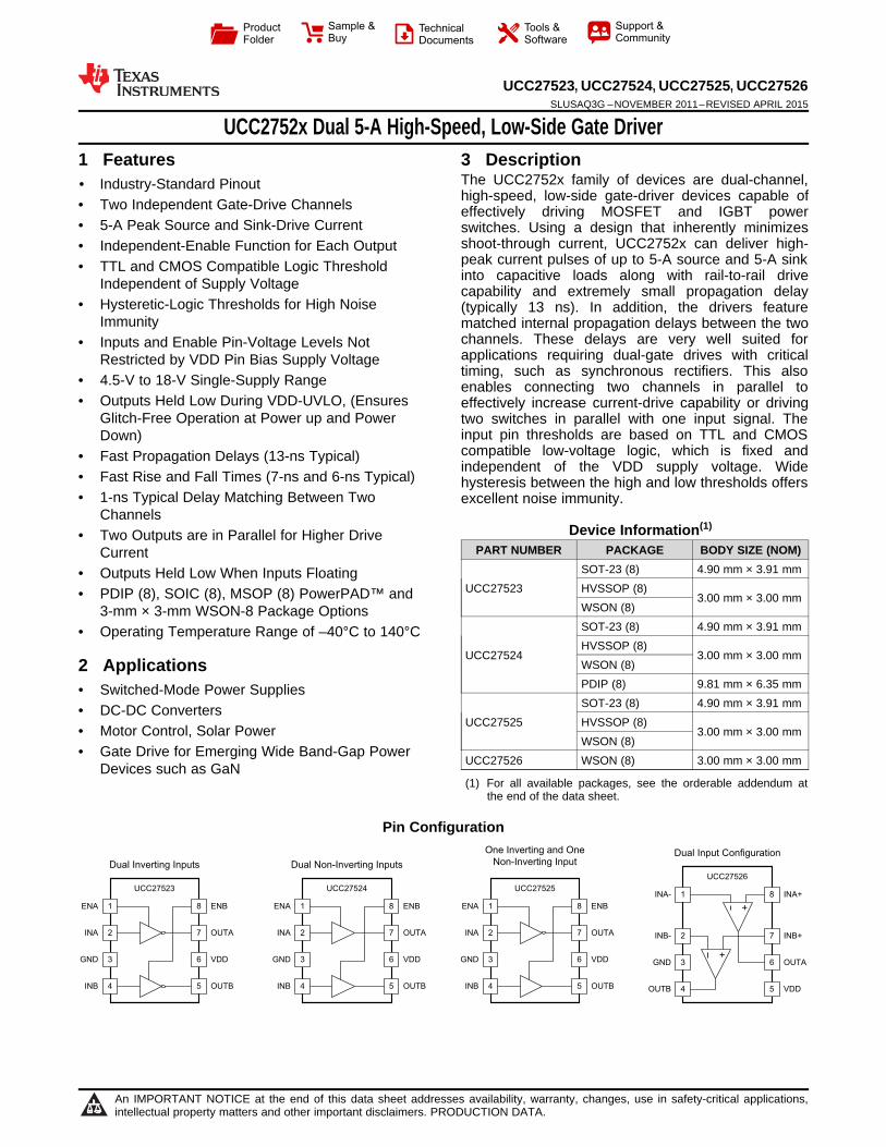
UCC27523
Dual Inverting Inputs
1
2
3
4
ENA
INA
GND
INB
8
7
6
5
ENB
OUTA
VDD
OUTB
UCC27524
Dual Non-Inverting Inputs
1
2
3
4
ENA
INA
GND
INB
8
7
6
5
ENB
OUTA
VDD
OUTB
UCC27525
One Inverting and One
Non-Inverting Input
1
2
3
4
INA-
INB-
GND
OUTB
8
7
6
5
INA+
INB+
OUTA
VDD
UCC27526
Dual Input Configuration
+
+
Product
Folder
Sample &Buy
Technical
Documents
Tools &
Software
Support &Community
UCC27523, UCC27524, UCC27525, UCC27526SLUSAQ3G –NOVEMBER 2011–REVISED APRIL 2015
UCC2752x Dual 5-A High-Speed, Low-Side Gate Driver1 Features 3 Description
The UCC2752x family of devices are dual-channel,1• Industry-Standard Pinout
high-speed, low-side gate-driver devices capable of• Two Independent Gate-Drive Channels effectively driving MOSFET and IGBT power• 5-A Peak Source and Sink-Drive Current switches. Using a design that inherently minimizes
shoot-through current, UCC2752x can deliver high-• Independent-Enable Function for Each Outputpeak current pulses of up to 5-A source and 5-A sink• TTL and CMOS Compatible Logic Threshold into capacitive loads along with rail-to-rail driveIndependent of Supply Voltage capability and extremely small propagation delay
• Hysteretic-Logic Thresholds for High Noise (typically 13 ns). In addition, the drivers featureImmunity matched internal propagation delays between the two
channels. These delays are very well suited for• Inputs and Enable Pin-Voltage Levels Notapplications requiring dual-gate drives with criticalRestricted by VDD Pin Bias Supply Voltagetiming, such as synchronous rectifiers. This also• 4.5-V to 18-V Single-Supply Range enables connecting two channels in parallel to
• Outputs Held Low During VDD-UVLO, (Ensures effectively increase current-drive capability or drivingGlitch-Free Operation at Power up and Power two switches in parallel with one input signal. The
input pin thresholds are based on TTL and CMOSDown)compatible low-voltage logic, which is fixed and• Fast Propagation Delays (13-ns Typical)independent of the VDD supply voltage. Wide
• Fast Rise and Fall Times (7-ns and 6-ns Typical) hysteresis between the high and low thresholds offers• 1-ns Typical Delay Matching Between Two excellent noise immunity.
ChannelsDevice Information(1)
• Two Outputs are in Parallel for Higher DrivePART NUMBER PACKAGE BODY SIZE (NOM)Current
SOT-23 (8) 4.90 mm × 3.91 mm• Outputs Held Low When Inputs FloatingUCC27523 HVSSOP (8)• PDIP (8), SOIC (8), MSOP (8) PowerPAD™ and 3.00 mm × 3.00 mm
WSON (8)3-mm × 3-mm WSON-8 Package OptionsSOT-23 (8) 4.90 mm × 3.91 mm• Operating Temperature Range of –40°C to 140°CHVSSOP (8)
UCC27524 3.00 mm × 3.00 mmWSON (8)2 ApplicationsPDIP (8) 9.81 mm × 6.35 mm• Switched-Mode Power SuppliesSOT-23 (8) 4.90 mm × 3.91 mm• DC-DC Converters
UCC27525 HVSSOP (8)• Motor Control, Solar Power 3.00 mm × 3.00 mmWSON (8)
• Gate Drive for Emerging Wide Band-Gap PowerUCC27526 WSON (8) 3.00 mm × 3.00 mmDevices such as GaN(1) For all available packages, see the orderable addendum at
the end of the data sheet.
Pin Configuration
1
An IMPORTANT NOTICE at the end of this data sheet addresses availability, warranty, changes, use in safety-critical applications,intellectual property matters and other important disclaimers. PRODUCTION DATA.

UCC27523, UCC27524, UCC27525, UCC27526SLUSAQ3G –NOVEMBER 2011–REVISED APRIL 2015 www.ti.com
Table of Contents8.3 Feature Description................................................. 131 Features .................................................................. 18.4 Device Functional Modes........................................ 202 Applications ........................................................... 1
9 Application and Implementation ........................ 213 Description ............................................................. 19.1 Application Information............................................ 214 Revision History..................................................... 29.2 Typical Application .................................................. 215 Description (continued)......................................... 4
10 Power Supply Recommendations ..................... 266 Pin Configuration and Functions ......................... 411 Layout................................................................... 267 Specifications......................................................... 6
11.1 Layout Guidelines ................................................. 267.1 Absolute Maximum Ratings ...................................... 611.2 Layout Example .................................................... 277.2 ESD Ratings.............................................................. 611.3 Thermal Considerations ........................................ 277.3 Recommended Operating Conditions....................... 6
12 Device and Documentation Support ................. 297.4 Thermal Information .................................................. 612.1 Related Links ........................................................ 297.5 Electrical Characteristics........................................... 712.2 Trademarks ........................................................... 297.6 Switching Characteristics .......................................... 812.3 Electrostatic Discharge Caution............................ 297.7 Typical Characteristics .............................................. 912.4 Glossary ................................................................ 298 Detailed Description ............................................ 12
13 Mechanical, Packaging, and Orderable8.1 Overview ................................................................. 12Information ........................................................... 298.2 Functional Block Diagrams ..................................... 12
4 Revision HistoryNOTE: Page numbers for previous revisions may differ from page numbers in the current version.
Changes from Revision F (May, 2013) to Revision G Page
• Added Pin Configuration and Functions section, ESD Ratings table, Feature Description section, Device FunctionalModes, Application and Implementation section, Power Supply Recommendations section, Layout section, Deviceand Documentation Support section, and Mechanical, Packaging, and Orderable Information section .............................. 1
• Changed UCC2752X Gate Driver Output Structure image. ................................................................................................. 17
Changes from Revision E (June 2012) to Revision F Page
• Added 0.5 to PSW equation in Drive Current and Power Dissipation section ....................................................................... 24
Changes from Revision D (April 2012) to Revision E Page
• Added OUTA, OUTB voltage field and values. ...................................................................................................................... 6• Changed table note from "Values are verified by characterization and are not production tested." to "Values are
verified by characterization on bench."................................................................................................................................... 6• Added note, "Values are verified by characterization and are not production tested." .......................................................... 6• Changed Switching Time tPW values from 10 ns and 25 ns to 15 ns and 25 ns ns. .............................................................. 7• Changed Functional Block Diagrams images....................................................................................................................... 12• Changed Slow Input Signal Figure 33.................................................................................................................................. 18
2 Submit Documentation Feedback Copyright © 2011–2015, Texas Instruments Incorporated
Product Folder Links: UCC27523 UCC27524 UCC27525 UCC27526

UCC27523, UCC27524, UCC27525, UCC27526www.ti.com SLUSAQ3G –NOVEMBER 2011–REVISED APRIL 2015
Changes from Revision C (March 2012) to Revision D Page
• Changed Inputs (INA, INB, INA+, INA–, INB+, INB-) section to include UCC2752X (D, DGN, DSD) information. ............... 7• Added Inputs (INA, INB, INA+, INA-, INB+, INB-) UCC27524P ONLY section. .................................................................... 7• Changed Enable (ENA, ENB) section to include UCC2752X (D, DGN, DSD) information.................................................... 7• Added ENABLE (ENA, ENB) UCC27524P ONLY section. .................................................................................................... 7
Changes from Revision B ( December 2011) to Revision C Page
• Added ROH note in the Outputs (OUTA, OUTB) section. ....................................................................................................... 7• Added an updated Output Stage section. ............................................................................................................................ 17• Added UCC2752X Gate Driver Output Structure image ...................................................................................................... 17• Added an updated Low Propagation Delays and Tightly Matched Outputs section. ........................................................... 18• Added Slow Input Signal Combined with Differences in Input Threshold Voltage image. ................................................... 18• Added updated Drive Current and Power Dissipation section. ............................................................................................ 23• Added a PSW... equation. .................................................................................................................................................... 24
Changes from Revision A (November 2011) to Revision B Page
• Changed Supply start threshold row to include two temperature ranges............................................................................... 7• Changed Minimum operating voltage after supply start min and max values from 3.6 V to 4.2 V to 3.40 V and 4.40 V. ..... 7• Changed Supply voltage hysteresis typ value from 0.35 to 0.30. .......................................................................................... 7• Changed UCC27526 Block Diagram drawing. ..................................................................................................................... 13• Changed UCC27526 Channel A in Inverting and Channel B in Non-Inverting Configuration drawing. ............................... 21
Changes from Original (November 2011) to Revision A Page
• Changed data sheet status to Production Data...................................................................................................................... 1
Copyright © 2011–2015, Texas Instruments Incorporated Submit Documentation Feedback 3
Product Folder Links: UCC27523 UCC27524 UCC27525 UCC27526

INA-
INB-
GND
OUTB
INA+
INB+
OUTA
VDD
1
2
3
4
8
7
6
5
INA-
INB-
GND
OUTB
INA+
INB+
OUTA
VDD
1
2
3
4
8
7
6
5
ENA
INA
GND
INB
ENB
OUTA
VDD
OUTB
1
2
3
4
8
7
6
5
ENA
INA
GND
INB
ENB
OUTA
VDD
OUTB
1
2
3
4
8
7
6
5
ENA
INA
GND
INB
ENB
OUTA
VDD
OUTB
1
2
3
4
8
7
6
5
ENA
INA
GND
INB
ENB
OUTA
VDD
OUTB
1
2
3
4
8
7
6
5
UCC27523, UCC27524, UCC27525, UCC27526SLUSAQ3G –NOVEMBER 2011–REVISED APRIL 2015 www.ti.com
5 Description (continued)The UCC2752x family provide the combination of three standard logic options — dual inverting, dualnoninverting, one inverting and one noninverting driver. UCC27526 features a dual input design which offersflexibility of both inverting (IN– pin) and non-inverting (IN+ pin) configuration for each channel. Either IN+ or IN–pin controls the state of the driver output. The unused input pin is used for enable and disable functions. Forsafety purpose, internal pullup and pulldown resistors on the input pins of all the devices in UCC2752x familyensure that outputs are held LOW when input pins are in floating condition. The UCC27523, UCC27524, andUCC27525 devices feature Enable pins (ENA and ENB) to have better control of the operation of the driverapplications. The pins are internally pulled up to VDD for active-high logic and are left open for standardoperation.
UCC2752x family of devices are available in SOIC-8 (D), MSOP-8 with exposed pad (DGN) and 3-mm × 3-mmWSON-8 with exposed pad (DSD) packages. UCC27524 is also offered in PDIP-8 (P) package. UCC27526 isonly offered in 3-mm × 3-mm WSON (DSD) package.
6 Pin Configuration and Functions
D, DGN, or P Package UCC2752(3,4,5)DSD Package UCC2752(3,4,5)8-Pin SOT-23, HVSSOP, or PDIP
8-Pin WSONTop ViewTop View
DSD Package UCC275268-Pin WSON
Top View
4 Submit Documentation Feedback Copyright © 2011–2015, Texas Instruments Incorporated
Product Folder Links: UCC27523 UCC27524 UCC27525 UCC27526

UCC27523, UCC27524, UCC27525, UCC27526www.ti.com SLUSAQ3G –NOVEMBER 2011–REVISED APRIL 2015
Pin Functions (UCC27523 / UCC27524 / UCC27525)PIN
I/O DESCRIPTIONNO. NAME
Enable input for Channel A: ENA biased LOW Disables Channel A output regardless of INA state,1 ENA I ENA biased HIGH or floating Enables Channel A output, ENA allowed to float hence the pin-to-pin
compatibility with UCC2732X N/C pin.Input to Channel A: Inverting Input in UCC27523, Non-Inverting Input in UCC27524, Inverting2 INA I Input in UCC27525, OUTA held LOW if INA is unbiased or floating.
3 GND - Ground: All signals referenced to this pin.Input to Channel B: Inverting Input in UCC27523, Non-Inverting Input in UCC27524, Non-Inverting4 INB I Input in UCC27525, OUTB held LOW if INB is unbiased or floating.
5 OUTB O Output of Channel B6 VDD I Bias supply input7 OUTA O Output of Channel A
Enable input for Channel B: ENB biased LOW Disables Channel B output regardless of INB state,8 ENB I ENB biased HIGH or floating Enables Channel B output, ENB allowed to float hence the pin-to-pin
compatibility with UCC2732X N/C pin.
Pin Functions (UCC27526)PIN
I/O DESCRIPTIONNO. NAME
Inverting Input to Channel A: When Channel A is used in Non-Inverting configuration, connect1 INA– I INA– to GND in order to Enable Channel A output, OUTA held LOW if INA– is unbiased or floating.Inverting Input to Channel B: When Channel B is used in Non-Inverting configuration, connect2 INB– I INB– to GND in order to Enable Channel B output, OUTB held LOW if INB– is unbiased or floating.
3 GND - Ground: All signals referenced to this pin.4 OUTB I Output of Channel B5 VDD O Bias Supply Input6 OUTA I Output of Channel A
Non-Inverting Input to Channel B: When Channel B is used in Inverting configuration, connect7 INB+ O INB+ to VDD in order to Enable Channel B output, OUTB held LOW if INB+ is unbiased or floating.Non-Inverting Input to Channel A: When Channel A is used in Inverting configuration, connect8 INA+ I INA+ to VDD in order to Enable Channel A output, OUTA held LOW if INA+ is unbiased or floating.
Copyright © 2011–2015, Texas Instruments Incorporated Submit Documentation Feedback 5
Product Folder Links: UCC27523 UCC27524 UCC27525 UCC27526

UCC27523, UCC27524, UCC27525, UCC27526SLUSAQ3G –NOVEMBER 2011–REVISED APRIL 2015 www.ti.com
7 Specifications
7.1 Absolute Maximum Ratings (1) (2)
over operating free-air temperature range (unless otherwise noted)MIN MAX UNIT
Supply voltage VDD –0.3 20DC –0.3 VDD + 0.3 V
OUTA, OUTB voltageRepetitive pulse < 200 ns (3) –2 VDD + 0.3
Output continuous source/sink IOUT_DC 0.3currentA
Output pulsed source/sink current IOUT_pulsed 5(0.5 µs)INA, INB, INA+, INA–, INB+, INB–, ENA, ENB voltage (4) –0.3 20 VOperating virtual junction temperature, TJ –40 150
Soldering, 10 s 300 °CLead temperature
Reflow 260Storage temperature, Tstg –65 150 °C
(1) Stresses beyond those listed under Absolute Maximum Ratings may cause permanent damage to the device. These are stress ratingsonly and functional operation of the device at these or any other conditions beyond those indicated under Recommended OperatingConditions is not implied. Exposure to absolute-maximum-rated conditions for extended periods may affect device reliability.
(2) All voltages are with respect to GND unless otherwise noted. Currents are positive into, negative out of the specified terminal. SeeMechanical, Packaging, and Orderable Information for thermal limitations and considerations of packages.
(3) Values are verified by characterization on bench.(4) The maximum voltage on the Input and Enable pins is not restricted by the voltage on the VDD pin.
7.2 ESD RatingsVALUE UNIT
Human body model (HBM), per ANSI/ESDA/JEDEC JS-001 (1) ±4000V(ESD) Electrostatic discharge VCharged-device model (CDM), per JEDEC specification JESD22- ±1000
C101 (2)
(1) JEDEC document JEP155 states that 500-V HBM allows safe manufacturing with a standard ESD control process.(2) JEDEC document JEP157 states that 250-V CDM allows safe manufacturing with a standard ESD control process.
7.3 Recommended Operating Conditionsover operating free-air temperature range (unless otherwise noted)
MIN NOM MAX UNITSupply voltage, VDD 4.5 12 18 VOperating junction temperature –40 140 °CInput voltage, INA, INB, INA+, INA–, INB+, INB– 0 18 VEnable voltage, ENA and ENB 0 18
7.4 Thermal InformationUCC27523/4/5 UCC27524 UCC27523/4/5/6
THERMAL METRIC (1) SOIC (D) MSOP (DGN) PDIP (P) WSON (DSD) UNIT8 PINS 8 PINS 8 PINS 8 PINS
RθJA Junction-to-ambient thermal resistance 130.9 71.8 62.1 46.7RθJC(top) Junction-to-case (top) thermal resistance 80 65.6 52.7 46.7RθJB Junction-to-board thermal resistance 71.4 7.4 39.1 22.4
°C/WψJT Junction-to-top characterization parameter 21.9 7.4 31 0.7ψJB Junction-to-board characterization parameter 70.9 31.5 39.1 22.6RθJC(bot) Junction-to-case (bottom) thermal resistance – 19.6 – 9.5
(1) For more information about traditional and new thermal metrics, see the IC Package Thermal Metrics application report, SPRA953.
6 Submit Documentation Feedback Copyright © 2011–2015, Texas Instruments Incorporated
Product Folder Links: UCC27523 UCC27524 UCC27525 UCC27526
UCC27523, UCC27524, UCC27525, UCC27526www.ti.com SLUSAQ3G –NOVEMBER 2011–REVISED APRIL 2015
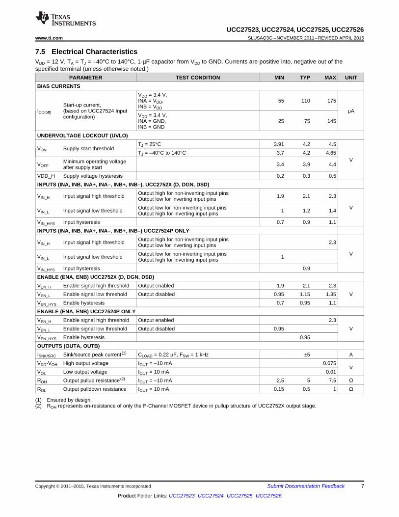
7.5 Electrical CharacteristicsVDD = 12 V, TA = TJ = –40°C to 140°C, 1-µF capacitor from VDD to GND. Currents are positive into, negative out of thespecified terminal (unless otherwise noted,)
PARAMETER TEST CONDITION MIN TYP MAX UNITBIAS CURRENTS
VDD = 3.4 V,INA = VDD, 55 110 175
Start-up current, INB = VDDIDD(off) (based on UCC27524 Input μAVDD = 3.4 V,configuration)INA = GND, 25 75 145INB = GND
UNDERVOLTAGE LOCKOUT (UVLO)TJ = 25°C 3.91 4.2 4.5
VON Supply start thresholdTJ = –40°C to 140°C 3.7 4.2 4.65
VMinimum operating voltageVOFF 3.4 3.9 4.4after supply startVDD_H Supply voltage hysteresis 0.2 0.3 0.5INPUTS (INA, INB, INA+, INA–, INB+, INB–), UCC2752X (D, DGN, DSD)
Output high for non-inverting input pinsVIN_H Input signal high threshold 1.9 2.1 2.3Output low for inverting input pinsOutput low for non-inverting input pins VVIN_L Input signal low threshold 1 1.2 1.4Output high for inverting input pins
VIN_HYS Input hysteresis 0.7 0.9 1.1INPUTS (INA, INB, INA+, INA–, INB+, INB–) UCC27524P ONLY
Output high for non-inverting input pinsVIN_H Input signal high threshold 2.3Output low for inverting input pinsOutput low for non-inverting input pins VVIN_L Input signal low threshold 1Output high for inverting input pins
VIN_HYS Input hysteresis 0.9ENABLE (ENA, ENB) UCC2752X (D, DGN, DSD)VEN_H Enable signal high threshold Output enabled 1.9 2.1 2.3VEN_L Enable signal low threshold Output disabled 0.95 1.15 1.35 VVEN_HYS Enable hysteresis 0.7 0.95 1.1ENABLE (ENA, ENB) UCC27524P ONLYVEN_H Enable signal high threshold Output enabled 2.3VEN_L Enable signal low threshold Output disabled 0.95 VVEN_HYS Enable hysteresis 0.95OUTPUTS (OUTA, OUTB)ISNK/SRC Sink/source peak current (1) CLOAD = 0.22 µF, FSW = 1 kHz ±5 AVDD-VOH High output voltage IOUT = –10 mA 0.075
VVOL Low output voltage IOUT = 10 mA 0.01ROH Output pullup resistance (2) IOUT = –10 mA 2.5 5 7.5 ΩROL Output pulldown resistance IOUT = 10 mA 0.15 0.5 1 Ω
(1) Ensured by design.(2) ROH represents on-resistance of only the P-Channel MOSFET device in pullup structure of UCC2752X output stage.
Copyright © 2011–2015, Texas Instruments Incorporated Submit Documentation Feedback 7
Product Folder Links: UCC27523 UCC27524 UCC27525 UCC27526

10%
90%
Enable
Output
Low
High
Low
High
Input
tD1 tD2UDG-11219
10%
90%
Enable
Output
Low
High
Low
High
Input
tD1 tD2UDG-11220
10%
90%
Enable
Output
Low
High
Low
High
Input
tD3 tD4 UDG-11217
10%
90%
Enable
Output
Low
High
Low
High
Input
tD3 tD4 UDG-11218
UCC27523, UCC27524, UCC27525, UCC27526SLUSAQ3G –NOVEMBER 2011–REVISED APRIL 2015 www.ti.com
7.6 Switching Characteristicsover operating free-air temperature range (unless otherwise noted)
PARAMETER TEST CONDITIONS MIN TYP MAX UNITtR Rise time (1) CLOAD = 1.8 nF 7 18tF Fall time (1) CLOAD = 1.8 nF 6 10
INA = INB, OUTA and OUTB at 50%tM Delay matching between 2 channels 1 4transition pointns
Minimum input pulse width thattPW 15 25changes the output statetD1, tD2 Input to output propagation delay (1) CLOAD = 1.8 nF, 5-V input pulse 6 13 23tD3, tD4 EN to output propagation delay (1) CLOAD = 1.8 nF, 5-V enable pulse 6 13 23
(1) See timing diagrams in Figure 1, Figure 2, Figure 3, and Figure 4
Figure 1. Enable Function Figure 2. Enable Function(For Non-Inverting Input Driver Operation) (For Inverting Input Driver Operation)
Figure 3. Non-Inverting Input Driver Operation Figure 4. Inverting Input Driver Operation
8 Submit Documentation Feedback Copyright © 2011–2015, Texas Instruments Incorporated
Product Folder Links: UCC27523 UCC27524 UCC27525 UCC27526

0.5
1
1.5
2
2.5
−50 0 50 100 150Temperature (°C)
Inpu
t Thr
esho
ld (
V)
Input High ThresholdInput Low Threshold
VDD = 12 V
G004
0.5
1
1.5
2
2.5
−50 0 50 100 150Temperature (°C)
Ena
ble
Thr
esho
ld (
V)
Enable High ThresholdEnable Low Threshold
VDD = 12 V
G005
0.2
0.3
0.4
0.5
0.6
−50 0 50 100 150Temperature (°C)
Sup
ply
Cur
rent
(m
A)
Input=GNDInput=VDD
Enable=12 VVDD = 12 V
G012
3
3.5
4
4.5
5
−50 0 50 100 150Temperature (°C)
UV
LO T
hres
hold
(V
)
UVLO RisingUVLO Falling
G003
0.06
0.08
0.1
0.12
0.14
−50 0 50 100 150Temperature (°C)
Sta
rtup
Cur
rent
(m
A)
Input=VDD Input=GND
VDD=3.4V
G001
2.5
3
3.5
4
−50 0 50 100 150Temperature (°C)
Ope
ratin
g S
uppl
y C
urre
nt (
mA
)
VDD = 12 VfSW = 500 kHzCL = 500 pF
G002
UCC27523, UCC27524, UCC27525, UCC27526www.ti.com SLUSAQ3G –NOVEMBER 2011–REVISED APRIL 2015
7.7 Typical Characteristics
Figure 5. Start-Up Current vs Temperature Figure 6. Operating Supply Current vs Temperature(Outputs Switching)
Figure 7. Supply Current vs Temperature (Outputs in DC Figure 8. UVLO Threshold vs TemperatureON/OFF Condition)
Figure 9. Input Threshold vs Temperature Figure 10. Enable Threshold vs Temperature
Copyright © 2011–2015, Texas Instruments Incorporated Submit Documentation Feedback 9
Product Folder Links: UCC27523 UCC27524 UCC27525 UCC27526

8
10
12
14
16
18
−50 0 50 100 150Temperature (°C)
Inpu
t to
Out
put P
ropa
gatio
n D
elay
(ns
)
Turn−onTurn−off
VDD = 12 VCLOAD = 1.8 nF
G010
8
10
12
14
16
18
−50 0 50 100 150Temperature (°C)
EN
to O
utpu
t Pro
paga
tion
Del
ay (
ns) EN to Output High
EN to Output Low
VDD = 12 VCLOAD = 1.8 nF
G011
5
6
7
8
9
10
−50 0 50 100 150Temperature (°C)
Ris
e T
ime
(ns)
VDD = 12 VCLOAD = 1.8 nF
G008
5
6
7
8
9
−50 0 50 100 150Temperature (°C)
Fal
l Tim
e (n
s)
VDD = 12 VCLOAD = 1.8 nF
G009
3
4
5
6
7
−50 0 50 100 150Temperature (°C)
Out
put P
ull−
up R
esis
tanc
e (Ω
)
VDD = 12 VIOUT = −10 mA
G006
0.2
0.4
0.6
0.8
1
−50 0 50 100 150Temperature (°C)
Out
put P
ull−
dow
n R
esis
tanc
e (Ω
) VDD = 12 VIOUT = 10 mA
G007
UCC27523, UCC27524, UCC27525, UCC27526SLUSAQ3G –NOVEMBER 2011–REVISED APRIL 2015 www.ti.com
Typical Characteristics (continued)
Figure 11. Output Pullup Resistance vs Temperature Figure 12. Output Pulldown Resistance vs Temperature
Figure 13. Rise Time vs Temperature Figure 14. Fall Time vs Temperature
Figure 15. Input to Output Propagation Delay vs Figure 16. EN to Output Propagation Delay vs TemperatureTemperature
10 Submit Documentation Feedback Copyright © 2011–2015, Texas Instruments Incorporated
Product Folder Links: UCC27523 UCC27524 UCC27525 UCC27526

0.5
1
1.5
2
2.5
−50 0 50 100 150Temperature (°C)
Ena
ble
Thr
esho
ld (
V)
Enable High ThresholdEnable Low Threshold
VDD = 4.5 V
G017
6
10
14
18
4 8 12 16 20Supply Voltage (V)
Ris
e T
ime
(ns)
CLOAD = 1.8 nF
G015
4
6
8
10
4 8 12 16 20Supply Voltage (V)
Fal
l Tim
e (n
s)
CLOAD = 1.8 nF
G016
0
10
20
30
40
50
60
0 100 200 300 400 500 600 700 800 900 1000Frequency (kHz)
Ope
ratin
g S
uppl
y C
urre
nt (
mA
)
VDD = 4.5 VVDD = 12 VVDD = 15 V
CLOAD = 1.8 nFBoth channels switching
G013
6
10
14
18
22
4 8 12 16 20Supply Voltage (V)
Pro
paga
tion
Del
ays
(ns)
Input to Output On delayInput to Ouptut Off DelayEN to Output On DelayEN to Output Off Delay
CLOAD = 1.8 nF
G014
UCC27523, UCC27524, UCC27525, UCC27526www.ti.com SLUSAQ3G –NOVEMBER 2011–REVISED APRIL 2015
Typical Characteristics (continued)
Figure 17. Operating Supply Current vs Frequency Figure 18. Propagation Delays vs Supply Voltage
Figure 19. Rise Time vs Supply Voltage Figure 20. Fall Time vs Supply Voltage
Figure 21. Enable Threshold vs Temperature
Copyright © 2011–2015, Texas Instruments Incorporated Submit Documentation Feedback 11
Product Folder Links: UCC27523 UCC27524 UCC27525 UCC27526

1ENA
200 kW
VDD
2
INA
400 kW
3GND
4INB
400 kW
UVLO
VDD
VDD
VDD
8
7
6
5
ENB
OUTA
VDD
OUTB
200 kW
VDD
VDD
1ENA
200 kW
VDD
2INA
200 kW
VDD
3GND
4INB
200 kW
VDD UVLO
VDD
VDD
VDD
8
7
6
5
ENB
OUTA
VDD
OUTB
200 kW
VDD
VDD
UDG-11221
UCC27523, UCC27524, UCC27525, UCC27526SLUSAQ3G –NOVEMBER 2011–REVISED APRIL 2015 www.ti.com
8 Detailed Description
8.1 OverviewThe UCC2752x family of products represent TI’s latest generation of dual-channel, low-side, high-speed gate-driver devices featuring 5-A source and sink current capability, industry best-in-class switching characteristicsand a host of other features listed in Table 1 all of which combine to ensure efficient, robust and reliableoperation in high-frequency switching power circuits.
Table 1. UCC2752x Family of Features and BenefitsFEATURE BENEFIT
Best-in-class 13-ns (typ) propagation delay Extremely low-pulse transmission distortion1-ns (typ) delay matching between channels Ease of paralleling outputs for higher (2 times) current capability,
ease of driving parallel-power switchesExpanded VDD Operating range of 4.5 to 18 V Flexibility in system designExpanded operating temperature range of –40°C to 140°C(See Electrical Characteristics)VDD UVLO Protection Outputs are held Low in UVLO condition, which ensures predictable,
glitch-free operation at power-up and power-downOutputs held Low when input pins (INx) in floating condition Safety feature, especially useful in passing abnormal condition tests
during safety certificationOutputs enable when enable pins (ENx) in floating condition Pin-to-pin compatibility with UCC2732X family of products from TI, in
designs where pin 1 and 8 are in floating conditionCMOS/TTL compatible input and enable threshold with wide Enhanced noise immunity, while retaining compatibility withhysteresis microcontroller logic level input signals (3.3 V, 5 V) optimized for
digital powerAbility of input and enable pins to handle voltage levels not restricted System simplification, especially related to auxiliary bias supplyby VDD pin bias voltage architecture
8.2 Functional Block Diagrams
Figure 22. UCC27523 Block Diagram Figure 23. UCC27524 Block Diagram
12 Submit Documentation Feedback Copyright © 2011–2015, Texas Instruments Incorporated
Product Folder Links: UCC27523 UCC27524 UCC27525 UCC27526

8INA+
200 kW
VDD
1INA-
400 kW
3GND
7INB+
400 kW
UVLO
VDD
VDD
VDD
6
5
4
OUTA
VDD
OUTB
VDD
UDG-11222
2INB-200 kW
VDD
1ENA
200 kW
VDD
2INA
3GND
4INB
400 kW
UVLO
VDD
VDD
VDD
8
7
6
5
ENB
OUTA
VDD
OUTB
200 kW
VDD
VDD
UDG-11223
200 kW
VDD
UCC27523, UCC27524, UCC27525, UCC27526www.ti.com SLUSAQ3G –NOVEMBER 2011–REVISED APRIL 2015
Functional Block Diagrams (continued)
Figure 24. UCC27525 Block Diagram Figure 25. UCC27526 Block Diagram
8.3 Feature Description
8.3.1 VDD and Undervoltage LockoutThe UCC2752x devices have internal undervoltage-lockout (UVLO) protection feature on the VDD pin supplycircuit blocks. When VDD is rising and the level is still below UVLO threshold, this circuit holds the output LOW,regardless of the status of the inputs. The UVLO is typically 4.2 V with 300-mV typical hysteresis. This hysteresisprevents chatter when low VDD supply voltages have noise from the power supply and also when there aredroops in the VDD bias voltage when the system commences switching and there is a sudden increase in IDD.The capability to operate at low voltage levels such as below 5 V, along with best-in-class switchingcharacteristics, is especially suited for driving emerging GaN power semiconductor devices.
For example, at power up, the UCC2752x driver-device output remains LOW until the VDD voltage reaches theUVLO threshold if Enable pin is active or floating. The magnitude of the OUT signal rises with VDD until steady-state VDD is reached. The non-inverting operation in Figure 26 shows that the output remains LOW until theUVLO threshold is reached, and then the output is in-phase with the input. The inverting operation in Figure 27shows that the output remains LOW until the UVLO threshold is reached, and then the output is out-phase withthe input. With UCC27526 the output turns to high-state only if INX+ is high and INX– is low after the UVLOthreshold is reached.
Because the device draws current from the VDD pin to bias all internal circuits, for the best high-speed circuitperformance, TI recommends two VDD bypass capacitors to prevent noise problems. TI highly recommends usingsurface-mount components. A 0.1-μF ceramic capacitor must be located as close as possible to the VDD to GNDpins of the gate-driver device. In addition, a larger capacitor (such as 1-μF) with relatively low ESR must beconnected in parallel and close proximity, in order to help deliver the high-current peaks required by the load.The parallel combination of capacitors presents a low impedance characteristic for the expected current levelsand switching frequencies in the application.
Copyright © 2011–2015, Texas Instruments Incorporated Submit Documentation Feedback 13
Product Folder Links: UCC27523 UCC27524 UCC27525 UCC27526

VDD
EN
IN
OUT
VDD Threshold
UDG-11228
VDD
EN
IN
OUT
VDD Threshold
UDG-11229
UCC27523, UCC27524, UCC27525, UCC27526SLUSAQ3G –NOVEMBER 2011–REVISED APRIL 2015 www.ti.com
Feature Description (continued)
Figure 27. Power up Inverting DriverFigure 26. Power up Non-Inverting Driver
8.3.2 Operating Supply CurrentThe UCC2752x products feature very low quiescent IDD currents. The typical operating-supply current in UVLOstate and fully on state (under static and switching conditions) are summarized in Figure 5, Figure 6 andFigure 7. The IDD current when the device is fully on and outputs are in a static state (DC high or DC low, referFigure 6) represents lowest quiescent IDD current when all the internal logic circuits of the device are fullyoperational. The total supply current is the sum of the quiescent IDD current, the average IOUT current due toswitching and finally any current related to pullup resistors on the enable pins and inverting input pins. Forexample when the inverting Input pins are pulled low additional current is drawn from VDD supply through thepullup resistors (refer to Figure 22 though Figure 25). Knowing the operating frequency (fSW) and the MOSFETgate (QG) charge at the drive voltage being used, the average IOUT current can be calculated as product of QGand fSW.
A complete characterization of the IDD current as a function of switching frequency at different VDD bias voltagesunder 1.8-nF switching load in both channels is provided in Figure 17. The strikingly linear variation and closecorrelation with theoretical value of average IOUT indicates negligible shoot-through inside the gate-driver deviceattesting to its high-speed characteristics.
14 Submit Documentation Feedback Copyright © 2011–2015, Texas Instruments Incorporated
Product Folder Links: UCC27523 UCC27524 UCC27525 UCC27526
UCC27523, UCC27524, UCC27525, UCC27526www.ti.com SLUSAQ3G –NOVEMBER 2011–REVISED APRIL 2015
Feature Description (continued)8.3.3 Input StageThe input pins of UCC2752x gate-driver devices are based on a TTL and CMOS compatible input-threshold logicthat is independent of the VDD supply voltage. With typically high threshold = 2.1 V and typically low threshold =1.2 V, the logic level thresholds are conveniently driven with PWM control signals derived from 3.3-V and 5-Vdigital power-controller devices. Wider hysteresis (typ 0.9 V) offers enhanced noise immunity compared totraditional TTL logic implementations, where the hysteresis is typically less than 0.5 V. UCC2752x devices alsofeature tight control of the input pin threshold voltage levels which eases system design considerations andensures stable operation across temperature (refer to Figure 9). The very low input capacitance on these pinsreduces loading and increases switching speed.
The UCC2752x devices feature an important safety feature wherein, whenever any of the input pins is in afloating condition, the output of the respective channel is held in the low state. This is achieved using VDD pullupresistors on all the Inverting inputs (INA, INB in UCC27523, INA in UCC27525 and INA–, INB– in UCC27526) orGND pulldown resistors on all the non-inverting input pins (INA, INB in UCC27524, INB in UCC27525 and INA+,INB+ in UCC27526), as shown in the device block diagrams.
While UCC27523/4/5 devices feature one input pin per channel, the UCC27526 features a dual inputconfiguration with two input pins available to control the output state of each channel. With the UCC27526 devicethe user has the flexibility to drive each channel using either a non-inverting input pin (INx+) or an inverting inputpin (INx–). The state of the output pin is dependent on the bias on both the INx+ and INx– pins (where x = A, B).Once an Input pin is chosen to drive a channel, the other input pin of that channel (the unused input pin) must beproperly biased in order to enable the output of the channel. The unused input pin cannot remain in a floatingcondition because, as mentioned earlier, whenever any input pin is left in a floating condition, the output of thatchannel is disabled using the internal pullup or pulldown resistors for safety purposes. Alternatively, the unusedinput pin is used effectively to implement an enable/disable function, as explained below.• In order to drive the channel x (x = A or B) in a non-inverting configuration, apply the PWM control input
signal to INx+ pin. In this case, the unused input pin, INx-, must be biased low (for example, tied to GND) inorder to enable the output of this channel.– Alternately, the INx– pin can be used to implement the enable/disable function using an external logic
signal. OUTx is disabled when INx- is biased High and OUTx is enabled when INX– is biased low.• In order to drive the channel x (x = A or B) in an Inverting configuration, apply the PWM control input signal to
INX– pin. In this case, the unused input pin, INX+, must be biased high (for example, tied to VDD) in order toenable the output of the channel.– Alternately, the INX+ pin can be used to implement the enable/disable function using an external logic
signal. OUTX is disabled when INX+ is biased low and OUTX is enabled when INX+ is biased high.• Finally, it is worth noting that the UCC27526 output pin can be driven into high state only when INx+ pin is
biased high and INx- input is biased low.
Refer to the input/output logic truth table and typical application diagrams, (Figure 34, Figure 35, and Figure 35),for additional clarification.
The input stage of each driver is driven by a signal with a short rise or fall time. This condition is satisfied intypical power supply applications, where the input signals are provided by a PWM controller or logic gates withfast transition times (< 200 ns) with a slow changing input voltage, the output of the driver may switch repeatedlyat a high frequency. While the wide hysteresis offered in UCC2752x definitely alleviates this concern over mostother TTL input threshold devices, extra care is necessary in these implementations. If limiting the rise or falltimes to the power device is the primary goal, then TI highly recommends an external resistance between theoutput of the driver and the power device. This external resistor has the additional benefit of reducing part of thegate-charge related power dissipation in the gate-driver device package and transferring it into the externalresistor itself.
Copyright © 2011–2015, Texas Instruments Incorporated Submit Documentation Feedback 15
Product Folder Links: UCC27523 UCC27524 UCC27525 UCC27526

UCC27523, UCC27524, UCC27525, UCC27526SLUSAQ3G –NOVEMBER 2011–REVISED APRIL 2015 www.ti.com
Feature Description (continued)8.3.4 Enable FunctionThe enable function is an extremely beneficial feature in gate-driver devices especially for certain applicationssuch as synchronous rectification where the driver outputs disable in light-load conditions to prevent negativecurrent circulation and to improve light-load efficiency.
UCC27523/4/5 devices are provided with independent enable pins ENx for exclusive control of each driver-channel operation. The enable pins are based on a non-inverting configuration (active-high operation). Thuswhen ENx pins are driven high the drivers are enabled and when ENx pins are driven low the drivers aredisabled. Like the input pins, the enable pins are also based on a TTL and CMOS compatible input-thresholdlogic that is independent of the supply voltage and are effectively controlled using logic signals from 3.3-V and 5-V microcontrollers. The UCC2752X devices also feature tight control of the Enable-function threshold-voltagelevels which eases system design considerations and ensures stable operation across temperature (refer toFigure 10). The ENx pins are internally pulled up to VDD using pullup resistors as a result of which the outputs ofthe device are enabled in the default state. Hence the ENx pins are left floating or Not Connected (N/C) forstandard operation, where the enable feature is not needed. Essentially, this floating allows the UCC27523/4/5devices to be pin-to-pin compatible with TI’s previous generation drivers UCC27323/4/5 respectively, where pins1, 8 are N/C pins. If the Channel A and Channel B inputs and outputs are connected in parallel to increase thedriver current capacity, ENA and ENB are connected and driven together.
The UCC27526 device does not feature dedicated enable pins. However, as mentioned earlier, anenable/disable function is easily implemented in UCC27526 using the unused input pin. When INx+ is pulleddown to GND or INx– is pulled down to VDD, the output is disabled. Thus INx+ pin is used like an enable pin thatis based on active high logic, while INx– is used like an enable pin that is based on active low logic. Note thatwhile the ENA, ENB pins in UCC27523/4/5 are allowed to be in floating condition during standard operation andthe outputs will be enabled, the INx+, INx– pins in UCC27526 are not allowed to be floating because this willdisable the outputs.
16 Submit Documentation Feedback Copyright © 2011–2015, Texas Instruments Incorporated
Product Folder Links: UCC27523 UCC27524 UCC27525 UCC27526

VCC
ROH
ROL
Gate
Voltage
Boost
Narrow Pulse at
each Turn On
Anti Shoot-
Through
Circuitry
Input Signal
RNMOS, Pull Up
OUT
UCC27523, UCC27524, UCC27525, UCC27526www.ti.com SLUSAQ3G –NOVEMBER 2011–REVISED APRIL 2015
Feature Description (continued)8.3.5 Output StageThe UCC2752x device output stage features a unique architecture on the pullup structure which delivers thehighest peak-source current when it is most needed during the Miller plateau region of the power-switch turnontransition (when the power switch drain or collector voltage experiences dV/dt). The output stage pullup structurefeatures a P-channel MOSFET and an additional N-channel MOSFET in parallel. The function of the N-channelMOSFET is to provide a brief boost in the peak sourcing current enabling fast turnon. This is accomplished bybriefly turning-on the N-channel MOSFET during a narrow instant when the output is changing state from Low toHigh.
Figure 28. UCC2752x Gate Driver Output Structure
The ROH parameter (see Electrical Characteristics) is a DC measurement and it is representative of the on-resistance of the P-Channel device only. This is because the N-Channel device is held in the off state in DCcondition and is turned-on only for a narrow instant when output changes state from low to high. Note thateffective resistance of UCC2752x pullup stage during the turnon instant is much lower than what is representedby ROH parameter.
The pulldown structure in UCC2752x is simply composed of a N-Channel MOSFET. The ROL parameter (seeElectrical Characteristics), which is also a DC measurement, is representative of the impedance of the pulldownstage in the device. In UCC2752x, the effective resistance of the hybrid pullup structure during turnon isestimated to be approximately 1.5 × ROL, estimated based on design considerations.
Each output stage in UCC2752x can supply 5-A peak source and 5-A peak sink current pulses. The outputvoltage swings between VDD and GND providing rail-to-rail operation, thanks to the MOS-output stage whichdelivers very low drop-out. The presence of the MOSFET-body diodes also offers low impedance to switchingovershoots and undershoots which means that in many cases, external Schottky-diode clamps may beeliminated. The outputs of these drivers are designed to withstand 500-mA reverse current without eitherdamage to the device or logic malfunction.
The UCC2752x devices are particularly suited for dual-polarity, symmetrical drive-gate transformer applicationswhere the primary winding of transformer driven by OUTA and OUTB, with inputs INA and INB being drivencomplementary to each other. This situation is due to the extremely low drop-out offered by the MOS outputstage of these devices, both during high (VOH) and low (VOL) states along with the low impedance of the driveroutput stage, all of which allow alleviate concerns regarding transformer demagnetization and flux imbalance.The low propagation delays also ensure accurate reset for high-frequency applications.
Copyright © 2011–2015, Texas Instruments Incorporated Submit Documentation Feedback 17
Product Folder Links: UCC27523 UCC27524 UCC27525 UCC27526

1ENA
200 kW
VDD
2INA
400 kW
3GND
4INB
400 kW
UVLO
VDD
VDD
VDD
8
7
6
5
ENB
OUTA
VDD
OUTB
200 kW
VDD
VDD
ISHOOT-THROUGH
VIN_H
(Channel B)
VIN_H
(Channel A)
Slow Input Signal
UCC27523, UCC27524, UCC27525, UCC27526SLUSAQ3G –NOVEMBER 2011–REVISED APRIL 2015 www.ti.com
Feature Description (continued)For applications that have zero voltage switching during power MOSFET turnon or turnoff interval, the driversupplies high-peak current for fast switching even though the miller plateau is not present. This situation oftenoccurs in synchronous rectifier applications because the body diode is generally conducting before powerMOSFET is switched on.
8.3.6 Low Propagation Delays and Tightly Matched OutputsThe UCC2752x driver devices feature a best in class, 13-ns (typical) propagation delay between input and outputwhich goes to offer the lowest level of pulse-transmission distortion available in the industry for high frequencyswitching applications. For example in synchronous rectifier applications, the SR MOSFETs are driven with verylow distortion when one driver device is used to drive both the SR MOSFETs. Further, the driver devices alsofeature an extremely accurate, 1-ns (typ) matched internal-propagation delays between the two channels whichis beneficial for applications requiring dual gate drives with critical timing. For example in a PFC application, apair of paralleled MOSFETs may be driven independently using each output channel, which the inputs of bothchannels are driven by a common control signal from the PFC controller device. In this case the 1ns delaymatching ensures that the paralleled MOSFETs are driven in a simultaneous fashion with the minimum of turnondelay difference. Yet another benefit of the tight matching between the two channels is that the two channels areconnected together to effectively increase current drive capability, for example A and B channels may becombined into one driver by connecting the INA and INB inputs together and the OUTA and OUTB outputstogether. Then, one signal controls the paralleled combination.
Caution must be exercised when directly connecting OUTA and OUTB pins together because there is thepossibility that any delay between the two channels during turnon or turnoff may result in shoot-through currentconduction as shown in Figure 29. While the two channels are inherently very well matched (4-ns Maxpropagation delay), note that there may be differences in the input threshold voltage level between the twochannels which causes the delay between the two outputs especially when slow dV/dt input signals areemployed. TI recommends the following guidelines whenever the two driver channels are paralleled using directconnections between OUTA and OUTB along with INA and INB:• Use very fast dV/dt input signals (20 V/µs or greater) on INA and INB pins to minimize impact of differences
in input thresholds causing delays between the channels.• INA and INB connections must be made as close to the device pins as possible.
Wherever possible, a safe practice would be to add an option in the design to have gate resistors in series withOUTA and OUTB. This allows the option to use 0-Ω resistors for paralleling outputs directly or to add appropriateseries resistances to limit shoot-through current, should it become necessary.
Figure 29. Slow Input Signal May Cause Shoot-Through Between Channels During Paralleling(Recommended dV/dT is 20 V/Μs or Higher)
18 Submit Documentation Feedback Copyright © 2011–2015, Texas Instruments Incorporated
Product Folder Links: UCC27523 UCC27524 UCC27525 UCC27526

UCC27523, UCC27524, UCC27525, UCC27526www.ti.com SLUSAQ3G –NOVEMBER 2011–REVISED APRIL 2015
Feature Description (continued)
Figure 30. Turnon Propagation Delay Figure 31. Turnon Rise Time(CL = 1.8 nF, VDD = 12 V) (CL = 1.8 nF, VDD = 12 V)
Figure 32. Turnoff Propagation Delay Figure 33. Turnoff Fall Time(CL = 1.8 nF, VDD = 12 V) (CL = 1.8 nF, VDD = 12 V)
Copyright © 2011–2015, Texas Instruments Incorporated Submit Documentation Feedback 19
Product Folder Links: UCC27523 UCC27524 UCC27525 UCC27526

UCC27523, UCC27524, UCC27525, UCC27526SLUSAQ3G –NOVEMBER 2011–REVISED APRIL 2015 www.ti.com
8.4 Device Functional Modes
Table 2. Device Logic Table (UCC27523/4/5)UCC27523/4/5 UCC27523 UCC27524 UCC27525
ENA ENB INA INB OUTA OUTB OUTA OUTB OUTA OUTBH H L L H H L L H LH H L H H L L H H HH H H L L H H L L LH H H H L L H H L HL L Any Any L L L L L L
Any Any x (1) x (1) L L L L L Lx (1) x (1) L L H H L L H Lx (1) x (1) L H H L L H H Hx (1) x (1) H L L H H L L Lx (1) x (1) H H L L H H L H
(1) Floating condition.
Table 3. Device Logic Table (UCC27526)INx+ (x = A or B) INx- (x = A or B) OUTx (x = A or B)
L L LL H LH L HH H L
x (1) Any LAny x (1) L
(1) x = Floating condition.
20 Submit Documentation Feedback Copyright © 2011–2015, Texas Instruments Incorporated
Product Folder Links: UCC27523 UCC27524 UCC27525 UCC27526

1
2
3
4
ENA
INA
GND
INB
8
7
6
5
ENB
OUTA
VDD
OUTB
UCC2752x
GND
GND
GND
V+
INB
INA
ENA
ENB
UDG-11225
UCC27523, UCC27524, UCC27525, UCC27526www.ti.com SLUSAQ3G –NOVEMBER 2011–REVISED APRIL 2015
9 Application and Implementation
NOTEInformation in the following applications sections is not part of the TI componentspecification, and TI does not warrant its accuracy or completeness. TI’s customers areresponsible for determining suitability of components for their purposes. Customers shouldvalidate and test their design implementation to confirm system functionality.
9.1 Application InformationHigh-current gate-driver devices are required in switching power applications for a variety of reasons. In order toeffect fast switching of power devices and reduce associated switching-power losses, a powerful gate-driverdevice employs between the PWM output of control devices and the gates of the power semiconductor devices.Further, gate-driver devices are indispensable when having the PWM controller device directly drive the gates ofthe switching devices is sometimes not feasible. With advent of digital power, this situation is often encounteredbecause the PWM signal from the digital controller is often a 3.3-V logic signal which cannot effectively turn on apower switch. A level-shifting circuitry is needed to boost the 3.3-V signal to the gate-drive voltage (such as 12 V)in order to fully turn on the power device and minimize conduction losses. Traditional buffer-drive circuits basedon NPN/PNP bipolar transistors in totem-pole arrangement, being emitter-follower configurations, proveinadequate with digital power because they lack level-shifting capability. Gate-driver devices effectively combineboth the level-shifting and buffer-drive functions. Gate-driver devices also find other needs such as minimizingthe effect of high-frequency switching noise by locating the high-current driver physically close to the powerswitch, driving gate-drive transformers and controlling floating power-device gates, reducing power dissipationand thermal stress in controller devices by moving gate-charge power losses into the controller.
Finally, emerging wide band-gap power-device technologies such as GaN based switches, which can supportvery high switching frequency operation, are driving special requirements in terms of gate-drive capability. Theserequirements include operation at low VDD voltages (5 V or lower), low propagation delays, tight delay matchingand availability in compact, low-inductance packages with good thermal capability.
In summary gate-driver devices are extremely important components in switching power combining benefits ofhigh-performance, low-cost, component-count, board-space reduction, and simplified system design.
9.2 Typical Application
Figure 34. UCC2752x Typical Application Diagram (x = 3, 4, or 5)
Copyright © 2011–2015, Texas Instruments Incorporated Submit Documentation Feedback 21
Product Folder Links: UCC27523 UCC27524 UCC27525 UCC27526

1
2
3
4
INA-
INB-
GND
OUTB
8
7
6
5
INA+
INB+
OUTA
VDD
UCC27526
GND
GND
GND
V+
INA-
INB+
ENA
ENB
OUTB is
ENABLED when
ENB is LOW
OUTA is
ENABLED when
ENA is HIGH
UDG-11227
1
2
3
4
INA-
INB-
GND
OUTB
8
7
6
5
INA+
INB+
OUTA
VDD
UCC27526
GND
GND
GND
V+
INA-
INB+
UDG-11226
UCC27523, UCC27524, UCC27525, UCC27526SLUSAQ3G –NOVEMBER 2011–REVISED APRIL 2015 www.ti.com
Typical Application (continued)
Figure 35. UCC27526 Channel A in Inverting and Channel B in Non-Inverting Configuration (EnableFunction Not Used)
Figure 36. UCC27526 Channel A in Inverting and Channel B in Non-Inverting Configuration (EnableFunction Implemented)
9.2.1 Design RequirementsWhen selecting the proper gate-driver device for an end application, some design considerations must beevaluated first in order to make the most appropriate selection. Among these considerations are input-to-outputlogic, VDD, UVLO, Drive current and power dissipation.
9.2.2 Detailed Design Procedure
9.2.2.1 Input-to-Output LogicThe design should specify which type of input-to-output configuration should be used. The UCC27523 device canprovide dual inverting input to output with enable control. The UCC27524 device can provide dual non-invertinginput to output with enable control. The UCC27525 device can provide one inverting and one non-inverting inputto output control. If turning on the power MOSFET or IGBT when the input signal is in high state is preferred,then the non-inverting configuration must be selected. If turning off the power MOSFET or IGBT when the input
22 Submit Documentation Feedback Copyright © 2011–2015, Texas Instruments Incorporated
Product Folder Links: UCC27523 UCC27524 UCC27525 UCC27526

UCC27523, UCC27524, UCC27525, UCC27526www.ti.com SLUSAQ3G –NOVEMBER 2011–REVISED APRIL 2015
Typical Application (continued)signal is in high state is preferred, the inverting configuration must be chosen. UCC27526 has dual configurationchannel. Each Channel of UCC27526 device can be configured in either an inverting or non-inverting input-to-output configuration using the INx– or INx+ pins respectively like in Figure 35 and Figure 36. To configure thechannel for use in inverting mode, tie the INx+ pin to VDD and apply the input signal to the INx– pin. For the non-inverting configuration, tie the INx– pin to GND and apply the input signal to the INx+ pin.
9.2.2.2 Enable and Disable FunctionCertain applications demand independent control of the output state of the driver. The UCC27523/4/5 deviceoffers two independent enable pins ENx for exclusive control of each driver channels as listed in Table 2.
The UCC27526 device does not feature dedicated enable pins. However, as mentioned earlier, anenable/disable function can be easily implemented in UCC27526 using the unused input pin. When INx+ ispulled-down to GND or INx– is pulled-down to VDD, the output is disabled as listed in Table 3. Thus INx+ pin canbe used like an enable pin that is based on active high logic, while INx– can be used like an enable pin that isbased on active low logic. It is important to note that while the ENA, ENB pins in the UCC27523/4/5 are allowedto be in floating condition during standard operation and the outputs will be enabled, the INx+, INx– pins inUCC27526 are not allowed to be floating because this will disable the outputs.
9.2.2.3 VDD Bias Supply VoltageThe bias supply voltage to be applied to the VDD pin of the device should never exceed the values listed in theRecommended Operating Conditions. However, different power switches demand different voltage levels to beapplied at the gate terminals for effective turnon and turnoff. With certain power switches, a positive gate voltagemay be required for turnon and a negative gate voltage may be required for turnoff, in which case the VDD biassupply equals the voltage differential. With a wide operating range from 4.5 V to 18 V, the UCC2752x device canbe used to drive a variety of power switches, such as Si MOSFETs (for example, VGS = 4.5 V, 10 V, 12 V),IGBTs (VGE = 15 V, 18 V).
9.2.2.4 Propagation DelayThe acceptable propagation delay from the gate driver is dependent on the switching frequency at which it isused and the acceptable level of pulse distortion to the system. The UCC2752x device features fast 13-ns(typical) propagation delays which ensures very little pulse distortion and allows operation at very high-frequencies. See the Switching Characteristics for the propagation and switching characteristics of theUCC2752x device.
9.2.2.5 Drive Current and Power DissipationThe UCC27523/4/5/6 family of drivers are capable of delivering 5-A of current to a MOSFET gate for a period ofseveral-hundred nanoseconds at VDD = 12 V. High peak current is required to turn the device ON quickly. Then,to turn the device OFF, the driver is required to sink a similar amount of current to ground which repeats at theoperating frequency of the power device. The power dissipated in the gate-driver device package depends on thefollowing factors:• Gate charge required of the power MOSFET (usually a function of the drive voltage VGS, which is very close
to input bias supply voltage VDD due to low VOH drop-out)• Switching frequency• Use of external gate resistors
Because UCC2752x features very low quiescent currents and internal logic to eliminate any shoot-through in theoutput driver stage, their effect on the power dissipation within the gate driver can be safely assumed to benegligible.
When a driver device is tested with a discrete, capacitive load calculating the power that is required from the biassupply is fairly simple. The energy that must be transferred from the bias supply to charge the capacitor is givenby Equation 1.
Copyright © 2011–2015, Texas Instruments Incorporated Submit Documentation Feedback 23
Product Folder Links: UCC27523 UCC27524 UCC27525 UCC27526

QP 0.6 mA 12V 7.2mW= ´ =
Q DD DDP I V=
OFF ONSW G SW
OFF GATE ON GATE
R RP 0.5 Q VDD f
R R R R
æ ö= ´ ´ ´ ´ +ç ÷
+ +è ø
GP 2x 60nC 12V 300kHz 0.432W= ´ ´ =
2G LOAD DD SW g DD SWP C V f Q V f= =
2GP 10nF 12V 300kHz 0.432W= ´ ´ =
2G LOAD DD SWP C V f=
2G LOAD DD
1E C V
2=
UCC27523, UCC27524, UCC27525, UCC27526SLUSAQ3G –NOVEMBER 2011–REVISED APRIL 2015 www.ti.com
Typical Application (continued)
where• CLOAD is load capacitor• VDD is bias voltage feeding the driver. (1)
There is an equal amount of energy dissipated when the capacitor is charged. This leads to a total power lossgiven by Equation 2.
where• fSW is the switching frequency (2)
With VDD = 12 V, CLOAD = 10 nF and ƒSW = 300 kHz the power loss is calculated as (see Equation 3):
(3)
The switching load presented by a power MOSFET is converted to an equivalent capacitance by examining thegate charge required to switch the device. This gate charge includes the effects of the input capacitance plus theadded charge needed to swing the drain voltage of the power device as it switches between the ON and OFFstates. Most manufacturers provide specifications that provide the typical and maximum gate charge, in nC, toswitch the device under specified conditions. Using the gate charge Qg, the power that must be dissipated whencharging a capacitor is determined which by using the equivalence Qg = CLOADVDD to provide Equation 4 forpower:
(4)
Assuming that UCC2752x is driving power MOSFET with 60 nC of gate charge (Qg = 60 nC at VDD = 12 V) oneach output, the gate charge related power loss is calculated as (see Equation 5):
(5)
This power PG is dissipated in the resistive elements of the circuit when the MOSFET turns on or turns off. Halfof the total power is dissipated when the load capacitor is charged during turnon, and the other half is dissipatedwhen the load capacitor is discharged during turnoff. When no external gate resistor is employed between thedriver and MOSFET/IGBT, this power is completely dissipated inside the driver package. With the use of externalgate drive resistors, the power dissipation is shared between the internal resistance of driver and external gateresistor in accordance to the ratio of the resistances (more power dissipated in the higher resistance component).Based on this simplified analysis, the driver power dissipation during switching is calculated as follows (seeEquation 6):
where• ROFF = ROL
• RON (effective resistance of pullup structure) = 1.5 x ROL (6)
In addition to the above gate-charge related power dissipation, additional dissipation in the driver is related to thepower associated with the quiescent bias current consumed by the device to bias all internal circuits such asinput stage (with pullup and pulldown resistors), enable, and UVLO sections. As shown in Figure 6, the quiescentcurrent is less than 0.6 mA even in the highest case. The quiescent power dissipation is calculated easily withEquation 7.
(7)
Assuming , IDD = 6 mA, the power loss is:
(8)
Clearly, this power loss is insignificant compared to gate charge related power dissipation calculated earlier.
24 Submit Documentation Feedback Copyright © 2011–2015, Texas Instruments Incorporated
Product Folder Links: UCC27523 UCC27524 UCC27525 UCC27526

GDD
DD
P 0.432 WI ~ 0.036 A
V 12 V= =
UCC27523, UCC27524, UCC27525, UCC27526www.ti.com SLUSAQ3G –NOVEMBER 2011–REVISED APRIL 2015
Typical Application (continued)With a 12-V supply, the bias current is estimated as follows, with an additional 0.6-mA overhead for thequiescent consumption:
(9)
9.2.3 Application CurvesFigure 37 and Figure 38 show the typical switching characteristics of the non-inverting input driver operation forUCC27523/4/5/6 device. CL = 1.8 nF, VDD = 12 V
Figure 37. Typical Turnon Waveform Figure 38. Typical Turnoff Waveform
Copyright © 2011–2015, Texas Instruments Incorporated Submit Documentation Feedback 25
Product Folder Links: UCC27523 UCC27524 UCC27525 UCC27526
UCC27523, UCC27524, UCC27525, UCC27526SLUSAQ3G –NOVEMBER 2011–REVISED APRIL 2015 www.ti.com
10 Power Supply Recommendations
The bias supply voltage range for which the UCC2752X device is rated to operate is from 4.5 V to 18 V. Thelower end of this range is governed by the internal undervoltage-lockout (UVLO) protection feature on the VDDpin supply circuit blocks. Whenever the driver is in UVLO condition when the VDD pin voltage is below the VONsupply start threshold, this feature holds the output low, regardless of the status of the inputs. The upper end ofthis range is driven by the 20-V absolute maximum voltage rating of the VDD pin of the device (which is a stressrating). Keeping a 2-V margin to allow for transient voltage spikes, the maximum recommended voltage for theVDD pin is 18 V.
The UVLO protection feature also involves a hysteresis function. This means that when the VDD pin bias voltagehas exceeded the threshold voltage, device begins to operate, and if the voltage drops, then the devicecontinues to deliver normal functionality unless the voltage drop exceeds the hysteresis specification VDD_H.Therefore, ensuring that, while operating at or near the 4.2-V range, the voltage ripple on the auxiliary powersupply output is smaller than the hysteresis specification of the device is important to avoid triggering deviceshutdown. During system shutdown, the device operation continues until the VDD pin voltage has dropped belowthe VOFF threshold which must be accounted for while evaluating system shutdown timing design requirements.Likewise, at system startup, the device does not begin operation until the VDD pin voltage has exceeded abovethe VON threshold. The quiescent current consumed by the internal circuit blocks of the device is suppliedthrough the VDD pin. It is important to recognize that the charge for source current pulses delivered by theOUTA/B pin is also supplied through the same VDD pin. As a result, every time a current is sourced out of theoutput pins, a corresponding current pulse is delivered into the device through the VDD pin. Thus ensuring thatlocal bypass capacitors are provided between the VDD and GND pins and located as close to the device aspossible for the purpose of decoupling is important. A low ESR, ceramic surface mount capacitor is a must. TIrecommends having two capacitors; a 100-nF ceramic surface-mount capacitor which can be nudged very closeto the pins of the device and another surface-mount capacitor of few microfarads added in parallel.
11 Layout
11.1 Layout GuidelinesProper PCB layout is extremely important in a high-current fast-switching circuit to provide appropriate deviceoperation and design robustness. The UCC27523/4/5/6 family of gate drivers incorporates short propagationdelays and powerful output stages capable of delivering large current peaks with very fast rise and fall times atthe gate of power MOSFET to facilitate voltage transitions very quickly. At higher VDD voltages, the peak currentcapability is even higher (5-A peak current is at VDD = 12 V). Very high di/dt causes unacceptable ringing if thetrace lengths and impedances are not well controlled. TI strongly recommends the following circuit layoutguidelines when designing with these high-speed drivers.• Locate the driver device as close as possible to power device in order to minimize the length of high-current
traces between the Output pins and the Gate of the power device.• Locate the VDD bypass capacitors between VDD and GND as close as possible to the driver with minimal trace
length to improve the noise filtering. These capacitors support high peak current being drawn from VDD duringturnon of power MOSFET. The use of low inductance SMD components such as chip resistors and chipcapacitors is highly recommended.
• The turnon and turnoff current loop paths (driver device, power MOSFET and VDD bypass capacitor) shouldbe minimized as much as possible in order to keep the stray inductance to a minimum. High dI/dt isestablished in these loops at 2 instances during turnon and turnoff transients, which will induce significantvoltage transients on the output pin of the driver device and Gate of the power MOSFET.
• Wherever possible, parallel the source and return traces, taking advantage of flux cancellation• Separate power traces and signal traces, such as output and input signals.• Star-point grounding is a good way to minimize noise coupling from one current loop to another. The GND of
the driver is connected to the other circuit nodes such as source of power MOSFET and ground of PWMcontroller at one, single point. The connected paths must be as short as possible to reduce inductance andbe as wide as possible to reduce resistance.
• Use a ground plane to provide noise shielding. Fast rise and fall times at OUT may corrupt the input signalsduring transition. The ground plane must not be a conduction path for any current loop. Instead the groundplane must be connected to the star-point with one single trace to establish the ground potential. In additionto noise shielding, the ground plane can help in power dissipation as well
26 Submit Documentation Feedback Copyright © 2011–2015, Texas Instruments Incorporated
Product Folder Links: UCC27523 UCC27524 UCC27525 UCC27526

UCC27523, UCC27524, UCC27525, UCC27526www.ti.com SLUSAQ3G –NOVEMBER 2011–REVISED APRIL 2015
Layout Guidelines (continued)• In noisy environments, tying inputs of an unused channel of UCC27526 to VDD (in case of INx+) or GND (in
case of INX–) using short traces in order to ensure that the output is enabled and to prevent noise fromcausing malfunction in the output may be necessary.
• Exercise caution when replacing the UCC2732x/UCC2742x devices with the UCC2752x:– UCC2752x is a much stronger gate driver (5-A peak current versus 4-A peak current).– UCC2752x is a much faster gate driver (13-ns/13-ns rise/fall propagation delay versus 25-ns/35-ns rise/fall
propagation delay).
11.2 Layout Example
Figure 39. Layout Example for UCC27523/4/5 (D, DGN)
11.3 Thermal ConsiderationsThe useful range of a driver is greatly affected by the drive power requirements of the load and the thermalcharacteristics of the device package. In order for a gate-driver device to be useful over a particular temperaturerange the package must allow for the efficient removal of the heat produced while keeping the junctiontemperature within rated limits. The UCC27523/4/5/6 family of drivers is available in four different packages tocover a range of application requirements. The thermal metrics for each of these packages are summarized inThermal Information. For detailed information regarding the thermal information table, refer to Application Notefrom Texas Instruments entitled, IC Package Thermal Metrics (SPRA953).
Copyright © 2011–2015, Texas Instruments Incorporated Submit Documentation Feedback 27
Product Folder Links: UCC27523 UCC27524 UCC27525 UCC27526

UCC27523, UCC27524, UCC27525, UCC27526SLUSAQ3G –NOVEMBER 2011–REVISED APRIL 2015 www.ti.com
Thermal Considerations (continued)Among the different package options available in the UCC2752x family, of particular mention are the DSD andDGN packages when it comes to power dissipation capability. The MSOP PowerPAD-8 (DGN) package and 3-mm × 3-mm WSON (DSD) package offer a means of removing the heat from the semiconductor junction throughthe bottom of the package. Both these packages offer an exposed thermal pad at the base of the package. Thispad is soldered to the copper on the printed-circuit-board directly underneath the device package, reducing thethermal resistance to a very low value. This allows a significant improvement in heat-sinking over that available inthe D or P packages. The printed-circuit-board must be designed with thermal lands and thermal vias tocomplete the heat removal subsystem. Note that the exposed pads in the MSOP-8 (PowerPAD) and WSON-8packages are not directly connected to any leads of the package, however, it is electrically and thermallyconnected to the substrate of the device which is the ground of the device. TI recommends to externally connectthe exposed pads to GND in PCB layout for better EMI immunity.
28 Submit Documentation Feedback Copyright © 2011–2015, Texas Instruments Incorporated
Product Folder Links: UCC27523 UCC27524 UCC27525 UCC27526
UCC27523, UCC27524, UCC27525, UCC27526www.ti.com SLUSAQ3G –NOVEMBER 2011–REVISED APRIL 2015
12 Device and Documentation Support
12.1 Related LinksThe table below lists quick access links. Categories include technical documents, support and communityresources, tools and software, and quick access to sample or buy.
Table 4. Related LinksTECHNICAL TOOLS & SUPPORT &PARTS PRODUCT FOLDER SAMPLE & BUY DOCUMENTS SOFTWARE COMMUNITY
UCC27523 Click here Click here Click here Click here Click hereUCC27524 Click here Click here Click here Click here Click hereUCC27525 Click here Click here Click here Click here Click hereUCC27526 Click here Click here Click here Click here Click here
12.2 TrademarksPowerPAD is a trademark of Texas Instruments.All other trademarks are the property of their respective owners.
12.3 Electrostatic Discharge CautionThese devices have limited built-in ESD protection. The leads should be shorted together or the device placed in conductive foamduring storage or handling to prevent electrostatic damage to the MOS gates.
12.4 GlossarySLYZ022 — TI Glossary.
This glossary lists and explains terms, acronyms, and definitions.
13 Mechanical, Packaging, and Orderable InformationThe following pages include mechanical, packaging, and orderable information. This information is the mostcurrent data available for the designated devices. This data is subject to change without notice and revision ofthis document. For browser-based versions of this data sheet, refer to the left-hand navigation.
Copyright © 2011–2015, Texas Instruments Incorporated Submit Documentation Feedback 29
Product Folder Links: UCC27523 UCC27524 UCC27525 UCC27526

PACKAGE OPTION ADDENDUM
www.ti.com 16-Oct-2013
Addendum-Page 1
PACKAGING INFORMATION
Orderable Device Status(1)
Package Type PackageDrawing
Pins PackageQty
Eco Plan(2)
Lead/Ball Finish MSL Peak Temp(3)
Op Temp (°C) Device Marking(4/5)
Samples
UCC27523D ACTIVE SOIC D 8 75 Green (RoHS& no Sb/Br)
CU NIPDAU Level-1-260C-UNLIM -40 to 140 27523
UCC27523DGN ACTIVE MSOP-PowerPAD
DGN 8 80 Green (RoHS& no Sb/Br)
CU NIPDAUAG Level-1-260C-UNLIM -40 to 140 27523
UCC27523DGNR ACTIVE MSOP-PowerPAD
DGN 8 2500 Green (RoHS& no Sb/Br)
CU NIPDAUAG Level-1-260C-UNLIM -40 to 140 27523
UCC27523DR ACTIVE SOIC D 8 2500 Green (RoHS& no Sb/Br)
CU NIPDAU Level-1-260C-UNLIM -40 to 140 27523
UCC27523DSDR ACTIVE SON DSD 8 3000 Green (RoHS& no Sb/Br)
CU NIPDAU Level-2-260C-1 YEAR -40 to 140 27523
UCC27523DSDT ACTIVE SON DSD 8 250 Green (RoHS& no Sb/Br)
CU NIPDAU Level-2-260C-1 YEAR -40 to 140 27523
UCC27524D ACTIVE SOIC D 8 75 Green (RoHS& no Sb/Br)
CU NIPDAU Level-1-260C-UNLIM -40 to 140 27524
UCC27524DGN ACTIVE MSOP-PowerPAD
DGN 8 80 Green (RoHS& no Sb/Br)
CU NIPDAUAG Level-1-260C-UNLIM -40 to 140 27524
UCC27524DGNR ACTIVE MSOP-PowerPAD
DGN 8 2500 Green (RoHS& no Sb/Br)
CU NIPDAUAG Level-1-260C-UNLIM -40 to 140 27524
UCC27524DR ACTIVE SOIC D 8 2500 Green (RoHS& no Sb/Br)
CU NIPDAU Level-1-260C-UNLIM -40 to 140 27524
UCC27524DSDR ACTIVE SON DSD 8 3000 Green (RoHS& no Sb/Br)
CU NIPDAU Level-2-260C-1 YEAR -40 to 140 SBA
UCC27524DSDT ACTIVE SON DSD 8 250 Green (RoHS& no Sb/Br)
CU NIPDAU Level-2-260C-1 YEAR -40 to 140 SBA
UCC27524P ACTIVE PDIP P 8 50 Green (RoHS& no Sb/Br)
CU NIPDAU N / A for Pkg Type -40 to 140 27524
UCC27525D ACTIVE SOIC D 8 75 Green (RoHS& no Sb/Br)
CU NIPDAU Level-1-260C-UNLIM -40 to 140 27525
UCC27525DGN ACTIVE MSOP-PowerPAD
DGN 8 80 Green (RoHS& no Sb/Br)
CU NIPDAUAG Level-1-260C-UNLIM -40 to 140 27525
UCC27525DGNR ACTIVE MSOP-PowerPAD
DGN 8 2500 Green (RoHS& no Sb/Br)
CU NIPDAUAG Level-1-260C-UNLIM -40 to 140 27525
UCC27525DR ACTIVE SOIC D 8 2500 Green (RoHS& no Sb/Br)
CU NIPDAU Level-1-260C-UNLIM -40 to 140 27525

PACKAGE OPTION ADDENDUM
www.ti.com 16-Oct-2013
Addendum-Page 2
Orderable Device Status(1)
Package Type PackageDrawing
Pins PackageQty
Eco Plan(2)
Lead/Ball Finish MSL Peak Temp(3)
Op Temp (°C) Device Marking(4/5)
Samples
UCC27525DSDR ACTIVE SON DSD 8 3000 Green (RoHS& no Sb/Br)
CU NIPDAU Level-2-260C-1 YEAR -40 to 140 27525
UCC27525DSDT ACTIVE SON DSD 8 250 Green (RoHS& no Sb/Br)
CU NIPDAU Level-2-260C-1 YEAR -40 to 140 27525
UCC27526DSDR ACTIVE SON DSD 8 3000 Green (RoHS& no Sb/Br)
CU NIPDAU Level-2-260C-1 YEAR -40 to 140 SCB
UCC27526DSDT ACTIVE SON DSD 8 250 Green (RoHS& no Sb/Br)
CU NIPDAU Level-2-260C-1 YEAR -40 to 140 SCB
(1) The marketing status values are defined as follows:ACTIVE: Product device recommended for new designs.LIFEBUY: TI has announced that the device will be discontinued, and a lifetime-buy period is in effect.NRND: Not recommended for new designs. Device is in production to support existing customers, but TI does not recommend using this part in a new design.PREVIEW: Device has been announced but is not in production. Samples may or may not be available.OBSOLETE: TI has discontinued the production of the device.
(2) Eco Plan - The planned eco-friendly classification: Pb-Free (RoHS), Pb-Free (RoHS Exempt), or Green (RoHS & no Sb/Br) - please check http://www.ti.com/productcontent for the latest availabilityinformation and additional product content details.TBD: The Pb-Free/Green conversion plan has not been defined.Pb-Free (RoHS): TI's terms "Lead-Free" or "Pb-Free" mean semiconductor products that are compatible with the current RoHS requirements for all 6 substances, including the requirement thatlead not exceed 0.1% by weight in homogeneous materials. Where designed to be soldered at high temperatures, TI Pb-Free products are suitable for use in specified lead-free processes.Pb-Free (RoHS Exempt): This component has a RoHS exemption for either 1) lead-based flip-chip solder bumps used between the die and package, or 2) lead-based die adhesive used betweenthe die and leadframe. The component is otherwise considered Pb-Free (RoHS compatible) as defined above.Green (RoHS & no Sb/Br): TI defines "Green" to mean Pb-Free (RoHS compatible), and free of Bromine (Br) and Antimony (Sb) based flame retardants (Br or Sb do not exceed 0.1% by weightin homogeneous material)
(3) MSL, Peak Temp. -- The Moisture Sensitivity Level rating according to the JEDEC industry standard classifications, and peak solder temperature.
(4) There may be additional marking, which relates to the logo, the lot trace code information, or the environmental category on the device.
(5) Multiple Device Markings will be inside parentheses. Only one Device Marking contained in parentheses and separated by a "~" will appear on a device. If a line is indented then it is a continuationof the previous line and the two combined represent the entire Device Marking for that device.
Important Information and Disclaimer:The information provided on this page represents TI's knowledge and belief as of the date that it is provided. TI bases its knowledge and belief on informationprovided by third parties, and makes no representation or warranty as to the accuracy of such information. Efforts are underway to better integrate information from third parties. TI has taken andcontinues to take reasonable steps to provide representative and accurate information but may not have conducted destructive testing or chemical analysis on incoming materials and chemicals.TI and TI suppliers consider certain information to be proprietary, and thus CAS numbers and other limited information may not be available for release.

PACKAGE OPTION ADDENDUM
www.ti.com 16-Oct-2013
Addendum-Page 3
In no event shall TI's liability arising out of such information exceed the total purchase price of the TI part(s) at issue in this document sold by TI to Customer on an annual basis.

TAPE AND REEL INFORMATION
*All dimensions are nominal
Device PackageType
PackageDrawing
Pins SPQ ReelDiameter
(mm)
ReelWidth
W1 (mm)
A0(mm)
B0(mm)
K0(mm)
P1(mm)
W(mm)
Pin1Quadrant
UCC27523DGNR MSOP-Power PAD
DGN 8 2500 330.0 12.4 5.3 3.4 1.4 8.0 12.0 Q1
UCC27523DR SOIC D 8 2500 330.0 12.4 6.4 5.2 2.1 8.0 12.0 Q1
UCC27523DSDR SON DSD 8 3000 330.0 12.4 3.3 3.3 1.1 8.0 12.0 Q2
UCC27523DSDT SON DSD 8 250 180.0 12.4 3.3 3.3 1.1 8.0 12.0 Q2
UCC27524DGNR MSOP-Power PAD
DGN 8 2500 330.0 12.4 5.3 3.4 1.4 8.0 12.0 Q1
UCC27524DR SOIC D 8 2500 330.0 12.4 6.4 5.2 2.1 8.0 12.0 Q1
UCC27524DSDR SON DSD 8 3000 330.0 12.4 3.3 3.3 1.1 8.0 12.0 Q2
UCC27524DSDT SON DSD 8 250 180.0 12.4 3.3 3.3 1.1 8.0 12.0 Q2
UCC27525DGNR MSOP-Power PAD
DGN 8 2500 330.0 12.4 5.3 3.4 1.4 8.0 12.0 Q1
UCC27525DR SOIC D 8 2500 330.0 12.4 6.4 5.2 2.1 8.0 12.0 Q1
UCC27525DSDR SON DSD 8 3000 330.0 12.4 3.3 3.3 1.1 8.0 12.0 Q2
UCC27525DSDT SON DSD 8 250 180.0 12.4 3.3 3.3 1.1 8.0 12.0 Q2
UCC27526DSDR SON DSD 8 3000 330.0 12.4 3.3 3.3 1.1 8.0 12.0 Q2
UCC27526DSDT SON DSD 8 250 180.0 12.4 3.3 3.3 1.1 8.0 12.0 Q2
PACKAGE MATERIALS INFORMATION
www.ti.com 9-Dec-2017
Pack Materials-Page 1

*All dimensions are nominal
Device Package Type Package Drawing Pins SPQ Length (mm) Width (mm) Height (mm)
UCC27523DGNR MSOP-PowerPAD DGN 8 2500 364.0 364.0 27.0
UCC27523DR SOIC D 8 2500 367.0 367.0 35.0
UCC27523DSDR SON DSD 8 3000 367.0 367.0 35.0
UCC27523DSDT SON DSD 8 250 210.0 185.0 35.0
UCC27524DGNR MSOP-PowerPAD DGN 8 2500 364.0 364.0 27.0
UCC27524DR SOIC D 8 2500 367.0 367.0 35.0
UCC27524DSDR SON DSD 8 3000 367.0 367.0 35.0
UCC27524DSDT SON DSD 8 250 210.0 185.0 35.0
UCC27525DGNR MSOP-PowerPAD DGN 8 2500 364.0 364.0 27.0
UCC27525DR SOIC D 8 2500 367.0 367.0 35.0
UCC27525DSDR SON DSD 8 3000 367.0 367.0 35.0
UCC27525DSDT SON DSD 8 250 210.0 185.0 35.0
UCC27526DSDR SON DSD 8 3000 367.0 367.0 35.0
UCC27526DSDT SON DSD 8 250 210.0 185.0 35.0
PACKAGE MATERIALS INFORMATION
www.ti.com 9-Dec-2017
Pack Materials-Page 2


IMPORTANT NOTICE
Texas Instruments Incorporated (TI) reserves the right to make corrections, enhancements, improvements and other changes to itssemiconductor products and services per JESD46, latest issue, and to discontinue any product or service per JESD48, latest issue. Buyersshould obtain the latest relevant information before placing orders and should verify that such information is current and complete.TI’s published terms of sale for semiconductor products (http://www.ti.com/sc/docs/stdterms.htm) apply to the sale of packaged integratedcircuit products that TI has qualified and released to market. Additional terms may apply to the use or sale of other types of TI products andservices.Reproduction of significant portions of TI information in TI data sheets is permissible only if reproduction is without alteration and isaccompanied by all associated warranties, conditions, limitations, and notices. TI is not responsible or liable for such reproduceddocumentation. Information of third parties may be subject to additional restrictions. Resale of TI products or services with statementsdifferent from or beyond the parameters stated by TI for that product or service voids all express and any implied warranties for theassociated TI product or service and is an unfair and deceptive business practice. TI is not responsible or liable for any such statements.Buyers and others who are developing systems that incorporate TI products (collectively, “Designers”) understand and agree that Designersremain responsible for using their independent analysis, evaluation and judgment in designing their applications and that Designers havefull and exclusive responsibility to assure the safety of Designers' applications and compliance of their applications (and of all TI productsused in or for Designers’ applications) with all applicable regulations, laws and other applicable requirements. Designer represents that, withrespect to their applications, Designer has all the necessary expertise to create and implement safeguards that (1) anticipate dangerousconsequences of failures, (2) monitor failures and their consequences, and (3) lessen the likelihood of failures that might cause harm andtake appropriate actions. Designer agrees that prior to using or distributing any applications that include TI products, Designer willthoroughly test such applications and the functionality of such TI products as used in such applications.TI’s provision of technical, application or other design advice, quality characterization, reliability data or other services or information,including, but not limited to, reference designs and materials relating to evaluation modules, (collectively, “TI Resources”) are intended toassist designers who are developing applications that incorporate TI products; by downloading, accessing or using TI Resources in anyway, Designer (individually or, if Designer is acting on behalf of a company, Designer’s company) agrees to use any particular TI Resourcesolely for this purpose and subject to the terms of this Notice.TI’s provision of TI Resources does not expand or otherwise alter TI’s applicable published warranties or warranty disclaimers for TIproducts, and no additional obligations or liabilities arise from TI providing such TI Resources. TI reserves the right to make corrections,enhancements, improvements and other changes to its TI Resources. TI has not conducted any testing other than that specificallydescribed in the published documentation for a particular TI Resource.Designer is authorized to use, copy and modify any individual TI Resource only in connection with the development of applications thatinclude the TI product(s) identified in such TI Resource. NO OTHER LICENSE, EXPRESS OR IMPLIED, BY ESTOPPEL OR OTHERWISETO ANY OTHER TI INTELLECTUAL PROPERTY RIGHT, AND NO LICENSE TO ANY TECHNOLOGY OR INTELLECTUAL PROPERTYRIGHT OF TI OR ANY THIRD PARTY IS GRANTED HEREIN, including but not limited to any patent right, copyright, mask work right, orother intellectual property right relating to any combination, machine, or process in which TI products or services are used. Informationregarding or referencing third-party products or services does not constitute a license to use such products or services, or a warranty orendorsement thereof. Use of TI Resources may require a license from a third party under the patents or other intellectual property of thethird party, or a license from TI under the patents or other intellectual property of TI.TI RESOURCES ARE PROVIDED “AS IS” AND WITH ALL FAULTS. TI DISCLAIMS ALL OTHER WARRANTIES ORREPRESENTATIONS, EXPRESS OR IMPLIED, REGARDING RESOURCES OR USE THEREOF, INCLUDING BUT NOT LIMITED TOACCURACY OR COMPLETENESS, TITLE, ANY EPIDEMIC FAILURE WARRANTY AND ANY IMPLIED WARRANTIES OFMERCHANTABILITY, FITNESS FOR A PARTICULAR PURPOSE, AND NON-INFRINGEMENT OF ANY THIRD PARTY INTELLECTUALPROPERTY RIGHTS. TI SHALL NOT BE LIABLE FOR AND SHALL NOT DEFEND OR INDEMNIFY DESIGNER AGAINST ANY CLAIM,INCLUDING BUT NOT LIMITED TO ANY INFRINGEMENT CLAIM THAT RELATES TO OR IS BASED ON ANY COMBINATION OFPRODUCTS EVEN IF DESCRIBED IN TI RESOURCES OR OTHERWISE. IN NO EVENT SHALL TI BE LIABLE FOR ANY ACTUAL,DIRECT, SPECIAL, COLLATERAL, INDIRECT, PUNITIVE, INCIDENTAL, CONSEQUENTIAL OR EXEMPLARY DAMAGES INCONNECTION WITH OR ARISING OUT OF TI RESOURCES OR USE THEREOF, AND REGARDLESS OF WHETHER TI HAS BEENADVISED OF THE POSSIBILITY OF SUCH DAMAGES.Unless TI has explicitly designated an individual product as meeting the requirements of a particular industry standard (e.g., ISO/TS 16949and ISO 26262), TI is not responsible for any failure to meet such industry standard requirements.Where TI specifically promotes products as facilitating functional safety or as compliant with industry functional safety standards, suchproducts are intended to help enable customers to design and create their own applications that meet applicable functional safety standardsand requirements. Using products in an application does not by itself establish any safety features in the application. Designers mustensure compliance with safety-related requirements and standards applicable to their applications. Designer may not use any TI products inlife-critical medical equipment unless authorized officers of the parties have executed a special contract specifically governing such use.Life-critical medical equipment is medical equipment where failure of such equipment would cause serious bodily injury or death (e.g., lifesupport, pacemakers, defibrillators, heart pumps, neurostimulators, and implantables). Such equipment includes, without limitation, allmedical devices identified by the U.S. Food and Drug Administration as Class III devices and equivalent classifications outside the U.S.TI may expressly designate certain products as completing a particular qualification (e.g., Q100, Military Grade, or Enhanced Product).Designers agree that it has the necessary expertise to select the product with the appropriate qualification designation for their applicationsand that proper product selection is at Designers’ own risk. Designers are solely responsible for compliance with all legal and regulatoryrequirements in connection with such selection.Designer will fully indemnify TI and its representatives against any damages, costs, losses, and/or liabilities arising out of Designer’s non-compliance with the terms and provisions of this Notice.
Mailing Address: Texas Instruments, Post Office Box 655303, Dallas, Texas 75265Copyright © 2017, Texas Instruments Incorporated