2001 format for itrs - semiconductor industry association · efficient extraction of circuit-level...
TRANSCRIPT

INTERNATIONAL
TECHNOLOGY ROADMAP FOR
SEMICONDUCTORS
2005 EDITION
MODELING AND SIMULATION
THE ITRS IS DEVISED AND INTENDED FOR TECHNOLOGY ASSESSMENT ONLY AND IS WITHOUT REGARD TO ANY COMMERCIAL CONSIDERATIONS PERTAINING TO INDIVIDUAL PRODUCTS OR EQUIPMENT.
THE INTERNATIONAL TECHNOLOGY ROADMAP FOR SEMICONDUCTORS: 2005

THE INTERNATIONAL TECHNOLOGY ROADMAP FOR SEMICONDUCTORS: 2005

Modeling and Simulation iii
THE INTERNATIONAL TECHNOLOGY ROADMAP FOR SEMICONDUCTORS: 2005
TABLE OF CONTENTS Scope ....................................................................................................................................1 Difficult Challenges................................................................................................................1
Difficult Challenges ≥ 32 nm............................................................................................................3 Difficult Challenges < 32 nm............................................................................................................4
Technology Requirements ....................................................................................................5 Front End Process Modeling ...........................................................................................................5 Lithography Modeling ......................................................................................................................7 Device Modeling ..............................................................................................................................8 Interconnects and Integrated Passives Modeling ............................................................................9 Circuit Element Modeling...............................................................................................................11 Package Simulation .......................................................................................................................12 Materials Modeling.........................................................................................................................14 Equipment/Feature Scale Modeling...............................................................................................14
Current Status ............................................................................................................................................14 Requirements for Improvement..................................................................................................................15 Looking Forward.........................................................................................................................................17
TCAD for Design, Manufacturing and Yield...................................................................................17 Numerical Methods........................................................................................................................17
Potential Solutions...............................................................................................................17 Capabilities and Accuracy/Speed Requirements ................................................................17 References..........................................................................................................................17 Inter-ITWG Issues ...............................................................................................................17
Links Between Modeling and Simulation and Environment, Safety and Health ............................17 Links Between Modeling and Simulation and Yield Enhancement................................................17 Links Between Modeling And Simulation and Metrology...............................................................17
LIST OF TABLES Table 122 Modeling and Simulation Difficult Challenges..............................................................2 Table 123a Modeling and Simulation Technology Requirements: Capabilities— Near-term Years ......................................................................................................17 Table 123b Modeling and Simulation Technology Requirements: Capabilities— Long-term Years ......................................................................................................17 Table 124 Modeling and Simulation Technology Requirements: Accuracy and Speed— Near-term Years ........................................................................................................17


Modeling and Simulation 1
MODELING AND SIMULATION SCOPE Technology Modeling and Simulation covers the region of the semiconductor modeling world called extended TCAD, and it is one of the few enabling methodologies that can reduce development cycle times and costs. Extended TCAD, within the scope of this document, covers the following topical areas: 1) Front end process modeling—the simulation of the physical effects of manufacturing steps used to build transistors up to metallization, but excluding lithography; 2) Lithography modeling—modeling of the imaging of the mask by the lithography equipment, the photoresist characteristics and processing; 3) Device modeling—hierarchy of physically based models for the operational description of active devices; 4) Interconnect and integrated passives modeling—the operational response (mechanical, electro-magnetic, and thermal properties) of back-end architectures; 5) Circuit element modeling—compact models for active, passive, and parasitic circuit components, and new circuit elements based on new device structures; 6) Package simulation—electrical, mechanical, and thermal modeling of chip packages; 7) Materials modeling—simulation tools that predict the physical properties of materials and, in some cases, the subsequent electrical properties; 8) Equipment/feature scale modeling—hierarchy of models that allows the simulation of the local influence of the equipment (except lithography) on each point of the wafer, starting from the equipment geometry and settings; 9) TCAD for design, manufacturing and yield—the development of additional models and software to enable the use of TCAD to study the impact of inevitable process variations and dopant fluctuations on IC performance and in turn design parameters, manufacturability and the percentage of ICs that are within specifications; 10) Numerical methods—all algorithms needed to implement the models developed in any of the other sections, including grid generators, surface-advancement techniques, (parallel) solvers for systems of (partial) differential equations, and optimization routines. Here, items 7) to 10) are unique because they in fact cross-cut almost all other topics in Modeling and Simulation. Material and equipment issues are becoming more and more important in all processes as well as for active devices and interconnects. Numerical algorithms are shared by most of the areas in simulation.
Suppliers of modeling and simulation capability are mainly universities and research institutes funded by government and/or projects. TCAD vendors play an important role in the development of those capabilities, and are in most cases the interfaces between R&D and the end customer in industry, customizing the R&D results into commercially supported simulation tools. Simulation efforts in semiconductor industry mainly focus around the adaptation and application of the simulation capabilities to the development and optimization of technologies, devices and ICs.
The development of new modeling capability generally requires long-term research, and increasingly interdisciplinary activities, which can be carried out best in an academic or a laboratory setting. For this reason, a vigorous research effort at universities and independent research institutes is a prerequisite for success in the modeling area, together with a close cooperation with industry, along the simulation food chain mentioned above. Because the necessary basic work generally needs significant development time, it is vital that adequate research funds will be made available in a timely manner in order to address the industry’s future critical needs.
DIFFICULT CHALLENGES The difficult challenges highlighted in Table 122 are those Modeling and Simulation requirements which on one hand must be met in time to support the high-level progress of the roadmap and on the other hand are most critical to fulfill due to their technical difficulty and the R&D resources needed. Additionally, it should be noted that a key difficult challenge present across all the modeling areas is that of experimental validation. This challenge is especially difficult because for most processes many physical effects interact with each other and must be appropriately separated by well-selected experiments, in order to be able to develop predictive models and not simply fit experimental data. As devices shrink and new materials are introduced into the technology arena, new and enhanced analytical techniques are vital that can extract the necessary information for this model development and evaluation validation from the experiments. This critical need is mentioned as a cross-cut item with the Metrology ITWG.
THE INTERNATIONAL TECHNOLOGY ROADMAP FOR SEMICONDUCTORS: 2005

2 Modeling and Simulation
Table 122 Modeling and Simulation Difficult Challenges Difficult Challenges ≥ 32 nm Summary of Issues
Efficient extraction and simulation of full-chip interconnect delay and power consumption Accurate and yet efficient 3D interconnect models, especially for transmission lines and S-parameters Extension of physical device models to III/V materials High-frequency circuit models including non-quasi-static effects, substrate noise, 1/f noise and parasitic
coupling Parameter extraction assisted by numerical electrical simulation instead of RF measurement Scalable active and passive component models for compact circuit simulation
High-frequency device and circuit modeling for 5–100 GHz applications
Co-design between interconnects and packaging Diffusion/activation/damage/stress models and parameters including SPER and low thermal budget
processes in Si-based substrate, that is, Si, SiGe:C, Ge, SOI, epilayers, and ultra-thin body devices Modeling of epitaxially grown layers: Shape, morphology, stress Characterization tools/methodologies for ultra shallow geometries/junctions and low dopant level Modeling hierarchy from atomistic to continuum for dopants and defects in bulk and at interfaces
Front-end process modeling for nanometer structures
Front-end processing impact on reliability Fundamental physical data (e.g., rate constants, cross sections, surface chemistry for ULK, photoresists and
high-κ metal gate); reaction mechanisms, and simplified but physical models for complex chemistry and plasma reaction
Linked equipment/feature scale models (including high-κ metal gate integration, damage prediction) CMP, etch, electrochemical polishing (ECP) (full wafer and chip level, pattern dependent effects) MOCVD, PECVD, ALD, electroplating and electroless deposition modeling
Integrated modeling of equipment, materials, feature scale processes and influences on devices
Multi-generation equipment/wafer models Optical simulation of resolution enhancement techniques including mask optimization (OPC, PSM) Predictive resist models (e.g., mesoscale models) including line-edge roughness, etch resistance, adhesion,
and mechanical stability Methods to easily calibrate resist model kinetic and transport parameters Models that bridge requirements of OPC (speed) and process development (predictive) Experimental verification and simulation of ultra-high NA vector models, including polarization effects
from the mask and the imaging system Models and experimental verification of non-optical immersion lithography effects (e.g., topography and
change of refractive index distribution) Multi-generation lithography system models Simulation of defect influences/defect printing
Lithography simulation including NGL
Modeling lifetime effects of equipment and masks Methods, models and algorithms that contribute to prediction of CMOS limits General, accurate and computationally efficient quantum based simulators Models and analysis to enable design and evaluation of devices and architectures beyond traditional planar
CMOS Gate stack models for ultra-thin dielectrics Models for device impact of statistical fluctuations in structures and dopant distribution Material models for stress engineering.
Ultimate nanoscale CMOS simulation capability
Physical models for stress induced device performance
Model thermal-mechanical, thermodynamic and electronic properties of low κ, high κ, and conductors for efficient in-chip package layout and power management, and the impact of processing on these properties especially for interfaces and films under 1 micron dimension
Model reliability of packages and interconnects (e.g., stress voiding, electromigration, piezoelectric effects; textures, fracture, adhesion)
Thermal-mechanical-electrical modeling for interconnections and packaging
Models for electron transport in ultra fine patterned conductors.
THE INTERNATIONAL TECHNOLOGY ROADMAP FOR SEMICONDUCTORS: 2005

Modeling and Simulation 3
Table 122 Modeling and Simulation Difficult Challenges (continued) Difficult Challenges < 32 nm Summary of Issues Modeling of chemical, thermomechanical, and electrical properties of new materials
Computational materials science tools to describe materials properties, process options, and operating behavior for new materials applied in devices and interconnects, including especially for the following: Gate stacks, predictive modeling of dielectric constant, bulk polarization charge, surface states, phase change, thermomechanical (including stress effects on mobility), optical properties, reliability, breakdown, and leakage currents including band structure, tunneling from process/materials and structure conditions. Models for air gap and novel integrations in 3D interconnects including data for ultrathin material properties. Linkage with first principle computation and reduced model (classical MD or thermodynamic computation). Accumulation of databases for semiempirical computation. Models for new ULK materials that are also able to predict process impact on their inherent properties.
Computer-efficient inclusion of influences of statistics (including correlations) before process freeze,
quantum/ballistic transport, etc., into compact modeling Prediction of dispersion of circuit parameters
Efficient extraction of circuit-level variations from process and device simulation Process modeling tools for the development of novel nanostructure devices (nanowires, carbon nanotubes
(including doping), quantum dots, molecular electronics) Nano-scale modeling
Device modeling tools for analysis of nanoscale device operation (quantum transport, resonant tunneling, spintronics, contact effects)
Materials and process models for optoelectronic elements (transmitters and receivers). Coupling between electrical and optical systems, optical interconnect models, semiconductor laser modeling.
Optoelectronics modeling
Physical design tools for integrated electrical/optical systems
DIFFICULT CHALLENGES ≥ 32 NM High-frequency circuit modeling for 5–100 GHz applications—Accurate and efficient modeling of interconnect parasitics delays and power consumption is of prime importance. 2D and 3D effects on interconnects must be considered with their statistical variations. Partitioning is needed for distributed R-C-L extractions. Efficient simulation techniques should handle multi-layer dielectrics. Compact models for active devices are needed for HBTs, CMOS and LDMOSTs. These include non-quasi-static effects and surrounding parasitics. Compact models for passive devices are needed for varactors, inductors, high-density capacitors, transformers, and transmission lines. The parameter extraction for RF compact models preferably tries to minimize RF measurements. Parameters should be extracted from standard I-V and C-V measurements with supporting simulations, if needed. Extreme RF applications like 77 GHz car radar approach the 100 GHz range. Third harmonic distortion for 40 GHz applications implies modeling of harmonics up to 120 GHz. Modeling of effects that have a more global influence gains in importance. Examples are cross talk, substrate return path, substrate coupling, EM radiation, and heating. For these global effects accurate and efficient (layout) extraction techniques are needed. If possible, models should be physics-based to enable efficient modeling of statistics and variations. This challenge is primarily being addressed below in the subchapters on Circuit Component Modeling and on Interconnects and Integrated Passives Modeling.
Front-end process modeling for nanometer structures—This is the key challenge for the prediction of result from device fabrication. It overlaps to some extent with the challenge “Ultimate nanoscale CMOS simulation capability”, which also includes materials and device simulation. Most important and challenging in the area of front-end process modeling is the modeling of ultra-shallow junction formation, which starts from very low energy implant and especially focuses on the thermal annealing and diffusion of dopants. As an alternative the formation of doped epitaxial layers must be simulated, including their shape and morphology, defect status, and stress. Due to the strongly reduced thermal budgets needed for shallow junctions, that process is highly transient and is governed by the diffusion and reaction of dopant atoms and defects, and especially by the dynamics of clusters of these two. Implantation damage, amorphization, re-crystallisation, and silicidation must be accurately simulated. In view of the need to increase carrier mobilities in the channel, the modeling of stress and strain and their influence on diffusion and activation has become vital, especially for strained silicon, SiGe, and for SOI structures. Model development, calibration, and evaluation as well as process characterization require numerous experimental activities and large progress in the metrology for dopants, defects, and stress, especially regarding two- and three-dimensional measurements. This challenge is being addressed below in the subchapter on Front-End Process Modeling.
Integrated modeling of equipment, materials, feature scale processes and influences on devices—Inhomogeneities of the results of a process step caused by the fabrication equipment used are key issues for manufacturability and yield of a
THE INTERNATIONAL TECHNOLOGY ROADMAP FOR SEMICONDUCTORS: 2005

4 Modeling and Simulation
technology. This refers especially to inhomogeneities across the wafer or between different wafers, and to drifts of process results between maintenance of equipment, for example, due to coating of chamber walls. Processes where these effects are especially important are presently plasma deposition and etching, chemical vapor deposition, electroplating, and chemical mechanical polishing (CMP). Generally, predictive simulation is still limited by lack of knowledge of the physical properties of materials and the chemical processes involved. The development of accurate models for reactions paths, the extraction of reliable values for the required parameters, and also the development of reduced chemistry models that include only the primary mechanisms needed for practical applications is an important challenge. For better linking with feature-scale simulation, surface chemistry and plasma-surface interactions must be appropriately modeled. Integrated equipment and feature scale simulation has become increasingly important for processes where a clear separation and interface between equipment- and feature-scale effects cannot be defined. This challenge is being addressed below in the subchapter on Equipment/Feature Scale Modeling.
Lithography simulation including NGL—Various tricks have been introduced to extend the applicability of optical lithography to even smaller nodes, with substantial support from lithography simulation. The further technological development also requires large additional improvements in the area of lithography simulation, among others because the number of available resolution enhancement techniques increases. The simulation of various effects introduced by immersion lithography is very urgent. The modeling and assessment of next generation lithography options is vital to help to make choices and to make the introduction efficient. Creation of improved modeling approaches for optical proximity correction (OPC) and phase shifting masks (PSM) synthesis is an important challenge. Developing predictive models for chemically amplified resists is a continuing challenge, but if developed, would greatly expand the application area of lithography modeling. The lithography simulation challenge extends from feature scale to full chip, from equipment and mask effects to defect printing on the wafer, and from prediction of nominal CD values and resist shapes to process windows, and lifetime effects of equipment and masks. It is being addressed below in the subchapter on Lithography Modeling.
Ultimate nanoscale CMOS simulation capability—A fundamental question of the microelectronics industry continues to be what the ultimate limits of CMOS technology and devices are. The key requirement to deal with this challenge is predictive simulation of materials, processes, and device behavior including reliability. Material models are needed especially for gate-stacks including high-κ materials, for interconnects including size-dependent resistivity of copper and low-κ dielectrics, and for nonlinear photoresists. Due to the short-term need, such material models may in part still be phenomenological rather than derived from first principles. In addition, quantum-based and non-equilibrium (ballistic) device simulations are needed. Simulations must also be applicable beyond standard planar CMOS. Stress engineering must be enabled. Besides accuracy, efficiency is a key issue. Both atomistic and process-induced fluctuations critically affect the manufacturability of the ultimate CMOS devices and must therefore be dealt with in simulation. This challenge crosscuts most of the subchapters below.
Thermal-mechanical-electrical modeling for interconnections and packaging—Performance and reliability of integrated circuits is increasingly affected by interconnects and packaging. Electrical, thermal, and mechanical properties highly interact with each other and must therefore be simulated together. Reliability issues requiring modeling include electromigration, stress voiding, integrity and adhesion of thin films, surface roughness, package fracture, and corrosion. The capability to withstand the heat produced in the IC and to transport it off the chip is getting a top-level concern with further increasing densities. New materials such as low κ are being introduced to meet the targets of the roadmap. Thermal modeling of high-κ materials in gate stacks is also required. Due to their variety and lack of knowledge of their properties these two kinds of materials require large efforts on the development of models. Processing affects both material properties and the three-dimensional shape of interconnects. These non-idealities must be considered in the simulations. This challenge is being addressed below primarily in the subchapter on Interconnects and Integrated Passives Modeling.
DIFFICULT CHALLENGES < 32 NM Modeling of chemical, thermomechanical, and electrical properties of new materials—Increasingly new materials need to be introduced in technology development due to physical limits that otherwise would prevent further scaling. This introduction is required especially for gate stacks, interconnect structures, and photoresists. In consequence, equipment, process, device, and circuit models must be extended to include these new materials. Furthermore, computational material science needs to be developed and applied to contribute to the assessment and selection of new materials in order to reduce the experimental effort. This challenge crosscuts most of the subchapters below.
THE INTERNATIONAL TECHNOLOGY ROADMAP FOR SEMICONDUCTORS: 2005

Modeling and Simulation 5
Prediction of dispersion of circuit parameters—Beyond 45 nm non-classical CMOS devices will be prominent. Possible device architectures are e.g., FD-SOI, FinFET, or dual gate FET. Compact modeling must be extended to include these devices with more physical models than current state-of-the-art. In addition to the surface-potential-based models for conventional CMOS, this requires inclusion of quantum confinement and ballistic effects. Moreover, the computer-efficient inclusion of variability and statistics is crucial, even for non-mature processes. The overall target is the efficient extraction of circuit-level variations from process and device simulation. It enables fast ramp-up of mass production in new fabs. Modeling of nano-scale devices for their circuit behavior will be necessary. However, it is hard to predict in detail what new models will be needed for which devices. This challenge refers primarily to the subchapters on Circuits Component Modeling, Device Modeling, and TCAD for Design, Manufacturing and Yield below.
Nano-scale modeling—Within the Emerging Research Devices chapter new device structures such as nanowires, carbon nanotubes, quantum dots, and molecular electronics are being discussed as good candidates to complement CMOS in the long-term. For the assessment and optimization of such devices and their fabrication technologies suitable process and device simulation tools must be developed, including quantum transport, resonant tunneling, and spintronics. This challenge crosscuts most of the subchapters below.
Optoelectronics modeling—Further increasing frequencies and the upcoming limitations of metal interconnects make the link between electrical devices and optical interconnects an interesting option. Tools for the simulation of the fabrication of optical interconnects and of the performance of integrated electrical/optical systems must be developed. Also in this area material models must be included. This challenge refers primarily to the subchapter on Interconnects and Integrated Passives Modeling below.
TECHNOLOGY REQUIREMENTS In the following paragraphs the needs for each of the ten topical areas mentioned in the Scope are discussed in more detail. As mentioned above the areas “Materials Modeling,” “Equipment/Feature Scale Modeling,” “TCAD for Design, Manufacturing and Yield,” and “Numerical Methods” are crosscutting all the other areas. Therefore, in addition to being discussed in their specific sections, they are also mentioned in many of the other paragraphs.
FRONT END PROCESS MODELING Front-end process modeling includes the simulation of the physical effects of manufacturing steps used to build transistors up to metallization, but excluding patterning activities. These areas are important for understanding and optimizing transistor fabrication, pushing the limits of scaling traditional planar devices, and evaluating process issues in alternative device architectures. The needs for modeling are driven by the reduction of feature size in scaling transistors and by the increasing number of new materials being considered to overcome scaling roadblocks. These not only cause higher demands on model accuracy but also require models for effects considered as second order effects in the previous node, or models of new materials, material properties, and doping techniques as well as the introduction of new simulation flows.
With the reducing thermal budget, accurate lateral doping and damage distributions need to be modeled. Analytic models will continue to be needed for ion implantation and alternative doping techniques in the near term. Channeling tails need to be modeled for the full range of tilt and rotation conditions and relevant layout stacks. Monte Carlo implant models are required for application that cannot be adequately addressed by analytic models, for example, doping of sidewalls of narrows trenches or in some cases S/D extensions. In both approaches, modeling needs to be extended to include damage kinetics during the ion implant process step and subsequent annealing process in silicon and silicon-related materials. The range in energy is large from very low energy (less than 1 KeV) where the interface has a large contribution to high-energy (some MeV). Model-based evaluation of alternative doping processes such as solid source and plasma immersion ion implantation (PIII) will also play a valuable role. As no technique has emerged as a clear solution so far, the modeling community needs to monitor the evolution of these techniques and tracks models for the most promising ones.
An optimum trade-off between minimized dopant diffusion and sufficient (maximized) dopant activation is the key for the formation of shallow junction and low device access resistance. Improved physical understanding of the related mechanisms is therefore directly important for technology development and also the prerequisite for any work on physical modeling. For doping diffusion and activation, continuum models will remain the mainstay of process simulators, and will need continued refinement to be able to adequately capture technologies with reduced thermal budgets and a wider range of impurity species, including the effect of the pre-amorphization techniques. Point-defect based diffusion models
THE INTERNATIONAL TECHNOLOGY ROADMAP FOR SEMICONDUCTORS: 2005

6 Modeling and Simulation
will need to be considerably refined especially concerning the kinetics of dopants and defects in clustering and activation, in addition to capturing traditional transient enhanced diffusion effects. RTA ramp rates are an important factor, and their influence in diffusion/activation models needs to be improved. Models need to also consider experimental conditions different from traditional furnace or rapid thermal anneals, especially flash annealing and laser annealing. The effect of interfaces, especially non-SiO2 interfaces, is becoming increasingly important. Here, the segregation and trapping of impurities needs to be modeled for all kinds of dielectrics, including high-κ material stacks, taking the influence of N, C, F, Ge, and metallic impurities and of knock-on oxygen into account. Moreover, as the mechanical stress engineering plays a crucial role in the CMOS technology improvement roadmap, all these models on diffusion, clustering, and dopant activation must take into account locally the effect of the mechanical stress.
Advanced process models will be needed for the modeling of metastable dopant activation (above solid solubility). These should include activation kinetics considering the reduced front-end thermal budget and deactivation kinetics during subsequent backend processing. Models for surface and interface diffusion will be needed. These include interactions with SiO2 and new gate dielectric materials. Process models for diffusion/activation in alternative materials (such as SiGe or SiGe:C) need also to be improved, as well as those for very thin body (such as SOI) needed for alternative devices with or without any intrinsic mechanical stresses.
Atomistic process models are beginning to play an important role, both as direct simulation approaches for front-end processes and as a pathway to improved continuum model or Kinetic Monte Carlo model development and parameter extraction. Detailed insight into dopant-defect interactions using ab initio methods will be needed for understanding the kinetics of reduced thermal budget processes and the role of other impurities such as fluorine. Computational materials science will also allow atomistic studies of new processes, materials, and interfaces, such as high-κ dielectric deposition and interface properties. Hierarchical modeling from ab initio calculations to continuum needs still to be developed and incorporated into mainstream TCAD flows.
As engineering of mechanical stress effects for device mobility improvement is becoming increasingly important, models for the effect of stress on reliability, dislocation generation, and dopant diffusion need to be developed. Stress resulting from all process steps must be considered over the full range of temperatures used in processing and must be transferred to device simulation tools. Thin film growth needs to be better modeled, such as silicide film, including the reliability impact of stress in corners and small 3D structures, as well as the defect generation in such a structure.
For advanced gate stacks, modeling of high-κ dielectric film properties, interactions with substrates, and properties/ interactions with metal gates is a critical need to enable continued Equivalent Oxide Thickness (EOT) scaling. Models should span from deposition conditions through geometrical shape of the gate stack to structural properties such as interface defect density for use in device simulation or for reliability issue such as the NBTI in thin oxide films.
Feature-scale models for deposition and etching, including CMP, need to be linked to equipment simulation. This linkage will allow determination of the influence of equipment settings on feature topography as well as on inhomogeneities on the wafer and from wafer to wafer. This should also result in more physical feature scale models in particular for the last introduced deposition techniques such as MOCVD or ALD and for epitaxial growth of semiconductors and dielectrics. Modeling of these processes will become more critical as the industry moves beyond planar MOS to more complex device structures and integration schemes.
For each of these front-end modeling areas, approaches need to be developed to enable estimation of the performance impact of variation in critical front-end process steps. These include random effects such as random dopant fluctuation and systematic effects such as within-wafer etch variation. These effects are tightly linked to modeling of lithography variations such as proximity effects and line edge roughness and are required for a better DFM strategy.
Inverse modeling techniques have to be widely introduced in order to anticipate definition of the next architecture nodes without any frozen process flow, based on the existing technologies.
Improved metrology and analytical techniques are essential for the determination of accurate process models, especially tools for these ultra shallow geometries, thin films and dopant levels. Novel materials/interface measurement techniques for these new materials systems are also required.
THE INTERNATIONAL TECHNOLOGY ROADMAP FOR SEMICONDUCTORS: 2005
Modeling and Simulation 7
LITHOGRAPHY MODELING Lithography modeling and simulation needs have been sub-divided into five areas as follows: image modeling, electromagnetic scattering analysis, resist modeling, integrated modeling systems, and coupling of metrology and modeling. These areas are discussed below.
• Image modeling—More accurate, flexible, and efficient imaging models are needed for the simulation support in the development of new process technology. The existing models and software implementations have to be critically evaluated with respect to their capability to describe polarization effects that occur at extreme numerical apertures, especially in immersion lithography. Advanced image models have to cover all types of polarization effects such as spatial variation of polarization inside source and projector pupils, birefringence of lenses, the spatial variation of lens transmission, and polarization aberrations. Improved simulation approaches are required to describe flare effects resulting from physically rough surfaces in lithographic imaging systems.
• Electromagnetic scattering analysis—Electromagnetic scattering analysis will need to become part of the mainstream investigation capability. Scattering from phase shift masks, and scattering from wafer topography underlying the resist are two examples of applications requiring rigorous electromagnetic capability. The performance of different modeling approaches such as finite difference time domain algorithms (FDTD), the waveguide method, rigorous coupled wave analysis (RCWA), and finite element methods has to be critically evaluated in terms of accuracy, memory requirement, and computing speed. More efficient modeling techniques are needed for the critical evaluation and optimization of reticle related optical resolution enhancements and for the description of light scattering from mask defects.
• Resist modeling—Predictive, quantitative resist modeling will continue to be the bottleneck in lithography simulation. Accurate models for chemically amplified resists that include post exposure bake, diffusion, line edge roughness, and surface interactions are needed, and must be capable of correctly predicting three-dimensional resist patterns. Model extensions are required to describe immersion specific effects such as leaching of different chemical species from the resist into the immersion fluid. The performance of simplified resist models such as diffused aerial image approaches has to be evaluated in comparison to full resist models. Thin and multilayer resist models that link the lithography to the etch process are becoming important. Photoresist patterns have to be evaluated with respect to their etch resistance and mechanical stability. Because of the increasing importance of polymer-size effects there is a growing need for resist studies based on mesoscopic models and/or computational molecular modeling and stochastic modeling.
• Integrated modeling systems—For lithographic imaging close to the theoretical resolution limits, the interaction between different components of the lithographic system such as the illumination system, the mask, the projection system, and the resist becomes increasingly complex. With so many independent parameters, and an avalanche of data to understand, computer-based optimization systems are a requirement to fine-tune future technologies that will operate near the limit of diffraction optics. Specifically, this includes the optimization of mask and source parameters in optical resolution enhancement techniques, and the ability to understand how the resist response influences this optimum. Integrated modeling systems are also required for extensive defect printability studies from the mask through the final product. Further, as double exposure approaches become more popular, optimization becomes even more difficult and resource consuming.
• Model calibration: coupling of metrology and modeling—More predictive process simulation requires a stronger connection between models and metrology tools. Methods have to be developed that translate the output of metrology tools into appropriate simulation parameters. While aberration data for lenses and the measurement of illumination source shapes have become common, full polarization-specific characterization of sources and lenses is required. With the use of electromagnetic scattering simulations, accurate three-dimensional shapes and optical parametric descriptions of all mask materials are now required. Experimental schemes for the measurement of resist parameters, especially for 193 nm immersion and EUV, have to be devised or improved. Methods that are developed for the simulation of lithographic processes can also be used for the evaluation of metrology tools. This includes mask inspection, modeling of alignment signals for overlay, aberration measurement, and the extraction of resist modeling parameters from appropriate measurements.
Simulation models have to be validated across multiple lithographic conditions and multiple features, sizes, and pitches for 2D and 3D profiles by appropriate experiments. Extensive benchmarking can help to evaluate the accuracy of models to identify the most efficient modeling approaches. Specifications for numerical accuracy and overall simulation uncertainty historically have been vague and not well understood. Careful attention to calibration and validation will allow the use of simulation results with an appreciation for their uncertainty.
THE INTERNATIONAL TECHNOLOGY ROADMAP FOR SEMICONDUCTORS: 2005

8 Modeling and Simulation
The massive application of optical enhancement techniques such as OPC, PSM, and off-axis illumination will increase the importance of lithography simulation for process development and optimization. The combination of well-planned experiments and predictive lithography simulation will help to reduce the rise of process development costs and speed the process development cycle.
An important application of simulation for the next few technology nodes will be evaluation of the trade-offs for the various lithography options (such as EUV versus 193 nm immersion lithography). For next-generation lithography technologies, there is a need to have reliable simulation tools for extreme ultra violet (EUV), for direct e-beam, for maskless lithography (ML2) techniques, and for nanoimprint.
DEVICE MODELING Device modeling refers in general to a suite of models and methods describing carrier transport in materials. Models range from the simple Drift Diffusion, which solves Poisson and Continuity Equations, to more complex and CPU intensive ones as the Energy Balance, which solve some higher moment simplification of the Boltzmann Equations. The choice of the appropriate model depends on the problem and the level of details required and it is therefore left to the user. In addition, the complex physics of today’s devices mandates at times the usage of Monte Carlo codes, which stochastically solve the Boltzmann equation, and the usage of Schrödinger solvers that account for quantum effects. Despite the significant advances of recent years in both numerics and physics, continuing development is required to meet the increasingly challenging industry needs for device exploration and optimization. Device modeling is used for scaling studies and technology optimization; therefore, the ability to correctly represent today’s performance and predict tomorrow’s limitations is paramount. What follows is a list of the most outstanding limitations.
Gate stack—Gate dielectrics have become so thin that tunneling gate current is today an important design factor. Comprehensive quantum modeling of the entire gate stack (channel-dielectric-electrode) is needed to represent the behavior of oxides and nitrided-oxides that are only a few atomic layers thick. It must include details of tunneling and charge transport in the dielectric, effective dielectric constants of complex dielectric stacks, interface states and trap distribution in high-κ materials. Fundamental material modeling should be intensified to aid in the search for alternative, high-κ gate dielectrics and their evaluation. The focus has to be on their resulting flat-band shifting and hysteresis effects by Fermi-level pinning and oxygen vacancies, threshold and capacitance characteristics, channel mobility and reliability.
Stress and strain—Different material layer stacks and thermal budget of processing result in stress and strain fields that increasingly determine the device characteristics. For a correct description the full-tensorial description of arbitrary stress fields has to be included in order to correctly predict currents for all possible orientations of channels. Comprehensive models must include the effect on band-structure (band-edges, effective density-of-states, effective masses). The effects on mobility are of paramount importance. They include anisotropic piezoresistivity, which is caused mostly by the effective masses but also by momentum relaxation times, as well as stress dependence of saturation velocity.
Contact resistance—With shrinking device dimensions, the contact resistance contribution to the total device resistance (channel, S/D, contact) will increase and thus will play a more important role in predictive simulation of the current-voltage characteristics and transconductance. A correct modeling of contact and sheet resistance (high doping activation and mobility) is prerequisite for a correct device description.
3D modeling—Realistic doping distributions and geometries enhance the coupling among the various spatial directions in a device, thus requiring a full three-dimensional modeling of the problem. Effects such as gate line edge roughness or width dependence greatly impact devices output characteristics and they need to be taken into account during device optimization studies. This implies that 3D simulations are no longer reserved for occasional, limited use but are a real need for everyday tasks. Therefore, device editors productively coupled to process emulators and simulators, meshing algorithms and solvers have to be enhanced to the point that 3D tools have complexity and computational requirements similar to 2D.
Dopant fluctuations—The ever shrinking geometries have created a singular problem unlike any other: Because of the small volumes involved modest fluctuations of implanted dopants will give rise to considerable differences in doping concentration, which in turn will have tremendous impact on devices characteristics. Dopant fluctuation will broaden the device parameters distribution and will need therefore to be taken into account for any optimization or manufacturability study. In this regime, each single device will have to be represented by an entire distribution of devices with random doping concentration (producible for example via Monte Carlo methods) and preferably in 3D, which re-emphasize the need of fast 3D simulators. A suitable description of this distribution with accurate results for the tails is mandatory for assessments of key figures of merit like SRAM noise margin, etc.
THE INTERNATIONAL TECHNOLOGY ROADMAP FOR SEMICONDUCTORS: 2005

Modeling and Simulation 9
RF—Development of bipolar specific models lags behind that of models aimed at conventional CMOS scaling despite being as much or possibly more necessary. Consequently, support of RF, analog and mixed-signal CMOS, BiCMOS and bipolar circuit design requires enhancements, especially in the numerical treatment of small signal analysis (AC) and large signal behavior (transient). Efficient tools are needed to analyze device performance, to characterize non-quasistatic effects, to minimize the requirement for time- and cost intensive RF measurements and to provide predictive data in the downscaled regime. Device simulation integrated with RF circuit or mixed-mode simulation could ease optimization but will require efficient algorithms. When coupling circuit and device simulations, calculations for different devices will need to be run in parallel, thus requiring the necessary hardware and software support. The employed models will have to take into account all models needed for DC, like surface-quantization, direct gate tunneling, stress effects etc. Comprehensive internal noise modeling must cover all the important internal noise sources from the sub-KHz to the at least 100-GHz regime. Efficient models for substrate noise coupling have to be provided to couple comprehensive descriptions of external noise sources to the transport equations in a flexible way. Finally, self-heating of devices and circuits and frequency dependency of physical parameters must be taken into account.
CMOS scaling—Novel device architectures and ultimate CMOS scaling require more rigorous modeling. Channel lengths or silicon films of a few nanometers cannot be accurately represented without (partially) ballistic transport models, which also include quantum effects. Several approaches have been suggested so far, but they lack rigorous justifications in their approximations and are prohibitively computational intensive. Simpler schemes propose self-consistent Poisson-Schrödinger equations, whereas more advanced methods try to use Green’s or Wigner’s functions to solve the Wigner transport equation, the Kadanoff-Baym equation, or the many-particle quantum Liouville equation. Of special importance is a consistent mobility model for the simplest models of quantum-mechanical carrier confinement and quantum-correction models like a modified local density approximation (MLDA) or the density gradient model. With transport, i.e. stress and channel orientation, engineered devices becoming mainstream and the introduction of novel gate stacks these topics are of central importance. See the corresponding paragraph above.
Novel devices—In recent years, a large variety of CMOS compatible new device architectures has been proposed. A promising method to suppress the short-channel effect exploits thin films. Therefore fully depleted, ultra-thin body SOI, multiple-gate FETs, and various forms of double-gate or all-around gate structures have been investigated. For these structures the partially ballistic and quantum transport models discussed above are as indispensable as comprehensive mobility models for arbitrary channel directions. Additional device features being explored include non-planar or elevated S/D structures, transport engineered devices with strained Si or SiGe, for which a correct and comprehensive description of stress and strain effects becomes an essential requirement. The same applies to novel gate stacks. Again, we refer to the corresponding paragraphs. Selfheating will be important especially for devices fabricated on SOI wafers. Emerging memory technologies employ magnetic, paramagnetic, and ferroelectrics materials, therefore they require the modeling of spin, magnetic interaction and electrical polarization phenomena. Other device options (phase change memories) require the modeling of phase transitions due to joule heating caused by electrical pulses.
Miscellaneous—Good progress was made in the last decade for the modeling of substrate current and hot carrier injection effects. Applications of microscopic simulators have allowed a detailed understanding of the generation and dynamics of hot carriers. However, because of their thin dielectric layers, scaled devices require further development, especially concerning trapping and de-trapping mechanisms or transport in dielectrics. Furthermore, models of charge trapping, de-trapping and transport in dielectrics for Silicon-Oxide-Nitride-Oxide-Silicon(SONOS) like non-volatile memories still need significant improvements. Highly demanded degradation and reliability analysis relies on similar models. Prediction of reliability under steady state and transient conditions or ESD has become an important aspect of the technology scaling analysis. Unfortunately, only post-processing or empiric models are available. For low power devices, the junction leakage current due primarily to band-to-band and trap-assisted generation seriously limits the process window. Therefore, existing models as well as their parameters will need to be revisited. To address design for manufacturability issues representation of devices variability (doping, gate line width etc.) has to be developed and interfaced to circuit design. Simulation for large area devices also needs to be explored. Power amplifiers or optical devices are usually built from many transistor cells connected together through a huge interconnect system. The impact of distribution effects on device parameters is not well understood and modeled, especially when thermal and electromagnetic effects are at play. Large signal behavior would be required but traditional TCAD is prohibitive because of the number of grid points necessary to discretize the whole system.
INTERCONNECTS AND INTEGRATED PASSIVES MODELING Interconnects play an increasingly important role as a limiting factor for staying in pace with Moore’s law to double the maximum clock frequency every 1.5 years. This refers both to their electrical performance and to their reliability, and in
THE INTERNATIONAL TECHNOLOGY ROADMAP FOR SEMICONDUCTORS: 2005

10 Modeling and Simulation
turn requires coupled electrical, mechanical, and thermal simulation. Concerning reliability, electromigration, stress voiding and extrusion are most important aspects. Both electrical performance and reliability are critically influenced by process conditions, material properties including the microstructure of copper and (porous) low-κ materials. Performance and reliability critically depend on design, but with further shrinking distances and cross sections the deviations from ideal structures resulting from real fabrication processes is another important factor. Similar to front-end technology, both the modeling of the fabrication and then the modeling of the performance and reliability of interconnects, based on the results of processing and/or its simulation, are required. Whereas other subchapters deal with the first aspect, the latter one is addressed in this section.
A series of physical effects are responsible for the limitation of the maximum allowed frequency. In addition to the aspects considered already at larger feature sizes, such as resistivity, capacitance and inductance, the other effects are the skin effect that forces the current to pass through the surface of the conductors and the proximity effect that acts as a “high-frequency” Lorentz force effect, that is, the high-frequency currents that are flowing in parallel runners will attract or repel each other due to electromagnetic interaction. Current crowding effects (due to high-frequency) are known to occur in corners, bends, and splits of runners. In the latter cases two-dimensional approximations based on transmission-line theory are invalid and a full wave analysis is required.
Besides the demand to understand in sufficient detail these high-frequency effects, an increasing need is to simulate integrated passive elements. The integrated passives have high potential as cost-saving solutions in production. In order to characterize these passive elements it is needed to simulate these components in realistic circumstances. For example, to determine the quality factor of a spiral inductor it should be known how much energy is consumed by Ohmic losses due to induced currents in the substrate. This aspect is a generic trend in future IC design: the electromagnetic properties of the passive components and the presence of semiconducting layers that respond in a highly non-linear way to the electromagnetic stimulus poses high demands on the simulation capabilities.
Of high priority are the coupled thermal and mechanical performance properties of thin multi-layer films. Structural and compositional properties of thin films need to be obtained and related to reliability effects. The mechanical properties of these thin films, such as fatigue, fracture, and stress voiding, also affect reliability performance. Thermal cycling can trigger fractures that may not be foreseen. Simulation tools are needed to more effectively study these effects than by experiment alone. The interplay with equipment and feature scale simulation becomes an increasingly important factor for being successful. The change to low-κ dielectrics with low thermal conductivity has placed much more emphasis on combined electrical and thermal modeling in the suite of modeling and simulation tools needed for interconnect technology development.
As the operation speed of devices is increasing to the multiple GHz range and the complexity of interconnect systems continuously increases, software tools with higher accuracy and better efficiency become necessary. Accurate modeling of high-frequency electromagnetic properties like inductive coupling is key. The ability to predict the electrical and parasitic properties of complex interconnect structures continues to be a challenge. Software tools and methodologies that link process results to results at the IC level, that identify reliability issues or design deficiencies, that give the designer capabilities to explore alternative interconnects easily are needed.
Potential solutions exist, but all these solutions need further development for being suitable to a day-by-day use in the design flow. The potential for the advanced modeling of the electrical performance falls in two categories:
• First, if the semiconducting substrate is low Ohmic, then the electromagnetic response can be captured in linear dependencies. In that case the substrate can be treated as a low conductive medium that is characterized by its conductivity and permittivity. Numerous modeling approaches are available that are based on a full wave approach. The method-of-moments (MoM) and the partial-element-equivalent-circuit (PEEC) method are pursued as a valuable scheme to simulate the electromagnetic environment. Recently, the finite-difference-time-domain method is also pursued for characterized interconnects and integrated passives in the high-frequency regime.
• The second category deals with the situation that the substrate is fully taken into account as a semiconductor, thereby responding in a non-linear manner to electromagnetic fields. Moreover, a second non-linearity is induced by the fact that the field-source dependency needs to be addressed self-consistently. Recently an approach has been presented that considers the self-consistent coupling of the Maxwell equations to the semiconductor device equations. The feasibility of the solution is demonstrated, however in order to convert this solution into a practical tool, a series of developments are still required. Questions that need to be addressed are:
THE INTERNATIONAL TECHNOLOGY ROADMAP FOR SEMICONDUCTORS: 2005

Modeling and Simulation 11
“How can one extract, preferably in a (semi-) automatic way the equivalent circuit representation, that is, the net list and the SPICE parameters or S parameters from the full wave solution?” Reduced-order modeling techniques have high potential and deserve to be further developed and explored.
All full wave solutions suffer from a severe computational burden. A typical simulation of the electromagnetic behavior requires an about ten-fold larger set of node variables to be solved as compared to a steady-state simulation. Due to the dynamic character, the vector potential for the magnetic field must be included. In order to deal with the frequency dependence both the phases and amplitudes of the variables need to be stored. Therefore, fast linear solvers play a key-role in implementing full wave solutions in the design flow.
Interconnect performance simulation is getting especially difficult because the problem widely spans in four respects, as follows:
1. An increased coupling of electrical and thermal-mechanical simulation is necessary. 2. The final target is performance and reliability at least at chip level. However, with shrinking dimensions and
increasing aspect ratios this is more and more influenced by process details leading to deviations from ideal interconnect shapes—so the problem spans from few Angstroms to several mm.
3. In the end details on feature level as well as the physical effects discussed above increasingly influence the performance of the actual design—in turn, the various levels of interconnect simulation need suitably to be coupled with design in a bi-directional manner.
4. Simultaneous simulation of interconnects and packaging becomes more important.
To solve these issues hierarchical simulation methodologies and tools must be developed.
CIRCUIT ELEMENT MODELING A strong increase of design productivity is needed for several reasons. Firstly, the mask cost increases dramatically (see Lithography). This makes the cost of a re-design more significant. Secondly, the construction of a new fab requires higher investments. This implies a faster ramp-up to timely generate revenues (see Factory Integration). Accurate modeling of circuit behavior, including parasitics, is crucial for first-time-right designs. Process and device simulations can support the extraction of early information for new technologies. Models that relate material properties to electron transport, including scattering, would strongly enhance the predictability of models for future technologies. The models should take into account statistics and variations of the processing, including statistical correlations. Preferably, these (statistical) models should be available long before process qualification. This enables chip design before technology release, enabling a fast product ramp-up once the technology is qualified.
Circuit element models for circuit simulation are key to chip design productivity. Many challenges can be found in the Design chapter. Examples are the increase of clock frequency, the decrease of supply voltage, the increased importance of weak inversion, and the exponential increase of the circuit complexity. Model accuracy and CPU efficiency are two opposing requirements. This dichotomy gives rise to a hierarchy of models. The most accurate models are used to simulate small circuits. Less accurate models are derived to simulate larger circuits, and so forth. Similarly, this dichotomy implies a hierarchy of models at several structural levels—device level, cell level, and block level.
Historically analog simulation needs have driven the development of circuit element models. Both analog and digital designers then use these models. The increasing number of (analog and digital) devices per chip necessitates faster models and improved convergence in the simulation tools. Device models will include many more detailed effects. Parasitic effects, like series resistance inductance and capacitance, as well as quantum effects, leakage, noise, distortion and non-quasi-static effects gain in importance. A natural tendency is to add new parameters for each model improvement. Making the models more physics-based with less fit parameters can prevent this. Robust and accurate parameter extraction algorithms are essential for each model. An industry standard for circuit element models will assist exchange of IP blocks and fab-less business models.
For CMOS the trend is from threshold-based models towards surface-potential-based models. Presently both models proposed for standardization at the Compact Model Council are surface-potential-based: HiSIM and PSP. The surface-potential-based models avoid the mathematical gluing between a sub threshold model and a saturation model. These models have less but more physics-based parameters. This enables fast parameter extraction and easy inclusion of variability and statistics. This is important for digital circuits, for example, static noise margin in SRAM. However, it is crucial for analog and RF applications. These operate often in weak inversion, where the threshold-based models rely on
THE INTERNATIONAL TECHNOLOGY ROADMAP FOR SEMICONDUCTORS: 2005

12 Modeling and Simulation
mathematical fitting. For some applications longer-channel devices are used at high frequencies, making non-quasi-static models essential. For analog and RF the modeling of noise and distortion will need more attention. RF (noise) measurements should preferably be avoided for parameter extraction.
Compact models for future CMOS generations should model new effects correctly. Examples are mobility-enhanced channels and high-κ gate leakage. Non-classical CMOS devices (see the PIDS chapter) will pose additional modeling challenges. Many devices have fully depleted channels, like FD SOI-CMOS, FinFET, Omega FET, dual gate FET, etc. This enables shorter channels, which means more ballistic effects. Moreover, two channels close to each other (10 nm) will have quantum mechanical interactions. This is important in multi-channel devices like FinFET and dual gate FET. Given the small dimensions, variability and statistics will be more prominent is this class of devices. For non-CMOS devices it is hard to specify the detailed modeling challenges. The number of options in the PIDS chapter is still very large, requiring huge efforts in the modelling domain. For bipolars, models will be extended towards extreme HBTs, either in SiGe(C) or in III-V materials. For memories models are needed for new memory concepts like FRAM, MRAM, and phase-change, as mentioned in the PIDS chapter.
The circuit modeling of RF will extend to the 100 GHz range: Either extreme RF applications (77 GHz car radar, 60 GHz WLAN) or 30–40 GHz applications where (third harmonic) distortion is important. Models for active devices, including their parasitic elements, are crucial for good RF circuit modeling. However, the correct description of passive circuit components will need significantly more attention. Modeling of inductors, transmission lines and varicaps will include skin effects and other resistance increase at higher frequencies. The models for these (frequency dependent) effects should not contain any frequency-dependent components. This allows time-domain simulations in addition to frequency-domain simulations. For several larger (active or passive) elements the non-quasi-static effects will be significant and should be modeled accurately.
The importance of interconnect modeling increases with the stronger contribution to circuit delays and cross talk. The physics of interconnect modeling is not very complicated. However, the complexity and the size of the interconnect network poses serious challenges. Different applications need models for different effects, like cross talk, matching, inductive coupling (also in 3D), skin effects, and size effects (see the Interconnect chapter). A hierarchical interconnect simulation approach is necessary to keep simulation times reasonable. The consideration of the inductances is important for fast-clocked circuits. For RF applications it is an essential part of the circuit behavior. Full wave description of interconnect devices, like transmission lines and antennas, will be common for high speed or high frequencies. If the full-wave description of interconnect gets important beyond the device level, serious efforts are needed on complexity reduction algorithms.
In more complicated circuits several long-range effects will gain in importance. Examples are the substrate-coupling effects for mixed-signal and RF applications. The digital clock signal will propagate to the analog and RF parts and disturb their specifications. Temperature effects will get more important for SOI-based and thin-film devices. Hence, self-heating and mutual heating effects should be modeled in more detail over the full chip. For RF applications, large-scale electromagnetic field effects will gain in importance. This should be taken into account beyond the device level.
Predictive reliability simulation will be more important. More designs will be close to the hard reliability limits. ESD is becoming one of the most serious reliability problems in future processes. Predictive circuit-level simulation, based on device level compact models, is essential to guarantee ESD-safe chip-design. In addition, the prediction of electromigration from interconnect layout needs improvements to avoid super-worst-case margins. Simulation of oxide reliability, hot-carrier effects, and EMC compatibility might pose constraints in some cases.
PACKAGE SIMULATION IC-package co-design is a key crosscut issue with system-level considerations becoming increasingly important. In the past a package designer might have been presented with the die footprint including the placement of the die I/O pads as well as the placement of the I/O connections to the PCB (printed circuit board). With increasing pin counts and overall size constraints, this practice often results in packages that are unreasonably expensive or that cannot be manufactured. Beyond being routable and manufacturable, a package must meet demanding requirements with respect to signal integrity, power, temperature, and mechanical integrity. The required electrical, thermal, and mechanical simulations must be performed with consideration of the die and the system, and this is possible only with communication enabled by co-design tools. A properly designed co-design tool will interact directly with both the package and die databases and have the capability of communicating results between the two.
THE INTERNATIONAL TECHNOLOGY ROADMAP FOR SEMICONDUCTORS: 2005

Modeling and Simulation 13
The more common package models today are lumped discrete models such as IBIS, SPEF, or SPICE. There will continue to be demand for such models due to their simplicity and speed of simulation. In the near term such simple modeling needs to be improved to better describe the package. SPEF models are appropriate for the IC when the self-inductance of small short connections is important, but the absence of large current loops renders mutual inductance negligible. In a package with relatively long traces, large current loops, and bond wires, mutual inductance can be extremely important, and it is becoming more important in the IC. IBIS models describe the cross-coupling well, but all die pins on a given package net are generally shorted together significantly limiting the possibilities for simulation. Neither of these formats properly addresses power and ground issues. With SPICE one can build more complex models of the ground and power structures, but the models tend to be cumbersome and slow.
Modeling of power and ground structures in the package is extremely important. Current bottlenecks, noise, and simultaneous switching issues are critically important with repercussions for thermal analysis. It is difficult to ascertain if enough decoupling capacitors have been placed in the correct places to guarantee performance, or perhaps too many have been added negatively impacting cost and package size.
There is a clear need to move beyond models based upon discrete elements to distributed and transmission line models. In simple packages there may be very limited power and ground structures, while in a typical BGA (ball grid array) package only half of a given trace may cross a ground plane. In a more complex flip-chip design there may be many ground and power planes on alternating layers. Especially with increasing initiatives for package re-use, models for these packages may be generated once, then passed to many consumers. Hence, there is a need to form a consensus on packaging model formats that are generally useful and easily shared. Alternative modeling schemes such as reduced-order models should be investigated. To allow for the increasing complexity and interactions of the IC-package-PCB system, a modular approach that allows for different implementations of different component models may likely be required, especially when considering system-in-package or system-on-chip solutions. It may be necessary to simultaneously consider digital, analog, RF, and even MEMS (micro-electro-mechanical systems) and optical components. Refer to the Assembly and Packaging chapter.
Generating models for simulation is creating new challenges with regard to Numerical Methods. The package geometries are such that there is no substitute for fully three-dimensional field-solver extraction. In a flip-chip package there are sometimes so many layers and power and ground structures that the extraction of a single signal net may be very costly. In an MCM (multi-chip module) there may be longer traces that couple many nets together requiring a very large minimal set for extraction. In either case, chopping the problem into smaller pieces introduces significant fictitious fringing spoiling the power/ground extraction. The development of scalable field-solver engines that can manage full-package extraction is essential; scalability will likely be achieved through implementation on a parallel cluster. At the same time efficiencies with regard to time and memory consumption need to be further improved.
The introduction of low-κ dielectrics with low thermal conductivity increases the need for thermal analysis. ICs generating increasing amounts of heat will transfer more of that heat to packages that will be challenged to dissipate it, and in turn the package will transfer heat to the system. This attribute also requires co-design tools that facilitate simultaneous analysis. Furthermore, current flow through ground and power structures must be understood because current bottlenecks can lead to hot spots.
Inherent and thermally induced mechanical stresses throughout the layer stack must be identified and modeled. The low-κ dielectrics often have reduced mechanical integrity, while at the same time thermal stresses are more severe. The stresses are especially enhanced with non-uniform heating induced by the die, by current bottlenecks in the ground and power planes, and with reduced thermal conductivity. Predictive software tools for stress migration and voiding, fracture and fatigue in thin films are needed. IC-package co-design in the mechanical integrity sense is also a new trend for modeling of low-κ devices. To ensure that the low-κ devices are packagable, toughening structures are added to the IC interconnect layers and the low stress packaging structures are selected. On one hand, the packaging defines the requirement of the low-κ BEOL integrity. In this sense, the IC design and fab process are optimized to increase the low-κ BEOL mechanical integrity to meet the packaging requirement. On the other hand, the low-κ BEOL fracture toughness demands the packaging stress optimization. From this aspect, the packaging engineers are designing low stress packages to accommodate low-κ devices. New methodology to model the package-induced stress in the BEOL layers is crucial in this co-design effort.
THE INTERNATIONAL TECHNOLOGY ROADMAP FOR SEMICONDUCTORS: 2005

14 Modeling and Simulation
MATERIALS MODELING The determination of the physical properties of thin film and bulk materials and the impact of these properties on the electrical, mechanical, and thermal properties of devices and integrated circuits is becoming more significant across all aspects of semiconductor technology as new materials are being explored. The strong driving forces behind this are the physical limits of material systems used to date. Both empirical and fundamental materials modeling and simulation are needed to aid in this understanding. Whereas at short time scales, for example, for the near-term challenge “Ultimate nanoscale CMOS simulation capability,” insufficient availability of fundamental materials modeling capability will frequently require the use of phenomenological models, in the long-term first principle simulations will be indispensable. Problems to be addressed include the following:
• Modeling and simulation tools in equipment, process, device, package, patterning, and interconnect are only as good as the input materials parameters. In many cases, these parameters are not known or only weakly approximated. Databases are needed that contain both experimental and, where not available, material parameters calculated from first principles such as plasma cross-sections; chemical reaction rates; solubilities and electrical behavior of dopants, codopants and defects; thermal and mechanical properties of package materials, and interdiffusion constants.
• Materials models are needed for improved (especially chemically amplified) resists, for advanced mask making and for multilayer mirrors to be used in EUV lithography.
• With device active regions continuing to shrink to several tens of nanometers for the physical channel length and to the nanometer range for the effective oxide thickness (EOT) of high-κ gate dielectric materials, materials simulation and modeling tools that go from atomistic descriptions to continuum results will become more and critical.
• For processing, needs include codes with no adjustable parameters for ion implantation, diffusion and activation, interdiffusion in thin films, dielectric properties, and channel transport properties, including quasi-ballistic transport. A key problem is the approximate solution of Schrödinger’s equation that leads to discrepancies between first-principle simulations and experiment, and requires readjustment of the approximations.
• Interconnect performance and reliability will be strongly affected by the microstructure of copper, which must be taken into account in the simulation. Another issue for materials modeling is low-κ dielectrics.
• Most models used in device simulation can be considered as material models, because they are based, for example, on the band structure of the semiconductor. Here also, major progress is needed due to shrinking dimensions, higher local electrical fields and especially due to the use of global and local strained channels including, for example, strained substrates (sSi), SiGe, Ge, III-V, SOI, sSOI, GeOI and other new materials. See the Device Modeling section.
• Many alternate materials are being suggested as possible solutions for some of the critical semiconductor roadmap roadblocks. Materials simulation tools that give insight to inter-relationships between the physical properties of multi-layer thin films and the electrical, thermal, and reliability aspects of the device or integrated circuit would allow the selection of options without the need for many and complex experimental characterizations.
EQUIPMENT/FEATURE SCALE MODELING
CURRENT STATUS Equipment and feature-scale modeling involves simulation of reactor-scale effects such as geometry and extrinsic process variables like pressure, pad roughness, etc. in combination with pattern and feature-related effects, such as surface chemistry and local temperature variations, to accurately predict process results. In the past feature scale simulation and equipment models were addressed separately in the context of multi-scale-length modeling with various approximations developed to link scales. The mission of equipment modeling is evolving in its scope and now includes unit process simulation (such as quantitative simulation of individual process steps) through to integration of hierarchical simulation levels and process steps. This evolution will lead to virtual process integration in the computational realm of the actual manufacturing cycle. With a growing fidelity of the representation of physical and chemical mechanisms a predictive capability appears realizable. In this respect, the entire manufacturing life-cycle starting with the concept and feasibility and ending in continuous improvement will be increasingly impacted by equipment simulation that is based on fundamental phenomena and mechanisms. Many of these themes are being addressed concurrently within the various technical communities where there are logical interfaces. New efforts require multidisciplinary approaches and tight coupling to associated technical areas such as lithography, metrology, front-end TCAD, material sciences, mechanics, and ab-initio computations methods.
THE INTERNATIONAL TECHNOLOGY ROADMAP FOR SEMICONDUCTORS: 2005

Modeling and Simulation 15
Though the task of integrating the various disciplines into one comprehensive approach accounting for physics and chemistry on a microscopic level is formidable, it appears, in view of the skyrocketing cost of experimentation and in view of the multitude of variables, only prudent. The first generation of analytic feature scale models relying on empirical expedients amounted often merely to data matching exercises and allowed extremely limited extrapolation to process parameters not covered by experiment. The application of cross-sections in plasma physics together with molecular dynamics simulation of surface reactions has significantly enhanced the relevance of unit process simulations and rendered them predictive.
The other distinguishing feature of evolving equipment simulation capabilities is their more accurate representation of process interdependencies. In gate etch or low-κ dielectric etch, it becomes manifest that resist development, trim etch, profile evolution, poly or dielectric etch are inherently process interdependent and thus it is imperative to be represented adequately in advanced simulation models.
REQUIREMENTS FOR IMPROVEMENT The requirements presented below are focused on the various issues listed for the 2005 Modeling and Simulation challenge “Integrated modeling of equipment, materials, feature scale processes and influences on devices.” The various process modules requiring modeling improvements are:
• CMP • CVD and ALD • Plasma processes • Electroplating and electroless deposition modeling
CMP
State of the art models for CMP encompass the impact of mechanical forces, and thermal and chemical transport and are required to predict wafer scale polish rates, localized dishing and erosion, and impact on electrical performance. However, CMP models capable of predicting the effect of slurry additives on polish rates, the lifetime of consumables (e.g., pads, conditioners) and their impact on polishing uniformity are in their infancy. Polishing pad, slurry, and conditioner abrasive physical parameters need to be modeled based on material properties and specifics of the chemical reactions. A specific new area requiring attention is electro-CMP (ECMP), where the influence of the electrical field will need to be added to the traditional CMP transport processes to predict effective polish rates and polish selectivity.
CVD and ALD
Thermal CVD and ALD process modeling is relatively mature. New areas in need of modeling work are deposition on strained substrates and the deposition of nanoclusters, nanowires, low-κ and high-κ dielectrics, seed, and barrier layers. The impact of the substrate strain (including patterned surfaces) on nucleation, adsorption, surface reaction, and desorption processes needs to be addressed through ab-initio calculations. For direct deposition of nanoclusters or nanowires the impact of surface diffusion, adsorption, surface reaction, and desorption processes on size, shape, distribution, and spacing need to be explored by first principles methods. In addition, the impact of subsequent thermal processing on the size and shape distribution of nanocrystals needs to be addressed. Models for plasma enhanced CVD remain immature largely due to an absence of plasma phase and surface interaction data. A more complex process, plasma-assisted ALD, is emerging as an important unit process for both advanced interconnect and advanced transistor development, and requires significant model development. Blanket and a fortiori selective epitaxial growth of Si, SiGe, and Ge on pseudomorphic surfaces is facing new challenges related to crystal plane orientation, mechanical stresses, and pattern density. Respective epitaxial growth rates can vary as much as 20%–60% depending on the underlying pattern density, substrate orientation, and mechanical stress. The problem is exacerbated at high Ge contents and high in situ doping levels. Pattern density issues could be further addressed by informed tiling algorithms. In the future, advanced epitaxy models are also expected to optimize chamber process uniformity through inclusion of detailed CFD simulations.
Plasma Etch
Equipment models for conventional plasma etching and deposition are becoming mature as the introduction rate of new concepts of plasma etching tools is slowing down. Remaining areas for improvement are tied to process chemistry and characterization of magnetically assisted discharges, magnetrons, and wave driven discharges. Quasi-remote plasma sources for surface treatments are poorly understood due to the complexity of their bulk and surface plasma chemistries. Most importantly, however, gaps in model input availability of fundamental data, severely hinder modeling and
THE INTERNATIONAL TECHNOLOGY ROADMAP FOR SEMICONDUCTORS: 2005

16 Modeling and Simulation
simulation from becoming the driver for yield, reliability, and performance enhancement. To make further progress in this field, it is imperative to move away from “data-matching” and to “predictive” modeling capability. Questionable phenomenological approximations explaining the data after the fact should be supplanted by first-principles modeling including a seamless representation of process integration.
Electroplating and Electroless Deposition
Electroplating (EP) modeling continues to be a challenging area as feature sizes progressively shrink. Deposition within features and very small target deposition thicknesses make it difficult to maintain a uniform layer across all topography. As a result the initial stages of EP, nucleation, and island growth can be dominant in the resulting deposition profiles and present an area were modeling advancements are needed.
Electroless metal deposition is emerging as an alterative metal deposition technique for ULSI device fabrication process as diffusion barrier caps for copper, in seed enhancement, and direct plating on barrier applications. Specifically, electroless plating of CoWP or CoWB have gained increased attention. Yet, their fundamental diffusion barrier and EM resistance properties as a function of process conditions remain unclear. The optimum composition of W and B in such barrier films for maximum EM performance needs further investigation. Process design for deposition of COWPB and for the replacement of W by Mo and Re and Co by Ni can benefit from modeling effort. The electroless deposition baths are complex because of multiple components, including source of metal, chelating agents, pH adjusters, reducing agents, and other additives that make the study of its process chemistry challenging. Tool configuration and process conditions play an important role in achieving uniform plating. Plating exhibits feature density dependencies that are believed to be caused by differences in transport behavior and nucleation. Modeling and simulation can be used to look at optimum transport conditions to achieve uniform plating without any feature density dependence.
In addition to simulation improvements focused on processes or process modules there are also general areas for improvement as outlined the Modeling and Simulation challenges table and discussed in more detail below:
• Fundamental physical data needs • Linked equipment/feature scale models and integrated model development • Model validation including empirical model development and metrology that can satisfy modeling needs • Multi-generation equipment/wafer models
Data Needs
The first-principles nature of the advanced process and equipment simulation requires a more comprehensive process characterization and fundamental data input both in terms of material and surface as properties as well as in terms of parameters characterizing the underlying microscopic mechanisms.
In the realm of CVD and ALD the required data starts with the description of the precursors, species transport, bulk reactions, and surface interactions. Quantum chemistry tools are available to characterize most reactive systems. However, they are inadequate without streamlined computational approaches linking ab-initio data to macroscopic models for a self-consistent simulation capability. The streamlining is also imperative to speed up the rate of mechanism calibration. A good example is the required quantum chemical characterization of precursors used for high-κ dielectric deposition.
In plasma processes, electron impact cross-section and kinetic data for radicals, dissociation fragments, and excited states are crucial ingredients for predictive simulation. Emphasis should be placed on realistic determination of dissociation pathways leading to important precursors. Judicious approximations will be required to characterize excited states of the species and product decay cascades. It is obvious that such data requirements will put a heavy burden on special experimental arrangements and novel test vehicles to provide viable model input data. The most neglected area in this regard is the lack of fundamental data for plasma-surface interactions (especially for photoresist, ULK materials, metal composites, and alloys). One approach is the employment of molecular dynamics. It should target metal alloys deposition processes for advanced metallization in interconnect and gate stack applications for MOSFETs. Specific needs include microscopic representation of metallic systems in terms of improved inter-atomic potentials and a microscopic representation of amorphous surfaces and doped films.
In the CMP arena, basic process characterization is poorly understood and more systematic and fundamental approaches to characterize these systems are required. Experimental data is needed to characterize the wear of polishing pads and conditioners as a function of process conditions, along with their dynamic impact on polish rates. In the case of electro-
THE INTERNATIONAL TECHNOLOGY ROADMAP FOR SEMICONDUCTORS: 2005

Modeling and Simulation 17
CMP, the adsorption/desorption behavior of slurry additives on the deposition surface and in the presence of an electric field is largely unknown, and their temporal decomposition characteristics in the bath poorly understood.
In addition to its importance in ECMP, electroplating would benefit from quantum chemistry calculations being extended to liquid systems, particularly in the presence of electro-magnetic fields. The modeling of electroless deposition with complex bath and surface chemistries for the deposition of CoWPM system materials has an especially strong need for fundamental quantum chemistry derived bath-kinetic and surface kinetic parameters.
Feature Scale Simulation and Integrated Model Development
Internal dynamic equipment settings or preconditions require a high degree of fidelity in the coupling between equipment chamber models and feature scale models. For example, the impact of chamber condition on feature evolution is a well-known phenomenon though a minimally researched topic. In the case of plasma processes (including plasma ALD), particular attention needs to be paid minimizing numerical roughness for better resolution of the topography evolution of thin films. In general, new materials introduced at an ever more rapid pace at advanced technology nodes entails inherently more complex process-surface material combinations and reactions. Specific experiments and an increasing reliance on atomistic simulation will be required to sort through the myriad processes on surfaces. Related aspects of plasma etching include line edge roughness (LER), gate profile control, process induced damage (PID), and maintenance of electrical and mechanical integrity (stress) of devices.
Feature-scale models can often provide basic understanding of process details such as trenchfill and etch residue effects, but the full benefit is often realized by integration with an associated equipment-scale model. Reactor-scale effects can often have a first order effect on feature-scale results and linking between atomistic feature-scale simulations and reactor-scale models needs to be standardized to help accommodate this linking.
Related to the feature/reactor linking problem are the problems of integration of models for various processes. Numerical infrastructure of process integration is complex and by no means standard. Communication between various unit process simulation tools (including layout tools) is of crucial importance. Specific opportunities exist in first-principles based tiling design and integration guided mask design. Models capturing process variations (lot-to-lot or tool-to-tool) present even a bigger challenge.
Model Validation and Empirical Model Development
One of the major efforts required for better model validation is sensor development and metrology, especially for models predicting the fabrication and behavior of ultra-thin films and ultra-fine structures. Cost-effective verification of process chemistry models is needed. For CMP, measurements of the various physical parameters related to processes involving consumables such as polishing pads, conditioner disks, and slurries are at an immature state. For plasma, CVD and ALD models, surface process chemistry diagnostics such as pin hole experiments that characterize the transport of species to the wafer and through a facsimile of a feature need to be proliferated. Approaches whereby surfaces may be probed ex situ and returned to an in situ state in real time should be exploited for highly non-equilibrium processes. Standards of test structures (such as overhang cavity structures) and wafers dedicated to specific diagnostics such as temperature measurement are also needed for model calibration and process control. Enhanced capability real time FTIR, interferometry, and improved post-mortem diagnostics such as XPS and SIMS will be needed to validate coupled atomistic-scale to chamber-scale models of device fabrication.
Multi-generation Equipment/Wafer Models
Historically equipment models have been very module focused with various researchers using different solvers, discretization methods, and mesh generators. The area would benefit from uniformization of these various components allowing the physics of the problem and boundary conditions to be the only focus. This has happened to some extent but an effort to move in the direction of a standardized workbench for physical model development could be beneficial for faster development of new module simulations as well as for smoother development of integrated models, as discussed above.
LOOKING FORWARD Beyond 32 nm, new unit process development, increased process integration complexity, and the emergence of novel materials and devices will drive modeling and simulation needs. Unit processes that require new model development are neutral beam etch and deposition and electro-CMP, motivated by damage-free processing requirements, and low energy
THE INTERNATIONAL TECHNOLOGY ROADMAP FOR SEMICONDUCTORS: 2005

18 Modeling and Simulation
plasma source ion implantation. Health and environmental impact will be an independent driver for quantum chemistry simulation. Synthetic (computationally derived) FTIR spectra will be important tools for species detection and quantification. With respect to process integration, the ability to model the direct relationship between equipment settings and back end and front end microstructure, electrical reliability (damage) and mechanical integrity will strongly improve manufacturing’s process to meet requirements of future technologies. At advanced technology nodes, new materials such as nanotubes, nanowires, or molecular devices will bring about an increased need for fundamental atomistic materials science models. Finally, as new process technology generations are achieved, the processes become increasingly complex requiring more process modules and hence larger factories. Equipment modeling should continue to extend its role of evaluating equipment long before implementation as well as evaluating re-use of equipment for new processes to aid cost reduction.
TCAD FOR DESIGN, MANUFACTURING AND YIELD With devices shrinking into the deca-nanometer range, the variability of process results due to fluctuations of fabrication parameters or statistical variations of a small number of dopant atoms gets increasingly important. As mentioned in several of the focal ITRS chapters and their cross-cut texts, this variability increasingly challenges further device scaling and the overall progress of the roadmap. For dopant distributions in the transistor channel fluctuations scale with the square root of the number of ions n, causing the relative error to scale inversely proportional to the root of n, and therefore to increase with decreasing n. A similar effect holds for geometries where generally it is very difficult to reduce absolute variations in the same way as the nominal values such as of gate CD. In turn, the variation in percent of the nominal value increases.
As pointed out in the cross-cut texts between Modeling and Simulation and the technologies of Design, PIDS, FEP, Lithography, Interconnects, Factory Integration, Yield Enhancement, and Metrology, TCAD must contribute to the assessment and minimization of the impact of such process variations and dopant fluctuations on the performance and reliability of devices, ICs, and systems. The key advantage of TCAD is that well-defined variations can be very easily introduced into a simulation run on a computer, and subsequently their impact on performance and reliability figures be calculated. Integrated process/device/circuit simulation employing sufficiently predictive physical models could then be used to calculate the spread of relevant results such as physical channel length, CDs, threshold voltages, off- and drive currents, signal delay, etc. Compared with this the experimental study of the impact of such variations is at least very difficult and expensive, if not in most cases impossible, because of the inherent problems to experimentally produce and to reliably characterize a well-defined nanometer scale variation of a patterning process and the resulting geometry, or number of dopant atoms in the channel region, or their precise placement.
There are large areas of application and potential merits of TCAD for Design, Manufacturing, and Yield (TCAD for DMY):
• Assessment of layout dependent device performance by use of coupled process and device simulation that enables the study of for example layout-dependent stress effects, proximity effects in lithography, or large-scale CMP effects.
• Sensitivity analysis of device performance changes caused by process variations: This would enable the identification of the maximum variations of certain process parameters that are still acceptable to keep the variations of the device performance within specifications. Compared with the state-of-the-art of the available technology this allows judgement of whether the device variability specifications (for example, 3σ spread of Vth) can be achieved, which processes need to be improved, and which are already sufficient.
• Starting from a given technology and its variations TCAD could be used not only to assess the nominal performance of certain device architectures but also their spread. This enables a much better assessment of the device architectures to be used because, with further shrinking features and higher integration moderate improvements of the nominal performance, values may be far less important than the selection of processes and architectures which cause less variations in the performance of the final device or IC.
• Complement standard SPICE models that currently bridge between process technology and design by information on their variations. This complement would enable a much more accurate assessment of the manufacturability of a design. For example, instead of global values and tolerances of design parameters such as gate length and Vth, the requirements may be relaxed in some areas and tightened in others, allowing the manufacturing of ICs with better performance, smaller size or higher reliability without changing the technology used by just adapting the design to the local neighborhoods.
THE INTERNATIONAL TECHNOLOGY ROADMAP FOR SEMICONDUCTORS: 2005

Modeling and Simulation 19
• Assessment of the impact on devices and ICs of the variations introduced by a certain piece of equipment. This assessment would complement traditional Advanced Process Control (APC) methods to decide about feed-forward and feed-backward equipment control and about when equipment maintenance is needed to limit drift or variations of process parameters.
• Finally, completing the loop and calculating the spread of the final IC parameters due to the known variations and fluctuations of the technology. This approach enables the assessment of the impact of process variations on yield and, by identifying those processes which are most critical for that yield, also the increase of the yield by appropriate changes of those processes or the design.
In summary, there are large prospects for “TCAD for Manufacturing”, “TCAD for Design”, and “TCAD for Yield.”
However, the potential merits of the application of TCAD to study the impact of process variations and dopant fluctuations can only be gained if several challenges are met by TCAD:
• First, sufficiently general and predictive physical models must be available and be implemented in the TCAD tools used. The general requirements on these models are discussed in the other sections of this Modeling and Simulation chapter. However, two aspects are specific to TCAD for Manufacturing, Design, and Yield: Firstly, the primary objective is the study of the impact of the variations, not the prediction of the absolute performance figures. Therefore, calibration of the models prior to their use is acceptable. The basic requirement is, however, that the models correctly capture the trend, which means that the direction of the variations of the performance figures as well as their size must be predicted. Additionally, several kinds of variations can still not be studied with models available within process simulation tools, like line edge roughness and line width roughness introduced in a patterning step.
• Second, for TCAD for DMY, the level of integration between process, device and circuit simulation must be drastically improved: For example, the integration of physical 3D simulation of the patterning steps lithography, etching, deposition, and CMP with each other and with doping processes and 3D device simulation is not yet available in commercial simulation tools. A key limiting factor is still adaptive meshing for non-planar and especially time-dependent geometries. For TCAD for DMY this integration challenge is drastically increased because all kinds of numerical errors—resulting from discretizations in space and time and from the change between different meshes used in different simulation modules, for example—must be controlled to make sure that the final device or IC variations calculated are not significantly falsified by numerical noise.
• Finally, the most difficult challenge for TCAD for DMY is the need to bridge between microscopic process and device simulation on the nanometer scale and the design of an IC with millions to billions of components on some ten square millimeters. 3D process simulation requires at least some ten thousand meshpoints to describe a device. Extending this to chip level would require in the order of magnitude of 1014 mesh points, which will be impractical for use in simulation also in the long term. In consequence, suitable strategies and algorithms must be developed for hierarchical simulation where nanoscale process and device simulation is only carried out for small critical areas, then appropriate data on the level of SPICE parameters including their variations are extracted, and communicated to design. This link has to be bi-directional because critical areas have to be identified based on the design data and layout.
NUMERICAL METHODS Numerical methods and algorithms need improvement to support the growing complexity of physical phenomena to be addressed by extended TCAD. For example, more accurate solutions of the Boltzmann transport equation in device simulation are required. To include the stress and several defect species and complexes in the simulation of dopant diffusion and activation requires dealing with an increasing number of coupled partial differential equations over the device grid. Moreover, physical processes with different intrinsic time- and/or length scales critically influence each other, and have to be simulated adequately in a coupled manner—point-defect diffusion occurs on a several orders of magnitude faster time scale than macroscopic process time. The gas flow, depletion, and reaction in a deposition furnace on a macroscopic scale are the basis for the chemical vapor deposition in a contact hole, there also critically affected by the local geometry on a deep sub-micrometer scale. More recently, an increasing demand has been put on the simulation of electromagnetic effects such as the skin effect in conductors, the proximity effect and the substrate coupling. These are examples of how increased requirements on predictability and accuracy of models induce more complex models and, in turn, drive the discretization methods and linear solver technology.
Increasing accuracy requirements lead in many domains of modeling to the transition to a completely different level of approach, such as Monte-Carlo instead of analytical simulation of ion implantation; atomistic modeling instead of
THE INTERNATIONAL TECHNOLOGY ROADMAP FOR SEMICONDUCTORS: 2005

20 Modeling and Simulation
continuum diffusion equations; and rigorous solutions of Maxwell equations instead of the traditional thin mask approximation to enable the simulation of advanced masks (phase shifting masks, optical proximity correction) in optical lithography. These advanced approaches frequently require the development of new problem-specific and efficient algorithms, as the application of standard algorithms would result in prohibitive time and memory requirements. Not only the linear solvers as stand-alone libraries demand continuous improvement, but also research is required on how the set of discretized equations are scheduled and organized before submission to the linear solvers is done. In consequence, the state-of-the-art of the numerical methods and algorithms available or being developed mainly in other domains of science must be permanently checked from the point of view of the application requirements of all domains of simulation, described in this roadmap, and be used to influence and kick-off developments required.
Meshing, although always important for the efficient and accurate solution of differential equations, has become a major issue because device architectures are now essentially three-dimensional. The increase of the numbers of steps to be included in process simulation, and especially the frequent use of automated simulation splits to investigate process options and the sensitivity of electrical device data on process details requires completely automated grid generation. This automated grid generation must be reliable for all kinds of device geometries and distributions of volume variables, with a failure rate at least two orders of magnitude below current tools. In addition, meshing tools must be capable of resolving all critical features of the device or equipment, like small geometry features or steep dopant gradients, without unacceptable drawbacks in terms of mesh nodes, computation time needed for mesh generation, or adaptation in the refinement as well as the coarsening direction.
Mesh generation time is especially critical in case of simulation splits or simulation runs with a large number of process steps. Considerable problems are caused especially in three-dimensional simulations by moving gradients of volume variables and even more by moving geometries: These require parallel mesh refinement and unrefinement or the use of moving mesh nodes, in most cases with additional requirements on the shape or quality of the mesh elements to be met to enable an appropriate solution of the physical model equations to be solved.
Meshing algorithms must guarantee that discretization errors caused by the removal or by the movement of mesh nodes do not negatively affect the simulation results: Especially for applications in sensitivity analysis it must be guaranteed that changes of the results are due to physical reasons and not critically affected by changes of the meshes used in the different simulations.
A promising solution to this problem is that a new mesh should use as many nodes and elements of the preceding mesh as possible and appropriate, such as during the simulation of oxidation. Stable and efficient algorithms are needed to trace the change of device geometries especially in the three-dimensional simulation of process steps like etching where multiple layers have to be considered. Such algorithms must reliably avoid artifacts in device topology and allow for appropriate volume meshing. Currently, none of the several approaches used (triangulated surfaces, cells, level set; delooping) has demonstrated to solve all relevant application problems.
These meshing requirements outlined above are further extended by the growing demand for equipment and material simulation. While in this case the problem of moving geometries hardly exists, adaptation to time-dependent volume variables is still critical. A major concern is to combine the very different scale in the simulation problem: the on-chip features are on the nanometer to micron scale whereas the equipment scale is in the centimeter range. Automatic mesh generation and adaptation is especially important to resolve critical features of equipment geometry and the wafers to be processed, while avoiding a too high number of mesh nodes. This problem gets severe when coupling equipment and feature scale simulation. Several current tools for computational fluid dynamics (CFD) calculations suffer from a complicated procedure to define the geometry to be simulated and to provide necessary information for mesh generation.
Particle-based Monte-Carlo codes need an increase in raw CPU speed as well as variance reduction techniques to minimize noise within acceptable simulation times. The rapidly increasing demand for more GFLOPS will at least be partly met by improving hardware, provided current trends continue. Parallel solution strategies are also needed in order to address computationally intensive 3D simulation needs. This especially includes the use of distributed systems (e.g., workstation clusters or PC farms). These systems are currently standard in industry. However, it has to be critically investigated which kind of simulations will only be possible with large shared-memory computers, and whether and how sufficiently powerful systems will be accessible to industry and research.
The linear solvers are often the bottleneck in the computation. Many millions of algebraic equations need to be solved simultaneously by a two-fold iterative scheme. For example, the unification of the drift-diffusion model and the Maxwell equations demands that ~10 variables are solved for each grid node. The outer loop that is needed to address the non-linear coupling can be substantially speeded up by intelligent forward guessing strategies. Further improving of these methods will drastically reduce the number of iterations. The inner loop that is required for obtaining the updates can be
THE INTERNATIONAL TECHNOLOGY ROADMAP FOR SEMICONDUCTORS: 2005

Modeling and Simulation 21
improved considerably by re-ordering strategies, optimal preconditioning, and partitioning of the equation set. All these methods need to be exploited and optimized for the TCAD applications.
Research is also needed on arriving at robust solution techniques: Effectively this means that the iteration sequence avoids local minima where the flow gets trapped. Techniques need to be developed for how to escape from these traps without fully destroying the result achieved so far. It still is the case that the user needs a detailed knowledge of the operation of the simulation tools in order to use them for explorative purposes. Improvements are desirable in terms of ease of use: For example, built-in strategies should be available.
Research is also needed on developing robust and efficient parameter extraction algorithm. Without a well-calibrated parameter set, simulators lose their practical values. However, calibration work is frequently a time consuming and delicate issue, due to a large number of parameters and the so-called “local minimum problem.” Some algorithms, such as genetic algorithm (GA), may be good candidates to solve this problem, but only if remarkable improvements in its efficiency are realized. Furthermore, it is not always guaranteed to obtain a set of complete measurements for calibration. A sophisticated scheme for interpolation from randomly measured results is also needed.
A continuous challenge is inverse modeling, which has a potential capability of providing us with information of parameters that are difficult to measure such as two-dimensional dopant distribution, the dominant chemical-reaction-path, etc. From the mathematical point of view inverse modeling is a delicate issue because a limited set of data has to be correlated to a large collection of configurations that could reproduce the restricted data set. This means that in many cases, no satisfactory solution can be obtained, or in other cases, the obtained solution represents one example of millions of configurations. However, it has a potential of opening a new way of application for modeling and simulation. Preferring one configuration above another one should be guided by objective criteria. The latter may be found by entropy principles or information theoretical considerations.
A breakthrough for efficiently calculating stochastic variations in models is needed to meet the strong requirements of evaluating and/or simulating deviations of device performances due to uncontrollable fluctuation under device fabrication. Traditional computing approaches such as the Monte-Carlo method require a prohibitively large number of trials, as the number of fluctuating variables increases. It will be necessary to introduce new algorithms for this purpose, such as stochastic partial-differential-equations.
POTENTIAL SOLUTIONS Modeling and Simulation software tools span the entire semiconductor world. These tools are being used daily with increasing efficiency. This document presents specific needs to increase this effectiveness and to provide impact on our industry in the future. Whereas the discussion on the requirements given above implicitly included the potential technical solutions to meet them, some general actions are needed to enable Modeling and Simulation to fulfill these needs and in this way to provide the forecasted benefits to the semiconductor industry:
• Increase cross-discipline efforts will be vital in order to leverage on the expertise of fields that were originally not related and are now needed to work together to cope with the challenges outlined in this document.
• Adequate resources for research must be mobilized and directed to efficiently work towards the technical solutions for the challenges and requirements defined. In addition to the definition of the top-level requirements in the ITRS, interactions between industry and research institutes both at universities and at independent laboratories must continue to be enhanced and extended to guide the activities towards the industrial requirements detailed in this roadmap. Especially, this interaction must also include the promotion and enabling of mid- to long-term research actions needed in Modeling and Simulation, which is generally pre-competitive and therefore an excellent field for broad cooperation. Nevertheless, near-term needs and financial boundary conditions in industry have so far frequently led to strong reductions of such activities, with the consequence of endangering the mid- to long-term success of the roadmap.
• Software houses, research institutes and universities must be strongly encouraged to standardize and/or open up some of their universally used Modeling and Simulation modules to avoid multiple work in the pre-competitive area. In the ideal case there should be supplier-independent standard interfaces that allow for the combination of tools from different sources, or at least standardized model-interfaces that allow R&D institutes to focus on the development of added-value features, like new models, while being compatible with supported software environments from the beginning and in this way reduce time-to-application. Existing proprietary model interfaces of some commercial tools have already proven to strongly promote cooperation with research institutes and
THE INTERNATIONAL TECHNOLOGY ROADMAP FOR SEMICONDUCTORS: 2005

22 Modeling and Simulation
universities and, in turn, strongly accelerated model development and its use in industry. Standardization of interfaces would largely enhance that benefit. The semiconductor industry can have a central role in this respect by requesting such standardization when deciding about their software investments.
• With equipment suppliers playing an ever larger role in process development, the target should be that not only a basic process is sold with the equipment but also an appropriate simulation tool (or at least a model with well-established parameters) to describe this equipment and process. For a well-characterized and stabilized process sufficient data should be available to enable the development of these features with high added value. Cooperation of equipment suppliers with university and independent research institutes is vital for this process. Compatibility with overall simulation environments generally offered by software houses should be achieved via the standardized or open interfaces mentioned above, or via direct cooperation with relevant software vendors. In order not to limit the semiconductor industries’ choice of equipment and software either the standardized interfaces or non-exclusive cooperation would be preferred. Related IPR problems need to be solved well in time.
• To further optimize the industrial benefit from simulation, the methodologies for evaluating the impact of Modeling and Simulation must be improved. The target should be to identify more in detail in which way simulation can most efficiently support the industrial development (“value for money”), but also to get a more clear view of the overall cost benefit as already estimated in Table 124. Making the cost benefit from Modeling and Simulation more transparent should also help to get sufficient resources for the required R&D work without which the cost benefit cannot be achieved.
The most important general technical development needed in the field of Modeling and Simulation is that of integration—not only between equipment and process, between different processes, process to device, device to circuit, layout and design, but also between different levels of description. In some cases the Modeling and Simulation software tools are linked together (such as traditional TCAD process and device simulators, design tools), while in many other areas the software tools are still separated. If one examines the cycle time for development of a new technology, much of that time and cost is not in the individual module development, but at the integration level. There is a continued strong need for Modeling and Simulation tools to be better linked for determining unforeseen interactions of one step on the next. This type of effort is needed for the following:
• The interfacing or integration of individual equipment/feature scale simulation tools. An example is the linking of a lithography simulation tool that predicts exposure characteristics in photoresist with a plasma-etching tool that predicts etch profiles for process latitude and sensitivities.
• The interfacing of materials structural simulation tools with software that predicts electronic properties. An example where these tools would be useful is in the development of high-κ dielectric thin films. Future software tools in this area then might treat the gate stack as a system rather than as individual components. Unforeseen materials interaction issues, better “what-if” analyses, and reliability effects could be studied.
• The integration of chip performance tools with package thermal, mechanical, and electrical simulation tools to create a co-design environment.
• Structured data sets that contain needed physical constants that facilitate parameter passing between tools. • The integration of device simulators with robust methods for creating compact models and device files for design. • Generally, a hierarchy of closely coupled simulation tools must be developed—from spreadsheet to ab-initio. This
would allow the industry to select the most appropriate level of description for their simulation problem in question, along with appropriate and efficient data transfer when the application requires investigations at different levels (for example, for influence of process variations on design). The growing need of such an approach is underlined by the introduction of the new subchapter on TCAD for Design, Manufacturing and Yield in this Modeling and Simulation chapter, and by one long-term challenge having been extended to “prediction of dispersion of circuit parameters.”
CAPABILITIES AND ACCURACY/SPEED REQUIREMENTS Modeling and simulation encompasses a variety of applications with widely varying requirements. For example, in applications closely associated with design, speed and accuracy of phenomenological models are the primary requirements, while predictability in uncalibrated regimes is secondary. Examples are circuit modeling and the lithography models built into OPC systems. In applications associated with technology development, the requirement may be considered a mixture of physically based models and calibrated/parameterized empirical models. Traditional TCAD applications, when used to optimize technology development (using highly calibrated simulators), fit this description. Finally, there are modeling areas in which the basic physics are being explored. Examples are Monte Carlo device simulators, or first principles calculations of diffusion parameters for dopant diffusion in silicon. To give useful guidance
THE INTERNATIONAL TECHNOLOGY ROADMAP FOR SEMICONDUCTORS: 2005

Modeling and Simulation 23
for all these application areas, the technology requirements tables for Modeling and Simulation have been divided into tables for simulation “Capabilities” and tables for “Accuracy and Speed.” Refer to Table 123a and b, and Table 124, respectively. It should be stated, however, that there is an overall trend to require more predictive physical models that need less calibration. Moreover, integration between different process steps (which influence each other) and between feature- and equipment scale becomes more important and close, and makes it increasingly difficult to specify single items without taking others into consideration simultaneously.
The “Capabilities” requirements table (Table 123a and b) is meant to describe the technology requirements for Modeling and Simulation that demand new features of modeling to be developed, or describe where existing models and tools are still largely unsatisfactory. An example would be the capability to model chemically amplified photoresists. In this case, the basic ability to predictively simulate the performance of such a nonlinear resist needs to be developed. This type of requirement is often tied either to the introduction of new technologies or to new regimes of physical phenomena at smaller dimension.
In contrast, the “Accuracy and Speed” requirements table (Table 124) describes the level of simulator accuracy needed for process/circuit design or optimization. For TCAD applications, this level of accuracy is needed to achieve the overall TCAD cost reduction goals listed in the first row of the table. The cost reduction goal should be interpreted more generally as a cost and development time reduction, as it is understood that TCAD should speed up the process development schedule. For ECAD and design applications, these are the accuracy levels needed for designers to effectively create new products. Note that accuracy requirements are specified only for the near-term technology requirements; for the long term, investigation of new technologies is the overall priority. It should be recognized that at a given point in time, several technology generations are being simulated in parallel, with differing accuracy requirements for each.
Note that the accuracy requirements in Table 124 refer to accuracies obtained after calibration of the simulation tools to a particular technology generation. It is generally understood that for TCAD simulation tools in particular, calibration is required for each technology generation, because new technologies, materials, dopant species, and process regimes are introduced.
Cost saving figures given in Table 124 are estimates for the cost saving by use of extended TCAD during the development of new processes, devices, and ICs. They are based on a questionnaire-based survey held in Japan in 2002, which gave estimates of 26% reduction in time during development, 30% in numbers of lots, and 34% in numbers of process options. These numbers are the averages across the most impressively successful cases, which were evaluated not by modeling engineers but by more than 70 integration/device-engineers and managers of about ten semiconductor companies in Japan. An update and extension of this study is in progress.
THE INTERNATIONAL TECHNOLOGY ROADMAP FOR SEMICONDUCTORS: 2005

24 Modeling and Simulation
Table 123a Modeling and Simulation Technology Requirements: Capabilities—Near-term Years Year of Production 2005 2006 2007 2008 2009 2010 2011 2012 2013 DRAM ½ Pitch (nm) (contacted) 80 70 65 57 50 45 40 36 32
MPU/ASIC Metal 1 (M1) ½ Pitch (nm)(contacted)
90 78 68 59 52 45 40 36 32
MPU Physical Gate Length (nm) 32 28 25 22 20 18 16 14 13
Lithography
Exposure
Simulation of immersion lithography
including physical mask parameters, mask birefringence and mask
polarization effects
Simulation of EUV, EPL, ML2, imprint lithography options, models bridging OPC and predictive feature scale simulation
NGL models and modeling of materials
and components (immersion, EUV, EPL,
ML2 lithographic processes, imprint)
Resist models
Detailed chemically amplified resist and EUV resist models including LER and immersion
(liquid-solid interface), and methods to easily calibrate parameters; coupling with etch models
Finite polymer-size effects
Meso-scale resist models with finite molecule effects
Non-conventio-nal photo-
resist models and
coupling with etch models
Full-chip lithography simulation [7]
Simulation of lithography across
whole chip to detect weak spots
Simulation of lithography and etching across whole exposure field
to detect weak spots
Front End Process Modeling
Gate stack*
High-κ dielectrics and gate materials
(interfaces, impurity diffusion, electrical
barrier) [1]
Model material properties and electrical behavior of prioritized alternative dielectrics and gates (interfaces, defects, impurities,
mobility, leakage) [2]
Modeling of new process steps / processing and
properties of alternative materials
Diffusion and activation models
Interface influences and activation for ultra-
shallow junction formation
Enhancements of models for Si, extension for Si based materials incl. stress/strain and new annealing steps (e.g. flash/laser anneals, SPER). Atomistic modeling to complement
experiments and continuum models.
Topography and Material Modeling [8]
Deposition [7] Integration between
feature scale and equipment simulations
Electrical properties and stress incl.
microstructure; layout dependence; prediction
of liquid dispense (resist, spin-on ULK) on
planarity and gate pattern; coupling with
etching, lithography and CMP models
Adhesion and reliability, including microstructure; full molecular dynamics (or atomistic) feature scale models, prediction of surface properties
Planarization * [7] Comprehensive 3D physical CMP models
Chip-level including dummy placement
optimization, padwear and conditioning disc
modeling, physics based optimization of rates, uniformity, and
defect reduction
CMP process for circuit design including process variations
Etching [7]
(Surface) physics based feature scale
models (incl.
redeposition)
Integration of feature-scale simulation with equipment (plasma) models; process integration (coupling of etch-deposition-
plating-CMP-lithography- including data beyond topography to also include sub-surface material property prediction), full
molecular dynamcs (or atomistic) feature scale models
THE INTERNATIONAL TECHNOLOGY ROADMAP FOR SEMICONDUCTORS: 2005

Modeling and Simulation 25
Year of Production 2005 2006 2007 2008 2009 2010 2011 2012 2013 DRAM ½ Pitch (nm) (contacted) 80 70 65 57 50 45 40 36 32
MPU/ASIC Metal 1 (M1) ½ Pitch (nm)(contacted)
90 78 68 59 52 45 40 36 32
MPU Physical Gate Length (nm) 32 28 25 22 20 18 16 14 13
Alternative material modeling
Calculation of thermal (thermodynamic), mechanical and electronic properties; process impact on intrinsic material behavior integrity and
electrical performance under strain
Equipment impact on process results including material properties
Computer engineered materials and process recipes; predictive manufacturability and yield; full
process integration models. Integrated equipment/feature scale modeling extended to
include material information from the atomic scale Numerical Device Modeling [3]
Transport modeling [4], [7]
Mobility models incl. stress, surface
roughness effects of nitrided oxides and orientation of the
channel
Mobility models for high-κ materials Efficient inclusion of quasi-ballistic transport
Additional requirements for non-classical CMOS
Device models to include additional
interfaces (esp. w.r.t. mobility in thin films)
Efficient quantum-mechanical simulation of 3D device structures, including thin films, consistent with mobility
models
Nanoscale simulation capability including
accurate atomistic and quantum effects
Novel memory devices [7]
Material properties and device modeling of MRAMs, PCMs, FeRAMs and SONOS/NROMs
Novel memory devices * [7]
Unit-cell performance modeling of MRAMs, PCMs, FeRAMs and
SONOS/NROMs Material properties and reliability modeling of
novel memory devices
RF modeling * [7] Physical device models for HF noise and mobility in III/Vs
Circuit Component Modeling [5]
Active devices*
Non-classical CMOS compact models / non-quasi-static models and
series resistance
Circuit models for non-classical CMOS devices including reliability and influences of statistics
Include ballistic effects Circuit models for
nanoscale devices and interconnects
Interconnects and integrated passives
Hierarchical full chip RLC [6]
Hierarchical process-aware
full-chip RLC Include self-heating and reliability Mixed electrical/optical
simulation
Process and materials impact on electrical performance of interconnects * [7]
Models that relate material properties (process related or fundamental) to electron transport (e.g. in conducting lines). Includes models for electron scattering. Models that predict
paths to material property repair (e.g. low-κ repair, capacitance repair)
Package Modeling
Electrical modeling*
Unified RLC
extraction for
package/ chips
Reduced order models Full-wave analysis Mixed electrical/optical analysis
Thermal-mechanical modeling * [7]
Thermo-mechani-
cal-integrated
models
Include non-bulk and porous materials
properties Include reliability (esp.
life prediction)
Material properties * [7]
Improved material models (visco-
elasticity, creep,
Full die simulation
THE INTERNATIONAL TECHNOLOGY ROADMAP FOR SEMICONDUCTORS: 2005

26 Modeling and Simulation
Year of Production 2005 2006 2007 2008 2009 2010 2011 2012 2013 DRAM ½ Pitch (nm) (contacted) 80 70 65 57 50 45 40 36 32
MPU/ASIC Metal 1 (M1) ½ Pitch (nm)(contacted)
90 78 68 59 52 45 40 36 32
MPU Physical Gate Length (nm) 32 28 25 22 20 18 16 14 13
plasticity), interfaces
Numerical analysis
Meshing * [7] Robust, reliable grid generation including moving boundaries
Algorithms More robust and more parallelizable algorithms
Discretization schemes alternative e.g. to box
methods Efficient atomistic/quantum methods; ab-initio or
molecular dynamics based topography simulations
*For 2005/2006, interim solutions are known but research is still needed towards mature commercial solutions.
Manufacturable solutions exist, and are being optimized Manufacturable solutions are known
Interim solutions are known Manufacturable solutions are NOT known
THE INTERNATIONAL TECHNOLOGY ROADMAP FOR SEMICONDUCTORS: 2005

Modeling and Simulation 27
Table 123b Modeling and Simulation Technology Requirements: Capabilities—Long-term Years Year of Production 2014 2015 2016 2017 2018 2019 2020 DRAM ½ Pitch (nm) (contacted) 28 25 22 20 18 16 14 MPU/ASIC Metal 1 (M1) ½ Pitch (nm)(contacted) 28 25 22 20 18 16 14
MPU Physical Gate Length (nm) 11 10 9 8 7 6 6 Lithography
Exposure NGL models and modeling of materials and components (immersion, EUV, EPL, ML2 lithographic processes, imprint)
Resist models Non-conventional photo-resist models and coupling with etch models Front End Process Modeling
Gate Stack* Modeling of new process steps / processing and properties of alternative materials Diffusion and activation models New technology needed Topography and Material Modeling
Alternative material modeling
Calculation of thermal (thermo-
dynamic), mechanical
and electronic properties;
process impact on intrinsic material behavior
integrity and electrical
performance under strain
Atomistic material model
Equipment impact on process results including material properties
Computer engineered materials and process recipes; predictive manufacturability and yield; full process integration models. Integrated equipment/feature scale modeling
extended to include material information from the atomic scale Numerical Device Modeling [3]Additional requirements for non-classical CMOS Nanoscale simulation capability including accurate atomistic and quantum effects
Circuit Component Modeling [5]Active devices* Circuit models for nanoscale devices and interconnects
Interconnects and integrated passives Mixed electrical/optical simulation Reliability prediction in coupled modeling
Package Modeling
Electrical modeling* Reliability prediction in coupled modeling Numerical analysis
Algorithms* Multi-scale simulation (atomistic-continuum); fast coupling of equipment-topography-electrical-reliability models; hierarchical full-chip simulation
*For 2005/2006, interim solutions are known but research is still needed towards mature commercial solutions.
Manufacturable solutions exist, and are being optimized Manufacturable solutions are known
Interim solutions are known Manufacturable solutions are NOT known
Notes for Table 123a and b: [1] Models that at least roughly predict effects like oxygen vacancies and Hf-Si interface states are required, as those effects cause flatband shifts and fermi-level pinning. Currently there are no commercial tools available in a typical TCAD environment. Thus very phenomenological, a posteriori approaches are used. They are limited also to only some effects and by using models that were originally not designed for those effects. [2] “Alternative” refers to materials so far not prioritized in PIDS [3] In Numerical Device Modeling equations are solved that are typically based on fundamental physics and describe the electrical behavior on spatially fine resolved quantities. This means usually partial differential equations (with respect to spatial coordinates) are employed. The goal is technology optimization and device insight.
THE INTERNATIONAL TECHNOLOGY ROADMAP FOR SEMICONDUCTORS: 2005

28 Modeling and Simulation
[4] This row includes all aspects important for all devices, that is, especially classical CMOS bulk devices [5] In Circuit Element Modeling no spatially resolved models are used. Approximatively analytically solveable, physically based models give guidance for the used relations between electrical quantities. The goal is a description of device behaviour (currents, charges, noise) in circuit simulators [6] This refers to a minimum of functional sub-circuits [7] This requirement has only been specified for near-.term years [8] Emphasis in topography steps shifted to material aspects towards long-term years
THE INTERNATIONAL TECHNOLOGY ROADMAP FOR SEMICONDUCTORS: 2005
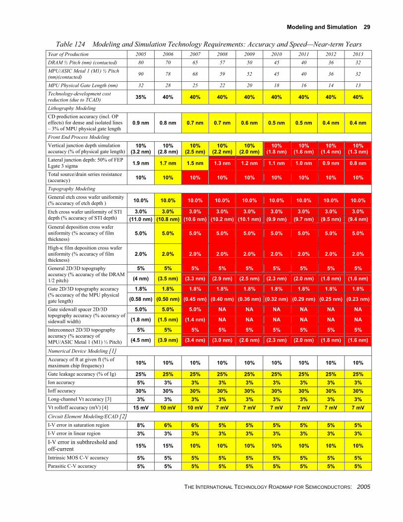
Modeling and Simulation 29
Table 124 Modeling and Simulation Technology Requirements: Accuracy and Speed—Near-term Years Year of Production 2005 2006 2007 2008 2009 2010 2011 2012 2013 DRAM ½ Pitch (nm) (contacted) 80 70 65 57 50 45 40 36 32 MPU/ASIC Metal 1 (M1) ½ Pitch (nm)(contacted) 90 78 68 59 52 45 40 36 32
MPU Physical Gate Length (nm) 32 28 25 22 20 18 16 14 13 Technology-development cost reduction (due to TCAD) 35% 40% 40% 40% 40% 40% 40% 40% 40%
Lithography Modeling CD prediction accuracy (incl. OP effects) for dense and isolated lines – 3% of MPU physical gate length
0.9 nm 0.8 nm 0.7 nm 0.7 nm 0.6 nm 0.5 nm 0.5 nm 0.4 nm 0.4 nm
Front End Process Modeling Vertical junction depth simulation accuracy (% of physical gate length)
10% (3.2 nm)
10% (2.8 nm)
10% (2.5 nm)
10% (2.2 nm)
10% (2.0 nm)
10% (1.8 nm)
10% (1.6 nm)
10% (1.4 nm)
10% (1.3 nm)
Lateral junction depth: 50% of FEP Lgate 3 sigma 1.9 nm 1.7 nm 1.5 nm 1.3 nm 1.2 nm 1.1 nm 1.0 nm 0.9 nm 0.8 nm
Total source/drain series resistance (accuracy) 10% 10% 10% 10% 10% 10% 10% 10% 10%
Topography Modeling General etch cross wafer uniformity (% accuracy of etch depth ) 10.0% 10.0% 10.0% 10.0% 10.0% 10.0% 10.0% 10.0% 10.0%
3.0% 3.0% 3.0% 3.0% 3.0% 3.0% 3.0% 3.0% 3.0% Etch cross wafer uniformity of STI depth (% accuracy of STI depth) (11.0 nm) (10.8 nm) (10.6 nm) (10.2 nm) (10.1 nm) (9.9 nm) (9.7 nm) (9.5 nm) (9.4 nm) General deposition cross wafer uniformity (% accuracy of film thickness)
5.0% 5.0% 5.0% 5.0% 5.0% 5.0% 5.0% 5.0% 5.0%
High-κ film deposition cross wafer uniformity (% accuracy of film thickness)
2.0% 2.0% 2.0% 2.0% 2.0% 2.0% 2.0% 2.0% 2.0%
5% 5% 5% 5% 5% 5% 5% 5% 5% General 2D/3D topography accuracy (% accuracy of the DRAM 1/2 pitch) (4 nm) (3.5 nm) (3.3 nm) (2.9 nm) (2.5 nm) (2.3 nm) (2.0 nm) (1.8 nm) (1.6 nm)
1.8% 1.8% 1.8% 1.8% 1.8% 1.8% 1.8% 1.8% 1.8% Gate 2D/3D topography accuracy (% accuracy of the MPU physical gate length) (0.58 nm) (0.50 nm) (0.45 nm) (0.40 nm) (0.36 nm) (0.32 nm) (0.29 nm) (0.25 nm) (0.23 nm)
5.0% 5.0% 5.0% NA NA NA NA NA NA Gate sidewall spacer 2D/3D topography accuracy (% accuracy of sidewall width) (1.8 nm) (1.5 nm) (1.4 nm) NA NA NA NA NA NA
5% 5% 5% 5% 5% 5% 5% 5% 5% Interconnect 2D/3D topography accuracy (% accuracy of MPU/ASIC Metal 1 (M1) ½ Pitch) (4.5 nm) (3.9 nm) (3.4 nm) (3.0 nm) (2.6 nm) (2.3 nm) (2.0 nm) (1.8 nm) (1.6 nm)
Numerical Device Modeling [1] Accuracy of ft at given ft (% of maximum chip frequency) 10% 10% 10% 10% 10% 10% 10% 10% 10%
Gate leakage accuracy (% of Ig) 25% 25% 25% 25% 25% 25% 25% 25% 25% Ion accuracy 5% 3% 3% 3% 3% 3% 3% 3% 3% Ioff accuracy 30% 30% 30% 30% 30% 30% 30% 30% 30% Long-channel Vt accuracy [3] 3% 3% 3% 3% 3% 3% 3% 3% 3% Vt rolloff accuracy (mV) [4] 15 mV 10 mV 10 mV 7 mV 7 mV 7 mV 7 mV 7 mV 7 mV Circuit Element Modeling/ECAD [2] I-V error in saturation region 8% 6% 6% 5% 5% 5% 5% 5% 5% I-V error in linear region 3% 3% 3% 3% 3% 3% 3% 3% 3% I-V error in subthreshold and off-current 15% 15% 10% 10% 10% 10% 10% 10% 10%
Intrinsic MOS C-V accuracy 5% 5% 5% 5% 5% 5% 5% 5% 5% Parasitic C-V accuracy 5% 5% 5% 5% 5% 5% 5% 5% 5%
THE INTERNATIONAL TECHNOLOGY ROADMAP FOR SEMICONDUCTORS: 2005

30 Modeling and Simulation
Year of Production 2005 2006 2007 2008 2009 2010 2011 2012 2013 DRAM ½ Pitch (nm) (contacted) 80 70 65 57 50 45 40 36 32 MPU/ASIC Metal 1 (M1) ½ Pitch (nm)(contacted) 90 78 68 59 52 45 40 36 32
MPU Physical Gate Length (nm) 32 28 25 22 20 18 16 14 13 Accuracy of Gm and Gd at Vt +150mV versus L, Vbs, Vds and T 10% 10% 10% 10% 10% 10% 10% 10% 10%
Circuit delay accuracy (% of 1/maximum chip frequency) 5% 5% 5% 5% 5% 5% 5% 5% 5%
RLC delay accuracy (% of 1/maximum chip frequency) 5% 5% 5% 5% 5% 5% 5% 5% 5%
Package Modeling Package delay accuracy (% of 1/off-chip clock frequency) 1% 1% 1% 1% 1% 1% 1% 1% 1%
Temperature distribution for package (accuracy) 1C 1C 1C 1C 1C 1C 1C 1C 1C
Numerical Method Speed-up of algorithms for 3D process/device/interconnect simulation (compared with year 2000)*
8× 11.2× 16× 22.4× 32× 45x 64x 90x 128x
*Numbers referring to continuum models. Estimated scaling similar to the ITRS. Different figures expected for other models.
Manufacturable solutions exist, and are being optimized Manufacturable solutions are known
Interim solutions are known Manufacturable solutions are NOT known
Notes for Table 124: [1] In Numerical Device Modeling equations are solved which are typically based on fundamental physics and describe the electrical behavior on spatially fine resolved quantities. This means usually partial differential equations (with respect spatial coordinates) are employed. The goal is technology optimization and device insight. [2] In Circuit Element Modeling no spatially resolved models are used. Approximatively analytically solveable, physically based models give a guidance for the used relations between electrical quantities. The goal is a description of device behaviour (currents, charges, noise) in circuit simulators. [3] Absolute values strongly differ for HP and LSTP. Important aspects for nominal devices also included in rolloff accuracy [4] (Positive) difference in Vth of nominal and subnominal device
REFERENCES The most recent version of other roadmaps including some future Modeling and Simulation topics for semiconductors is the iNEMI Technology Roadmap 2004 produced by the International Electronics Manufacturing Initiative1. Although the Technology Roadmap for Nanoelectronics2 produced by the European Commission’s IST programme (Future and Emerging Technologies) was already published in 2000 it still contains relevant information. Simulation issues addressed in the iNEMI roadmap are largely related to systems and products and therefore focus on reliability, electrical, and thermal simulation, furthermore on optoelectronics, microelectromechanical systems, and nanoscale/spintronics. The EU Nanoelectronics Roadmap elaborates especially on emerging devices beyond CMOS and the nanofabrication techniques needed for them. Whereas this gives relevant information for simulation on the long-term scale, molecular modeling is described in some detail. The working group received contributions to its discussion from the European Specific Support Action “SUGERT”3, funded by the European Commission within the IST programme. SUGERT focuses on specifications and promotion of R&D actions in the area of TCAD. These three external activities well complement each other.
1 See http://www.inemi.org. 2 R. Compano, ed. Technology Roadmap for Nanoelectronics. Second Edition. November 2000, see http://www.cordis.lu/ist/fet/nidqf.htm. 3 See http://www.iisb.fraunhofer.de/en/arb_geb/sugert.htm.
THE INTERNATIONAL TECHNOLOGY ROADMAP FOR SEMICONDUCTORS: 2005

Modeling and Simulation 31
INTER-ITWG ISSUES
Whereas cross-cut links between Modeling and Simulation and the focal ITWGs are summarized in the chapters of those ITWGs, strong links also exist to the other cross-cut ITWGs, as explained in the following sub-sections.
LINKS BETWEEN MODELING AND SIMULATION AND ENVIRONMENT, SAFETY AND HEALTH For the optimization of ESH issues, the elementary chemical reactions in each relevant process must be understood as far as possible, and new measurement and evaluation methods must be implemented for developing processes which have the lowest ESH impact. Similarly, availability of these measurement methods and knowledge of the reactions is also a key requirement for the development of predictive models for those processes, which are dealt with in the Modeling and Simulation chapter. In turn, many enabling measurement techniques can be shared between ESH and the Modeling and Simulation community, although the final targets of the two areas are different: Assessment of material consumption and occurance of hazardous species for ESH versus the geometry, doping and morphology of layer stacks in Modeling and Simulation. Moreover, the implementation of such models in equipment simulation programs, especially for plasma processes, also offers the possibility to ESH to obtain quantitative data for the generation of hazardous species and in the ideal case also for optimization of equipment and process conditions to minimize the generation of these species or their release from the process equipment. Moreover, simulation can frequently contribute to characterization techniques by converting measured data (like spectra) into quantitative data (for example, on gas composition). See the cross-cuts with Metrology. In this way ESH and Modeling and Simulation have the potential to support each other well.
Also Modeling and Simulation is requested to respond to the “Design for Environment, Safety, and Health” near-term ESH challenge. It is not sufficient to limit the impact of simulation to the replacement of a certain numbers of wafers during process development and optimization, which saves costs and (partly ESH-relevant) resources. Moreover, simulation should also contribute to the reduction of resources including critical chemicals during production, by minimizing deposited wafer thicknesses, material removal in CMP, and the frequency of cleaning processes to the amount really needed to achieve the desired result in terms of device and IC performance and reliability. To this end not only appropriate modes and simulation tools must be available, similar to the requests by the other chapters, but also resource conservation must be introduced as an additional target figure and metric for simulation.
LINKS BETWEEN MODELING AND SIMULATION AND YIELD ENHANCEMENT Besides the standard use of Modeling and Simulation to reduce development times and costs, links between Yield Enhancement and Modeling and Simulation are twofold: First, Modeling and Simulation can contribute to the assessment of the influence of defects on the ICs. An obvious example is the question whether mask defects of a specific size, kind, and position are printed during an optical lithography and subsequent etching steps. This can be studied by state-of-the-art simulation tools for optical lithography, which also allows identification of critical defect sizes above which the device or IC is destroyed, for example because the defect will cause otherwise separate lines to be connected. Especially for the investigation of defect limits for patterning steps simulation offers very good prospects provided the simulation tools are further developed accordingly. The propagation of defects in subsequent process steps through to devices and ICs and the mutual interactions of defects can be studied with various other Modeling and Simulation tools to monitor and minimize their impact.
Another important problem is the assessment of the impact of largely inevitable process fluctuations on the performance of devices and ICs. Many parameters in a fabrication line are distributed around their nominal values with some tolerances, like anneal temperatures, times, and ramp profiles, or have some drift in time. Advanced Process Control (APC) is used to reduce the impact of such fluctuations by feeding metrology data back into process recipes. Control models are largely based on silicon data that is expensive to generate and might be available for mature processes only. Coupled process and device simulations can help to develop more accurate APC models in shorter time. By using process and device models calibrated in the process integration phase, APC models can already be developed for process transfer and production ramp up.
A second method addressing the problem of process fluctuations uses coupled process and device simulation to calculate the spread of critical product parameters resulting from such distributions of fabrication parameters. Using this method statistical SPICE models can be derived before statistical fabrication data is available, and in this way contribute to the early assessment and optimization of the yield for a specific product and fabrication technology.
THE INTERNATIONAL TECHNOLOGY ROADMAP FOR SEMICONDUCTORS: 2005

32 Modeling and Simulation
Obviously, these contributions from Modeling and Simulation to Yield Enhancement require sufficient generality, accuracy, and speed of application of the simulation tools to be used, and are a challenge for the future development of Modeling and Simulation.
LINKS BETWEEN MODELING AND SIMULATION AND METROLOGY Strong bi-directional links exist between Metrology and Modeling and Simulation. A key issue in the development of physical models for semiconductor fabrication processes and equipment as well as devices is the availability of measurement techniques and methodologies that are capable of characterizing quantities such as geometry and chemical composition of layer stacks, dopant distributions, (point) defects, stress/strain, carrier concentrations, lifetime and mobility with the high accuracy and spatial resolution, and low detection limit required to enable model development and evaluation. Metrology is needed that gives sufficient information for true three-dimensional structures. In many cases it must be applicable to real structures rather than test structures designed for that specific purpose. A further complication results from the required measurement and model accuracy approaching or even getting lower than the distance between individual (dopant) atoms. In these cases the interpretation of measurement results becomes questionable, whereas in simulation the transition from continuum models based on partial differential equations to atomistic calculations is being accomplished.
The requirements of Modeling and Simulation contribute to driving the development of Metrology. However, simulation not only raises requirements but also can and must contribute to the development and use of metrology itself. The physical understanding of the processes occurring in the semiconductor and other materials considered is in many cases extremely valuable to interpret data collected in metrology and to convert them into quantitative information, to give realistic error estimates, and even to design or customize a measurement method. For example, simulation can be used to relate variations of process parameters or atomic fluctuations to spreads of quantities that are measured, and in this way help to correctly interpret measurements. Some other examples are the use of simulation to support and complement mask metrology, scatterometry, and the application of metrology for APC.
Frequently Modeling groups directly contribute to the development and customization of measurement methodologies required to provide the data needed for model development. For example, with the increasing variety of new materials and processes in gate etch processes and complexity of gases and materials involved in dielectric etch and process cleans, simulation is called for creating a reliable means to characterize process emissions. In most cases, what evolves from surfaces or in the gas phase is unknown or difficult to synthesize outside of the particular process set-up and equipment. An emerging means of identifying species of potential environmental risk is through computational spectra generation. Synthetic reference spectra for materials can be generated with relative ease using computational chemistry approaches. For example, FTIR (Fourier-Transform Infrared Spectroscopy) spectra have been used to identify radicals of the RuOx system in Ruthenium etch processes and to scan for noxious gases to ensure they are not produced in highly polymerizing dielectric etch gas chemistries. In both these cases, experimental reference spectra are difficult to generate or difficult to obtain.
Furthermore, it is frequently possible to verify simulation models and tools using measurement methods available (such as 2D measurement of cross sections), and then to use them beyond the domain directly accessible to measurement techniques (for example, for 3D profiling) because in that cases the physics has not changed and the difference between the two situations can reliably be handled by the algorithms in the simulator (solving partial differential equations in three instead of two dimensions). To conclude, Metrology and Modeling and Simulation must continue to cooperate closely to take best advantage from each other.
THE INTERNATIONAL TECHNOLOGY ROADMAP FOR SEMICONDUCTORS: 2005