experimental optimization of decoupling capacitors in fpga ... · experimental optimization of...
TRANSCRIPT

DesignCon 2012
Experimental Optimization ofDecoupling Capacitors in FPGADesigns by On-Die Measurementof Power Distribution ImpedanceFrequency Profile
Cosmin Iorga, Ph.D., [email protected] (805) 231-9786

2
Abstract
On-die measurement of power distribution network (PDN) impedance frequency profileof field programmable gate arrays (FPGA) is performed by configuring and using onlylogic blocks commonly available in any existing FPGA, without built-in dedicatedcircuits. All measurements are done inside the FPGA without the need of externalinstruments. A case study implementation in a Spartan 3A FPGA has been able tomeasure the PDN impedance frequency profile at frequencies up to 500MHz and hasidentified resonance peaks not seen by board level measurements. Further application toa PDN design has been able to optimize a trade-off between placement of decouplingcapacitors and PCB manufacturing cost reduction, to help identify that the intendedFPGA core clock frequency of 200MHz was too close to a PDN resonance peak at220MHz, and to help locate a minimum PDN impedance at 320MHz where the FPGAclock has been set to operate. All these PDN improvements have not been possible withonly board level PDN impedance measurements since the dominant contributors were thePDN interconnects on FPGA die and package.
Author Biography
Dr. Cosmin Iorga is the founder of NoiseCoupling.com and has accumulated over 20years of experience in high-speed circuit design and troubleshooting at system, board,and integrated circuit levels, with emphasis on signal integrity, power integrity, and noisecoupling reduction. Cosmin has earned his Ph.D. in electrical engineering from StanfordUniversity, and he has filed more than 15 patents with 9 granted so far, coveringinnovative solutions in noise coupling reduction and signal integrity. Cosmin is theauthor of the book “Noise Coupling in Integrated Circuits: A Practical Approach toAnalysis, Modeling, and Suppression”.

3
1. Introduction
Field programmable gate arrays (FPGA) are integrated circuits that can beprogrammed by users to perform customized logic functions. In a typical design processa user defines customized logic functions using a computer aided design software tool,such as schematic capture or hardware description language (HDL). The software toolthen implements the design for a specified programmable logic device type usingconfigurable logic block resources available on that device. The implemented design isstored in a configuration data file. This file is then loaded into a programmable logicdevice (PLD), configuring the PLD to perform the customized logic functions.
An FPGA is typically mounted on a printed circuit board (PCB) as part of anelectronic system. Multiple voltage regulator modules (VRM) mounted on the PCBprovide power supply to the FPGA internal circuits. The electric circuit comprising thevoltage regulator, the interconnects from the voltage regulator to the on-die circuits of theprogrammable logic device, and decoupling capacitors is called power distributionnetwork or power delivery network (PDN).
Typical FPGAs are fabricated in complementary metal-oxide-semiconductor(CMOS) process. In digital circuits fabricated in CMOS process when a signaltransitions from a logic state “false” to a logic state “true” a transient electric currentflows from the positive node of the power supply into the digital circuit. Similarly whena signal transitions from a logic state “true” to a logic state “false” a transient electriccurrent flows from the digital circuit into the negative node of the power supply. Thesetransient currents flow through the power distribution network and generate transientvoltage drops on the electrical impedance of the power distribution components. As adirect consequence of transient voltage drops, the on-die positive voltage supply dropsmomentarily and the on-die negative voltage supply rises momentarily. The on-diecircuits see these momentary supply voltage drops and rises as power supply noise. Thisnoise is called switching noise because the switching of signal logic states in the digitalcircuits generates it.
1.1 Simultaneous Switching Noise in FPGAs
In a typical FPGAs multiple signals may switch at the same moment in timeincreasing the magnitude of switching noise on the positive and negative supplies. Thiseffect is commonly refereed to as simultaneous switching noise (SSN). Simultaneousswitching noise (SSN) degrade the performance of the FPGA circuits. The magnitude ofthe simultaneous switching noise (SSN) depends on the number of switching gates of theprogrammable logic device, the switching speed, and the electrical impedance of thepower distribution network (PDN). In recent years a lot of effort has been made to designlow impedance power distribution networks for FPGA applications; for example [1]investigates the effectiveness of FPGA power distribution in the package, and [2]presents the challenges of designing a PDN system in a FPGA-based system.
In general, the power distribution network impedance is a complex quantityhaving the magnitude dependent on frequency. As a direct consequence, the magnitude of

4
simultaneous switching noise depends on the frequency of operation of the FPGA. Mostpower distribution networks present impedance magnitude peaks at some frequencies,called resonance peaks. If the operating frequency of the FPGA, or harmonics of theoperating frequency, overlap with a resonance peak of the power distribution network,then significant noise is generated on the on-die voltage supplies.
Knowing the frequency characteristics of the power distribution impedance canhelp reduce the simultaneously switching noise by configuring the programmable logicdevice to operate at frequencies that do not overlap with the resonance peak frequencies.Alternately, designers can modify the power distribution network circuit so that theresonance peaks do not overlap with operating frequencies or their harmonics, which istypically done through adjusting the values of decoupling capacitors. Many timesoptimization of power distribution is needed to insure proper functionality of the FPGAcircuits; [3] describes package optimization for achieving cost performance balance, and[4] describes optimization to reduce leakage of FPGA on-die decoupling capacitors.
It is therefore desirable to know the frequency characteristic of the powerdistribution impedance. A lot of effort has been made in recent years to developtechniques for modeling, simulating, and measuring the impedance and noise of powerdistribution networks.
Simulation of power distribution networks in FPGA applications has beenreported in [5] covering effects of simultaneously switching noise, and in [6] covering themodeling of power and ground in FPGA applications. Most commercial software toolsfocus on modeling and simulation of general Application Specific Integrated Circuits(ASIC). While these tools may be accurate for custom designs, in FPGA applications theinformation about on-die circuits and package is not completely available from vendors,and thus approximations are made, which reduce the effectiveness of the model and theaccuracy of the simulation results.
1.2 PDN Impedance Measurement
Measurement techniques typically cover only the section of the power distributionimpedance on the printed circuit board, and do not address the sections of the interface topackage, in the package, of the interface to die, and in the die. While measurements ofthe printed circuit board can be very accurate, many times some of the resonance peakfrequencies change when the package with die is attached to the board. Therefore, on-diemeasurement techniques can provide more accurate results. Typical on-die measurementtechniques use built-in dedicated circuits that measure the power distribution networkimpedance, as exemplified in [7]. These built-in measurement circuits have to beimplemented during the fabrication of integrated circuits, and most field programmablegate array (FPGA) devices available on the market do not have such built-in circuits. Typical FPGA PDN design approach uses design guidelines from FPGA vendors[8], [9]; however, while this is a simple and inexpensive solution, in some applicationsthe results may not be satisfactory since the transient currents generated by FPGA circuitsdepend on the specific system and functions programmed by users in the FPGA and mayrequire further optimization of the power distribution network beyond the resultsobtained using vendor guidelines.

5
A more efficient design may be obtained by using PDN design graphical softwaretools provided by some vendors. For example Altera provides a dedicated PDN softwaretool for their families of FPGAs [10]. The PDN design process sets a target PDNimpedance based on estimated switching noise signature and various parameters of thepower distribution network on PCB. Many times additional modeling and simulationtools are needed to determine the PDN parameters on the PCB.
More sophisticated simulations use commercial tools and design parameters ofPDN on die, package, PCB, and interface connections. While these simulations mayprovide more accurate results, they depend on design parameters of the FPGA die andpackage, which are not easily available from FPGA manufacturers.
This paper presents a method of experimentally optimizing the power distributionnetwork (PDN) in field programmable gate array (FPGA) applications by implementingon-die measurement of power distribution impedance using only logic blocks commonlyavailable in any existing FPGA, without the need of any built-in dedicated circuits. Allmeasurements are done inside the FPGA without the need of external instruments. Thismethod can be implemented in most existing FPGA devices to select decouplingcapacitors or to troubleshoot PDN issues in existing systems, after which the FPGA maybe reconfigured to perform any other user-defined functions.
2. Differences between PDN Impedance On-Die and On-PCB
A common technique for determining the impedance of a network in AC steady-state analysis consists of applying a test AC current source to a network port that injectsan AC current into the network, as shown by I_SIN in Figure 1, and measuring theinduced AC voltage on that network port, as illustrated by V_SIN in the figure.
Figure 1. Power distribution impedance analysis using AC steady-state method

6
The impedance is then calculated as the measured voltage divided by the injectedcurrent. To determine the PDN impedance as seen by the circuits on the die, Z_PDN_DIEin the figure, the AC current source has to be placed on the die as shown by I_SIN.Many times due to accessibility limitations the analysis is performed only at PCB level.In these cases the measured impedance, Z_PDN_PCB, represents the PDN impedance ofonly the circuit components on the PCB. There may be significant differences betweenZ_PDN_DIE and Z_PDN_PCB, as illustrated by the example in Figure 2. The bluecolored trace represents the PDN impedance measured on the PCB with empty socket(without FPGA), and the pink colored trace represents the same PDN impedance on PCBafter soldering the FPGA. The difference at high frequencies comes from the additionalinductance and decoupling capacitance in the FPGA package and die.
If we were able to place an AC source on the FPGA die we could determine thePDN impedance as seen by the circuits on die, as illustrated by the black colored trace(with no decoupling capacitors on the package) and red colored trace (with decouplingcapacitors on the package). The first difference that we observe is the resistive shift ofthe on-die PDN traces, which is mainly caused by the resistance of interconnects in thepackage, bond-wires or die bumps, and power grid in the die. It can also be noticed thatthe decoupling capacitance on package lowers the PDN impedance at frequencies higherthan 100MHz but also creates a resonance peak at around 60MHz. This resonance peakcan be seen on the PCB measured PDN impedance trace but its magnitude is lower thanthe magnitude seen by the circuits on the die.
Figure 2. Example of power distribution impedance frequency characteristic as seen from the die and fromthe PCB with and without decoupling capacitors on the package
In calculations and simulations, the AC steady-state analysis uses linearizedmodels of the devices present in the network, thus the value of the injected current doesnot affect the measured impedance. When implementing this method to live circuits we

7
need to make sure that the injected current is sufficiently small so that it does not affectsignificantly the operating points of non-linear devices, keeping them within the smallsignal approximation used in AC circuit analysis.
3. AC Steady-State Analysis Implemented in FPGAs
In order to use the AC steady-state analysis impedance measurement method inFPGA applications, we need to apply an AC current source to a power distributionnetwork port and we need to measure the resulting AC voltage on that power distributionnetwork port. Both the AC current source and the AC voltage measurement have to beimplemented on the FPGA die. While technically it is possible to design on-diespecialized circuits when FPGAs are manufactured, these specialized circuits are not soconvenient to implement because they may take significant area of the die and mayincrease the cost of FPGA devices. To be applicable to any existing FPGA device, theproposed method uses only common logic blocks available in any typical FPGA device.
Figure 3 shows a block diagram of a power distribution measurement systemimplemented in an FPGA by using only commonly available configurable logic blocks(CLB).
Figure 3. Block diagram of a power distribution measurement system implemented in an FPGA byconfiguring only commonly available logic blocks
Part of the FPGA internal logic blocks are configured to function as a currentsource that consumes a sinusoidal current from the on-die power supply voltage. Thissinusoidal current source has programmable frequency and an activate/deactivate feature.

8
When the current source is activated, a sinusoidal current flows through the powerdistribution network impedance and generates a sinusoidal variation of the on-die powersupply voltage. The sinusoidal current is obtained by summing the dynamic loadcharging and discharging currents of multiple CMOS gates, built as part of CLB blocks.Another group of configurable logic blocks in the FPGA is configured to form a ringoscillator, which is powered from the same on-die voltage supply as the sinusoidalcurrent source. The sinusoidal variation of the voltage supply modulates the frequencyof the ring oscillator, as illustrated in Figure 4.
Figure 4. The sinusoidal variation of the on-die voltage supply rail modulates the frequency of the ringoscillator
The upper trace shows the ring oscillator frequency in the absence of injectedsinusoidal current. The middle trace shows the sinusoidal variation of the on-die voltagesupply rail due to the sinusoidal current injected into the power distribution network. Thelower trace shows the frequency modulation produced by the voltage supply sinusoidalvariation on the ring oscillator circuit.
A frequency counter, configured also from configurable logic blocks of theFPGA, measures the steady-state average frequency of the ring oscillator signal over aperiod of time with and without the sinusoidal current source active. The electricalimpedance of the power distribution network is then calculated using a mathematicalformula involving the two measured average frequencies and functional specifications ofthe FPGA device. A simplified version formula could be: Z_PDN = [(f_mod –f_nom)/f_nom] x VDD / I_SIN, where Z_PDN is the power distribution impedance,f_nom is the ring oscillator frequency without injected AC current source I_SIN, f_modis the average frequency with AC injected current, VDD is the nominal supply voltage,and I_SIN is the magnitude of the injected current.
By repeating this measurement at multiple frequencies of the sinusoidal currentsource, a frequency characteristic (frequency profile) of the power distribution impedancecan be generated.

9
4. PDN Optimization
4.1 Background
Simplistic design processes use only manufacturers’ provided FPGA powerdistribution design tools to determine the number and values of decoupling capacitorsneeded. More involved design processes model and simulate the power distributionnetwork on the PCB and use the results together with manufacturers’ provided FPGApower distribution design tools. In more advanced product development flows, models ofPDN impedance on the FPGA package and die are included; however, this information istypically not easily available from FPGA vendors, and many times approximations andestimations have to be made. After the board is fabricated and assembled measurementsof power distribution impedance frequency profile are typically performed using a VectorNetwork Analyzer to determine if the impedance is below a target value over thefunctional frequency bandwidth. Decoupling capacitors are then adjusted as needed toachieve PDN impedance below the specified target.
4.2 Proposed Technique
While the existing optimization methods provide good results, they typicallyrequire extensive modeling and simulation time and sometimes expensive simulationsoftware and bench measurement instruments. In cases when time and cost become anissue the following proposed method can be used to optimize the power distributionnetwork.
The proposed technique uses an experimental approach instead of the traditionalmodeling and simulation approach. The PCB is designed with capacitor pads placed nearthe FPGA footprint on top and bottom sides of the PCB. For PCBs with BGA packagesand blind vias, capacitor pads are placed on the bottom side of the PCB under the FPGAland pattern. Additional pads for electrolytic or tantalum decoupling capacitors areplaced nearby as placement of other components allows.
During PCB assembly “best guess values” capacitors are placed on some of thepads. The FPGA is then programmed with the PDN measurement system bit file and theon-die PDN impedance frequency characteristic is measured. This frequencycharacteristic is used to estimate the supply noise based on dI/dt estimated switchingactivity of the functional design. Typically, the maximum supply noise occurs atresonant peaks. Capacitors are then chosen through an iterative experimental procedureby soldering them to the existing pads and measuring the on-die FPGA powerdistribution impedance. Depending on experimental measurements not all pads willneed to be stuffed with decoupling capacitors, and expensive high resonance frequencycapacitors may be decided that do not really help reduce the on-die PDN impedance andtherefore are not needed.

10
5. Case Study
In a case study, this proposed on-die measurement method has been implementedin a Spartan 3A FPGA on a test board. The method has been able to measure the PDNimpedance frequency profile at frequencies up to 500MHz. The case study goal was todesign the power distribution network in a new application based on an existing testboard implementing a Spartan 3A FPGA in a ball-grid-array (BGA) package. Newdesign had FPGA core clock operating at 200MHz, core power supply maximumswitching current of 0.8A with an estimated 15% overall activity factor and 30% clockfrequency activity factor.
5.1 Implementation of PDN Measurement Method
The on-die PDN measurement system, as previously illustrated in the blockdiagram of Figure 3, has been implemented in the Spartan 3A FPGA using Xilinx ISEdesign environment. Figure 5 shows the top level schematic diagram of the PDNmeasurement system.
Figure 5. Top level schematic diagram of the PDN measurement system implemented in a Spartan 3AFPGA using Xilinx ISE design environment
FPGA Clock Distribution Block
PDN Measurement Block

11
The measurement block, testip1, is clocked by a 256MHz signal provided by theclock module DCM_SP, and has a 4-bit serial interface connected to FPGA IO pads. Thissystem has been compiled into a bit programming file that has been further loaded intothe Spartan 3A FPGA. The device utilization, shown in Figure 6, is enough low to allowin some cases this PDN measurement block to be implemented together with the normalfunctionality circuits of the FPGA.
Figure 6. Device utilization table of the PDN measurement system implemented in a Spartan 3A FPGAusing Xilinx ISE design environment
In applications with high device utilization where it is not possible to implementthe PDN measurement block together with functional blocks, the PDN measurementsystem can be temporarily loaded only for optimizing the power distribution networkafter which it can be removed and the FPGA programmed with the functional applicationbit file.
The serial interface has been connected to a computer through a USB port and aninterface module. A Visual Basic application running on the computer has controlled thesinusoidal current generator and the frequency measurement block.
5.2 Experimental Optimization of Decoupling Capacitors
Figure 7 shows the bottom side of the PCB region underneath the FPGA, asmarked by the yellow square. Decoupling capacitors open pads are labeled C39, C43,C44, C45, and C50 in the figure.

12
Figure 7. Photograph showing the bottom side of the PCB region underneath the FPGA device marked bythe yellow square, and open decoupling capacitor pads labeled C39, C43, C44, C45, and C50
With this experimental setup the PDN measurement system has been programmedin the Spartan 3A FPGA and the frequency characteristic of the on-die power distributionimpedance has been measured, as shown in Figure 8.
Figure 8. Experimentally measured on-die frequency characteristic of the power distribution impedance ofthe Spartan 3A FPGA

13
The FPGA on-die measured PDN impedance is around 145 mOhms up to100MHz with an inductive peak of 233 mOhms at 9MHz, another inductive peak of 170mOhms at 220MHz and a capacitive deep of 130 mOhms at 320MHz, after which it goesup inductively.
The dotted line represents the expected variation of PDN impedance at lowerfrequencies below the accuracy frequency limit of the proposed technique. This expectedPDN impedance is computed from the measured PDN impedance at zero frequency andthe capacitive slope of the dominant decoupling capacitor, which in this application is thetantalum capacitor. In general the accuracy frequency limit can be extended to lowerfrequencies if needed with the expense of increasing the measurement time.
Figure 9 shows the process of optimizing C45 value by successive measurementsof PDN impedance for various capacitors mounted on the PCB pad.
Figure 9. The process of experimental optimization of C45 value by successive measurement of PDNimpedance for various capacitors mounted on the PCB pad
The blue trace corresponds to a 1nF capacitor, the cyan trace to 22nF, magenta to 47nF,red to 100nF and black to 220nF. It can be noticed that increasing C45 beyond 220nF
1nF 22nF47nF100nF
220nF
14
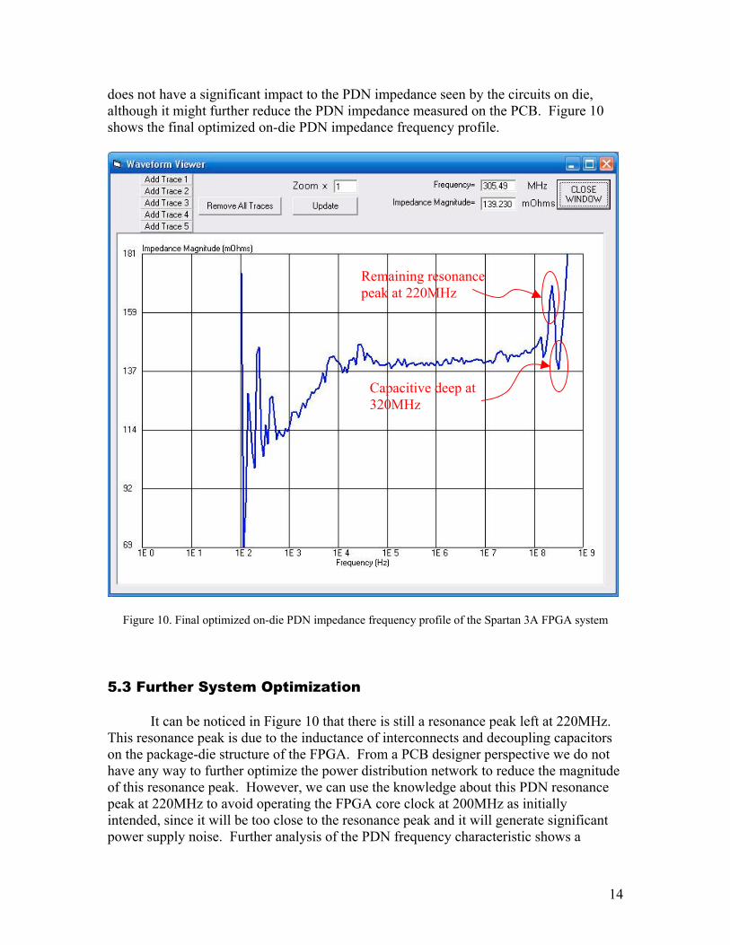
does not have a significant impact to the PDN impedance seen by the circuits on die,although it might further reduce the PDN impedance measured on the PCB. Figure 10shows the final optimized on-die PDN impedance frequency profile.
Figure 10. Final optimized on-die PDN impedance frequency profile of the Spartan 3A FPGA system
5.3 Further System Optimization
It can be noticed in Figure 10 that there is still a resonance peak left at 220MHz.This resonance peak is due to the inductance of interconnects and decoupling capacitorson the package-die structure of the FPGA. From a PCB designer perspective we do nothave any way to further optimize the power distribution network to reduce the magnitudeof this resonance peak. However, we can use the knowledge about this PDN resonancepeak at 220MHz to avoid operating the FPGA core clock at 200MHz as initiallyintended, since it will be too close to the resonance peak and it will generate significantpower supply noise. Further analysis of the PDN frequency characteristic shows a
Remaining resonancepeak at 220MHz
Capacitive deep at320MHz

15
minimum deep at 320MHz, so using a 320MHz clock will be a better choice from thesupply noise generation perspective.
One additional task of the new design was to investigate the effect of eliminatingblind vias underneath the FPGA to reduce cost. By using full vias, the decouplingcapacitors underneath the FPGA will have to be moved outside the FPGA contourmarked with the yellow line in the PCB layout shown in Figure 7. Experimentalremoving of C39, C43, C44, and C50 capacitors underneath the FPGA BGA package,resulted in the on-die PDN impedance showing a resonance peak at 32MHz of164mOhms, as shown by the red colored trace in Figure 11.
Figure 11. PDN impedance frequency profile with experimental removing of C39, C43, C44, and C50capacitors underneath the FPGA BGA package and with 200pH inductance added to the mounting pad of
each capacitor
Keeping the capacitors but moving them outside the BGA region could eliminate theblind vias but would add about 200pH to the mounting inductance. To evaluate how this additional inductance affects the on-die PDN impedance,about 200pH inductance has been added to the test board by lifting the capacitors andinserting wire jumpers. On-die measured PDN impedance showed that the inductive
Capacitors removed
Capacitors with addedmounting inductance

16
resonance peak at 32Mhz has lowered to148 mOhms, as shown by the black colored tracein Figure 11. Based on this study the new design can have the capacitors moved outsidethe BGA region, PCB without blind vias, and FPGA core clock frequency shifted from200MHz to 320MHz where the PDN impedance has a minimum deep.
6. Conclusion
In conclusion, the FPGA on-die PDN impedance measurement helped decide thetrade-off between placement of decoupling capacitors and PCB manufacturing costreduction, helped identify that the intended FPGA core clock frequency of 200MHz wastoo close to a PDN resonance peak at 220MHz, and helped locate a minimum PDNimpedance at 320MHz where the FPGA clock has been set to operate. All these PDNimprovements have not been possible with only on-board PDN impedance measurementssince the significant contributors were the PDN interconnects and decoupling capacitorson the FPGA package and die. This proposed method can configure any existing FPGAto measure on-die its power distribution impedance frequency profile, without usingbuilt-in dedicated circuits or external measurement instruments. In a productdevelopment flow this PDN optimization technique may shorten the schedule and reducethe overall cost by providing an alternate solution to expensive modeling and simulationsoftware tools and expensive test bench instrumentation.
References
[1] Wai Ling Lee; Hoon Ngik Low; Hong Shi, Bayan Lepas, Malaysi, “Investigation toeffectiveness of design factors for FPGA package PDN networks”, 11th ElectronicsPackaging Technology Conference, 2009, pp 107 – 112
[2] Yu Huimin; Fang Guangyou, “Power Distribution System Design for a FPGA-BasedGround-Penetrating Radar Receiver:, Power and Energy Engineering Conference, 2009.APPEEC 2009. Asia-Pacific, pp 1 – 4
[3] Zhuyuan Liu; Shishuang Sun; Boyle, P., “FPGA core PDN design optimization”,IEEE International Symposium on Electromagnetic Compatibility (EMC), 2011, pp 411 –416
[4] Vaidyanathan, B.; Srinivasan, S.; Yuan Xie; Vijaykrishnan, N.; Luo Rong, “LeakageOptimized DECAP Design for FPGAs”, IEEE Asia Pacific Conference on Circuits andSystems, 2006. APCCAS 2006, pp 960 – 963
[5] Hong Shi, Geping Liu; Alan Liu, Pannikkat, A., Kok Siang Ng, Yee Huan Yew,“Simultaneous switching noise in FPGA and structure ASIC devices, methodologies foranalysis, modeling, and validation”, 56th Electronic Components and TechnologyConference, 2006, Proceedings, pp 8

17
[6] Hong Shi, Xiaohong Jiang, Yeehuan Yew, “Effect of Power and Ground Co-Reference to Performance of Memory Interface I/Os in FPGA and Structural ASICDevice Packages”, 57th Electronic Components and Technology Conference, 2007,ECTC '07. Proceedings, pp 804 – 809
[7] Shishuang Sun, Larry D Smith, Peter Boyle, “On-Chip PDN Noise Characterizationand Modeling”, DesignCon 2010
[8] Altera AN 574: Printed Circuit Board (PCB) Power Delivery Network (PDN)Design Methodology
[9] Xilinx XAPP623: Power Distribution System (PDS) Design: UsingBuypass/Decoupling Capacitors
[10] Altera "PowerPlay Power Analysis Technology" PDN analysis tool, Altera'sQuartus II development software