grant agreement number - european commission :...
TRANSCRIPT
Grant Agreement Number: 224525
Project Acronym: NEMSIC
Project Title: Hybrid Nano-Electro-Mechanical / Integrated Circuit
Systems for Sensing and Power Management Applications
Funding Scheme: Collaborative project
Thematic Area: Information and Communication Technologies
Project start date: 01/06/2008
Deliverable D6.3: 2nd Update to the Plan for using and dissemination of foreground
Nature1: R
Dissemination level2: RE
Due date: Month: M46
Date of delivery: M46
Partners involved: EPFL, SCIPROM, HON, IMEC, IMEC-NL, SOU, CEA-LETI, All
Authors: Antonios Bazigos, Cornel Cobianu, Sywert Brongersma, Cécilia Dupré, Kirsten
Leufgen
Document version: 1
1 R = Report, P = Prototype, D = Demonstrator, O = Other
2 PU = Public, PP = Restricted to other programme participants (including the Commission Services, RE =
Restricted to a group specified by the consortium (including the Commission Services), CO = Confidential, only
for the members of the consortium (including the Commission Services)
NEMSIC: Grant Agreement n. 224525 Final Report – Final Version – July 2012
2
Revision history
Version Date Author Comment
0.1 01.09 Dimitrios Tsamados First issue
0.2 01.09 Paolo Dainesi Added EC compliant format and
comments
0.3 02.09 Cornel Cobianu Added HON contribution
0.4 23.02.09 Cornel Cobianu Added another HON contribution
0.5 27.02.09 Sywert Brongersma Included contribution form IMEC-
NL
0.6 10.07.09 Cécilia Dupré LETI Contribution
1 31.07.09 Kirsten Leufgen Completion and polish
2.0 25.08.10 Paolo Dainesi Added web site activities in year 2
3.0 04.06.12 Antonios Bazigos
Final Update: added details for the 2
workshops, web site update, journals,
conferences, patents.
NEMSIC: Grant Agreement n. 224525 Final Report – Final Version – July 2012
3
Table of Contents
Revision history ......................................................................................................................... 2
Executive Summary ................................................................................................................... 4
Introduction ................................................................................................................................ 4
Section A (public) - Dissemination of foreground..................................................................... 4
Dissemination activities carried out or confirmed .............................................................................. 5
Template A (Public) ..................................................................................................................... 21
Section B (confidential) - Use of foreground ........................................................................... 30
Template B2 (Confidential) .......................................................................................................... 32
Exploitable Foreground............................................................................................................ 34
NEMSIC: Grant Agreement n. 224525 Final Report – Final Version – July 2012
4
Executive Summary
The objective of this deliverable is to define the dissemination and exploitation of the project
results and products by the partners. Dissemination activities and strategies for the envisaged
scientific results of the project will include presentations to international conferences,
symposia and workshops as well as publications in peer-reviewed specialised scientific
journals. Vulgarised versions of some achievements and results of NEMSIC will be presented
to the general public through the dedicated web site (www.nemsic.org), as well as through
press releases and publications on the Internet or in magazines.
Each technical workpackage provides a list of the various dissemination events, which are
selected in order to provide the best visibility possible to the technological achievements
within the framework of the NEMSIC project and to match the level of the presentations to
the targeted audience.
Partners with strong commercial interests, especially Honeywell and IMEC-NL but also
CEA-LETI present also their exploitation plans, describing their interests in the project results
and how they intend to exploit them in future product development or technology licensing.
Introduction
The present report is to be considered as the “Plan for Use and Dissemination of Foreground”
which is due at the end of the project. As such it is an open document to which all partners
can contribute as soon as they have reached decisions concerning their exploitation strategy or
achieved dissemination activities. In the future years the document will be regularly updated
by all partners.
The text parts in italic and blue all along the document, reported from the “Guidance notes on
Project Reporting” of the European Commission, are intended as guidelines on how this
deliverable should be filled during the project duration and until its end.
Section A (public) - Dissemination of foreground
The dissemination plan extends up to the ending date of the project wherever that is possible,
but one has to note that updates are already envisaged for M18 and M36. In this report we
expect to have publishable results just before or right after the major milestones and the
deadlines of the deliverables in each workpackage.
The dissemination of the foreseeable scientific results has been organized by workpackage in
order to take into account the particularities of each WP (domains of research, different
milestones and dates of deliverables, more or less dependence on the technological steps and
risks).
NEMSIC: Grant Agreement n. 224525 Final Report – Final Version – July 2012
5
Dissemination activities carried out or confirmed
The dissemination activities already carried out or confirmed during the project duration are
the following:
The project presentation (D6.8) has been prepared as a collaborative work between EPFL
and SCIPROM. It is a general overview of the project written in journalistic style to
promote the project in different occasions. The presentation is available as a separate pdf
file and can be downloaded from the public area of the NEMSIC web-site.
At the very beginning of the project SOU has prepared a press release, which appeared on
their web-site as well as on the CORDIS new web-site and RSS feed.
See link:http://cordis.europa.eu/fetch?CALLER=EN_NEWS&ACTION=D&RCN=29617
The press release is also reported in the NEMSIC web-site news section. In the future
such actions will be taken by the project coordinator, in the name of all partners, when the
first significant results will be achieved by the consortium.
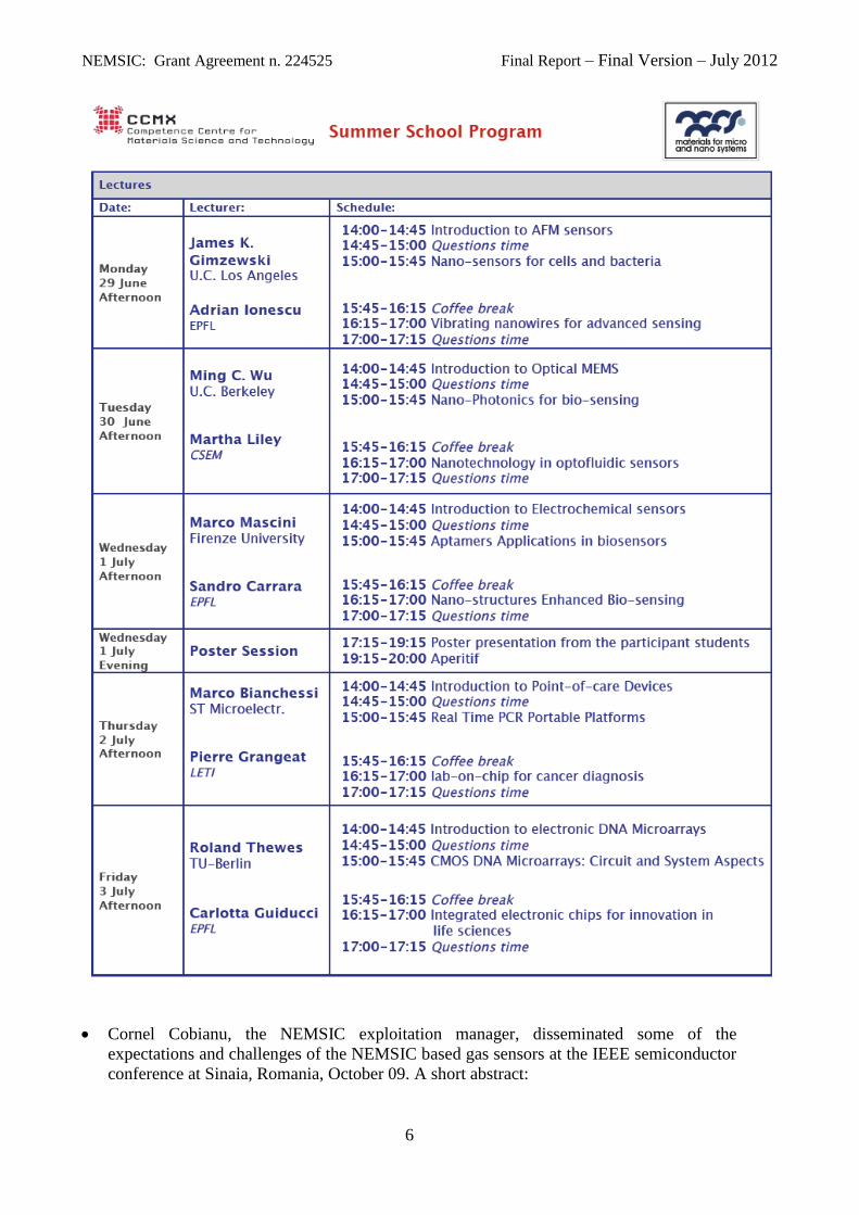
The NEMSIC coordinator, Prof. A.M. Ionescu, was invited to act as lecturer in an
international summer school organized by EPFL in June 09. His talk was about Vibrating
nanowires for advanced sensing and presented to international students the concepts of
NEMSIC versus state of the art in the field. The detailed program of this Summer school
is shown below:
NEMSIC: Grant Agreement n. 224525 Final Report – Final Version – July 2012
6
Cornel Cobianu, the NEMSIC exploitation manager, disseminated some of the
expectations and challenges of the NEMSIC based gas sensors at the IEEE semiconductor
conference at Sinaia, Romania, October 09. A short abstract:
NEMSIC: Grant Agreement n. 224525 Final Report – Final Version – July 2012
7
Nano-scale resonant sensors represent an emerging research domain built on
the foundation of micro-electro-mechanical systems, which are thus pushed to
their limits on size, technology and design and interrogation electronics. These
nano-devices are going to become the next generation of low power, low cost,
high sensitivity, ultra-miniaturized sensors for a new type of applications such
as large wireless sensor networks of the future. Even if today, they are mainly
in our imagination, at the level of mass detection, resonant nano-structures
have already proved a mass sensing resolution of a few zeptograms/Hz, in
ultrahigh vacuum and low temperature laboratory set-up. This is stimulating
the challenging expectation of ultra-high sensitivity in gas sensing, even if the
available sensing area is ultra-small and gases atoms to be detected are
“scarce” above that sensing surface. Starting from such intuitive thinking, it is
the purpose of our paper to describe requirements for the resonant structures to
become real resonant gas (NOT mass) sensors, of tomorrow. To reach there,
we think it is compulsory to get enhanced gas sensitivity and selectivity,
preserving high quality factor, high frequency, even if they have to operate in
“the field” at ambient pressure and temperature in the presence of a large
number of noise sources.
A paper presented by Cornel Cobianu was furthermore accepted for the CAS 2009
conference:
“Nano-Scale Resonant Sensors For Gas And Bio Detection: Expectations
And Challenges”, authors: C. Cobianu1, B. Serban
1, M. Mihaila
1, V. Dumitru
1,
F.A. Hassani2, Y. Tsuchiya
2, H. Mizuta
2, V. Cherman
3, I. De Wolf
3, V.
Petrescu4, J. Santana
4, C. Dupre
5, E. Ollier
5, T. Ernst
5, P. Andreucci
5, L.
Duraffourg5, D. Tsamados
6, A.M. Ionescu
6,
1Honeywell Romania, Bucharest,
Romania, 2Univ. of Southampton, UK,
3IMEC-REMO-MSR, Leuven,
Belgium, 4IMEC-Holst Centre, Eindhoven, The Netherlands,
5CEA LETI,
MINATEC, Grenoble, France, 6EPFL, Lausanne, Switzerland.
A joint paper was published in the Annals of Romanian scientists. The details of the
publication are:
Cobianu, C, Serban, B, Petrescu, V, Pettine, J, Karabacak, D, Offerman, P,
Brongesma, S, Cherman, V, Armini, S, Arab Hassani, Faezeh, Ghiass,
Mohammad Adel, Tsuchiya, Yoshishige, Mizuta, Hiroshi, Dupre, C,
Duraffourg, L, Koumela, A, Mercier, D, Ollier, E, Tsamados, D and Ionescu, A
(2010) Towards nanoscale resonant gas sensors. Annals of the Academy of
Romanian Scientists Series of Science and Technology of Information, 3, 39-
60.
Abstract: In this paper, we present preliminary results in the field of resonant
Nano-Electro-Mechanical Systems (NEMS), where the gas/bio detection is
performed by the frequency shift due to mass loading of the adsorbed analyte.
The sensitivity of the resonant NEMS chemical sensors based on SOI-
CMOSFET technology platform and a given sensor geometry is theoretically
proven to be equal to I Hz/zeptogram in mass loading for the case of a novel
detector circuit based on MOSFET transistor The minimum frequency shift of
1 ppm is designed for the case of an readout consisting of a MEMS/IVEMS
based oscillator. Piezoresistive detection circuits performed in RN CMOSFET
technology are also investigated due to their attractiveness for integrated
NEMSIC: Grant Agreement n. 224525 Final Report – Final Version – July 2012
8
resonant NEMS sensors. Surface functionalization for NO2 detection with
CNT moieties is described, in accordance with the HSAB theory. Also,
localized functionalization with IVII2 self-assembled monolayer followed by
biotin attachment or Au nanoparticles decoration is experimentally proven
within SOI-CMOS technology. Novel reliability challenges due to Wan Der
Waals and Casimir forces acting in the nanometer gaps between different parts
are identified. Finally, the noise limitations for the minimum detectable mass in
resonant NEMS are shown. The adsorption-desorption noise on the
functionalized surface appears to be the most important, and this may be in
agreement with the kinetic theory of gases giving us a first indication of the
number collisions per second per our sensing surface, in the range of 2∙109.
Note that the article is available online at the address:
http://nemsic.org/news/assets/NEMSIC_Romanian_Accademy.PDF
An oral presentation to the Romanian Academy of the NEMSIC project has been given by
Honeywell Romania at the 9th National Seminar of Nanoscience and Nanotechnologies
organized by the Romanian Academy on 16 March 2010. The name of this talk was
“Novel concepts for CO2 detection by differential resonant nanosensing” and the
following abstract, and an oral speech, were agreed within the NEMSIC consortium, to be
presented.
Due to the excellent capabilities of detecting mass loading in the range of
hundreds of zeptograms, the nano-scale resonant sensors are envisaged for the
detection of the ultra-small gas concentrations, in agreement with the exigent
standards for the air quality monitoring. It is the purpose of our presentation to
show novel concepts for CO2 detection by means of resonant differential
principles applied to silicon nanoelectromechanical systems (NEMS), where a
vibrating functionalized nano-beam is changing its resonance frequency as a
function of adsorbed CO2 gas coming from the ambient. Such future resonant
nanosensors for CO2 detections will be built by means of CMOS-SOI silicon
technology, where hundreds of thousands of NEMS devices can be performed
on the same wafer, and where sensor and electronics may be on the same chip,
as an ultimate target. The novelty of our approach comes from the original
chemical functionalization of the silicon surface and by the use of the reference
sensing monolayer, which will have the same physical properties like the
sensing layer, but no sensing capabilities. Such an all-differential sensing
principle where a reference layer is added on the surface is solving the prior-art
drift issues specific to differential resonant chemical sensors, where the
reference loop had only an uncoated surface, which could not eliminate the
humidity and aging effects of sensing layer from the sensor response. The
chemical design of the sensing monolayer with main focus on the functional
sensing group was based on Bronsted –Lowry theory. The proposed sensing
layers contain CO2 sensitive terminal groups such as 1,8 diazabicyclo[5,4,0]
undec-7-ene (DBU) or 1,5 diaza [3,4,0]-non-5-ene (DBN) The reference layer
for the DBN and DBU based sensing layer are obtained by the reaction of DBN
and DBU moieties with HCl in order to inactivate the DBU and DBN moieties
which are CO2 sensitive. This is performed by selective direct printing of
liquid HCl only on the reference beam as a terminal step of the
functionalization process performed for the CO2 sensing layer.
NEMSIC: Grant Agreement n. 224525 Final Report – Final Version – July 2012
9
Two workshops have taken place to foster the exchange with potential end users one of
which was organized in Japan by EPFL and SOU and a second one in EUROPE by
UNIGE and SCIPROM.
The European workshop was called Nano-Electro-Mechanical Devices for Integrated
Sensing and Switching and was organised as a satellite workshop to ESSDERC/ESSCIRC
2010, on September 17th, 2010. It was chaired by D. Tsamados and A.M. Ionescu form
the EPFL side and by H. Mizuta from the University of Southampton.
Here follows the abstract that was prepared for the meeting objectives:
To detect a carcinogen, a pharmaceutically active compound or toxic gases in
the environment within seconds thanks to a handheld device on an electronic
chip: such a revolution that may be made possible through the integration of
so-called NEMS, miniaturized electromechanical structures in which at least
one dimension is of nanometre scale. The devices targeted in the framework of
the FP7 STREP project NEMSIC at the heart of the "intelligent sensor system"
are suspended nanowires excited to vibrate at their resonance frequencies. The
wire is chemically or biologically functionalized to make it selective for target
molecules like carcinogens. Binding of target molecules leads to an increase in
the mass of the wire which in turn will change its resonance frequency and
vibrate at a lower frequency (think of a violin: the thicker the string the lower
the tone). The workshop will include state-of-the-art progress reports on
NEMS devices and applications, with invited keynotes from USA and Japan
and the detailed technical reports on the status of NEMSIC research.
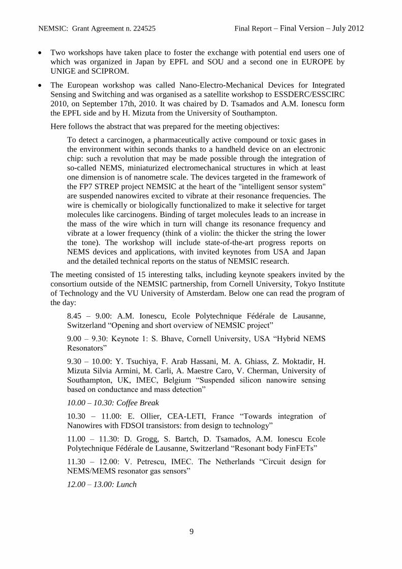
The meeting consisted of 15 interesting talks, including keynote speakers invited by the
consortium outside of the NEMSIC partnership, from Cornell University, Tokyo Institute
of Technology and the VU University of Amsterdam. Below one can read the program of
the day:
8.45 – 9.00: A.M. Ionescu, Ecole Polytechnique Fédérale de Lausanne,
Switzerland “Opening and short overview of NEMSIC project”
9.00 – 9.30: Keynote 1: S. Bhave, Cornell University, USA “Hybrid NEMS
Resonators”
9.30 – 10.00: Y. Tsuchiya, F. Arab Hassani, M. A. Ghiass, Z. Moktadir, H.
Mizuta Silvia Armini, M. Carli, A. Maestre Caro, V. Cherman, University of
Southampton, UK, IMEC, Belgium “Suspended silicon nanowire sensing
based on conductance and mass detection”
10.00 – 10.30: Coffee Break
10.30 – 11.00: E. Ollier, CEA-LETI, France “Towards integration of
Nanowires with FDSOI transistors: from design to technology”
11.00 – 11.30: D. Grogg, S. Bartch, D. Tsamados, A.M. Ionescu Ecole
Polytechnique Fédérale de Lausanne, Switzerland “Resonant body FinFETs”
11.30 – 12.00: V. Petrescu, IMEC. The Netherlands “Circuit design for
NEMS/MEMS resonator gas sensors”
12.00 – 13.00: Lunch
NEMSIC: Grant Agreement n. 224525 Final Report – Final Version – July 2012
10
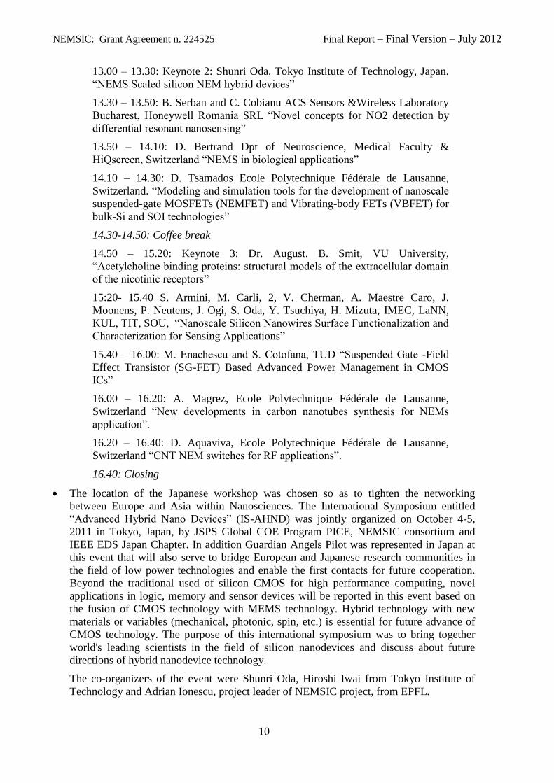
13.00 – 13.30: Keynote 2: Shunri Oda, Tokyo Institute of Technology, Japan.
“NEMS Scaled silicon NEM hybrid devices”
13.30 – 13.50: B. Serban and C. Cobianu ACS Sensors &Wireless Laboratory
Bucharest, Honeywell Romania SRL “Novel concepts for NO2 detection by
differential resonant nanosensing”
13.50 – 14.10: D. Bertrand Dpt of Neuroscience, Medical Faculty &
HiQscreen, Switzerland “NEMS in biological applications”
14.10 – 14.30: D. Tsamados Ecole Polytechnique Fédérale de Lausanne,
Switzerland. “Modeling and simulation tools for the development of nanoscale
suspended-gate MOSFETs (NEMFET) and Vibrating-body FETs (VBFET) for
bulk-Si and SOI technologies”
14.30-14.50: Coffee break
14.50 – 15.20: Keynote 3: Dr. August. B. Smit, VU University,
“Acetylcholine binding proteins: structural models of the extracellular domain
of the nicotinic receptors”
15:20- 15.40 S. Armini, M. Carli, 2, V. Cherman, A. Maestre Caro, J.
Moonens, P. Neutens, J. Ogi, S. Oda, Y. Tsuchiya, H. Mizuta, IMEC, LaNN,
KUL, TIT, SOU, “Nanoscale Silicon Nanowires Surface Functionalization and
Characterization for Sensing Applications”
15.40 – 16.00: M. Enachescu and S. Cotofana, TUD “Suspended Gate -Field
Effect Transistor (SG-FET) Based Advanced Power Management in CMOS
ICs”
16.00 – 16.20: A. Magrez, Ecole Polytechnique Fédérale de Lausanne,
Switzerland “New developments in carbon nanotubes synthesis for NEMs
application”.
16.20 – 16.40: D. Aquaviva, Ecole Polytechnique Fédérale de Lausanne,
Switzerland “CNT NEM switches for RF applications”.
16.40: Closing
The location of the Japanese workshop was chosen so as to tighten the networking
between Europe and Asia within Nanosciences. The International Symposium entitled
“Advanced Hybrid Nano Devices” (IS-AHND) was jointly organized on October 4-5,
2011 in Tokyo, Japan, by JSPS Global COE Program PICE, NEMSIC consortium and
IEEE EDS Japan Chapter. In addition Guardian Angels Pilot was represented in Japan at
this event that will also serve to bridge European and Japanese research communities in
the field of low power technologies and enable the first contacts for future cooperation.
Beyond the traditional used of silicon CMOS for high performance computing, novel
applications in logic, memory and sensor devices will be reported in this event based on
the fusion of CMOS technology with MEMS technology. Hybrid technology with new
materials or variables (mechanical, photonic, spin, etc.) is essential for future advance of
CMOS technology. The purpose of this international symposium was to bring together
world's leading scientists in the field of silicon nanodevices and discuss about future
directions of hybrid nanodevice technology.
The co-organizers of the event were Shunri Oda, Hiroshi Iwai from Tokyo Institute of
Technology and Adrian Ionescu, project leader of NEMSIC project, from EPFL.
NEMSIC: Grant Agreement n. 224525 Final Report – Final Version – July 2012
11
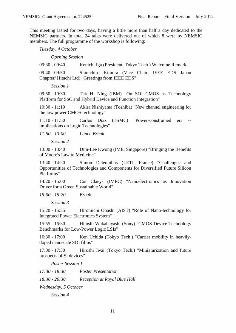
This meeting lasted for two days, having a little more than half a day dedicated to the
NEMSIC partners. In total 24 talks were delivered out of which 8 were by NEMSIC
members. The full programme of the workshop is following:
Tuesday, 4 October
Opening Session
09:30 - 09:40 Kenichi Iga (President, Tokyo Tech.) Welcome Remark
09:40 - 09:50 Shinichiro Kimura (Vice Chair, IEEE EDS Japan
Chapter/ Hitachi Ltd) "Greetings from IEEE EDS"
Session 1
09:50 - 10:30 Tak H. Ning (IBM) "On SOI CMOS as Technology
Platform for SoC and Hybrid Device and Function Integration"
10:30 - 11:10 Akira Nishiyama (Toshiba) "New channel engineering for
the low power CMOS technology"
11:10 - 11:50 Carlos Diaz (TSMC) "Power-constrained era --
implications on Logic Technologies"
11:50 - 13:00 Lunch Break
Session 2
13:00 - 13:40 Dim-Lee Kwong (IME, Singapore) "Bringing the Benefits
of Moore's Law to Medicine"
13:40 - 14:20 Simon Deleonibus (LETI, France) "Challenges and
Opportunities of Technologies and Components for Diversified Future Silicon
Platforms"
14:20 - 15:00 Cor Claeys (IMEC) "Nanoelectronics as Innovation
Driver for a Green Sustainable World"
15:00 - 15:20 Break
Session 3
15:20 - 15:55 Hiromichi Ohashi (AIST) "Role of Nano-technology for
Integrated Power Electronics System"
15:55 - 16:30 Hitoshi Wakabayashi (Sony) "CMOS-Device Technology
Benchmarks for Low-Power Logic LSIs"
16:30 - 17:00 Ken Uchida (Tokyo Tech.) "Carrier mobility in heavily-
doped nanoscale SOI films"
17:00 - 17:30 Hiroshi Iwai (Tokyo Tech.) "Miniaturization and future
prospects of Si devices"
Poster Session 1
17:30 - 18:30 Poster Presentation
18:30 - 20:30 Reception at Royal Blue Hall
Wednesday, 5 October
Session 4
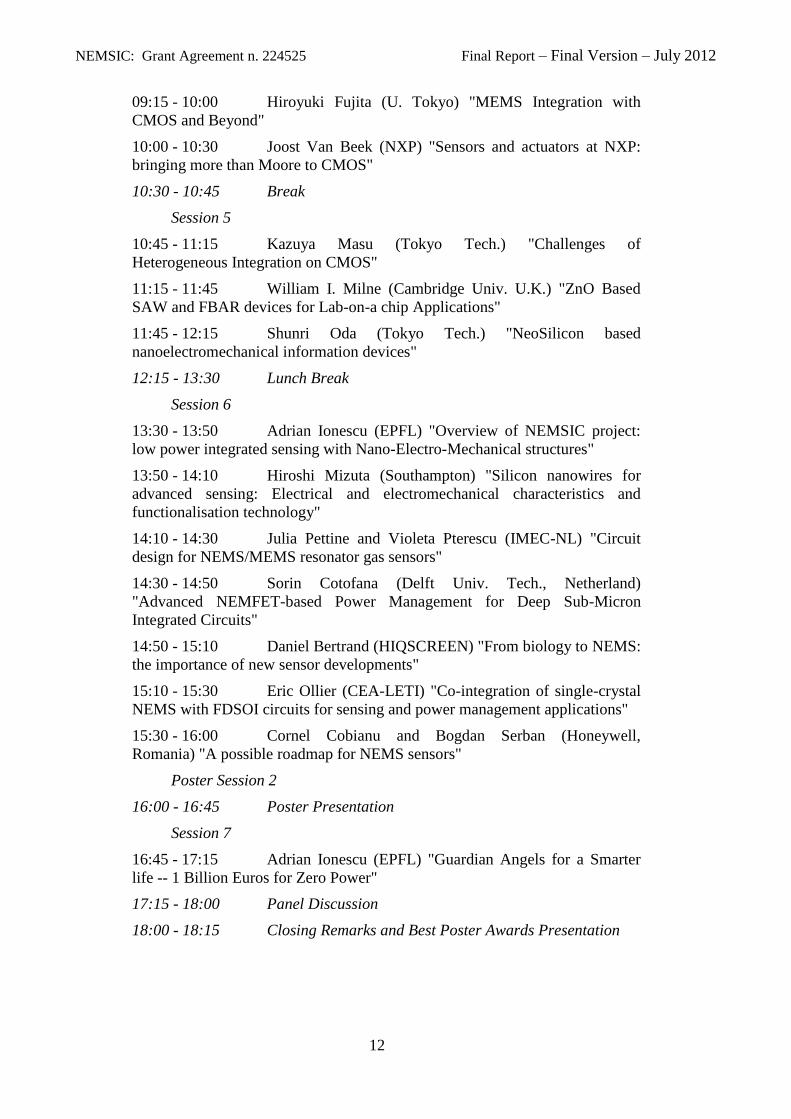
NEMSIC: Grant Agreement n. 224525 Final Report – Final Version – July 2012
12
09:15 - 10:00 Hiroyuki Fujita (U. Tokyo) "MEMS Integration with
CMOS and Beyond"
10:00 - 10:30 Joost Van Beek (NXP) "Sensors and actuators at NXP:
bringing more than Moore to CMOS"
10:30 - 10:45 Break
Session 5
10:45 - 11:15 Kazuya Masu (Tokyo Tech.) "Challenges of
Heterogeneous Integration on CMOS"
11:15 - 11:45 William I. Milne (Cambridge Univ. U.K.) "ZnO Based
SAW and FBAR devices for Lab-on-a chip Applications"
11:45 - 12:15 Shunri Oda (Tokyo Tech.) "NeoSilicon based
nanoelectromechanical information devices"
12:15 - 13:30 Lunch Break
Session 6
13:30 - 13:50 Adrian Ionescu (EPFL) "Overview of NEMSIC project:
low power integrated sensing with Nano-Electro-Mechanical structures"
13:50 - 14:10 Hiroshi Mizuta (Southampton) "Silicon nanowires for
advanced sensing: Electrical and electromechanical characteristics and
functionalisation technology"
14:10 - 14:30 Julia Pettine and Violeta Pterescu (IMEC-NL) "Circuit
design for NEMS/MEMS resonator gas sensors"
14:30 - 14:50 Sorin Cotofana (Delft Univ. Tech., Netherland)
"Advanced NEMFET-based Power Management for Deep Sub-Micron
Integrated Circuits"
14:50 - 15:10 Daniel Bertrand (HIQSCREEN) "From biology to NEMS:
the importance of new sensor developments"
15:10 - 15:30 Eric Ollier (CEA-LETI) "Co-integration of single-crystal
NEMS with FDSOI circuits for sensing and power management applications"
15:30 - 16:00 Cornel Cobianu and Bogdan Serban (Honeywell,
Romania) "A possible roadmap for NEMS sensors"
Poster Session 2
16:00 - 16:45 Poster Presentation
Session 7
16:45 - 17:15 Adrian Ionescu (EPFL) "Guardian Angels for a Smarter
life -- 1 Billion Euros for Zero Power"
17:15 - 18:00 Panel Discussion
18:00 - 18:15 Closing Remarks and Best Poster Awards Presentation
NEMSIC: Grant Agreement n. 224525 Final Report – Final Version – July 2012
13
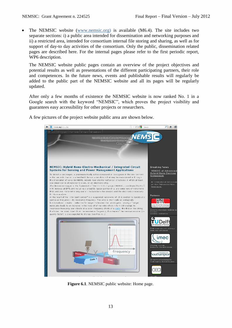
The NEMSIC website (www.nemsic.org) is available (M6.4). The site includes two
separate sections: i) a public area intended for dissemination and networking purposes and
ii) a restricted area, intended for consortium internal file storing and sharing, as well as for
support of day-to day activities of the consortium. Only the public, dissemination related
pages are described here. For the internal pages please refer to the first periodic report,
WP6 description.
The NEMSIC website public pages contain an overview of the project objectives and
potential results as well as presentations of the different participating partners, their role
and competences. In the future news, events and publishable results will regularly be
added to the public part of the NEMSIC website and all its pages will be regularly
updated.
After only a few months of existence the NEMSIC website is now ranked No. 1 in a
Google search with the keyword “NEMSIC”, which proves the project visibility and
guarantees easy accessibility for other projects or researchers.
A few pictures of the project website public area are shown below.
Figure 6.1. NEMSIC public website: Home page.
NEMSIC: Grant Agreement n. 224525 Final Report – Final Version – July 2012
14
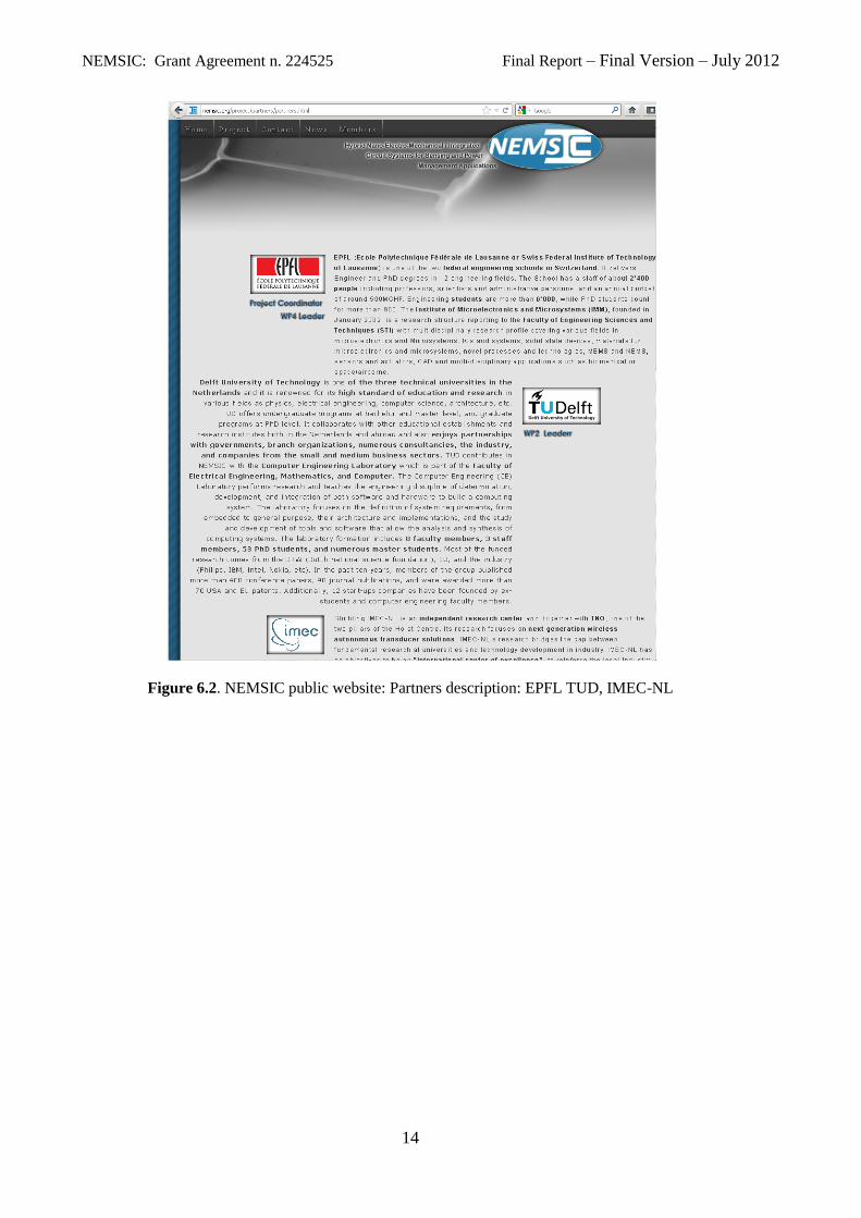
Figure 6.2. NEMSIC public website: Partners description: EPFL TUD, IMEC-NL
NEMSIC: Grant Agreement n. 224525 Final Report – Final Version – July 2012
15
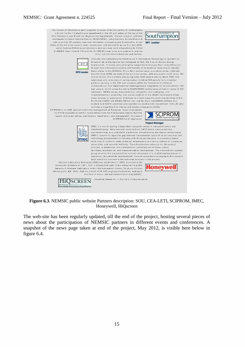
Figure 6.3. NEMSIC public website Partners description: SOU, CEA-LETI, SCIPROM, IMEC,
Honeywell, HiQscreen
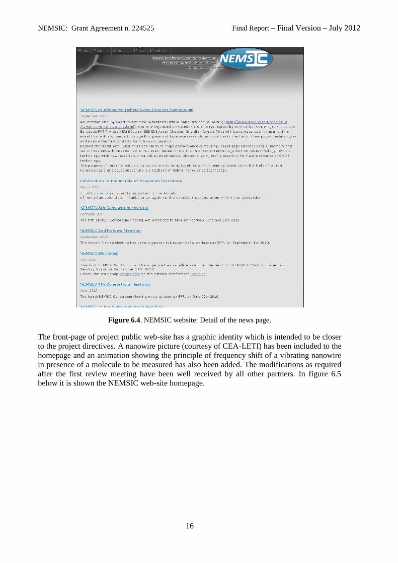
The web-site has been regularly updated, till the end of the project, hosting several pieces of
news about the participation of NEMSIC partners in different events and conferences. A
snapshot of the news page taken at end of the project, May 2012, is visible here below in
figure 6.4.
NEMSIC: Grant Agreement n. 224525 Final Report – Final Version – July 2012
16
Figure 6.4. NEMSIC website: Detail of the news page.
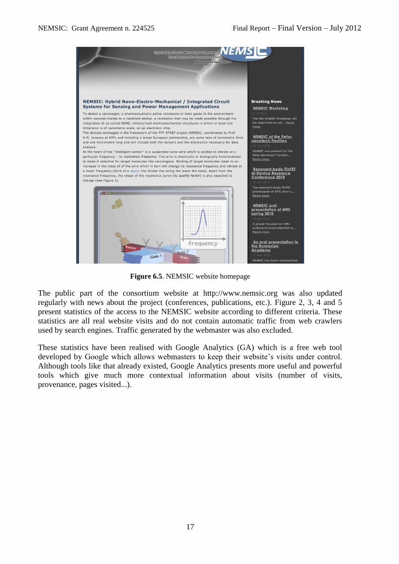
The front-page of project public web-site has a graphic identity which is intended to be closer
to the project directives. A nanowire picture (courtesy of CEA-LETI) has been included to the
homepage and an animation showing the principle of frequency shift of a vibrating nanowire
in presence of a molecule to be measured has also been added. The modifications as required
after the first review meeting have been well received by all other partners. In figure 6.5
below it is shown the NEMSIC web-site homepage.
NEMSIC: Grant Agreement n. 224525 Final Report – Final Version – July 2012
17
Figure 6.5. NEMSIC website homepage
The public part of the consortium website at http://www.nemsic.org was also updated
regularly with news about the project (conferences, publications, etc.). Figure 2, 3, 4 and 5
present statistics of the access to the NEMSIC website according to different criteria. These
statistics are all real website visits and do not contain automatic traffic from web crawlers
used by search engines. Traffic generated by the webmaster was also excluded.
These statistics have been realised with Google Analytics (GA) which is a free web tool
developed by Google which allows webmasters to keep their website’s visits under control.
Although tools like that already existed, Google Analytics presents more useful and powerful
tools which give much more contextual information about visits (number of visits,
provenance, pages visited...).
NEMSIC: Grant Agreement n. 224525 Final Report – Final Version – July 2012
18
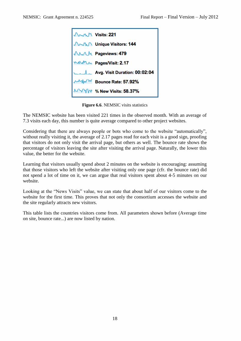
Figure 6.6. NEMSIC visits statistics
The NEMSIC website has been visited 221 times in the observed month. With an average of
7.3 visits each day, this number is quite average compared to other project websites.
Considering that there are always people or bots who come to the website “automatically”,
without really visiting it, the average of 2.17 pages read for each visit is a good sign, proofing
that visitors do not only visit the arrival page, but others as well. The bounce rate shows the
percentage of visitors leaving the site after visiting the arrival page. Naturally, the lower this
value, the better for the website.
Learning that visitors usually spend about 2 minutes on the website is encouraging: assuming
that those visitors who left the website after visiting only one page (cfr. the bounce rate) did
not spend a lot of time on it, we can argue that real visitors spent about 4-5 minutes on our
website.
Looking at the “News Visits” value, we can state that about half of our visitors come to the
website for the first time. This proves that not only the consortium accesses the website and
the site regularly attracts new visitors.
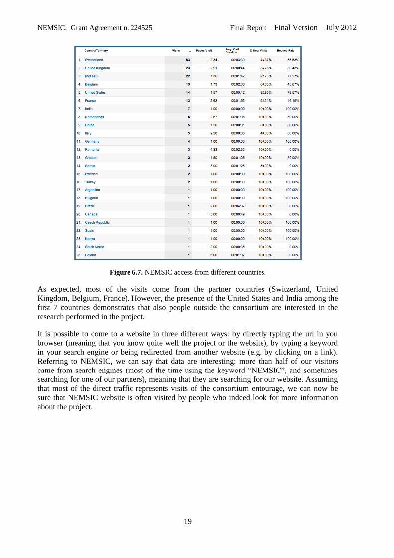
This table lists the countries visitors come from. All parameters shown before (Average time
on site, bounce rate...) are now listed by nation.
NEMSIC: Grant Agreement n. 224525 Final Report – Final Version – July 2012
19
Figure 6.7. NEMSIC access from different countries.
As expected, most of the visits come from the partner countries (Switzerland, United
Kingdom, Belgium, France). However, the presence of the United States and India among the
first 7 countries demonstrates that also people outside the consortium are interested in the
research performed in the project.
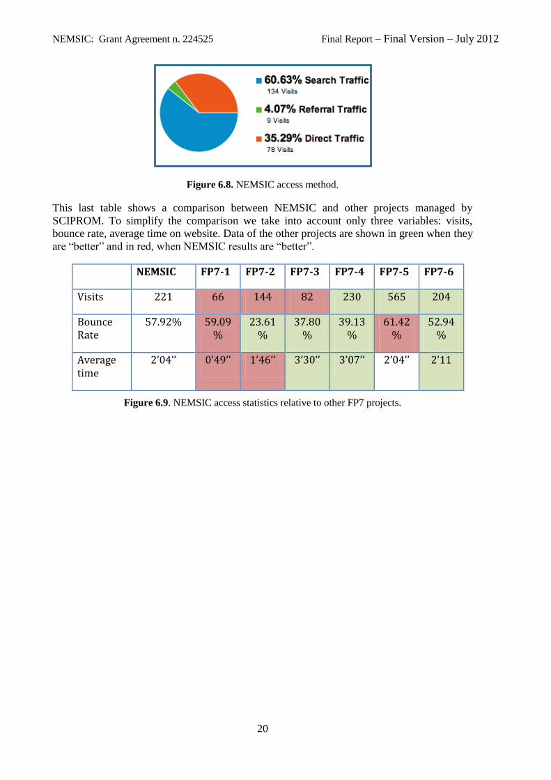
It is possible to come to a website in three different ways: by directly typing the url in you
browser (meaning that you know quite well the project or the website), by typing a keyword
in your search engine or being redirected from another website (e.g. by clicking on a link).
Referring to NEMSIC, we can say that data are interesting: more than half of our visitors
came from search engines (most of the time using the keyword “NEMSIC”, and sometimes
searching for one of our partners), meaning that they are searching for our website. Assuming
that most of the direct traffic represents visits of the consortium entourage, we can now be
sure that NEMSIC website is often visited by people who indeed look for more information
about the project.
NEMSIC: Grant Agreement n. 224525 Final Report – Final Version – July 2012
20
Figure 6.8. NEMSIC access method.
This last table shows a comparison between NEMSIC and other projects managed by
SCIPROM. To simplify the comparison we take into account only three variables: visits,
bounce rate, average time on website. Data of the other projects are shown in green when they
are “better” and in red, when NEMSIC results are “better”.
NEMSIC FP7-1 FP7-2 FP7-3 FP7-4 FP7-5 FP7-6
Visits 221 66 144 82 230 565 204
Bounce Rate
57.92% 59.09%
23.61%
37.80%
39.13%
61.42%
52.94%
Average time
2’04’’ 0’49’’ 1’46’’ 3’30’’ 3’07’’ 2’04’’ 2’11
Figure 6.9. NEMSIC access statistics relative to other FP7 projects.
NEMSIC: Grant Agreement n. 224525 Final Report – Final Version – July 2012
21
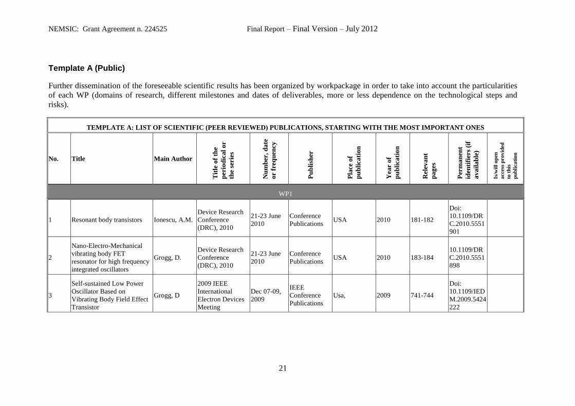
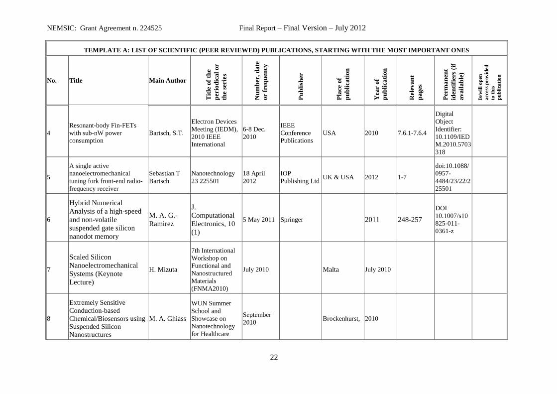
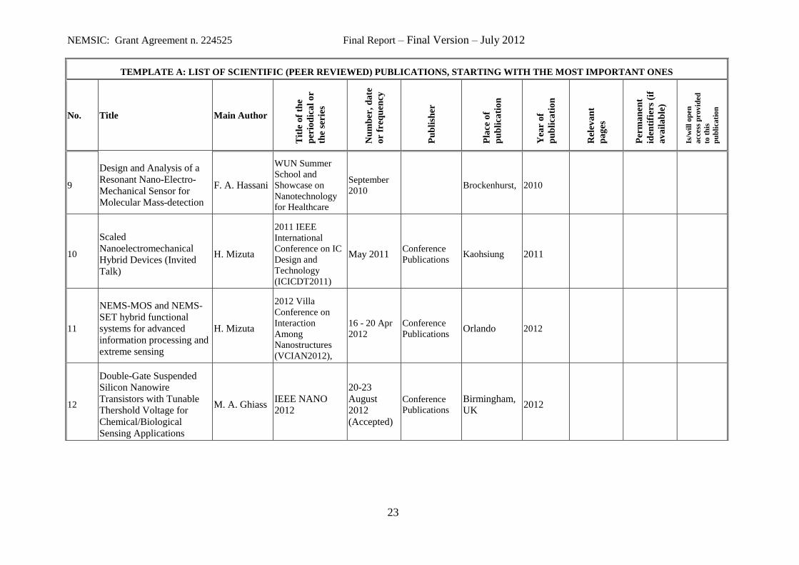
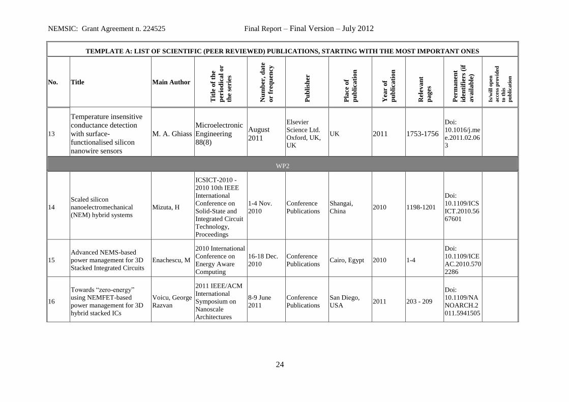
Template A (Public)
Further dissemination of the foreseeable scientific results has been organized by workpackage in order to take into account the particularities
of each WP (domains of research, different milestones and dates of deliverables, more or less dependence on the technological steps and
risks).
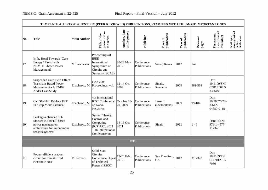
TEMPLATE A: LIST OF SCIENTIFIC (PEER REVIEWED) PUBLICATIONS, STARTING WITH THE MOST IMPORTANT ONES
No. Title Main Author
Tit
le o
f th
e
per
iod
ica
l o
r
the
serie
s
Nu
mb
er,
da
te
or
freq
uen
cy
Pu
bli
sher
Pla
ce o
f
pu
bli
cati
on
Yea
r o
f
pu
bli
cati
on
Rel
ev
an
t
pa
ges
Per
ma
nen
t
iden
tifi
ers
(if
av
ail
ab
le)
Is/w
ill
op
en
acce
ss p
rov
ided
to t
his
pu
bli
cati
on
WP1
1 Resonant body transistors Ionescu, A.M.
Device Research
Conference
(DRC), 2010
21-23 June
2010
Conference
Publications USA 2010 181-182
Doi:
10.1109/DR
C.2010.5551
901
2
Nano-Electro-Mechanical
vibrating body FET
resonator for high frequency
integrated oscillators
Grogg, D.
Device Research
Conference
(DRC), 2010
21-23 June
2010
Conference
Publications USA 2010 183-184
10.1109/DR
C.2010.5551
898
3
Self-sustained Low Power
Oscillator Based on
Vibrating Body Field Effect
Transistor
Grogg, D
2009 IEEE
International
Electron Devices
Meeting
Dec 07-09,
2009
IEEE
Conference
Publications
Usa, 2009 741-744
Doi:
10.1109/IED
M.2009.5424
222
NEMSIC: Grant Agreement n. 224525 Final Report – Final Version – July 2012
22
TEMPLATE A: LIST OF SCIENTIFIC (PEER REVIEWED) PUBLICATIONS, STARTING WITH THE MOST IMPORTANT ONES
No. Title Main Author
Tit
le o
f th
e
per
iod
ica
l o
r
the
serie
s
Nu
mb
er,
da
te
or
freq
uen
cy
Pu
bli
sher
Pla
ce o
f
pu
bli
cati
on
Yea
r o
f
pu
bli
cati
on
Rel
ev
an
t
pa
ges
Per
ma
nen
t
iden
tifi
ers
(if
av
ail
ab
le)
Is/w
ill
op
en
acce
ss p
rov
ided
to t
his
pu
bli
cati
on
4
Resonant-body Fin-FETs
with sub-nW power
consumption
Bartsch, S.T.
Electron Devices
Meeting (IEDM),
2010 IEEE
International
6-8 Dec.
2010
IEEE
Conference
Publications
USA 2010 7.6.1-7.6.4
Digital
Object
Identifier:
10.1109/IED
M.2010.5703
318
5
A single active
nanoelectromechanical
tuning fork front-end radio-
frequency receiver
Sebastian T
Bartsch
Nanotechnology
23 225501
18 April
2012
IOP
Publishing Ltd UK & USA 2012 1-7
doi:10.1088/
0957-
4484/23/22/2
25501
6
Hybrid Numerical
Analysis of a high-speed
and non-volatile
suspended gate silicon
nanodot memory
M. A. G.-
Ramirez
J.
Computational
Electronics, 10
(1)
5 May 2011 Springer 2011 248-257
DOI
10.1007/s10
825-011-
0361-z
7
Scaled Silicon
Nanoelectromechanical
Systems (Keynote
Lecture)
H. Mizuta
7th International
Workshop on
Functional and
Nanostructured
Materials
(FNMA2010)
July 2010 Malta July 2010
8
Extremely Sensitive
Conduction-based
Chemical/Biosensors using Suspended Silicon
Nanostructures
M. A. Ghiass
WUN Summer
School and
Showcase on
Nanotechnology
for Healthcare
September
2010 Brockenhurst, 2010
NEMSIC: Grant Agreement n. 224525 Final Report – Final Version – July 2012
23
TEMPLATE A: LIST OF SCIENTIFIC (PEER REVIEWED) PUBLICATIONS, STARTING WITH THE MOST IMPORTANT ONES
No. Title Main Author
Tit
le o
f th
e
per
iod
ica
l o
r
the
serie
s
Nu
mb
er,
da
te
or
freq
uen
cy
Pu
bli
sher
Pla
ce o
f
pu
bli
cati
on
Yea
r o
f
pu
bli
cati
on
Rel
ev
an
t
pa
ges
Per
ma
nen
t
iden
tifi
ers
(if
av
ail
ab
le)
Is/w
ill
op
en
acce
ss p
rov
ided
to t
his
pu
bli
cati
on
9
Design and Analysis of a
Resonant Nano-Electro-
Mechanical Sensor for
Molecular Mass-detection
F. A. Hassani
WUN Summer
School and
Showcase on
Nanotechnology
for Healthcare
September
2010 Brockenhurst, 2010
10
Scaled
Nanoelectromechanical
Hybrid Devices (Invited
Talk)
H. Mizuta
2011 IEEE
International
Conference on IC
Design and
Technology
(ICICDT2011)
May 2011 Conference
Publications Kaohsiung 2011
11
NEMS-MOS and NEMS-
SET hybrid functional
systems for advanced
information processing and
extreme sensing
H. Mizuta
2012 Villa
Conference on
Interaction
Among
Nanostructures
(VCIAN2012),
16 - 20 Apr
2012
Conference
Publications Orlando 2012
12
Double-Gate Suspended
Silicon Nanowire
Transistors with Tunable
Thershold Voltage for
Chemical/Biological
Sensing Applications
M. A. Ghiass IEEE NANO
2012
20-23
August
2012
(Accepted)
Conference
Publications
Birmingham,
UK 2012
NEMSIC: Grant Agreement n. 224525 Final Report – Final Version – July 2012
24
TEMPLATE A: LIST OF SCIENTIFIC (PEER REVIEWED) PUBLICATIONS, STARTING WITH THE MOST IMPORTANT ONES
No. Title Main Author
Tit
le o
f th
e
per
iod
ica
l o
r
the
serie
s
Nu
mb
er,
da
te
or
freq
uen
cy
Pu
bli
sher
Pla
ce o
f
pu
bli
cati
on
Yea
r o
f
pu
bli
cati
on
Rel
ev
an
t
pa
ges
Per
ma
nen
t
iden
tifi
ers
(if
av
ail
ab
le)
Is/w
ill
op
en
acce
ss p
rov
ided
to t
his
pu
bli
cati
on
13
Temperature insensitive
conductance detection
with surface-
functionalised silicon
nanowire sensors
M. A. Ghiass
Microelectronic
Engineering
88(8)
August
2011
Elsevier
Science Ltd.
Oxford, UK,
UK
UK 2011 1753-1756
Doi:
10.1016/j.me
e.2011.02.06
3
WP2
14
Scaled silicon
nanoelectromechanical
(NEM) hybrid systems
Mizuta, H
ICSICT-2010 -
2010 10th IEEE
International
Conference on
Solid-State and
Integrated Circuit
Technology,
Proceedings
1-4 Nov.
2010
Conference
Publications
Shangai,
China 2010 1198-1201
Doi:
10.1109/ICS
ICT.2010.56
67601
15
Advanced NEMS-based
power management for 3D
Stacked Integrated Circuits
Enachescu, M
2010 International
Conference on
Energy Aware
Computing
16-18 Dec.
2010
Conference
Publications Cairo, Egypt 2010 1-4
Doi:
10.1109/ICE
AC.2010.570
2286
16
Towards “zero-energy”
using NEMFET-based
power management for 3D
hybrid stacked ICs
Voicu, George
Razvan
2011 IEEE/ACM
International
Symposium on
Nanoscale
Architectures
8-9 June
2011
Conference
Publications
San Diego,
USA 2011 203 - 209
Doi:
10.1109/NA
NOARCH.2
011.5941505
NEMSIC: Grant Agreement n. 224525 Final Report – Final Version – July 2012
25
TEMPLATE A: LIST OF SCIENTIFIC (PEER REVIEWED) PUBLICATIONS, STARTING WITH THE MOST IMPORTANT ONES
No. Title Main Author
Tit
le o
f th
e
per
iod
ica
l o
r
the
serie
s
Nu
mb
er,
da
te
or
freq
uen
cy
Pu
bli
sher
Pla
ce o
f
pu
bli
cati
on
Yea
r o
f
pu
bli
cati
on
Rel
ev
an
t
pa
ges
Per
ma
nen
t
iden
tifi
ers
(if
av
ail
ab
le)
Is/w
ill
op
en
acce
ss p
rov
ided
to t
his
pu
bli
cati
on
17
Is the Road Towards “Zero-
Energy” Paved with
NEMFET-based Power
Management?
M Enachescu
Proceedings of
IEEE
International
Symposium on
Circuits and
Systems (ISCAS)
20-23 May
2012
Conference
Publications Seoul, Korea 2012 1-4
18
Suspended Gate Field Effect
Transistor Based Power
Management - A 32-Bit
Adder Case Study
Enachescu, M
CAS 2009
Proceedings, vol.
2.
12-14 Oct.
2009
Conference
Publications
Sinaia,
Romania 2009 561-564
Doi:
10.1109/SMI
CND.2009.5
336649
19 Can SG-FET Replace FET
In Sleep Mode Circuits? Enachescu, M
4th International
ICST Conference
on Nano-
Networks
October 18-
20, 2009
Conference
Publications
Luzern
(Switzerland) 2009 99-104
Doi:
10.1007/978-
3-642-
04850-0_15
20
Leakage-enhanced 3D-
Stacked NEMFET-based
power management
architecture for autonomous
sensors systems
Enachescu, M.
System Theory,
Control, and
Computing
(ICSTCC), 2011
15th International
Conference on
14-16 Oct.
2011
Conference
Publications Sinaia 2011 1 - 6
Print ISBN:
978-1-4577-
1173-2
WP3
21
Power-efficient readout
circuit for miniaturized
electronic nose
V. Petrescu
Solid-State
Circuits
Conference Digest
of Technical
Papers (ISSCC)
19-23 Feb.
2012
Conference
Publications
San Francisco,
CA 2012 318-320
Doi:
10.1109/ISS
CC.2012.617
7030
NEMSIC: Grant Agreement n. 224525 Final Report – Final Version – July 2012
26
TEMPLATE A: LIST OF SCIENTIFIC (PEER REVIEWED) PUBLICATIONS, STARTING WITH THE MOST IMPORTANT ONES
No. Title Main Author
Tit
le o
f th
e
per
iod
ica
l o
r
the
serie
s
Nu
mb
er,
da
te
or
freq
uen
cy
Pu
bli
sher
Pla
ce o
f
pu
bli
cati
on
Yea
r o
f
pu
bli
cati
on
Rel
ev
an
t
pa
ges
Per
ma
nen
t
iden
tifi
ers
(if
av
ail
ab
le)
Is/w
ill
op
en
acce
ss p
rov
ided
to t
his
pu
bli
cati
on
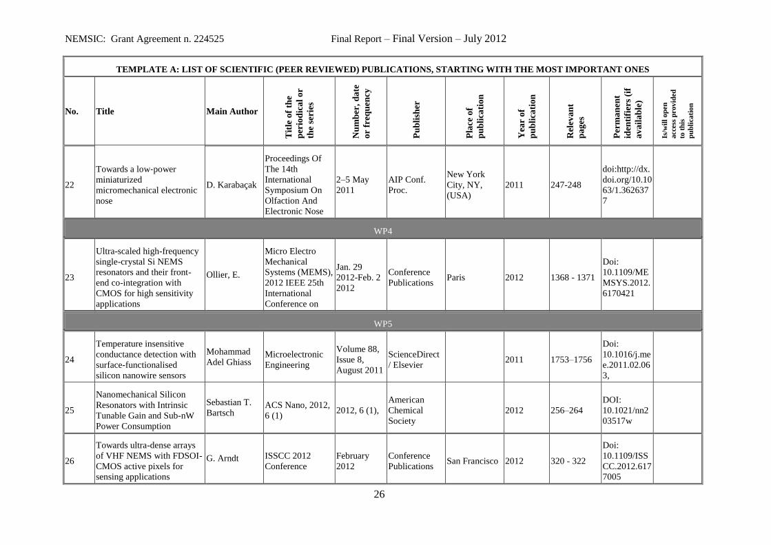
22
Towards a low‐power
miniaturized
micromechanical electronic
nose
D. Karabaçak
Proceedings Of
The 14th
International
Symposium On
Olfaction And
Electronic Nose
2–5 May
2011
AIP Conf.
Proc.
New York
City, NY,
(USA)
2011 247-248
doi:http://dx.
doi.org/10.10
63/1.362637
7
WP4
23
Ultra-scaled high-frequency
single-crystal Si NEMS
resonators and their front-
end co-integration with
CMOS for high sensitivity
applications
Ollier, E.
Micro Electro
Mechanical
Systems (MEMS),
2012 IEEE 25th
International
Conference on
Jan. 29
2012-Feb. 2
2012
Conference
Publications Paris 2012 1368 - 1371
Doi:
10.1109/ME
MSYS.2012.
6170421
WP5
24
Temperature insensitive
conductance detection with
surface-functionalised
silicon nanowire sensors
Mohammad
Adel Ghiass Microelectronic
Engineering
Volume 88,
Issue 8,
August 2011
ScienceDirect
/ Elsevier 2011 1753–1756
Doi:
10.1016/j.me
e.2011.02.06
3,
25
Nanomechanical Silicon
Resonators with Intrinsic
Tunable Gain and Sub-nW
Power Consumption
Sebastian T.
Bartsch ACS Nano, 2012,
6 (1) 2012, 6 (1),
American
Chemical
Society
2012 256–264
DOI:
10.1021/nn2
03517w
26
Towards ultra-dense arrays
of VHF NEMS with FDSOI-
CMOS active pixels for
sensing applications
G. Arndt ISSCC 2012
Conference
February
2012
Conference
Publications San Francisco 2012 320 - 322
Doi:
10.1109/ISS
CC.2012.617
7005
NEMSIC: Grant Agreement n. 224525 Final Report – Final Version – July 2012
27
TEMPLATE A: LIST OF SCIENTIFIC (PEER REVIEWED) PUBLICATIONS, STARTING WITH THE MOST IMPORTANT ONES
No. Title Main Author
Tit
le o
f th
e
per
iod
ica
l o
r
the
serie
s
Nu
mb
er,
da
te
or
freq
uen
cy
Pu
bli
sher
Pla
ce o
f
pu
bli
cati
on
Yea
r o
f
pu
bli
cati
on
Rel
ev
an
t
pa
ges
Per
ma
nen
t
iden
tifi
ers
(if
av
ail
ab
le)
Is/w
ill
op
en
acce
ss p
rov
ided
to t
his
pu
bli
cati
on
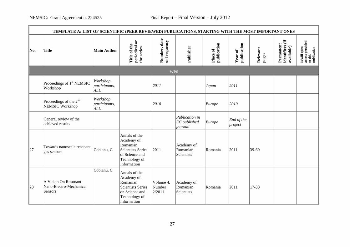
WP6
Proceedings of 1
st NEMSIC
Workshop
Workshop
participants,
ALL
2011 Japan 2011
Proceedings of the 2
nd
NEMSIC Workshop
Workshop
participants,
ALL
2010 Europe 2010
General review of the
achieved results
Publication in
EC published
jourmal
Europe End of the
project
27 Towards nanoscale resonant
gas sensors Cobianu, C
Annals of the
Academy of
Romanian
Scientists Series
of Science and
Technology of
Information
2011
Academy of
Romanian
Scientists
Romania 2011 39-60
28
A Vision On Resonant
Nano-Electro-Mechanical
Sensors
Cobianu, C Annals of the
Academy of
Romanian
Scientists Series
on Science and
Technology of
Information
Volume 4,
Number
2/2011
Academy of
Romanian
Scientists
Romania 2011 17-38
NEMSIC: Grant Agreement n. 224525 Final Report – Final Version – July 2012
28
TEMPLATE A: LIST OF SCIENTIFIC (PEER REVIEWED) PUBLICATIONS, STARTING WITH THE MOST IMPORTANT ONES
No. Title Main Author
Tit
le o
f th
e
per
iod
ica
l o
r
the
serie
s
Nu
mb
er,
da
te
or
freq
uen
cy
Pu
bli
sher
Pla
ce o
f
pu
bli
cati
on
Yea
r o
f
pu
bli
cati
on
Rel
ev
an
t
pa
ges
Per
ma
nen
t
iden
tifi
ers
(if
av
ail
ab
le)
Is/w
ill
op
en
acce
ss p
rov
ided
to t
his
pu
bli
cati
on
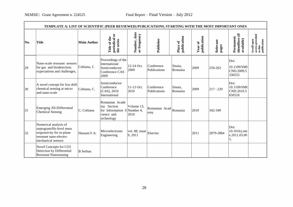
29
Nano-scale resonant sensors
for gas and biodetection:
expectations and challenges,
Cobianu, C
Proceedings of the
International
Semiconductor
Conference CAS
2009
12-14 Oct.
2009
Conference
Publications
Sinaia,
Romania 2009 259-262
Doi:
10.1109/SMI
CND.2009.5
336553
30
A novel concept for low drift
chemical sensing at micro
and nano-scale Cobianu, C.
Semiconductor
Conference
(CAS), 2010
International
11-13 Oct.
2010
Conference
Publications
Sinaia,
Romania 2009 217 - 220
Doi:
10.1109/SMI
CND.2010.5
650518
31 Emerging All-Differential
Chemical Sensing C. Cobianu
Romanian Acade
my Section
for Information S
cience and
technology
Volume 13,
Number 4,
2010
Romanian Acad
emy Romania 2010 342-349
32
Numerical analysis of
zeptogram/Hz-level mass
responsivity for in-plane
resonant nano-electro-
mechanical sensors
Hassani F.A. Microelectronic
Engineering
vol. 88, issue
9, 2011 Elsevier 2011 2879-2884
Doi:
10.1016/j.me
e.2011.03.00
5,
Novel Concepts for CO2
Detection by Differential
Resonant Nanosensing B Serban
NEMSIC: Grant Agreement n. 224525 Final Report – Final Version – July 2012
29
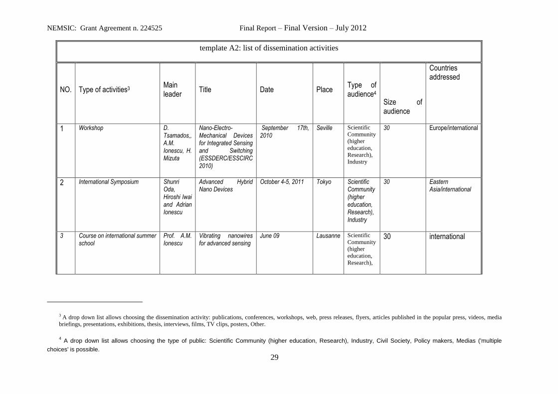
template A2: list of dissemination activities
NO. Type of activities3 Main leader
Title Date Place Type of audience4
Size of audience
Countries addressed
1 Workshop D. Tsamados,, A.M. Ionescu, H. Mizuta
Nano-Electro-Mechanical Devices for Integrated Sensing and Switching (ESSDERC/ESSCIRC 2010)
September 17th, 2010
Seville Scientific
Community
(higher
education,
Research),
Industry
30 Europe/international
2 International Symposium Shunri Oda, Hiroshi Iwai and Adrian Ionescu
Advanced Hybrid Nano Devices
October 4-5, 2011 Tokyo Scientific Community (higher education, Research), Industry
30 Eastern Asia/international
3 Course on international summer school
Prof. A.M. Ionescu
Vibrating nanowires for advanced sensing
June 09 Lausanne Scientific
Community
(higher
education,
Research),
30 international
3 A drop down list allows choosing the dissemination activity: publications, conferences, workshops, web, press releases, flyers, articles published in the popular press, videos, media
briefings, presentations, exhibitions, thesis, interviews, films, TV clips, posters, Other.
4 A drop down list allows choosing the type of public: Scientific Community (higher education, Research), Industry, Civil Society, Policy makers, Medias ('multiple
choices' is possible.
NEMSIC: Grant Agreement n. 224525 Final Report – Final Version – July 2012
30
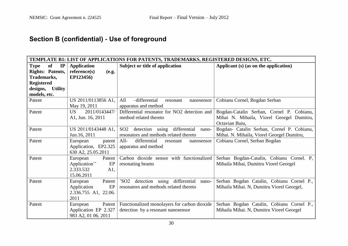
Section B (confidential) - Use of foreground
TEMPLATE B1: LIST OF APPLICATIONS FOR PATENTS, TRADEMARKS, REGISTERED DESIGNS, ETC.
Type of IP
Rights: Patents,
Trademarks,
Registered
designs, Utility
models, etc.
Application
reference(s) (e.g.
EP123456)
Subject or title of application Applicant (s) (as on the application)
Patent US 2011/0113856 A1,
May 19, 2011
All –differential resonant nanosensor
apparatus and method
Cobianu Cornel, Bogdan Serban
Patent US 2011/0143447/
A1, Jun. 16, 2011
Differential resonator for NO2 detection and
method related thereto
Bogdan-Catalin Serban, Cornel P. Cobianu,
Mihai N. Mihaila, Viorel Georgel Dumitru,
Octavian Buiu,
Patent US 2011/0143448 A1,
Jun.16, 2011
SO2 detection using differential nano-
resonators and methods related thereto
Bogdan- Catalin Serban, Cornel P. Cobianu,
Mihai. N. Mihaila, Viorel Georgel Dumitru,
Patent European patent
Application, EP2.325
630 A2, 25.05.2011
All- differential resonant nanosensor
apparatus and method
Cobianu Cornel, Serban Bogdan
Patent European Patent
Application’’ EP
2.333.532 A1,
15.06.2011
Carbon dioxide sensor with functionalized
resonating beams
Serban Bogdan-Catalin, Cobianu Cornel. P,
Mihaila Mihai, Dumitru Viorel Georgel
Patent European Patent
Application EP
2.336.755 A1, 22.06.
2011
’SO2 detection using differential nano-
resonators and methods related thereto
Serban Bogdan Catalin, Cobianu Cornel P.,
Mihaila Mihai. N, Dumitru Viorel Georgel,
Patent European Patent
Application EP 2.327
983 A2, 01 06. 2011
Functionalized monolayers for carbon dioxide
detection by a resonant nanosensor
Serban Bogdan Catalin, Cobianu Cornel P.,
Mihaila Mihai. N, Dumitru Viorel Georgel
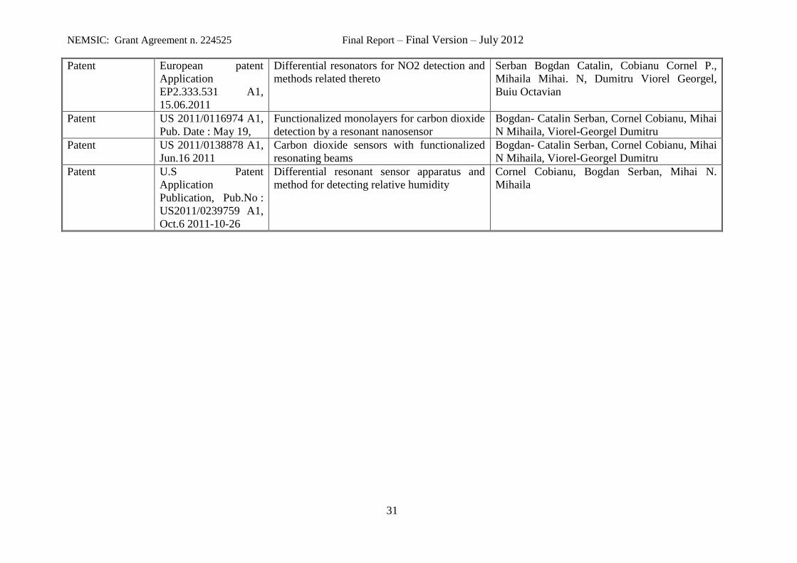
NEMSIC: Grant Agreement n. 224525 Final Report – Final Version – July 2012
31
Patent European patent
Application
EP2.333.531 A1,
15.06.2011
Differential resonators for NO2 detection and
methods related thereto
Serban Bogdan Catalin, Cobianu Cornel P.,
Mihaila Mihai. N, Dumitru Viorel Georgel,
Buiu Octavian
Patent US 2011/0116974 A1,
Pub. Date : May 19,
Functionalized monolayers for carbon dioxide
detection by a resonant nanosensor
Bogdan- Catalin Serban, Cornel Cobianu, Mihai
N Mihaila, Viorel-Georgel Dumitru
Patent US 2011/0138878 A1,
Jun.16 2011
Carbon dioxide sensors with functionalized
resonating beams
Bogdan- Catalin Serban, Cornel Cobianu, Mihai
N Mihaila, Viorel-Georgel Dumitru
Patent U.S Patent
Application
Publication, Pub.No :
US2011/0239759 A1,
Oct.6 2011-10-26
Differential resonant sensor apparatus and
method for detecting relative humidity
Cornel Cobianu, Bogdan Serban, Mihai N.
Mihaila
NEMSIC: Grant Agreement n. 224525 Final Report – Final Version – July 2012
32
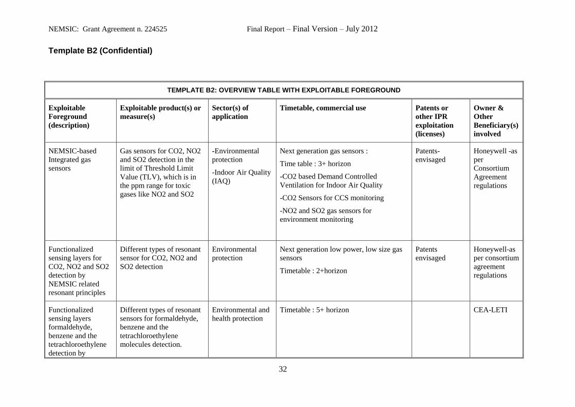
Template B2 (Confidential)
TEMPLATE B2: OVERVIEW TABLE WITH EXPLOITABLE FOREGROUND
Exploitable
Foreground
(description)
Exploitable product(s) or
measure(s)
Sector(s) of
application
Timetable, commercial use Patents or
other IPR
exploitation
(licenses)
Owner &
Other
Beneficiary(s)
involved
NEMSIC-based
Integrated gas
sensors
Gas sensors for CO2, NO2
and SO2 detection in the
limit of Threshold Limit
Value (TLV), which is in
the ppm range for toxic
gases like NO2 and SO2
-Environmental
protection
-Indoor Air Quality
(IAQ)
Next generation gas sensors :
Time table : 3+ horizon
-CO2 based Demand Controlled
Ventilation for Indoor Air Quality
-CO2 Sensors for CCS monitoring
-NO2 and SO2 gas sensors for
environment monitoring
Patents-
envisaged
Honeywell -as
per
Consortium
Agreement
regulations
Functionalized
sensing layers for
CO2, NO2 and SO2
detection by
NEMSIC related
resonant principles
Different types of resonant
sensor for CO2, NO2 and
SO2 detection
Environmental
protection
Next generation low power, low size gas
sensors
Timetable : 2+horizon
Patents
envisaged
Honeywell-as
per consortium
agreement
regulations
Functionalized
sensing layers
formaldehyde,
benzene and the
tetrachloroethylene
detection by
Different types of resonant
sensors for formaldehyde,
benzene and the
tetrachloroethylene
molecules detection.
Environmental and
health protection
Timetable : 5+ horizon
CEA-LETI
NEMSIC: Grant Agreement n. 224525 Final Report – Final Version – July 2012
33
NEMSIC related
resonant principles
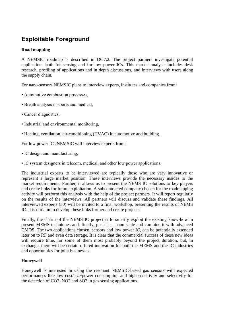
Exploitable Foreground
Road mapping
A NEMSIC roadmap is described in D6.7.2. The project partners investigate potential
applications both for sensing and for low power ICs. This market analysis includes desk
research, profiling of applications and in depth discussions, and interviews with users along
the supply chain.
For nano-sensors NEMSIC plans to interview experts, institutes and companies from:
• Automotive combustion processes,
• Breath analysis in sports and medical,
• Cancer diagnostics,
• Industrial and environmental monitoring,
• Heating, ventilation, air-conditioning (HVAC) in automotive and building.
For low power ICs NEMSIC will interview experts from:
• IC design and manufacturing,
• IC system designers in telecom, medical, and other low power applications.
The industrial experts to be interviewed are typically those who are very innovative or
represent a large market position. These interviews provide the necessary insides to the
market requirements. Further, it allows us to present the NEMS IC solutions to key players
and create links for future exploitation. A subcontracted company chosen for the roadmapping
activity will perform this analysis with the help of the project partners. It will report regularly
on the results of the interviews. All partners will discuss and validate these findings. All
interviewed experts (30) will be invited to a final workshop, presenting the results of NEMS
IC. It is our aim to develop these links further and create projects.
Finally, the charm of the NEMS IC project is to smartly exploit the existing know-how in
present MEMS techniques and, finally, push it at nano-scale and combine it with advanced
CMOS. The two applications chosen, sensors and low power IC, can be potentially extended
later on to RF and even data storage. It is clear that the commercial success of these new ideas
will require time, for some of them most probably beyond the project duration, but, in
exchange, there will be certain offered innovation for both the MEMS and the IC industries
and opportunities for joint businesses.
Honeywell
Honeywell is interested in using the resonant NEMSIC-based gas sensors with expected
performances like low cost/size/power consumption and high sensitivity and selectivity for
the detection of CO2, NO2 and SO2 in gas sensing applications.
NEMSIC: Grant Agreement n. 224525 Deliverable D6.3, Version: 1.0
35
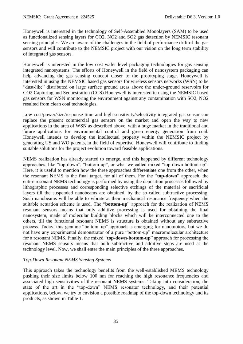
Honeywell is interested in the technology of Self-Assembled Monolayers (SAM) to be used
as functionalized sensing layers for CO2, NO2 and SO2 gas detection by NEMSIC resonant
sensing principles. We are aware of the challenges in the field of performance drift of the gas
sensors and will contribute to the NEMSIC project with our vision on the long term stability
of integrated gas sensors.
Honeywell is interested in the low cost wafer level packaging technologies for gas sensing
integrated nanosystems. The efforts of Honeywell in the field of nanosystem packaging can
help advancing the gas sensing concept closer to the prototyping stage. Honeywell is
interested in using the NEMSIC based gas sensors for wireless sensors networks (WSN) to be
“dust-like” distributed on large surface ground areas above the under-ground reservoirs for
CO2 Capturing and Sequestration (CCS).Honeywell is interested in using the NEMSIC based
gas sensors for WSN monitoring the environment against any contamination with SO2, NO2
resulted from clean coal technologies.
Low cost/power/size/response time and high sensitivity/selectivity integrated gas sensor can
replace the present commercial gas sensors on the market and open the way to new
applications in the area of WSN as described above, with a huge market in the traditional and
future applications for environmental control and green energy generation from coal.
Honeywell intends to develop the intellectual property within the NEMSIC project by
generating US and WO patents, in the field of expertise. Honeywell will contribute to finding
suitable solutions for the project evolution toward feasible applications.
NEMS realization has already started to emerge, and this happened by different technology
approaches, like “top-down”, “bottom-up”, or what we called mixed “top-down-bottom-up”.
Here, it is useful to mention how the three approaches differentiate one from the other, when
the resonant NEMS is the final target, for all of them. For the “top-down” approach, the
entire resonant NEMS technology is performed by using the deposition processes followed by
lithographic processes and corresponding selective etchings of the material or sacrificial
layers till the suspended nanobeams are obtained, by the so-called subtractive processing.
Such nanobeams will be able to vibrate at their mechanical resonance frequency when the
suitable actuation scheme is used. The “bottom-up” approach for the realization of NEMS
resonant sensors means that only additive processing is used for obtaining the final
nanosystem, made of molecular building blocks which will be interconnected one to the
others, till the functional resonant NEMS is structure is obtained without any subtractive
process. Today, this genuine “bottom–up” approach is emerging for nanomotors, but we do
not have any experimental demonstrator of a pure “bottom-up” macromolecular architecture
for a resonant NEMS. Finally, the mixed “top-down-bottom-up” approach for processing the
resonant NEMS sensors means that both subtractive and additive steps are used at the
technology level. Now, we shall enter the main principles of the three approaches.
Top-Down Resonant NEMS Sensing Systems
This approach takes the technology benefits from the well-established MEMS technology
pushing their size limits below 100 nm for reaching the high resonance frequencies and
associated high sensitivities of the resonant NEMS systems. Taking into consideration, the
state of the art in the “top-down” NEMS resonator technology, and their potential
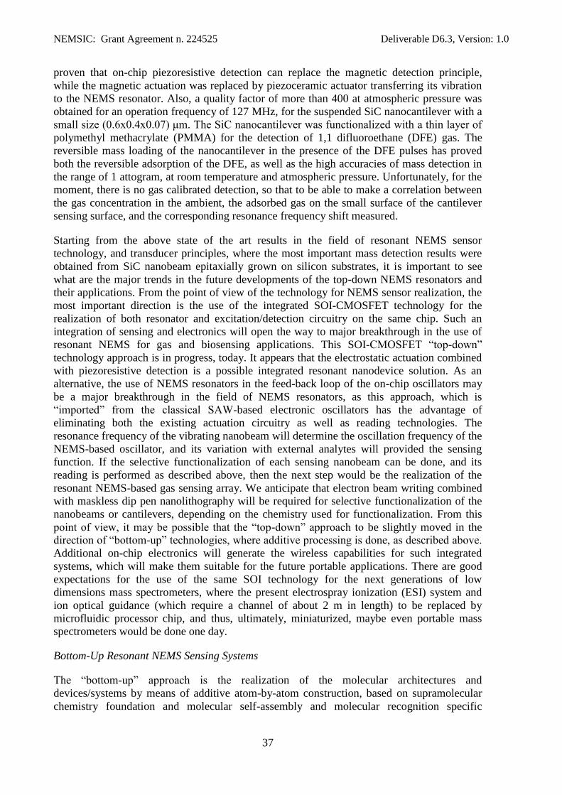
applications, below, we try to envision a possible roadmap of the top-down technology and its
products, as shown in Table 1.
NEMSIC: Grant Agreement n. 224525 Deliverable D6.3, Version: 1.0
36
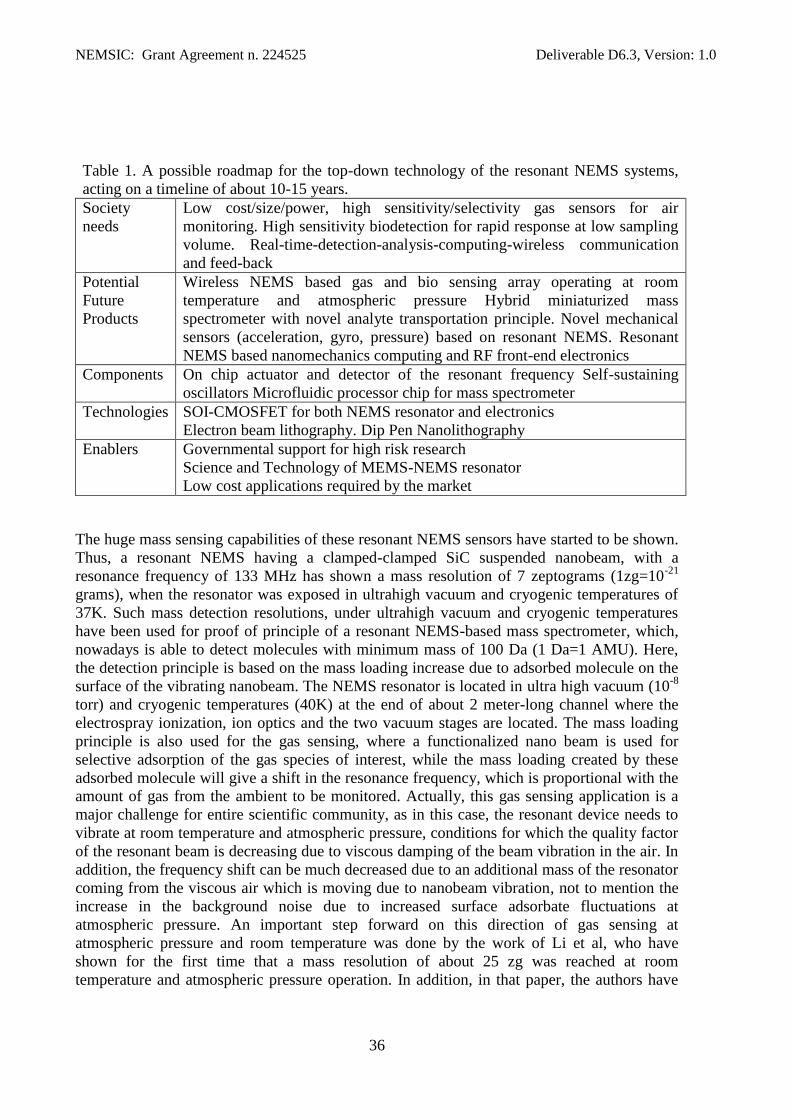
Table 1. A possible roadmap for the top-down technology of the resonant NEMS systems,
acting on a timeline of about 10-15 years.
Society
needs
Low cost/size/power, high sensitivity/selectivity gas sensors for air
monitoring. High sensitivity biodetection for rapid response at low sampling
volume. Real-time-detection-analysis-computing-wireless communication
and feed-back
Potential
Future
Products
Wireless NEMS based gas and bio sensing array operating at room
temperature and atmospheric pressure Hybrid miniaturized mass
spectrometer with novel analyte transportation principle. Novel mechanical
sensors (acceleration, gyro, pressure) based on resonant NEMS. Resonant
NEMS based nanomechanics computing and RF front-end electronics
Components On chip actuator and detector of the resonant frequency Self-sustaining
oscillators Microfluidic processor chip for mass spectrometer
Technologies SOI-CMOSFET for both NEMS resonator and electronics
Electron beam lithography. Dip Pen Nanolithography
Enablers Governmental support for high risk research
Science and Technology of MEMS-NEMS resonator
Low cost applications required by the market
The huge mass sensing capabilities of these resonant NEMS sensors have started to be shown.
Thus, a resonant NEMS having a clamped-clamped SiC suspended nanobeam, with a
resonance frequency of 133 MHz has shown a mass resolution of 7 zeptograms (1zg=10-21
grams), when the resonator was exposed in ultrahigh vacuum and cryogenic temperatures of
37K. Such mass detection resolutions, under ultrahigh vacuum and cryogenic temperatures
have been used for proof of principle of a resonant NEMS-based mass spectrometer, which,
nowadays is able to detect molecules with minimum mass of 100 Da (1 Da=1 AMU). Here,
the detection principle is based on the mass loading increase due to adsorbed molecule on the
surface of the vibrating nanobeam. The NEMS resonator is located in ultra high vacuum (10-8
torr) and cryogenic temperatures (40K) at the end of about 2 meter-long channel where the
electrospray ionization, ion optics and the two vacuum stages are located. The mass loading
principle is also used for the gas sensing, where a functionalized nano beam is used for
selective adsorption of the gas species of interest, while the mass loading created by these
adsorbed molecule will give a shift in the resonance frequency, which is proportional with the
amount of gas from the ambient to be monitored. Actually, this gas sensing application is a
major challenge for entire scientific community, as in this case, the resonant device needs to
vibrate at room temperature and atmospheric pressure, conditions for which the quality factor
of the resonant beam is decreasing due to viscous damping of the beam vibration in the air. In
addition, the frequency shift can be much decreased due to an additional mass of the resonator
coming from the viscous air which is moving due to nanobeam vibration, not to mention the
increase in the background noise due to increased surface adsorbate fluctuations at
atmospheric pressure. An important step forward on this direction of gas sensing at
atmospheric pressure and room temperature was done by the work of Li et al, who have
shown for the first time that a mass resolution of about 25 zg was reached at room
temperature and atmospheric pressure operation. In addition, in that paper, the authors have
NEMSIC: Grant Agreement n. 224525 Deliverable D6.3, Version: 1.0
37
proven that on-chip piezoresistive detection can replace the magnetic detection principle,
while the magnetic actuation was replaced by piezoceramic actuator transferring its vibration
to the NEMS resonator. Also, a quality factor of more than 400 at atmospheric pressure was
obtained for an operation frequency of 127 MHz, for the suspended SiC nanocantilever with a
small size (0.6x0.4x0.07) μm. The SiC nanocantilever was functionalized with a thin layer of
polymethyl methacrylate (PMMA) for the detection of 1,1 difluoroethane (DFE) gas. The
reversible mass loading of the nanocantilever in the presence of the DFE pulses has proved
both the reversible adsorption of the DFE, as well as the high accuracies of mass detection in
the range of 1 attogram, at room temperature and atmospheric pressure. Unfortunately, for the
moment, there is no gas calibrated detection, so that to be able to make a correlation between
the gas concentration in the ambient, the adsorbed gas on the small surface of the cantilever
sensing surface, and the corresponding resonance frequency shift measured.
Starting from the above state of the art results in the field of resonant NEMS sensor
technology, and transducer principles, where the most important mass detection results were
obtained from SiC nanobeam epitaxially grown on silicon substrates, it is important to see
what are the major trends in the future developments of the top-down NEMS resonators and
their applications. From the point of view of the technology for NEMS sensor realization, the
most important direction is the use of the integrated SOI-CMOSFET technology for the
realization of both resonator and excitation/detection circuitry on the same chip. Such an
integration of sensing and electronics will open the way to major breakthrough in the use of
resonant NEMS for gas and biosensing applications. This SOI-CMOSFET “top-down”
technology approach is in progress, today. It appears that the electrostatic actuation combined
with piezoresistive detection is a possible integrated resonant nanodevice solution. As an
alternative, the use of NEMS resonators in the feed-back loop of the on-chip oscillators may
be a major breakthrough in the field of NEMS resonators, as this approach, which is
“imported” from the classical SAW-based electronic oscillators has the advantage of
eliminating both the existing actuation circuitry as well as reading technologies. The
resonance frequency of the vibrating nanobeam will determine the oscillation frequency of the
NEMS-based oscillator, and its variation with external analytes will provided the sensing
function. If the selective functionalization of each sensing nanobeam can be done, and its
reading is performed as described above, then the next step would be the realization of the
resonant NEMS-based gas sensing array. We anticipate that electron beam writing combined
with maskless dip pen nanolithography will be required for selective functionalization of the
nanobeams or cantilevers, depending on the chemistry used for functionalization. From this
point of view, it may be possible that the “top-down” approach to be slightly moved in the
direction of “bottom-up” technologies, where additive processing is done, as described above.
Additional on-chip electronics will generate the wireless capabilities for such integrated
systems, which will make them suitable for the future portable applications. There are good
expectations for the use of the same SOI technology for the next generations of low
dimensions mass spectrometers, where the present electrospray ionization (ESI) system and
ion optical guidance (which require a channel of about 2 m in length) to be replaced by
microfluidic processor chip, and thus, ultimately, miniaturized, maybe even portable mass
spectrometers would be done one day.
Bottom-Up Resonant NEMS Sensing Systems
The “bottom-up” approach is the realization of the molecular architectures and
devices/systems by means of additive atom-by-atom construction, based on supramolecular
chemistry foundation and molecular self-assembly and molecular recognition specific
NEMSIC: Grant Agreement n. 224525 Deliverable D6.3, Version: 1.0
38
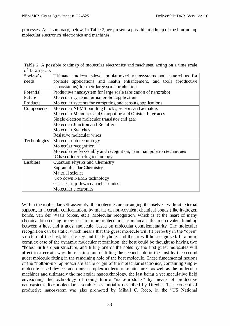
processes. As a summary, below, in Table 2, we present a possible roadmap of the bottom–up
molecular electronics electronics and machines.
Table 2. A possible roadmap of molecular electronics and machines, acting on a time scale
of 15-25 years
Society’s
needs
Ultimate, molecular-level miniaturized nanosystems and nanorobots for
portable applications and health enhancement, and tools (productive
nanosystems) for their large scale production
Potential
Future
Products
Productive nanosystem for large scale fabrication of nanorobot
Molecular systems for nanorobot application
Molecular systems for computing and sensing applications
Components Molecular NEMS building blocks, sensors and actuators
Molecular Memories and Computing and Outside Interfaces
Single electron molecular transistor and gear
Molecular Junction and Rectifier
Molecular Switches
Resistive molecular wires
Technologies Molecular biotechnology
Molecular recognition
Molecular self-assembly and recognition, nanomanipulation techniques
IC based interfacing technology
Enablers Quantum Physics and Chemistry
Supramolecular Chemistry
Material science
Top down NEMS technology
Classical top-down nanoelectronics,
Molecular electronics
Within the molecular self-assembly, the molecules are arranging themselves, without external
support, in a certain conformation, by means of non-covalent chemical bonds (like hydrogen
bonds, van der Waals forces, etc.). Molecular recognition, which is at the heart of many
chemical bio-sensing processes and future molecular sensors means the non-covalent bonding
between a host and a guest molecule, based on molecular complementarity. The molecular
recognition can be static, which means that the guest molecule will fit perfectly in the “open”
structure of the host, like the key and the keyhole, and thus it will be recognized. In a more
complex case of the dynamic molecular recognition, the host could be thought as having two
“holes” in his open structure, and filling one of the holes by the first guest molecules will
affect in a certain way the reaction rate of filling the second hole in the host by the second
guest molecule fitting in the remaining hole of the host molecule. These fundamental notions
of the “bottom-up” approach are at the origin of the molecular electronics, containing single-
molecule based devices and more complex molecular architectures, as well as the molecular
machines and ultimately the molecular nanotechnology, the last being a yet speculative field
envisioning the technology of doing future “nano-products” by means of productive
nanosystems like molecular assembler, as initially described by Drexler. This concept of
productive nanosystem was also promoted by Mihail C. Roco, in the “US National
NEMSIC: Grant Agreement n. 224525 Deliverable D6.3, Version: 1.0
39
Nanotechnology Initiative” as later stage of nanotechnology penetration in the application
domain, where such systems of nanosystems will be used in the factories of the future for the
production of the atomically precise parts of commercial nanosystems.
There is a legitimate question: Why molecular electronics and machines? The answer would
be, yes, we need to go to that direction, because the molecule is the place where the electronic
processes take place, if we think about signal transduction or photosynthesis processes.
Beyond this fundamental motivation, there are practical advantages of molecular electronics
in terms of small size of molecules (1nm up to 100 nm), excellent support from molecular
processing of self-assembly and molecular recognition for “bottom-up” chemical design and
fabrication, to which, other well-developed knowledge like dynamical stereochemistry and
synthetic tailorability are added for the molecular design of the electrical, optical, and
mechanical properties. The molecular electronics has been able to prove the principle
operation of the molecular devices like switches, rectifiers, computational circuits and even
the memory circuits. At the level of proof of principle for molecular electronic circuits, a
memory of 256 bits of RAM performed in a cross bar architecture has been already proven, as
shown in the reference. As an example one can use a molecular switch, which is obtained
from the mechanically interlocked molecular architecture (MIMA) called rotaxane. The
rotaxane is a dumbbell like organic molecule containing a ring-like macrocycle sliding on the
axle of the dumbbell, which is limiting the macrocycle movement at both ends by stoppers of
a larger diameter. The rotaxane based switch is operating like this: when the sliding
macrocycle is at one end, the rotaxane is in an electrically conducting state, while when the
macrocycle is at the other end, the rotaxane is in an electrically not-conductive state. Solid
state rotaxane-based memories in thin films of Langmuir-Blodgett have been already
reported, where the switching of the macrocycle between two different conductive states is
the core of operating principle. The writing of the nano-recording dot was done by applying
locally a positive voltage with the tip of the scanning tunneling microscope.
The family of the MIMA architectures is larger, and is containing other organic components
of the future molecular machines like knotane, acting as a mechanical junction between two
machine components, as well as catenane, acting as a chain made of interconnected rings.
Such MIMA building blocks represent the starting point of the future complex nanomachines.
An initial approach of the rotaxane based molecular motors has been already published, where
the macrocycle of the rotaxane architecture can rotate around the axle. The rotaxane machines
are actuated by chemical or photochemical input signals, and thus muscle functions have been
also reported.
Recent efforts in molecular NEMS are considering biomimetics technologies, where the
forces developed by biological and artificial molecular machines are controlled at this
molecular level, in solid environments, for getting macroscopic effect, like in the case of
skeletal muscles.
It is just a matter of time before the molecular electronics will make a ‘junction” with the
molecular machines for defining the future integrated “molecular intelligence”, where both
sensing and actuation and signal processing to be done at molecular level, in the integrated
molecular nano-machine. In order to reach such level, important milestones of further
understanding the fundamental aspects of electric conduction, sensing and actuation in such
molecular structures and their interfacing with the outside world followed by reliable and
reproducible fabrication of such molecular building blocks of molecular electronics and their
interconnection need to be passed.
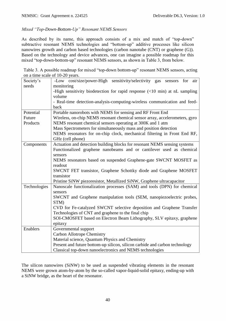
NEMSIC: Grant Agreement n. 224525 Deliverable D6.3, Version: 1.0
40
Mixed “Top-Down-Bottom-Up” Resonant NEMS Sensors
As described by its name, this approach consists of a mix and match of “top-down”
subtractive resonant NEMS technologies and “bottom-up” additive processes like silicon
nanowires growth and carbon based technologies (carbon nanotube (CNT) or graphene (G)).
Based on the technology and device advances, one can imagine a possible roadmap for this
mixed “top-down-bottom-up” resonant NEMS sensors, as shown in Table 3, from below.
Table 3. A possible roadmap for mixed “top-down bottom-up” resonant NEMS sensors, acting
on a time scale of 10-20 years.
Society’s
needs
-Low cost/size/power-High sensitivity/selectivity gas sensors for air
monitoring
-High sensitivity biodetection for rapid response (<10 min) at nL sampling
volume
- Real-time detection-analysis-computing-wireless communication and feed-
back
Potential
Future
Products
Portable nanorobots with NEMS for sensing and RF Front End
Wireless, on-chip NEMS resonant chemical sensor array, accelerometers, gyro
NEMS resonant chemical sensors operating at 300K and 1 atm
Mass Spectrometers for simultaneously mass and position detection
NEMS resonators for on-chip clock, mechanical filtering in Front End RF,
GHz (cell phone)
Components Actuation and detection building blocks for resonant NEMS sensing systems
Functionalized graphene nanobeams and or cantilever used as chemical
sensors
NEMS resonators based on suspended Graphene-gate SWCNT MOSFET as
readout
SWCNT FET transistor, Graphene Schottky diode and Graphene MOSFET
transistor
Pristine SiNW piezoresistor, Metallized SiNW, Graphene ultracapacitor
Technologies Nanoscale functionalization processes (SAM) and tools (DPN) for chemical
sensors
SWCNT and Graphene manipulation tools (SEM, nanopiezoelectric probes,
STM)
CVD for Fe-catalyzed SWCNT selective deposition and Graphene Transfer
Technologies of CNT and graphene to the final chip
SOI-CMOSFET based on Electron Beam Lithography, SLV epitaxy, graphene
epitaxy
Enablers Governmental support
Carbon Allotrope Chemistry
Material science, Quantum Physics and Chemistry
Present and future bottom-up silicon, silicon carbide and carbon technology
Classical top-down nanoelectronics and NEMS technologies
The silicon nanowires (SiNW) to be used as suspended vibrating elements in the resonant
NEMS were grown atom-by-atom by the so-called vapor-liquid-solid epitaxy, ending-up with
a SiNW bridge, as the heart of the resonator.
NEMSIC: Grant Agreement n. 224525 Deliverable D6.3, Version: 1.0
41
The carbon technologies (CNT or G) for nanodevices fabrication has been developed on two
directions: on-chip selective growth or separate growth followed by nanomanipulation of the
CNT or G “foil” to the specific place on the chip surface.
Today, there are already well established technologies for growing on-chip self-assembled
carbon structures to be used for the realization of active devices and sensors. This is the case
of vertical CNT’s obtained selectively and directly on specific areas of the silicon substrates,
where metallic catalysts are previously deposited, or the case of epitaxial graphene obtained
directly on SiC substrate by the sublimation of the silicon atoms from the surface of the SiC
material. The nano-manipulation of the CNT’s or G-foils to the required position on the chip
surface is a labor-intensive process requiring very advanced 3 axis piezoelectric
nanomanipulators tools for transferring the carbon material (CNT or graphene foil) to the
right place on the chip.
Adding the SiNW and carbon technologies to the existing “top-down” resonant NEMS,
previously described has opened the way to improved technologies, which did not further
require the need for SiC suspended nanobeams to be used for the fabrication of high
frequency resonators, and such results will be briefly mentioned here.
For example, in the reference , self-transducing resonant SiNW-NEMS operating at room
temperature and moderate vacuum (1 mtorr) were obtained. In ref. , it is for the first time,
when an on-chip electrostatic actuation and piezoresistive detection (R=100 kΩ) for an
excitation frequency of 40 MHz is reported. In addition, a quality factor of 800 (1200 at high
stress in SiNW, but non-linear response!) is obtained at 300K and 1 mtorr vacuum. Such a
resonant NEMS would generate a mass detection of 500 yg (10-24) (0.6 Da) for 30 nm SiNW,
at an operation frequency of 75 MHz ! Reference is the first paper proving the possibility to
have on-chip actuation and detection for the resonant NEMS, and this was possible for the
case of SiNW resonant nanobeam.
The “carbon” based technologies and their possible integration with IC technology have been
of huge interest in the last decades. Since 1991, when the CNT’s applications were triggered
by the work of Sumio Iijima from NEC, there has been a major interest in controlling CNT’s
fabrication technology and their integration in IC technology as well as in NEMS-based
sensing technology, making the CNT’s a major player for both “Beyond CMOS” technology
and “More than Moore” technologies. CNT is a material of high surface to volume ratio, with
hollow structure and excellent mechanical optical and thermal properties, and a strong
candidate for gas sensing. CNT is used either as “it is” (pristine) or functionalized, or as a
component of matrix nanocomposite. CNT based chemical sensors are using different
principles, like change in the electrical resistance or in the local density of states as a function
of gas to be detected. CNT has been functionalized for detection of different gases, like CO,
CO2, H2S, SO2, NO2, NH3, humidity, methanol, ethanol, 1-propanol, 2-propanol, 1-buthanol,
tertiary- buthanol 1-penthanol, 1-octanol. Challenges with CNT based sensing remains in
terms of still being a costly material and the variation of physical and chemical properties as a
function of preparation process, Related to CNT-based NEMS system, it is worth to mention
here the use of the CNT’s in advanced applications like CNT-based switches, memories and
nanomotors. Resonant NEMS based on CNT and their excitation and detection by coupling
them in the feedback loop of an oscillator has been already reported . CNT applications are
doing rapid steps towards industrial applications, these days.

NEMSIC: Grant Agreement n. 224525 Deliverable D6.3, Version: 1.0
42
The same interest, if not higher has been created by the discovery of the graphene and its
applications, by Andre Geim and Konstantin Novoselov . Graphene is one atom-thick sheet of
carbon atoms arranged in honeycomb lattice. Therefore, graphene is the 2D unit cell of
graphite, where many such graphene “foils” are stacked one over the other. Graphene has
unparalleled strength, stiffness and low mass per unit area. It is a zero-gap material with high
mobility limited by defect scattering. The holes and electron mobility is equal and, for free
standing graphene, it can have a value of about 40000 cm2/Vs, while the electrical resistivity
of graphene can be about 10-6
Ω cm. Its compatibility with 2D IC technology and
lithographically patterning capability, as well as good signal-to-noise ratio in integrated
readout make the graphene an excellent candidate for mixed “top-down-bottom-up” NEMS
resonator technology. The graphene can be prepared either by mechanical exfoliation method
(which remains the best method, for the moment) or by chemical vapor deposition method
from heterogeneous surface reaction between CH4 and H2 on the copper substrate, which is
subsequently etched away, while the graphene layer is embedded in PMMA for its further
transfer on the functional substrate. Such a method was used with the graphene fixed on the
perimeter of a perforated Si3N4 membrane, and the quality factor for such a vibrating
membrane, under tensile stress was very high. Actually, the highest ever product between the
surface/volume ratio and the quality factor (RxQ) was obtained : R*Q=14000 nm-1
, while a
quality factor of 2400 at 300K and 6 mtorr, for a graphene membrane diameter of 22.5 μm
was obtained, in the case of photothermal actuation and interferometric detection. This result
shows that the graphene is an ideal material for future NEMS resonators.
An important step forward in the integration of the carbon technology with silicon
technology has been recently published, where graphene is used as a suspended gate of a FET
transistor, while the field effect is generated in a single wall CNT (SWCNT) located on the
surface of the SiO2/Si substrate. This is the first electron device combining the CNT and the
graphene technology for the realization of a suspended gate graphene and CNT-based FET
device. The CVD-SWCNT is manipulated by SEM to the right position above SiO2/Si. The
electron beam lithography is used for contacting the Pd/Ti metalization to the SWCNT
semiconductor tube. Graphene is mechanically exfoliated from graphite and suspended above
SWCNT. The electrical characterization of the device was performed in vacuum at 100K. The
CNT-FET has an on/off ratio equal to 104 and a minimum resistance of 90kΩ. The 2.1 μm
wide graphene gate has maximum resistance (4.7 kΩ) at Dirac point, while the subthreshold
slope of CNT FET transistor at 100K is 20 mV, i.e. higher than the ideal value at this
temperature, thanks to the technology which is used. In the same time, the graphene
suspended gate FET can be considered as a NEMS resonator, which could work with
electrostatic actuated graphene, as a movable gate for double gate CNT-FET. A major
advantage of this NEMS resonator could be its electronic-tunable resonance frequency by
driving a varying strain in the graphene gate. In addition, non-linear multimode graphene
vibrations would allow mass and position sensing, while the FET used a readout circuit with
its built-in amplification will simplify the resonance frequency detection, in a sensing
application. Therefore, these devices are promising candidate for future mixed “top-down-
bottom-up” NEMS sensors.
IMEC-NL & IMEC
IMEC-NL participates in the NEMSIC funded project because this project fits within a R&D
life cycle approach, running from PhD research over governmental funded projects, industry
sponsored (program or bilaterally organized) toward technology transfer, spin-off or IP
NEMSIC: Grant Agreement n. 224525 Deliverable D6.3, Version: 1.0
43
licensing. As such the results of NEMSIC will form the background for interactions with
industry (locally, European wide and even world-wide) in the field of gas sensing.
The NEMSIC project fits also in the R&D life-cycle approach for IMEC-BE. The IMEC-BE
results of the project will form background for collaborations with the industry, academic
institutions and research institutes in the field of biosensing.
CEA-LETI
CEA-LETI is involved in this project as this institution is aimed at evaluating new concepts
and transferring newly developed technology to industry through technology transfer, spin-off
or IP licensing.
In this project, gas sensors based on NEMS devices have been evaluated as candidates with
strong potential. There will enable to detect with extremely high sensitivities some toxic gases
that could be helpful in both major fields: environment and health.
Our role at CEA-LETI can be to push forward the technology to provide a full integration of
the device including packaging at the wafer scale compatible with the application and to
evaluate the cost of the technology together with the efficiency of new devices. This should
bring a good vision for practical industry exploitation.
In addition, this project could lead to new collaborations with academic/research
organisations and industrial partners at the local or international level.