deliverable 3.5: development of simulation software and...
TRANSCRIPT
SUNFLOWER
“Sustainable Novel Flexible Organic Watts Efficiently Reliable”
Grant agreement No.: 287594 (Integrated Project)
Deliverable 3.5: Development of simulation software and methodology
to analyse and predict the charge transport properties of OPV devices
and modules
Due date of deliverable: 30 July 2014 Actual submission date: 30 September 2014
Start date of project: 1st October 2011 Duration: 48 months
Coordinator FLUXIM
Deliverable Leading Partner FLUXIM
Contributing Partners FLUXIM
Task
Revision UJI (A. Guerrero), CSEM (T. Offermans),
Project co-funded by the European Commission under the Seventh Framework Programme (FP7)
Dissemination Level
PU Public X
PP Restricted to other programme participants (including the Commission Services)
RE Restricted to a group specified by the consortium (including the Commission Services)
CO Confidential, only for members of the consortium (including the Commission Services)

Deliverable 3.5: Development of simulation software and methodology to analyse and predict the charge transport properties of OPV devices and modules GA-No.: 287594
2 / 24
Table of Contents
Table of Contents ................................................................................................................... 2
1 Introduction ...................................................................................................................... 5
2 Electro-absorption ........................................................................................................... 6
2.1 Introduction ............................................................................................................ 6
2.2 Theory .................................................................................................................... 6
2.3 Experimental setup ................................................................................................. 7
2.4 Results ................................................................................................................... 9
2.5 Interpretation ........................................................................................................ 10
2.5.1 Extraction of the built-in potential ....................................................................11
2.6 Summary and conclusion about electro-absorption .............................................. 11
3 Large area simulation of OPVs ...................................................................................... 13
3.1 Introduction .......................................................................................................... 13
3.2 Demonstration of the electrical macro-scale model with our home built solver ..... 14
3.3 Electrical macro-scale model of an OPV module .................................................. 15
3.4 Conclusion ........................................................................................................... 17
4 Numerical solver for impedance spectroscopy ............................................................... 18
4.1 Introduction .......................................................................................................... 18
4.2 Numerical simulation of impedance spectroscopy ................................................ 18
4.2.1 Impact of charge trapping ................................................................................18
4.2.2 Impact of energetic disorder ............................................................................19
4.2.3 Comparison with experiments .........................................................................19
4.3 Conclusion ........................................................................................................... 21
5 Conclusion..................................................................................................................... 22
6 References .................................................................................................................... 23

Deliverable 3.5: Development of simulation software and methodology to analyse and predict the charge transport properties of OPV devices and modules GA-No.: 287594
3 / 24
List of figures and Tables
Figure 1: Schematics of the measurement setup built up for electroabsorption measurements. ..................................................................................................................... 8
Figure 2: Screenshot from the Labview Program that was designed to control the measurement setup and run automated wavelength and/or voltage sweeps. ........................ 8
Figure 3: First Harmonic electroabsorption spectrum at varied Vdc. Curves have been smoothed to emphasise the spectral shape. .........................................................................10
Figure 4: First Harmonic electro-absorption spectra at varied Vac. Curves have been smoothed to emphasise the spectral shape. .........................................................................10
Figure 5: First Harmonic electro-absorption signal at the maximum around 820 nm with varied Vdc. ...........................................................................................................................11
Figure 6: Combination of microscopic and macroscopic electrical models ............................13
Figure 7: Comparison between the Mott Gurney law and the current flowing through the full stack for different electrodes geometries (a). Potential distribution in the top electrode including highly conductive stripes and shunts (b). ...............................................................15
Figure 8: Infra-red picture from dark lock-in thermography (DLIT) revealing several shunts in the OPV module from CSEM. ...............................................................................................16
Figure 9: Schematic of the 2D+1D domain decomposition in the FEM model. .....................16
Figure 10: left: subset of the FEM grid of an OPV module, right: computed power dissipation density in the defective solar module ....................................................................................16
Figure 11: Example capacitance-voltage curves calculated using the new SETFOS 3.4 fast impedance solver for different trap types. .............................................................................18
Figure 12: Simulation of the capacitance versus the frequency for different mobility models (EGDM in green and constant mobility in red) ......................................................................19
Figure 13: Measurement with Paios (a) and simulation with Setfos (b) of the capacitance of an BHJ OPV cell under different light intensities. ..................................................................19
Figure 14: Current voltage characterization of the OPV at different ageing stages. .............20
Figure 15: Measurement with Paios (a) and simulation by Setfos (b) of the capacitance of an OPV for different ageing times. .............................................................................................20
Figure 16: Simulation of the OPV device using SETFOS for different hole doping concentration. .......................................................................................................................21

Deliverable 3.5: Development of simulation software and methodology to analyse and predict the charge transport properties of OPV devices and modules GA-No.: 287594
4 / 24
Abbreviations
EA Electro-absorption
OPV Organic Photovoltaic
FEM Finite element modelling
WF Work-function
Eg Band gap Energy
J-V Current density versus voltage characteristic
Y Admittance
C Capacitance
C0 Geometrical capacitance
Jsc Short Circuit current
Voc Open Circuit Voltage
ℑ Imaginary part

Deliverable 3.5: Development of simulation software and methodology to analyse and predict the charge transport properties of OPV devices and modules GA-No.: 287594
5 / 24
1 Introduction
Organic solar cells might be an important photovoltaics technology in the future, as they promise cheap production and high flexibility for integration. In order to optimize these devices and to understand the physical processes occurring during the device operation, advanced characterization techniques combined with simulation are necessary. In a first part of this report, we present the progress realized concerning the electro-absorption technique that can be used to measure the electric field inside the device structure. In a second part of this deliverable, we report about the development of a 2D+1D solver able to simulate real OPV modules which is important to understand the impact of small defects in the module but also to minimize the losses introduced by non-ideal electrodes. In the last part, we present our progress concerning impedance spectroscopy modelling. Our model is able deal with the distinctive features of organic semiconductor and to consider photo-generated charge carriers.

Deliverable 3.5: Development of simulation software and methodology to analyse and predict the charge transport properties of OPV devices and modules GA-No.: 287594
6 / 24
2 Electro-absorption
2.1 Introduction
Today a major task in organic semiconductor research is to tailor donor and acceptor materials for bulk hetero-junctions, leading to enhanced absorption and charge transport, thus improving efficiencies. Absorption spectroscopy gives insight into the energetic structure of the used materials, as absorption of photons excites electrons to higher states forming excitons. However an electric field influences these energetic states. This physical process is called the Stark effect, leading to a splitting and/or broadening of atomic absorption lines. In the macroscopic case the field can either couple to existing molecular dipole moments µi or induce dipoles which again couple to the field, giving a quadratic response [1]. As the external field is superimposed to the built-in field of the solar cell, this built-in field is accessible by varying the external field. The externally applied field of appropriate magnitude cancels the built-in field and the electro-absorption signal vanishes. Thereby one can access the built-in field in the solar cell. As the electro-absorption effect is small it can only be resolved using sophisticated measurement setups that make use of the lock-in technique. During this project such a dedicated measurement setup was built up and first electro-absorption measurements could be achieved. The measurements were performed on normal organic solar cells without need for specially designed devices.
2.2 Theory
The energetic shift ∆E of an absorption band by the electric field F is given by
∆E(F) =Δ���� = −< Δ�� >− � < Δ���� > (1)
with the change in dipole moment � and the polarizability change ��, giving rise to the linear and quadratic Stark effect, respectively. The energy shift leads to a small change in
absorption Δα, (electroabsorption) which can be expanded into a Taylor series:
Δ� = ���� ⋅ Δ� +
������� ⋅ �Δ��� + ⋯ (2)
Inserting eq. (1) into eq. (2) gives terms linear and quadratic in field with first and second derivative lineshapes. Higher-order terms are neglected as we are dealing with a perturbation effect at small fields. Usually the linear terms can also be ruled out because of the inversion symmetry of disordered conjugated polymer films. Then the permanent molecular dipole moments are randomly oriented and statistically average out to zero. In this approximation, which is followed by most authors, a strict quadratic behaviour of the effect is expected and has been observed many times. Yet, for some materials, this approximation may not be valid, so we use the following equation for our analysis:
Δ� = −Δ�� ⋅ ���� − � Δ���� ⋅ ��
�� + � �Δ���� ⋅ ���
��� (3)
Another motivation for not neglecting the linear contribution is the definition of the dielectric susceptibility appearing in the formula for the absorption coefficient:
� = ��� ⋅ ℑ���� = �
�� ⋅ ℑ !� � + !��� ⋅ � +!�"� ⋅ �� + ⋯# (4)

Deliverable 3.5: Development of simulation software and methodology to analyse and predict the charge transport properties of OPV devices and modules GA-No.: 287594
7 / 24
where c is the light velocity, n is the refractive index and $ is the angular frequency and ℑ the imaginary part. The susceptibility $ relates to the dielectric constant �� as �� = 1 + !. This approach also gives rise to a linear term in F:
Δ� = ��� ⋅ ℑ&!���' ⋅ � + ℑ&!�"�' ⋅ �� + ⋯# (5)
In disordered organic polymer films one usually neglects the linear part in eq. (5) and expects a quadratic field dependence of the effect. A first and second derivative lineshape have been ascribed to Frenkel and CT excitons, respectively [2]. However, this interpretation is controversial, as for example two energetically close-lying Frenkel states can also give a second derivative lineshape [3-5]. Additionally, the mixing of CT and Frenkel excitons is conceivable, further complicating the spectral analysis [6-8]. There has been quite some research on electro-absorption in organic single and molecular crystals [9-14] as well as on the quantum mechanical calculation of their spectra [7,8,15]. Many groups investigated bilayer OLEDs by means of electro-absorption [16-21], mostly focussing on the extraction of the built-in field inside the various layers [22-28]. Recently the electro-absorption analysis on organic photovoltaic cells (OPV) has attracted more interest [12,17,29-40].
2.3 Experimental setup
The measurement of electro-absorption requires a sophisticated experimental setup. In our study the reflectance geometry as proposed by Campbell et al. [23,27] is used, considering the non-transparent aluminum back electrode. A monochromatic beam is guided onto the device and the reflected light, which is in fact the double-transmitted intensity, is measured by a photodiode. A bias voltage is applied and a superimposed small modulation voltage induces periodic changes in the absorption of the organic layer, which is monitored by recording the reflection with the help of the photodiode. The devices we investigate are bulk-heterojunction solar cells, comprising an ITO/PEDOT:PSS anode and an aluminum cathode. The photoactive layer is a 1:2 blend of the donor material PDPP5T (provided by BASF) and the fullerene PCBM-70 with a layer thickness of around 90 nm. The work-functions of the electrodes are around 4.2 eV for aluminum and 5.1 eV for PEDOT:PSS [32,41], giving rise to a built-in voltage of around 0.9 V .

Deliverable 3.5: Development of simulation software and methodology to analyse and predict the charge transport properties of OPV devices and modules GA-No.: 287594
8 / 24
Figure 1: Schematics of the measurement setup built up for electro-absorption measurements.
Figure (1) shows a scheme of the measurement setup. As light source a Xenon lamp (Osram XBO 450W OFR) is used, giving a broad spectrum in the wavelength range from 400-1000 nm. The light passes through a grating monochromator (LOT Oriel Omni 150, 1200 lines/mm) and is focused onto the organic solar cell under an angle of 30°. An external voltage is applied to the solar cell by a function generator (HP 33120A), consisting of an offset voltage and a modulating voltage. The reflected light is then measured with a pre-biased silicon photodiode (Thorlabs DET100A/M) of which the signal is read by a digital multimeter (Picotest M3500A) and a DSP lock-in amplifier (Stanford Research SR830). The control of the whole measurement setup is done using a specially designed Labview program, of which a screenshot is depicted in Fig (2).
Figure 2: Screenshot from the Labview Program that was designed to control the
measurement setup and run automated wavelength and/or voltage sweeps. The multimeter measures the field-independent reflectance (double path transmission, DPT) while the lock-in gives the field-induced change in DPT intensity on the first or second harmonic of the modulation frequency. The electro-absorption signal is then obtained by dividing the modulated signal Δ( by the constant signal I, where I represents the absorbed intensity of light inside the device. Applying the reflectance geometry the measured signal can be approximated using the Lambert-Beer law of absorption:
( = () ⋅ �1 − *�� ⋅ +,-�−2/�� (6)
with the thickness of the organic layer d and the reflectivity R. Neglecting the Kerr effect (field-induced change in reflectivity) one obtains for small absorption changes [42,43] : 011 ≔ �3 ≈ −2/ ⋅ Δ� (7)
Deliverable 3.5: Development of simulation software and methodology to analyse and predict the charge transport properties of OPV devices and modules GA-No.: 287594
9 / 24
Insertion of eq. (5) into eq. (7) gives:
�3 = ����� ⋅ ℑ&!���' ⋅ 5 ⋅ � + ℑ&!�"�' ⋅ 5� ⋅ ��# (8)
with the correction factor f for the effective electric field �677 = 5 ⋅ � inside the dielectric,
usually taken in the Lorentz-approximation [44] 5 = ��8�" , with the refractive index n. By
inserting the applied field � = ��� +�9� :;<�=� and �� = ���� + 2����9�:;<�Ω=� +
� �9�� + � �9�� cos�2B=� the terms on the first and second harmonic of the modulation frequency ,
which are in fact the measured quantities, are computed:
�3 C = ����� ⋅ ℑ&!���' ⋅ 5 ⋅ �9� + ℑ&!�"�' ⋅ 25�����9�# (9)
�3�C = ����� ⋅ Dℑ&!�"�' ⋅
� 5��9�� E (10)
Here we see that the non-neglected linear Stark effect leads to the first term in eq. (9). If one
neglects the !��� contribution to the signal as it is usually assumed for organic materials. We can see that the first harmonic of the electro-absorption signal will be equal to 0 when the DC applied field will cancel. Assuming an homogeneous field inside the device:
��� = � �F9GG −FHI� , the built in potential can then be extracted from electro-absorption
measurements looking at the first harmonic by sweeping the applied bias F9GG. The
measurement of the built-in voltage using electro-absorption can then be used to check the validity of the experimental setup and it can also be seen as a complementary experiment to extract this important parameters.
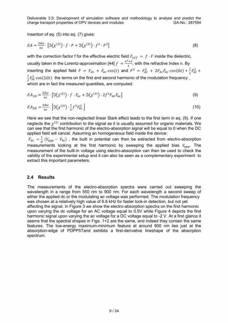
2.4 Results
The measurements of the electro-absorption spectra were carried out sweeping the wavelength in a range from 550 nm to 900 nm. For each wavelength a second sweep of either the applied dc or the modulating ac voltage was performed. The modulation frequency was chosen at a relatively high value of 6.6 kHz for faster lock-in detection, but not yet affecting the signal. In Figure 3 we show the electro-absorption spectra on the first harmonic upon varying the dc voltage for an AC voltage equal to 0.5V while Figure 4 depicts the first harmonic signal upon varying the ac voltage for a DC voltage equal to -2 V. At a first glance it seems that the spectral shapes in Figs. 1+2 are the same, and indeed they contain the same features. The low-energy maximum-minimum feature at around 800 nm lies just at the absorption-edge of PDPP5Tand exhibits a first-derivative lineshape of the absorption spectrum.

Deliverable 3.5: Development of simulation software and methodology to analyse and predict the charge transport properties of OPV devices and modules GA-No.: 287594
10 / 24
Figure 3: First Harmonic electro-absorption spectrum at varied Vdc. Curves have been
smoothed to emphasise the spectral shape.
Figure 4: First Harmonic electro-absorption spectra at varied Vac. Curves have been smoothed to emphasise the spectral shape.
2.5 Interpretation
Equation 9 predicts a linear dependency of the first harmonic of the electro-absorption signal versus the AC modulation of the applied bias. This observation is validated by the Figure 4
that shows the �3 C for different amplitude of �9�. Indeed we can see on Figure 4 that the amplitude of oscillations scales with the Vac.
However if the !��� contribution is neglected, Equation 9 also predicts a linear dependency of �3 C versus the DC applied field which is not verified in the figure 3. This observation
Deliverable 3.5: Development of simulation software and methodology to analyse and predict the charge transport properties of OPV devices and modules GA-No.: 287594
11 / 24
raises the question on the validity of the inversion symmetry of the polymer film used in this OPV.
2.5.1 Extraction of the built-in potential
Figure 5: First Harmonic electro-absorption signal at the maximum around 820 nm with
varied Vdc.
An analysis of the Vdc variation can be used to extract the built-in voltage of the device. In Fig. (5) we show the �3 C signal at 820 nm (which corresponds to the maximum of signal) versus Vdc. As expected from equation 9, we observe a linear variation of the first harmonic of the electro-absorption signal versus the applied DC bias in the negative region. For higher applied bias than Vbi, we can notice that the electro-absorption signal remains at 0, this can be a consequence of the screening of the electric field inside the device due to the injection of charges.
Therefore, following equation 9 and neglecting the !��� contribution, we can extract the built-in potential: the straight line that is obtained in the negative bias range can be extrapolated to zero. This gives a built-in voltage of around 1.1V in this case, which can be related to the difference in work-function of the two electrodes. Moreover, the linearity of the electro-absorption signal versus the steady state applied bias shows that the device is free of charges in this regime leading to an homogenous electric field.
2.6 Summary and conclusion about electro-absorption
Based on previous studies in the literature we built up an own measurement setup specifically designed for electro-absorption spectroscopy. In order to investigate thin-film organic solar cells with aluminum electrodes, the reflection geometry has to be used. The change in absorption is then measured using a lock-in amplifier. We could demonstrate the applicability of this setup for organic solar cells. First measurements can be used to extract the built-in voltage. A more detailed study using different electrode materials could further support the analysis approach.
The fitting of the electro-absorption spectra using derivatives of the original absorption spectrum can give insight into the static molecular dipole moments and may thus help to identify a potentially preferred orientation of molecules. This signal could then be registered versus degradation time to monitor the ordering of the organic material in the device.

Deliverable 3.5: Development of simulation software and methodology to analyse and predict the charge transport properties of OPV devices and modules GA-No.: 287594
12 / 24
Also, as this method gives a direct access to the electric field inside the device, it could be used to monitor the concentration of traps during the ageing process but also to study the electric field in PN junction forming the recombination layer in Tandem cells.
This technique could also be used to probe the electric field in the two sub-cells of a tandem stack independently.
This study has raised the question on the validity of the common approximation consisting in
neglecting the !��� contribution for symmetry reasons. However further investigations, for example doing this measurement on a standard P3HT solar cell, would be necessary before giving final conclusions.
In future work the electro-absorption measurement could be correlated with electrical simulation from SETFOS.

Deliverable 3.5: Development of simulation software and methodology to analyse and predict the charge transport properties of OPV devices and modules GA-No.: 287594
13 / 24
3 Large area simulation of OPVs
3.1 Introduction
From an electrical point of view, an OPV can be regarded as a succession of thin (few tens of nanometers) semiconducting layers sandwiched between an anode and a cathode on the scale of the centimeter. One of these electrodes requires being transparent so that the light can enter the device, however transparent electrodes are fairly bad conductors leading to an inhomogeneous potential distribution in the large area electrodes and thus to electrical losses. So far, there is no unique modeling method able to simulate the full device on these different scales in a reasonable time. It is thus mandatory to combine and link several simulation techniques where each of them can be used to model the physic of the device on a specific length scale. Due to the high aspect ratio (large area electrode versus the through plane thickness) of an OPV, the electrical model can be split up into a 2D FEM model, to solve the current distribution in the large area electrodes, and a 1D microscopic model, to compute the current flowing vertically in the device solving the semiconductor equations.
Figure 6: Combination of microscopic and macroscopic electrical models
Figure 6 describes the multi-scale electrical model workflow
First the user provides several electrical parameters to the microscopic electrical model.
These parameters describe the microscopic nature of the different semiconductor materials
used in the OPV stack i. e: the band gap Eg, the mobility µ, the density of states N0 L as well
as the workfunction WF of the two electrodes material. Given these input parameters, the
microscopic electrical model computes the J-V characteristic of the small OPV for different

Deliverable 3.5: Development of simulation software and methodology to analyse and predict the charge transport properties of OPV devices and modules GA-No.: 287594
14 / 24
temperatures. This J-V characteristic will be used as an input parameter for the 2D macro-
scale FEM solver.
On the thermal point of view the user needs to provide the heat conduction coefficient of all
the layers as well as the thermal convection coefficient of the layers in contact with air (h)
which usually are derived from the interface orientation and material parameters of air. As it
can be demonstrated, the thermal flux entering the electrodes (ϕ) is an analytical function of
the temperature of the two electrodes and of the heat generated in the thin film layer stack, a
numerical micro-scale modeling tool is thus not necessary for the thermal part.
In a second step, the macro-scale electro-thermal 2D FEM solver is used to compute the
potential distribution in the electrodes as well as the current flowing through the large OPV
by solving the standard flux continuity equation in the electrodes for the electrical current. In
this equation the current flowing vertically will be considered as a source term for the
electrical part of the model. The macro-scale model requires several input parameters:
1. The J-V characteristic of the small OPV provided by the microscopic electrical model.
2. The geometry of the two electrodes.
3. The electrical conductivity of the different materials used in the electrodes: σ and the
boundary conditions.
3.2 Demonstration of the electrical macro-scale model with our home built solver
We developed a 2+1D FEM solver for the electrical macro-scale model. In order to test the
non-linear 2D FEM solver we have assumed that the J-V characteristics of the ‘small’ OPV
could be approximated by the well-known Mott Gurney law
J = KL M. � O�
PQ ,
where V represents the potential difference between the cathode and the anode, ε the
dielectric constant of the semiconductor, L the thickness of the semiconductor layer and µ the
mobility in the semiconductor. We could then compute the currents flowing through the whole
device (Figure 7 (a)) revealing the electrical losses introduced by the non-ideal electrode.
Indeed if the electrodes were perfect conductors we should have found the Mott-Gurney law
(red curve). It was also possible to compute the potential distribution for different electrode
geometries (Figure 7 (b)) comprising of thin, highly conductive stripes aligned horizontally
and/or vertically. The current density scaled to the device area approximates the Mott-
Gurney law in case of highly conductive electrodes thanks to the metal grid. Further, we
could simulate the effect of shunts between the two electrodes (Figure 7(b)). Namely they
affect the distribution of the electric potential in the electrode.

Deliverable 3.5: Development of simulation software and methodology to analyse and predict the charge transport properties of OPV devices and modules GA-No.: 287594
15 / 24
(a)
(b)
Figure 7: Comparison between the Mott Gurney law and the current flowing through the full
stack for different electrodes geometries (a). Potential distribution in the top electrode
including highly conductive stripes and shunts (b).
3.3 Electrical macro-scale model of an OPV module
In this section we make use of this 2D+1D modelling approach to simulate a degraded OPV module. We investigate mechanical failure modes of such all-plastic encapsulated flexible solar modules.
Simulations are compared with measurements using high-resolution lock-in thermography in the dark (D-LIT) (figure 8 and 10), which revealed localized defects after shipment. Our analysis considers the layout of the entire module and is therefore also able to parametrically optimize the device geometry (metal finger widths, cell width, etc.).
In Figure 9 we show a schematic cross-section of the device we have simulated. We made use of a parameterized analytical law (j1(V)) to fit the experimental current density versus voltage characteristic for the active area. Concerning the defective area we have assumed that there was an interconnection between the top and bottom electrode which was modelled by a low resistivity (j2(v)) between the top and bottom electrode in this region.

Deliverable 3.5: Development of simulation software and methodology to analyse and predict the charge transport properties of OPV devices and modules GA-No.: 287594
16 / 24
Figure 8: Infra-red picture from dark lock-in thermography (DLIT) revealing shunts in the OPV module.
Figure 9: Schematic of the 2D+1D domain decomposition in the FEM model.
In Figure 10 we have made use of the multi-physics FEM software SESES to run the simulations, but a similar approach is developed in a special-purpose software and demonstrated at FLUXIM (see previous section).
Figure 10: left: subset of the FEM grid of an OPV module, right: computed power dissipation density in the defective solar module

Deliverable 3.5: Development of simulation software and methodology to analyse and predict the charge transport properties of OPV devices and modules GA-No.: 287594
17 / 24
3.4 Conclusion
We have shown a successful proof of principle simulation with a new FEM software prototype, but need further investigations and developments to market this tool. In the following of this project we plan to integrate more closely the micro-scale electrical model already included in SETFOS with the 2D FEM model. Indeed, so far, the 2D FEM tool only allows the user to import an analytical law to describe the J-V curve of the ‘small’ OPV device. We plan to enable the possibility to import an arbitrary J-V characteristic in the 2D FEM solver opening the way to a total integration of the 2D FEM solver into SETFOS. Also a user friendly interface is currently developed in order to commercialize this new product.
Moreover we have demonstrated that this approach can be used to simulate real OPV modules and to study the impact of defects and imperfections on the module operation.
This simulation tool will be used in WP5, to optimize the design of the high conductive stripes for the demonstrators.

Deliverable 3.5: Development of simulation software and methodology to analyse and predict the charge transport properties of OPV devices and modules GA-No.: 287594
18 / 24
4 Numerical solver for impedance spectroscopy
4.1 Introduction
Impedance spectroscopy of organic semiconductor devices is becoming an attractive characterization method, since this relatively simple measurement technique reveals charge transport properties at different time scales. Several demonstrations have been reported by Universitad Jaume I (UJI), Spain, that this technique is a powerful approach to study key physical processes occurring during the operation of an OPV like recombination, charge trapping but also charge transport in the device. The basic idea of this technique is to superimpose a sinusoidal voltage of small amplitude onto a static applied bias. The frequency of the sinusoidal voltage can be varied to study and investigate physical processes on different time scales. In this task we have extended our numerical drift-diffusion solver already implemented in the commercial software Setfos to operate in the frequency regime. Simulations of impedance spectroscopy data (Z, C and G as a function of frequency or offset voltage) are then fast and reliable. This new feature allows considering charge trapping, photo-generation of electron-hole pairs and energetic disorder of the transport bands (HOMO and LUMO). The commercial version of this simulation software Setfos 3.4 was released in December 2013 by Fluxim.
The simulated admittance Y of a device can be split between a real and an imaginary part:
R = S + T. $. U,
where R represents the resistance of the device and C the capacitance.
4.2 Numerical simulation of impedance spectroscopy
4.2.1 Impact of charge trapping
Trap states are defined as localized, isolated states with low energy with respect to the transport energy. They reside in the low energy tail of the density of states (DOS). Trap states are known to strongly affect electrical device properties, therefore modeling of their influence is critical for predictive device simulation. Recently, SETFOS was extended with a fast impedance solver with trapping support. It allows to quickly calculate all types of responses. Figure 11 presents example capacitance-frequency curves calculated using SETFOS 3.4 for the cases of slow and fast traps, with comparison to the trapless case.
Figure 11: Example capacitance-voltage curves calculated using the new SETFOS 3.4 fast impedance solver for different trap types.

Deliverable 3.5: Development of simulation software and methodology to analyse and predict the charge transport properties of OPV devices and modules GA-No.: 287594
19 / 24
As one can notice, the trap dynamics strongly influences the capacitance signal at low frequencies in case of slow traps (i.e. when the trap capture rate is small). Combining electrical characterization and numerical simulation of impedance spectroscopy data it is therefore possible to study the charge trap dynamics. These simulation results, using Setfos 3.4, are consistent with the simulations shown in the publication by E. Knapp and B. Ruhstaller [47], revealing the accuracy of the SETFOS solver.
4.2.2 Impact of energetic disorder
Figure 12: Simulation of the capacitance versus the frequency for different mobility models (EGDM in green and constant mobility in red)
The energetic disorder of the HOMO and LUMO can also be simulated as shown in Figure 12. We notice that the energetic disorder impacts the capacitance mainly at low frequencies, leading to an increase of the capacitance.
4.2.3 Comparison with experiments
In this section we have compared results from capacitance simulations with measured capacitance using PAIOS for a bulk heterojunction OPV cell provided by Belectric OPV.
In Figure 13 we notice that the impact of photo-generation of charge carriers in an OPV can be nicely reproduced by Setfos simulations.
(a) (b)
Figure 13: Measurement with Paios (a) and simulation with Setfos (b) of the capacitance of an BHJ OPV cell under different light intensities.

Deliverable 3.5: Development of simulation software and methodology to analyse and predict the charge transport properties of OPV devices and modules GA-No.: 287594
20 / 24
In a last step, an OPV from Belectric was exposed to a synthetic atmosphere. The aging of the device was monitored as a function of the absorbance loss. In Figure 14, we observe that the performances of the cell tend to decrease with the ageing. The loss of absorbance of the device is too low to explain the performance losses. In figure 15, we show that the variation of the capacitance signal versus the ageing can be nicely reproduced by introducing some hole dopants in the device. The presence of hole dopants in the aged device has been confirmed by CELIV characterizations [45]. Finally we have introduced some hole dopants in the simulation of an IV curve (figure 16) and we could observe the same trend as in the experiments: a loss of JSC.
Therefore using small signal analysis, we could identify the origin of degradation mechanisms occurring in the device.
Figure 14: Current voltage characterization of the OPV at different ageing stages.
(a) (b)
Figure 15: Measurement with Paios (a) and simulation by Setfos (b) of the capacitance of an OPV for different ageing times.

Deliverable 3.5: Development of simulation software and methodology to analyse and predict the charge transport properties of OPV devices and modules GA-No.: 287594
21 / 24
Figure 16: Simulation of the OPV device using SETFOS for different hole doping concentration.
4.3 Conclusion
A impedance solver has been implemented in the commercialized simulation software SETFOS (from version 3.4). This solver allows fast and reliable simulations of impedance spectroscopy of OPV cells. The impact of carrier photo-generation, energetic disorder of transport bands and traps can be simulated. This solver has been successfully compared with experiments validating our simulation and measurement approach. It has also been used to study the degradation mechanisms occurring in BHJ OPV cells, which has been used in workpackage 4.
We will extend this solver to multilayers devices, this will be used for studying the physical mechanism happening in the recombination layer within Work-package 2.

Deliverable 3.5: Development of simulation software and methodology to analyse and predict the charge transport properties of OPV devices and modules GA-No.: 287594
22 / 24
5 Conclusion
In this deliverable we have shown our current status concerning large area modelling of OPV modules, impedance spectroscopy simulations and electro-absorption characterization. While our impedance spectroscopy solver is already commercialized, our large area solver is still under development but a proof of principle has been demonstrated in this report. Finally the electro-absorption technique still requires further investigations that will assess the benefits of this complementary technique.
The impedance spectroscopy solver and the large area OPV simulator are planned to be used in the other work-packages.
Deliverable 3.5: Development of simulation software and methodology to analyse and predict the charge transport properties of OPV devices and modules GA-No.: 287594
23 / 24
6 References
[1] Weiser, “Electroabsorption spectroscopy on p-conjugated polymers”, (World Scientific Publ. ,Singapore, 1997) Chap. 12, p. 318.
[2] L. Sebastian, G. Weiser, and H. Bässler, Chem. Phys. 61, 125 (1981). [3] Slawik, J. Chem. Phys. 107, 7114 (1997). [4] Slawik, J. Chem. Phys. 111, 7576 (1999). [5] P. J. Brewer, Internal Field Screening in Polymer Light Emitting Diodes, Ph.D. thesis, Imperial College London (2005). [6] Petelenz, Chem. Phys. Lett. 47, 603 (1977). [7] P. Petelenz, Org. El. 5, 115 (2004). [8] M. Ho_mann, K. Schmidt, T. Fritz, T. Hasche, V. Agranovich, and K. Leo, Chem. Phys. 258,73 (2000). [9] Sebastian, Chem. Phys. 62, 447 (1981). [10] G. Weiser, J. Lumin. 110, 189 (2004). [11] Horvath, Mol. Cryst. Liq. Cryst. 256, 79 (1994). [12] W. Guo, Electroabsorption Spectroscopy of Quasi-one-dimensional Organic Molecular Crystals, Ph.D. thesis, Technische Universit at Dresden (2003). [13] Möller, Synth. Met. 116, 305 (2001). [14] Sebastian, Chem. Phys. 64, 396 (1979). [15] Petelenz, Lecture Series on Computer and Computational Sciences 6, 1 (2006). [16] V. Bodrozic, M. Roberts, N. Phillips, J. H. Burroughes, S. Mian, and F. Cacialli, J. Appl. Phys. 101, 084507 (2007). [17] C. Lungenschmied, G. Dennler, H. Neugebauer, N. S. Sariciftci, and E. Ehrenfreund, Appl. Phys. Lett. 89, 223519 (2006). [18] P. J. Brewer, P. A. Lane, A. J. deMello, D. D. C. Bradley, and J. C. deMello, Adv. Funct. Mater. 14, 562 (2004). [19] P. J. Brewer, A. J. deMello, J. C. deMello, P. A. Lane, D. D. C. Bradley, R. Fletcher, and J. O'Brien, J. Appl. Phys. 99, 114502 (2006). [20] P. J. Brewer, P. A. Lane, J. Huang, A. J. deMello, D. D. C. Bradley, and J. C. deMello, Phys. Rev. B 71, 205209 (2005). [21] Horvath, Phys. Rev. B 51, 2751 (1995). [22] I. H. Campbell, M. D. Joswick, and I. D. Parker, Appl. Phys. Lett. 67, 3171 (1995). [23] I. H. Campbell, J. P. Ferraris, T. W. Hagler, M. D. Joswick, I. D. Parker, and D. L. Smith, Polym. Adv. Technol. 8, 417 (1997). [24] C. M. Heller, I. H. Campbell, D. L. Smith, N. N. Barashkov, and J. P. Ferraris, J. Appl. Phys. 81, 3227 (1997). [25] R. J. de Vries, S. L. M. van Mensfoort, R. A. J. Janssen, and R. Coehoorn, Phys. Rev. B 81, 125203 (2010). [26] T. M. Brown, J. S. Kim, R. H. Friend, F. Cacialli, R. Daik, and W. J. Feast, Appl. Phys. Lett. 75, 1679 (1999). [27] T. M. Brown, R. H. Friend, I. S. Millard, D. J. Lacey, T. Butler, J. H. Burroughes, and F. Cacialli, J. Appl. Phys. 93, 6159 (2003). [28] K. Book, H. B assler, A. Elschner, and S. Kirchmeyer, Org. El. 4, 227 (2003). [29] Lungenschmied, Electroabsorption in Organic Diodes, Master's thesis, Linz Institute of Organic Solar Cells (2004). [30] P. Lane, J. Rostalski, C. Giebeler, S. Martin, D. Bradley, and D. Meissner, Sol. Energy Mater. Sol. Cells 63, 3 (2000). [31] T. Drori, J. Holt, and Z. V. Vardeny, Phys. Rev. B 82, 075207 (2010). [32] B. Zimmermann, M. Glatthaar, M. Niggemann, M. Riede, and A. Hinsch, Thin Solid Films 493, 170 (2005). [33] Hiromitsu, Jap. J. Appl. Phys. 46, 7241 (2007). [34] Hiromitsu, J. Appl. Phys. 94, 2434 (2003). [35] Hiromitsu, Synth. Met. 137, 1358 (2003). [36] Navarro, Proc. SPIE 6999, 69991K (2008). [37] S. Kogler, Charge Modulation Spectroscopy, Master's thesis, Linz (2010). [38] Ooi, J. Mater. Chem. 18, 1644 (2008).

Deliverable 3.5: Development of simulation software and methodology to analyse and predict the charge transport properties of OPV devices and modules GA-No.: 287594
24 / 24
[39] Drori, Phys. Rev. Lett. 101, 037401 (2008). [40] Lungenschmied, Injektions- und Rekombinationsph anomene in organischen Dünnschichtbauelementen, Ph.D. thesis, Linz (2006). [41] Brewer, Phys. Rev. B 74, 115202 (2006). [42] G. Weiser, Phys. Stat. Sol. (a) 18, 347 (1973). [43] Phillips, Phys. Rev. B 40, 9751 (1989). [44] Kalinowski, Chem. Phys. 182, 341 (1994). [45] T. Lanz, M. Bonmarin, T. Offermans, B. Ruhstaller, 6th International Conference on Hybrid and Organic Photovoltaics, Lausanne, Switzerland (2014) [46] S. Altazin, M. Neukom, F. Müller, S. Züfle, E. Knapp, B. Ruhstaller, 6th International Exhibition and Conference for the Printed Electronics Industry, Munich, Germany (2014) [47] E. Knapp, B. Ruhstaller, "The role of shallow traps in dynamic characterization of organic semiconductor devices", J. of Appl. Phys., Volume 112, Issue 2, (2012)