letter - ece.ucsb.edustrukov/papers/2015/nature2015.pdf · play the parts of axons and dendrites...
TRANSCRIPT

LETTERdoi:10.1038/nature14441
Training and operation of an integrated neuromorphicnetwork based on metal-oxide memristorsM. Prezioso1*, F. Merrikh-Bayat1*, B. D. Hoskins1*, G. C. Adam1, K. K. Likharev2 & D. B. Strukov1
Despite much progress in semiconductor integrated circuit techno-logy, the extreme complexity of the human cerebral cortex1, with itsapproximately 1014 synapses, makes the hardware implementationof neuromorphic networks with a comparable number of devicesexceptionally challenging. To provide comparable complexity whileoperating much faster and with manageable power dissipation,networks2 based on circuits3,4 combining complementary metal-oxide-semiconductors (CMOSs) and adjustable two-terminal res-istive devices (memristors) have been developed. In such circuits,the usual CMOS stack is augmented with one3 or several4 crossbarlayers, with memristors at each crosspoint. There have recently beennotable improvements in the fabrication of such memristive cross-bars and their integration with CMOS circuits5–12, including firstdemonstrations5,6,12 of their vertical integration. Separately, dis-crete memristors have been used as artificial synapses in neuro-morphic networks13–18. Very recently, such experiments have beenextended19 to crossbar arrays of phase-change memristive devices.The adjustment of such devices, however, requires an additionaltransistor at each crosspoint, and hence these devices are muchharder to scale than metal-oxide memristors11,20,21, whose nonlinearcurrent–voltage curves enable transistor-free operation. Here wereport the experimental implementation of transistor-free metal-oxide memristor crossbars, with device variability sufficiently lowto allow operation of integrated neural networks, in a simple net-work: a single-layer perceptron (an algorithm for linear classifica-tion). The network can be taught in situ using a coarse-grain varietyof the delta rule algorithm22 to perform the perfect classificationof 3 3 3-pixel black/white images into three classes (representingletters). This demonstration is an important step towards muchlarger and more complex memristive neuromorphic networks.
In a hybrid CMOS/memristor circuit, the CMOS subsystem con-tacts each wire, and hence can address each memristor on the add-oncrossbar(s), using a specific ‘CMOL’ area-distributed interface3,4. Thebasic idea of hybrid neuromorphic networks—so-called CrossNets2—is to use this opportunity to connect CMOS-implemented hardwaremodels of neuron bodies with the memristive crossbar(s), whose wiresplay the parts of axons and dendrites and whose memristors mimicbiological synapses. The simple, two-terminal, transistor-free topologyof metal-oxide memristors may enable CrossNets to achieve extremelyhigh density—much higher than that of pure-CMOS neuromorphicnetworks (including those based on CMOS-modelled memristors23
,
floating-gate24 and ferroelectric25 memory cells), and even higher thanthat of their biological prototypes. For example, a CrossNet based on ahybrid CMOS/memristor circuit with five layers of 30-nm-pitch cross-bars, two memristors per synapse, and 104 synapses per neural cellwould have an areal density of about 25 million cells per square cen-timetre, that is, higher than that in the human cerebral cortex, at com-parable average connectivity1. Estimates show that such CrossNets mayalso provide comparable power efficiency, at a much higher operationspeed—for example, an intercell signal transfer delay of about 0.02 ms
(compared to about 10 ms in biological systems) at an easily manage-able energy dissipation rate of about 1 W cm22.
However, the practical implementation of such networks is still verychallenging, owing to the specific physical mechanism of resistancechange in most prospective metal-oxide-based memristors—areversible modulation of the concentration profile of oxygenvacancies11,20,21. On the positive side, the atomic scale of the vacancyposition modulation implies the possibility of memristor scaling downto few-nanometre dimensions, which has been confirmed by recentexperiments26,27. On the negative side, such a small scale makes thedevice-to-device reproducibility of device parameters, most impor-tantly the voltage required for memristor electroforming andswitching20,21, difficult to achieve with the currently used fabricationtechnologies. Device variability is the main reason why the only(to our knowledge) demonstrations of memristive neuromorphicnetworks were based on disconnecting each memristor from thecrossbar for individual forming, using either a crossbar with external(off-chip) wires18, or an individual switch transistor at each cross-point19. Both these approaches are incompatible with the goal ofreaching the extremely high density of neuromorphic networks dis-cussed above.
The main goal of this work was an experimental demonstration of afully operational neural network based on an integrated, transistor-free crossbar with metal-oxide memristors. To reach this goal, a largereduction of memristor variability was essential, and to achieve it, weused binary-oxide Al2O3/TiO2 2 x stacks (see inset to Fig. 1b). Theirfabrication procedure was generally close to that described in ref. 27,but with the important difference of using low-temperature (,300 uC)reactive sputtering for film deposition, which enables monolithicthree-dimensional integration. The stack was first optimized by con-ducting an exhaustive experimental search over a range of titaniumdioxide compositions and layer thicknesses (from 5 nm to 100 nm) tofind the parameter range providing the lowest forming voltages.Within that range, the device performance—most importantly thememristor uniformity and the current–voltage curve nonlinearity—was further optimized by varying the aluminium oxide thickness from1 nm to 5 nm (Supplementary Information Section 1).
The main feature of such optimized junctions is their low variability(Supplementary Figs 3 and 4). In addition, other important character-istics of the 200 nm 3 200 nm formed devices are also desirable: theON/OFF current ratios of above four orders of magnitude (at 60.1 V),high nonlinearity of the current–voltage curves (with the current at theswitching voltage more than ten times the current at half of the switch-ing voltage), a switching endurance of at least 5,000 cycles, an esti-mated memory retention of at least ten years at room temperature,low forming (,2 V) and switching (,1.5 V) voltages, and relati-vely low operation currents of between ,100 nA and ,100 mA (seeSupplementary Fig. 1).
The optimized technology was then used to fabricate an integratedmemristive crossbar with 12 3 12 devices (Fig. 1), with a few process
*These authors contributed equally to this work.
1Department of Electrical and Computer Engineering, University of California at Santa Barbara, Santa Barbara, California 93106, USA. 2Department of Physics and Astronomy, Stony Brook University,Stony Brook, New York 11794, USA.
G2015 Macmillan Publishers Limited. All rights reserved
7 M A Y 2 0 1 5 | V O L 5 2 1 | N A T U R E | 6 1

modifications to increase the metal electrode thickness, so that the lineresistances were reduced to about 800 V for the top layer of the cross-bar and 600V for its bottom layer. The crossbars retained the excellentuniformity of virgin (pre-formed) crossbar-integrated devices (seeSupplementary Figs 3, 4 and 5), allowing individual electric formingand tuning of each memristor. The electroforming was performed bygrounding the corresponding bottom electrode and applying a cur-rent-controlled ramp-up to the top electrode, while leaving all otherline potentials floating (Supplementary Fig. 4). To minimize currentleakage during the subsequent forming of other devices, each formedmemristor was immediately switched into its low-current (OFF) state.The measured individual characteristics of the formed memristorswere mostly similar to those of stand-alone devices, except for a some-what smaller ( 100) ON/OFF current ratio. This difference may bepartly explained by current leakage through other crosspoints at themeasurements, and partly by the somewhat smaller switching voltagesused for the crossbar to lower the risk of device damage. In addition,some deviations from the optimal device performance could becaused by the electron-beam evaporation of thicker electrodes, whichrequired breaking of the vacuum, as opposed to the fully in situ sput-tering of single device layers, and their subsequent annealing (seeSupplementary Information).
The fabricated memristive crossbar was used to implement a simpleartificial neural network with the top-level (functional) scheme shownin Fig. 2. This is a single-layer perceptron22 with ten inputs and threeoutputs, fully connected with 10 3 3 5 30 synaptic weights (Fig. 2b).
As the scheme shows, the perceptron’s outputs fi (with i 5 1, 2, 3) arecalculated as nonlinear ‘activation’ functions:
fi~ tanh bIið Þ ð1Þof the vector-by-matrix product components:
Ii~X10
j~1
WijVj ð2Þ
Here Vj with j 5 1,…,9 are the input signals, V10 is a constant bias, bis a parameter controlling the function’s nonlinearity, and Wij areadjustable (trainable) synaptic weights. Such a network is sufficientfor performing, for example, the classification of 3 3 3-pixel black-and-white images into three classes, with nine network inputs(V1,…,V9) corresponding to the pixel values. We tested the networkon a set of N 5 30 patterns, including three stylized letters (‘z’, ‘v’and ‘n’) and three sets of nine noisy versions of each letter, formedby flipping one of the pixels of the original image (see Fig. 2c).Because of the very limited size of the set, it was used for both trainingand testing.
Physically, each input signal was represented by a voltage Vj equal toeither 10.1 V or 20.1 V, corresponding, respectively, to the black orwhite pixel, while the bias input V10 was equal to 20.1 V. Such codingmakes the benchmark input set balanced, in particular ensuring thatthe sum of all input signals across all patterns of a particular classis close to zero, which speeds up the convergence process28. Tosustain this balance at the network’s output as well, each synapse
–2.0 –1.5 –1.0 –0.5 0.0 0.5 1.0
–600
–500
–400
–300
–200
–100
0
100
200
Voltage, V (V)
Reset
Set
0 20 40 60 80 100 120 140
0
10
20
30
40
50
601.1 V
1.2 V
1.3 V
–1.1 V
–1.2 V
–1.3 V
c
2 μm
a bTop electrodes
Bo
tto
m e
lectr
od
es
Ab
s[Δ
G (μS
)]
Cu
rren
t, I
(μA
)
Pt (60 nm)
Pt (60 nm)
Ta (5 nm)
Ti (15 nm)
TiO2 – x
(30 nm)
Al2O
3 (4 nm)
SiO2/Si
Conductance, G (μS)
Figure 1 | Memristor crossbar. a, Integrated 12 3 12 crossbar with an Al2O3/TiO2 2 x memristor at each crosspoint. b, A typical current–voltage curve of aformed memristor. c, Absolute values of conductance change under the effect of
500-ms voltage pulses of two polarities, as a function of the initial conductance,for various pulse amplitudes. The inset in b shows the device cross-sectionschematically.
d
c
Bias
Inputneurons
Output neuronsa
V1
V4
V7
V2
V5
V8
V3
V6
V9
V10 V
10
Vj(n)
V2
V1
W1,1 I
1
I2
I3
f1
f2
f3
W3,10
Weights
Σ
Σ
z
n
v
Ideal With one flipped pixel
b
Σ
Calculate
ΔijEq. (4)
Setn = 1Δij = 0
Desired class fi(g)(n)
Lastpattern?
No
Yes
n = n +1
Calculatefi(n)
Eq. (1)
CalculateIi(n)
Eq. (2)
Next epoch
End ofepoch
UpdateweightsEq. (5)
3 × 3 binaryimage
Training set:
initialize Wij
{Vj(n), fi(g)(n)}n = 1
N
Figure 2 | Pattern classification experiment (top-level description). a, Inputimage. b, The single-layer perceptron for classification of 3 3 3 binary images.c, The used input pattern set. d, The flow chart of one epoch of the used in situ
training algorithm. In d, the grey-shaded boxes show the steps implementedinside the crossbar, while those with solid black borders denote the only stepsrequired to perform the classification operation.
RESEARCH LETTER
G2015 Macmillan Publishers Limited. All rights reserved
6 2 | N A T U R E | V O L 5 2 1 | 7 M A Y 2 0 1 5
was implemented with two memristors, so that the total number ofmemristors in the crossbar was 30 3 2 5 60. Using external electronicsto enforce the virtual ground conditions on each column line, and tosubtract currents flowing in the adjacent columns to form a differentialoutput signal Ii, we ensured that Ohm’s law applied to each columnof the crossbar gave a result identical to equation (2), with differen-tial weights:
Wij~Gzij {G{
ij ð3Þ
where G+ij is the effective conductance of each memristor, namely the
I/V ratio at voltage 0.1 V. For our devices, these effective conductanceswere in the range 10–100 mS, so that currents Ii were of the order of afew microamperes. Activation functions—see equation (1)—werealso implemented, using external electronics, with the slope b 5 2 3
105 A21 chosen according to the recommendation in ref. 28, con-firmed by our own computer simulations (Supplementary Fig. 10).
The network was trained in situ, that is, without using its externalcomputer model, using the Manhattan update rule29, which is essen-tially a coarse-grain, batch-mode variation of the usual delta rule ofsupervised training22. At each iteration (‘epoch’) of this procedure,sketched in Fig. 2d, patterns from the training set were applied,one by one, to the network’s input, and its outputs fi(n), where n is
the pattern number, were used to calculate the delta-rule weightincrements:
Dij nð Þ~di nð ÞVj nð Þwith
di nð Þ~ f (g)i nð Þ{fi nð Þh i df
dI
����I~Ii(n) ð4Þ
Here f gð Þi nð Þ is the target value of the ith output for the nth input
pattern. (In our system these values were chosen to be 10.85 for theoutput corresponding to the correct pattern class, and 20.85 for theoutput corresponding to the wrong class.) Once all N patterns of thetraining set had been applied, and all Dij(n) calculated, the synapticweights were modified using the following Manhattan update rule:
DWij~g sgnXN
n~1
Dij nð Þ ð5Þ
where g is a constant that scales the training rate. (The only differencebetween the Manhattan update rule from the batch-mode delta rule isthe binary quantization, expressed in equation (5) by the ‘sgn’ func-tion, which simplifies the hardware implementation of the delta rule.
Differential pair
A A A A
ba
Bias
Pattern (‘z’)
V =
sgn[ΔW] =++−−++–−+−
+−−−+−−−−+
−−−−−+++++
0
0 0 0 0
c
0
0
0
V1
+VR
–VW
+/2
–VW
+/2
0
0
–VW
+/2
–VW
+/2
–VW
+/2
+VW
+/2
+VR
+VR
+VR
+VR
–VR
–VR
–VR
–VR
–VR
I1+ I
1– I
2+ I
2– I
3+ I3
–
G1,1
+
G1,2
+
G1,10
+
G3,1
+
G3,2
+
G3,10
+
G3,1
–
G3,2
–
G3,10
–
G1,1
–
G1,2
–
G1,10
–
V2
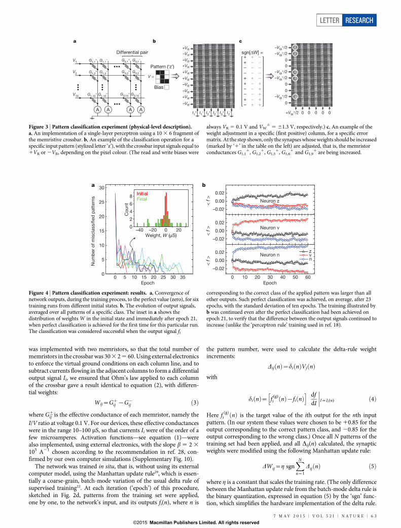
V10
Figure 3 | Pattern classification experiment (physical-level description).a, An implementation of a single-layer perceptron using a 10 3 6 fragment ofthe memristive crossbar. b, An example of the classification operation for aspecific input pattern (stylized letter ‘z’), with the crossbar input signals equal to1VR or 2VR, depending on the pixel colour. (The read and write biases were
always VR 5 0.1 V and VW6 5 61.3 V, respectively.) c, An example of the
weight adjustment in a specific (first positive) column, for a specific errormatrix. At the step shown, only the synapses whose weights should be increased(marked by ‘1’ in the table on the left) are adjusted, that is, the memristorconductances G1,1
1, G1,21, G1,5
1, G1,61 and G1,9
1 are being increased.
–0.02
0.00
0.02
–0.02
0.00
0.02
0 10 20 30 40 50 60
–0.02
0.00
0.02 z v n
Neuron v
Neuron z
EpochEpoch
Neuron n
0 5 10 15 20 25 30 350
5
10
15
20
25
30
–40 –20 0 200
2
4
6
8
Co
un
t
Weight, W (μS)
InitialInitialFinal
ba
< f
><
f >
< f
>
Num
ber
of
mis
cla
ssifi
ed
patt
ern
s
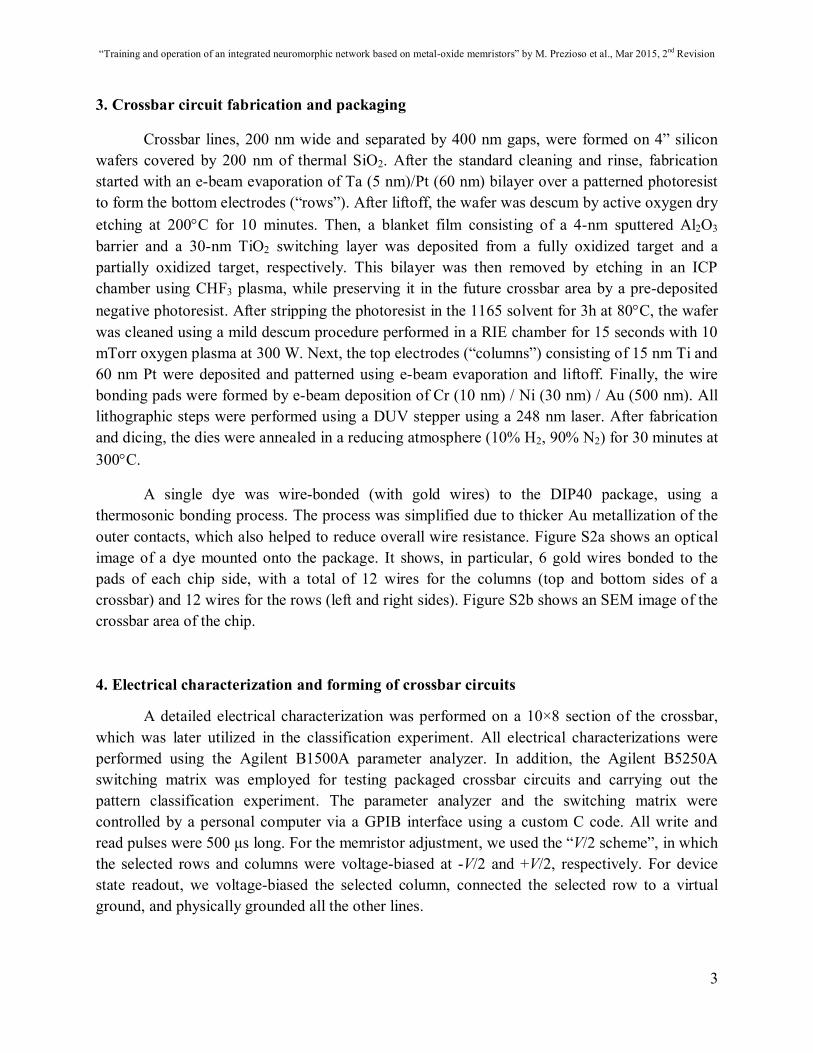
Figure 4 | Pattern classification experiment: results. a, Convergence ofnetwork outputs, during the training process, to the perfect value (zero), for sixtraining runs from different initial states. b, The evolution of output signals,averaged over all patterns of a specific class. The inset in a shows thedistribution of weights W in the initial state and immediately after epoch 21,when perfect classification is achieved for the first time for this particular run.The classification was considered successful when the output signal fi
corresponding to the correct class of the applied pattern was larger than allother outputs. Such perfect classification was achieved, on average, after 23epochs, with the standard deviation of ten epochs. The training illustrated byb was continued even after the perfect classification had been achieved onepoch 21, to verify that the difference between the output signals continued toincrease (unlike the ‘perceptron rule’ training used in ref. 18).
LETTER RESEARCH
G2015 Macmillan Publishers Limited. All rights reserved
7 M A Y 2 0 1 5 | V O L 5 2 1 | N A T U R E | 6 3

Physically, in our system the weights were modified in parallel foreach column of the crossbar (corresponding to a certain value of indexi in the above formulas), using two sequential voltage pulses. Namely,first a ‘set’ pulse with amplitude VW
1 5 1.3 V was applied to increasethe conductances of the synapses whose DG values, calculated fromequation (5), were positive; then a ‘reset’ pulse VW
2 5 21.3 V wasapplied to the remaining synapses of that column (see Fig. 3c). Thisfixed-amplitude pulse procedure followed the Manhattan update ruleonly approximately, because the actual training rate DG depends onthe initial conductance G of the memristor (see Fig. 1c andSupplementary Fig. 6). (For G 5 20 mS, DG was close to 160 mS forthe set pulse and 25 mS for the reset pulse, while for G 5 65 mS, thechanges were close, respectively, to 124 mS and 255 mS.) Owing to thespecific (though quite representative11) switching dynamics of ourdevices, the best classification performance was achieved when thememristors had been initialized somewhere in the middle of theirconductance range, around 35 mS (Supplementary Fig. 7b). At suchinitialization, the perfect classification was reached, on average, after23 training epochs (see Fig. 4).
In summary, here we have experimentally demonstrated an artificialneural network using memristors integrated into a dense, transistor-free crossbar circuit. This crossbar performed, on the physical (Ohm’slaw) level, the analogue vector-by-matrix multiplication of equations(2) and (3), which is by far the most computationally intensive part ofthe operation of any neuromorphic network used repeatedly in thesame environment. The other operations, described by equations (1),(4) and (5), were performed by external electronics, but they are muchless critical for network performance, and in future, larger CrossNetsmay be (at least partly) assisted by CMOS subsystems. This is animportant step towards the effective analogue-hardware implementa-tion of much more complex neuromorphic networks, from multilayer-perceptron classifiers with deep learning30 to elaborate CrossNet-basedcognitive systems. Recent experiments27 with similar but smaller (dis-crete) devices imply that such circuits may be scaled down to devices of30 nm across or less, that is, to networks with a density of approxi-mately 1010 synapses per square centimetre in each crossbar layer.
Received 16 December 2014; accepted 19 March 2015.
1. Mountcastle, V. B. The Cerebral Cortex (Harvard Univ. Press, 1998).2. Likharev, K. K. CrossNets: neuromorphic hybrid CMOS/nanoelectronic networks.
Sci. Adv. Mater. 3, 322–331 (2011).3. Likharev, K. K. Hybrid CMOS/nanoelectronic circuits: opportunities and
challenges. J. Nanoelectron. Optoelectron. 3, 203–230 (2008).4. Strukov, D. B. & Williams, R. S. Four-dimensional address topology for circuits with
stacked multilayer crossbar arrays. Proc. Natl Acad. Sci. USA 106, 20155–20158(2009).
5. Xia, Q. et al. Memristor-CMOS hybrid integrated circuits for configurable logic.Nano Lett. 9, 3640–3645 (2009).
6. Chevallier, C. J.et al.0.13mm 64Mbmulti-layeredconductivemetal-oxidememory.Int. Solid-State Circuits Conf. 10, 260–261 (2010).
7. Miyamura, M. et al. Programmable cell array using rewritable solid-electrolyteswitch integrated in 90 nm CMOS. Int. Solid-State Circuits Conf. 11, 228–229(2011).
8. Kawahara, A. et al. An 8Mb multi-layered cross-point ReRAM macro with 443MB/swrite throughput. Int. Solid-State Circuits Conf. 12, 432–434 (2012).
9. Kim, G. H. et al. 32332 crossbar array resistive memory composed of a stackedSchottky diode and unipolar resistive memory. Adv. Funct. Mater. 23, 1440–1449(2013).
10. Kim, K.-H. et al. A functional hybrid memristor crossbar-array/CMOS system fordata storage and neuromorphic applications. Nano Lett. 12, 389–395 (2012).
11. Yang, J. J., Strukov, D. B. & Stewart, D. R. Memristive devices for computing. NatureNanotechnol. 8, 13–24 (2013).
12. Liu, T. et al. A 130.7-mm 2-layer 32-Gb ReRAM memory device in 24-nmtechnology. IEEE J. Solid-State Circuits 49, 140–153 (2014).
13. Jo, S. H. et al. Nanoscale memristor device as synapse in neuromorphic systems.Nano Lett. 10, 1297–1301 (2010).
14. Chanthbouala, A. et al. A ferroelectric memristor. Nature Mater. 11, 860–864(2012).
15. Seo,K.et al.Analogmemoryand spike-timing-dependent plasticity characteristicsof a nanoscale titanium oxide bilayer resistive switching device. Nanotechnology22, 254023 (2011).
16. Ohno, T. et al. Short-term plasticity and long-term potentiation mimicked in singleinorganic synapses. Nature Mater. 10, 591–595 (2011).
17. Ziegler, M. et al. An electronic version of Pavlov’s dog. Adv. Funct. Mater. 22,2744–2749 (2012).
18. Alibart, F., Zamanidoost, E. & Strukov, D. B. Pattern classification by memristivecrossbar circuitswith ex-situ and in-situ training.NatureCommun. 4, 2072 (2013).
19. Eryilmaz, S. B. et al. Brain-like associative learning using a nanoscale non-volatilephase change synaptic device array. Front. Neurosci. 8, 205 (2014).
20. Waser, R., Dittman, R., Staikov, G. & Szot, K. Redox-based resistive switchingmemories. Adv. Mater. 21, 2632–2663 (2009).
21. Wong, H. S. P. et al. Metal–oxide RRAM. Proc. IEEE 100, 1951–1970 (2012).22. Hertz, J., Krogh, A. & Palmer, R. G. Introduction to the Theory of Neural Computation
(Perseus, 1991).23. Pershin, Y. V. & Di Ventra, M. Experimental demonstration of associative memory
with memristive neural network. Neural Netw. 23, 881–886 (2010).24. Hasler, J. & Marr, B. Finding a roadmap to achieve large neuromorphic hardware
systems. Front. Neurosci. 7, 118 (2013).25. Kaneko, Y., Nishitani, Y. & Ueda, M. Ferroelectric artificial synapses for recognition
of a multishaded image. IEEE Trans. Electron. Dev. 61, 2827–2833 (2014).26. Pi, S., Lin, P. & Xia, Q. Cross point arrays of 8 nm 3 8 nm memristive devices
fabricated with nanoimprint lithography. J. Vacuum Sci. Technol. B 31, 06FA02–1(2013).
27. Govoreanu, B. et al. Vacancy-modulated conductive oxide resistive RAM (VMCO-RRAM). IEDM Tech Dig. 10.2. 1–4http://dx.doi.org/10.1109/IEDM.2013.6724599(2013).
28. LeCun, Y., Bottou, L., Orr, G. B. & Muller, K.-R. Efficient backprop. Lect. NotesComput. Sci. 7700, 9–48 (2012).
29. Schiffmann, W., Joost, M. & Werner, R. Optimization of the BackpropagationAlgorithm for Training Multilayer Perceptrons https://citeseerx.ist.psu.edu/viewdoc/download?doi510.1.1.53.6869&rep5rep1&type5pdf (TechnicalReport, Institute of Physics, University of Koblenz, 1994).
30. Krizhevsky, A., Sutskever, I. & Hinton, G. E. ImageNet classification with deepconvolutional neural networks. Neural Inf. Process. Systems 12, 1097–1105(2012).
Supplementary Information is available in the online version of the paper.
Acknowledgements We acknowledge useful discussions with F. Alibart, I. Kataeva,W. Lu, L. Sengupta, S. Stemmer, and E. Zamanidoost. This work was supported by theAFOSR under the MURI grant FA9550-12-1-0038, by DARPA under contract numberHR0011-13-C-0051UPSIDE via BAE Systems, and by the DENSO Corporation, Japan.
Author Contributions M.P., F.M.-B., B.D.H., K.K.L., and D.B.S. designed the research.M.P., B.D.H., and G.C.A. performed fabrication and device testing. M.P. and F.M.-B.performed pattern classifier experiments. All authors discussed and interpretedresults. M.P., K.K.L., and D.B.S. wrote the manuscript. K.K.L. and D.B.S. advised on allparts of the project.
Author Information Reprints and permissions information is available atwww.nature.com/reprints. The authors declare no competing financial interests.Readers are welcome to comment on the online version of the paper. Correspondenceand requests for materials should be addressed to M.P. ([email protected])and D.B.S. ([email protected]).
RESEARCH LETTER
G2015 Macmillan Publishers Limited. All rights reserved
6 4 | N A T U R E | V O L 5 2 1 | 7 M A Y 2 0 1 5

“Training and operation of an integrated neuromorphic network based on metal-oxide memristors” by M. Prezioso et al., Mar 2015, 2nd Revision
1
Supplementary Information
1. Material and device stack optimization
Lower electroforming voltages reduce the electrical stress as well as current overshoot during the forming, which is a known risk factor contributing to device variability1. It had been noticed that lower forming voltages may be achieved in devices with higher conductivity, obtained by a combination of oxide layer thickness reduction and stoichiometry adjustment2,3. In our experiments, the oxygen concentration was continuously reduced by controlling the oxygen flow rate during the layer growth to the point at which resistive switching nearly ceased. The switching voltages of such devices were close to, or less than the electroforming voltage. However, many devices could not be turned off after switching and instead were shunted, or in some cases exhibited spontaneous complementary resistive switching. The observed nonlinearity of the I-V curves of such devices was also not large enough for crossbar operation. To address these issues, an Al2O3 layer was added to the device stack. (Multilayers and bilayers had been used previously to improve device performance4,5.) An excessive increase of the Al2O3 barrier thickness causes an increase of the forming voltage, so that an optimum thickness had to be selected. As a result of material and stack optimization, the most suitable values of thicknesses for TiO2-x and Al2O3 layers have turned out to be close to respectively, 30 nm and 4 nm (Fig. S1b).
2. Electrical characterization of single devices
To perform electrical characterization, single 200 nm × 200 nm devices of the dog-bone geometry (Fig. S1b) were fabricated first. (The inset in that figure shows the material stack parameters; note that they are slightly different from those in the crossbar-integrated devices – cf. the inset in Fig. 1b of the main text.) Figure S1a shows typical switching curves of such single devices, obtained by applying bipolar voltage sweeps. (To exhibit the I-V curve nonlinearity better, Fig. S1a also shows Ohmic currents for several resistance values.)
Figure S1c shows representative endurance test results for single devices. The data are obtained by repeatedly (over 5,000 times total) applying a sequence of set (-2 V, 500 µs), readout (0.1 V, 1 ms), reset (2 V, 500 µs), and again readout voltage pulses to a single device. The figure does not reflect the fact that approximately 7% of the negative pulses failed to switch off the device; however, this behavior may be attributed to an imperfect endurance setup rather than any deep device problem. This conclusion is supported by the fact that the device was being switched after each failure event. Some aging (in the form of a slight degradation of the ON/OFF dynamic range) is also visible, but generally the devices are rather robust. For example, during our experiments with the crossbar circuit, each of its memristors had been subjected, on the average, to 200,000 set/reset pulses even prior to the successful classification experiment.

“Training and operation of an integrated neuromorphic network based on metal-oxide memristors” by M. Prezioso et al., Mar 2015, 2nd Revision
2
As customary in nonvolatile memory technology, the retention test shown in Fig. S1d was carried out with a sample heated to 350 K. The device was first switched into a certain resistive state, and then its resistance was measured repeatedly by applying a 100 mV bias every 2 seconds during a 50,000-second time interval. Such retention measurements were carried out for ON (highly conductive), OFF (highly resistive), and some intermediate states. Based on the measurements, the retention at room temperature is expected to exceed 10 years.
2 V2 V
0 1000 2000 3000 4000 5000
104
105
106
Pulse
Res
ista
nce
On state
Off stateIntermediate
0 12.5 25 37.5 50
108
107
106
105
Time ks
Cur
rent
A
Ta (5 nm)
Pt (35 nm)
Al2O3 (4 nm)
TiO2-x (30 nm)
Ti (15 nm)
Pt (25 nm)
SiO2/Si1.0 0.5 0.0 0.5 1.0
1010
108
106
104
Voltage V
Cur
rent
A
1 MΩ
100 kΩ
10 kΩ
1 kΩ
c
b
d
First
Last
a
Res
ista
nce
(Ω)
Cur
rent
(A)
Cur
rent
(A)
Pulse # Time (ks)
Voltage (V)
Figure S1. Isolated Pt/TiO2-x/Al2O3/Pt memristive devices: (a) typical switching and electroforming behavior of a single device, (b) micrograph of a single device and its stack's structure, (c) switching endurance under a stream of ±2 V, 500-µs pulses, and (d) retention of 3 initial states at 350 K. To highlight the data trends, large markers on panels (c) and (d) show the results of every 100th measurement at the endurance test, and of every 1,000th measurement at the retention test. Note that panel (d) shows significantly lower OFF state currents (and hence much higher ON/OFF current ratio) as compared to those of panels (a) and (c) due to higher voltages applied to reset the device.
“Training and operation of an integrated neuromorphic network based on metal-oxide memristors” by M. Prezioso et al., Mar 2015, 2nd Revision
3
3. Crossbar circuit fabrication and packaging
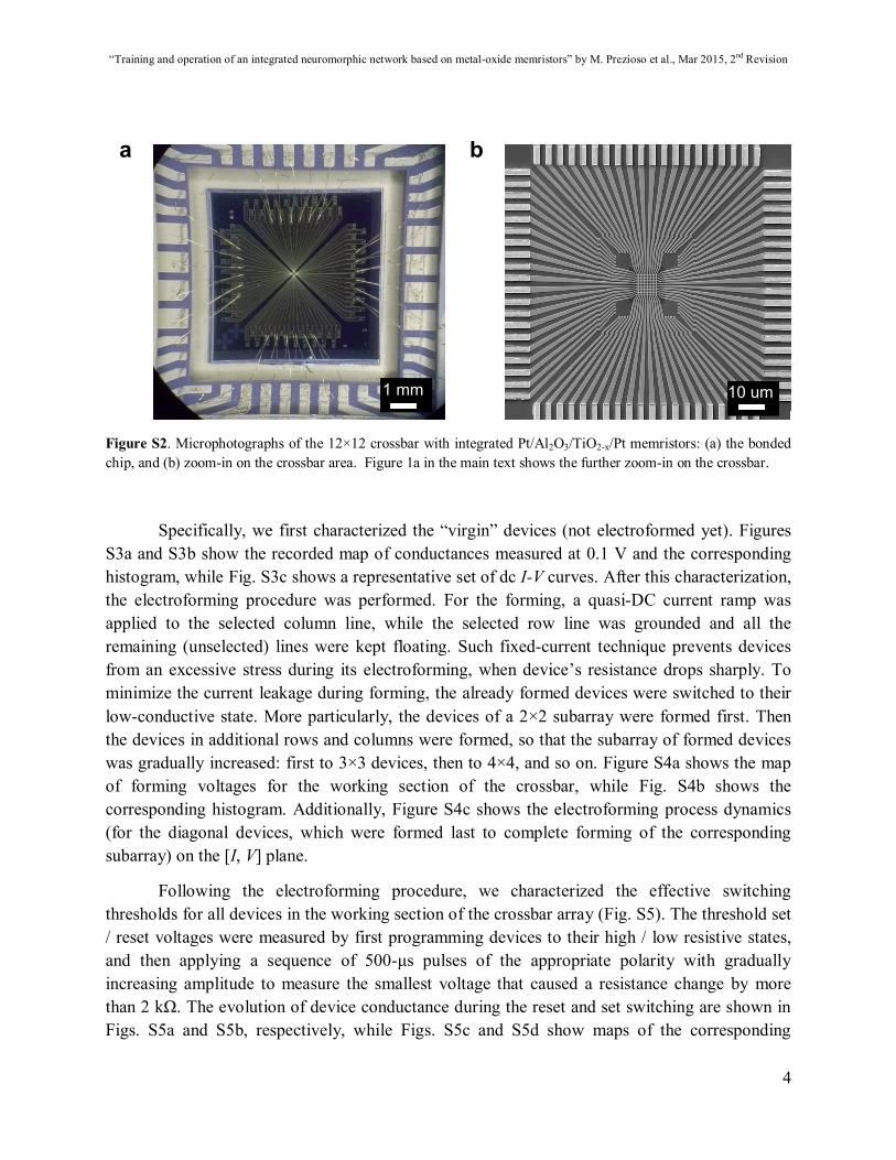
Crossbar lines, 200 nm wide and separated by 400 nm gaps, were formed on 4” silicon wafers covered by 200 nm of thermal SiO2. After the standard cleaning and rinse, fabrication started with an e-beam evaporation of Ta (5 nm)/Pt (60 nm) bilayer over a patterned photoresist to form the bottom electrodes (“rows”). After liftoff, the wafer was descum by active oxygen dry etching at 200C for 10 minutes. Then, a blanket film consisting of a 4-nm sputtered Al2O3 barrier and a 30-nm TiO2 switching layer was deposited from a fully oxidized target and a partially oxidized target, respectively. This bilayer was then removed by etching in an ICP chamber using CHF3 plasma, while preserving it in the future crossbar area by a pre-deposited negative photoresist. After stripping the photoresist in the 1165 solvent for 3h at 80C, the wafer was cleaned using a mild descum procedure performed in a RIE chamber for 15 seconds with 10 mTorr oxygen plasma at 300 W. Next, the top electrodes (“columns”) consisting of 15 nm Ti and 60 nm Pt were deposited and patterned using e-beam evaporation and liftoff. Finally, the wire bonding pads were formed by e-beam deposition of Cr (10 nm) / Ni (30 nm) / Au (500 nm). All lithographic steps were performed using a DUV stepper using a 248 nm laser. After fabrication and dicing, the dies were annealed in a reducing atmosphere (10% H2, 90% N2) for 30 minutes at 300C.
A single dye was wire-bonded (with gold wires) to the DIP40 package, using a thermosonic bonding process. The process was simplified due to thicker Au metallization of the outer contacts, which also helped to reduce overall wire resistance. Figure S2a shows an optical image of a dye mounted onto the package. It shows, in particular, 6 gold wires bonded to the pads of each chip side, with a total of 12 wires for the columns (top and bottom sides of a crossbar) and 12 wires for the rows (left and right sides). Figure S2b shows an SEM image of the crossbar area of the chip.
4. Electrical characterization and forming of crossbar circuits
A detailed electrical characterization was performed on a 10×8 section of the crossbar, which was later utilized in the classification experiment. All electrical characterizations were performed using the Agilent B1500A parameter analyzer. In addition, the Agilent B5250A switching matrix was employed for testing packaged crossbar circuits and carrying out the pattern classification experiment. The parameter analyzer and the switching matrix were controlled by a personal computer via a GPIB interface using a custom C code. All write and read pulses were 500 μs long. For the memristor adjustment, we used the “V/2 scheme”, in which the selected rows and columns were voltage-biased at -V/2 and +V/2, respectively. For device state readout, we voltage-biased the selected column, connected the selected row to a virtual ground, and physically grounded all the other lines.
“Training and operation of an integrated neuromorphic network based on metal-oxide memristors” by M. Prezioso et al., Mar 2015, 2nd Revision
4
a b
1 mm 10 um
Figure S2. Microphotographs of the 12×12 crossbar with integrated Pt/Al2O3/TiO2-x/Pt memristors: (a) the bonded chip, and (b) zoom-in on the crossbar area. Figure 1a in the main text shows the further zoom-in on the crossbar.
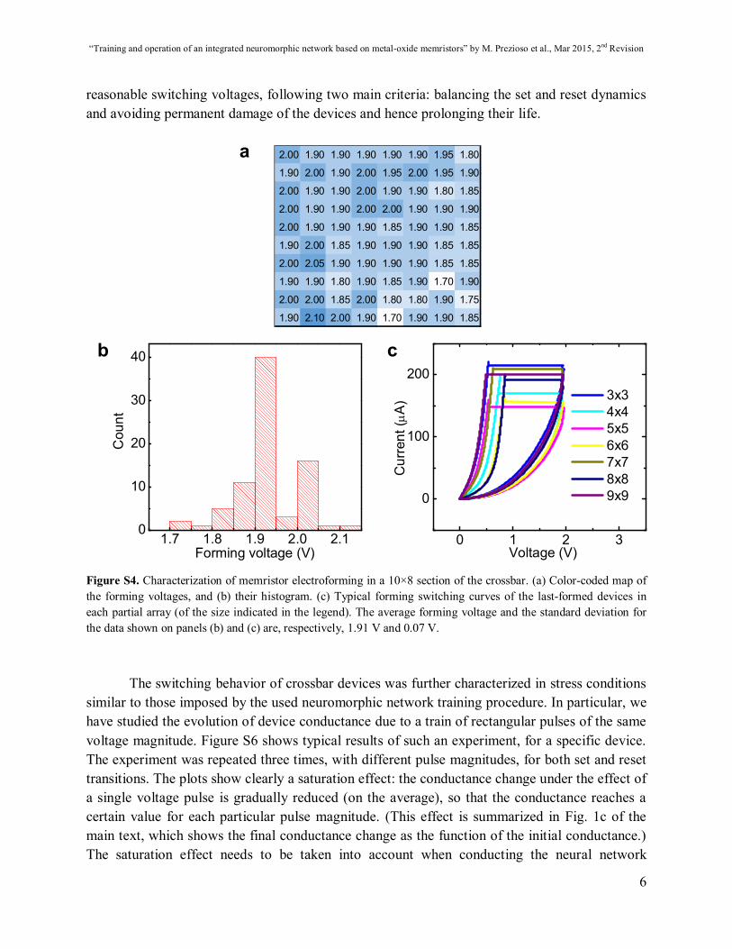
Specifically, we first characterized the “virgin” devices (not electroformed yet). Figures S3a and S3b show the recorded map of conductances measured at 0.1 V and the corresponding histogram, while Fig. S3c shows a representative set of dc I-V curves. After this characterization, the electroforming procedure was performed. For the forming, a quasi-DC current ramp was applied to the selected column line, while the selected row line was grounded and all the remaining (unselected) lines were kept floating. Such fixed-current technique prevents devices from an excessive stress during its electroforming, when device’s resistance drops sharply. To minimize the current leakage during forming, the already formed devices were switched to their low-conductive state. More particularly, the devices of a 2×2 subarray were formed first. Then the devices in additional rows and columns were formed, so that the subarray of formed devices was gradually increased: first to 3×3 devices, then to 4×4, and so on. Figure S4a shows the map of forming voltages for the working section of the crossbar, while Fig. S4b shows the corresponding histogram. Additionally, Figure S4c shows the electroforming process dynamics (for the diagonal devices, which were formed last to complete forming of the corresponding subarray) on the [I, V] plane.
Following the electroforming procedure, we characterized the effective switching thresholds for all devices in the working section of the crossbar array (Fig. S5). The threshold set / reset voltages were measured by first programming devices to their high / low resistive states, and then applying a sequence of 500-μs pulses of the appropriate polarity with gradually increasing amplitude to measure the smallest voltage that caused a resistance change by more than 2 kΩ. The evolution of device conductance during the reset and set switching are shown in Figs. S5a and S5b, respectively, while Figs. S5c and S5d show maps of the corresponding

“Training and operation of an integrated neuromorphic network based on metal-oxide memristors” by M. Prezioso et al., Mar 2015, 2nd Revision
5
effective reset and set threshold voltages. Panel (e) of Fig. S5 exhibits the data from its panels (c) and (d) in the form of histograms. The devices marked with ‘X’ in the threshold maps could not be switched with largest applied voltages.
5.5E-07 3.7E-07 4.2E-07 3.5E-07 5.0E-07 4.7E-07 4.4E-07 5.0E-07
3.7E-07 3.6E-07 6.3E-07 3.7E-07 4.1E-07 4.2E-07 5.3E-07 3.3E-07
4.6E-07 5.7E-07 5.4E-07 4.9E-07 4.9E-07 4.2E-07 5.6E-07 6.0E-07
4.6E-07 4.2E-07 3.6E-07 3.1E-07 2.7E-07 3.7E-07 4.4E-07 3.7E-07
3.5E-07 4.0E-07 5.8E-07 4.8E-07 6.5E-07 4.1E-07 4.0E-07 4.4E-07
4.5E-07 3.8E-07 5.4E-07 4.7E-07 5.9E-07 4.6E-07 4.7E-07 4.8E-07
3.6E-07 4.1E-07 4.5E-07 3.9E-07 5.0E-07 3.6E-07 5.6E-07 4.8E-07
3.5E-07 4.0E-07 4.3E-07 4.1E-07 3.5E-07 4.4E-07 4.6E-07 3.7E-07
4.9E-07 3.7E-07 6.0E-07 3.6E-07 3.3E-07 5.1E-07 3.9E-07 4.2E-07
4.4E-07 3.3E-07 3.3E-07 4.0E-07 3.9E-07 4.5E-07 4.3E-07 4.4E-07
cb
a
0.3 0.4 0.5 0.60
5
10
15
Cou
nts
Conductance @0.1V (S)-1.0 -0.5 0.0 0.5 1.0
-2
0
2
4 dev1 dev2 dev3 dev4
Cur
rent
(A
)
Voltage (V)
Figure S3. Pre-formed (virgin sample) characterization of a 10×8 section of the crossbar: (a) color-coded conductance map of device conductances measured at 0.1 V, (b) the corresponding histogram, and (c) dc I-V curves of four representative devices. The average conductance and the standard deviation of conductances represented in panels (b) and (c) are 0.43 S and 0.08 S, correspondingly.
Of these data, the fact most important for applications is that the spread in effective switching voltages is narrow enough to avoid the infamous half-select problem.6 For example, application of voltage +1.4 V to any device (besides those marked with X) ensures its set adjustment, while the half of that voltage (i.e. +0.7 V) is below the smallest observed set threshold voltage. This fact prevents disturbance of half-selected devices, connected to just one of voltage-biased lines. The switching threshold data were also important to identify a range of
“Training and operation of an integrated neuromorphic network based on metal-oxide memristors” by M. Prezioso et al., Mar 2015, 2nd Revision
6
reasonable switching voltages, following two main criteria: balancing the set and reset dynamics and avoiding permanent damage of the devices and hence prolonging their life.
0 1 2 3
0
100
200 3x3 4x4 5x5 6x6 7x7 8x8 9x9
Cur
rent
(A
)
Voltage (V)1.7 1.8 1.9 2.0 2.1
0
10
20
30
40
Cou
nt
Forming voltage (V)
2.00 1.90 1.90 1.90 1.90 1.90 1.95 1.80
1.90 2.00 1.90 2.00 1.95 2.00 1.95 1.90
2.00 1.90 1.90 2.00 1.90 1.90 1.80 1.85
2.00 1.90 1.90 2.00 2.00 1.90 1.90 1.90
2.00 1.90 1.90 1.90 1.85 1.90 1.90 1.85
1.90 2.00 1.85 1.90 1.90 1.90 1.85 1.85
2.00 2.05 1.90 1.90 1.90 1.90 1.85 1.85
1.90 1.90 1.80 1.90 1.85 1.90 1.70 1.90
2.00 2.00 1.85 2.00 1.80 1.80 1.90 1.75
1.90 2.10 2.00 1.90 1.70 1.90 1.90 1.85
a
cb
Figure S4. Characterization of memristor electroforming in a 10×8 section of the crossbar. (a) Color-coded map of the forming voltages, and (b) their histogram. (c) Typical forming switching curves of the last-formed devices in each partial array (of the size indicated in the legend). The average forming voltage and the standard deviation for the data shown on panels (b) and (c) are, respectively, 1.91 V and 0.07 V.
The switching behavior of crossbar devices was further characterized in stress conditions similar to those imposed by the used neuromorphic network training procedure. In particular, we have studied the evolution of device conductance due to a train of rectangular pulses of the same voltage magnitude. Figure S6 shows typical results of such an experiment, for a specific device. The experiment was repeated three times, with different pulse magnitudes, for both set and reset transitions. The plots show clearly a saturation effect: the conductance change under the effect of a single voltage pulse is gradually reduced (on the average), so that the conductance reaches a certain value for each particular pulse magnitude. (This effect is summarized in Fig. 1c of the main text, which shows the final conductance change as the function of the initial conductance.) The saturation effect needs to be taken into account when conducting the neural network

“Training and operation of an integrated neuromorphic network based on metal-oxide memristors” by M. Prezioso et al., Mar 2015, 2nd Revision
7
experiment: as stated in the main text, it is much better, in the beginning of network training, to initialize devices in the middle of their dynamical range, to achieve substantial conductance changes in the beginning of the training process.
-1.14 -1.42 -1.39 -1.20 -1.40 -1.09 -1.29 -1.08
-1.26 -1.26 -1.22 -0.84 -1.26 -0.80 -1.28 -1.25
-1.19 -1.04 -1.30 -1.14 -1.01 -1.20 -1.16 -1.12
-1.13 -1.25 -1.30 -1.15 -1.31 -1.04 -0.85 -1.17
-1.20 -1.07 -1.34 -0.99 -0.96 -1.24 -1.21 -1.14
-1.31 x x -1.14 -1.25 -1.27 -1.28 -1.24
-1.16 -1.26 -1.21 -1.27 -1.20 -1.23 -1.10 -1.18
-1.24 -1.11 -1.25 -1.20 -1.08 -1.28 -1.16 -1.16
-1.19 -1.12 -1.28 -1.28 -1.10 -1.29 -1.28 -1.26
x -1.05 -1.23 -0.90 -1.06 -1.17 -0.94 -1.26
0.98 1.04 1.06 0.81 1.01 1.01 0.81 0.95
0.82 1.08 0.96 0.85 1.15 0.81 1.06 0.80
1.07 0.94 0.80 1.02 0.96 0.84 0.91 0.91
0.82 0.83 1.00 0.82 1.00 0.99 0.87 1.07
0.84 1.00 0.96 1.00 0.88 0.84 1.06 1.06
1.04 x x 0.94 1.00 1.21 0.82 1.11
0.84 1.04 1.05 0.95 1.02 0.91 0.98 1.12
1.04 1.06 1.00 1.01 1.01 1.12 0.94 1.06
1.06 0.94 0.91 1.11 0.88 1.04 0.98 1.08
x 1.02 0.80 1.06 0.99 1.13 0.92 0.99
0.8 1 1.2 1.4 1.6 1.8
20
30
40
50
60
Voltage (V)
Con
duct
ance
(S
)
-1.8 -1.6 -1.4 -1.2 -1 -0.8
20
30
40
50
60
Voltage (V)
Con
duct
ance
(S
)
a b
c d
e
Cou
nt
Threshold voltage (V)
Figure S5. Characterization of the set and reset thresholds of formed memristors: (a, b) device conductance dynamics under applied voltage ramps of opposite polarities; (c, d) the effective threshold voltage maps for set and reset transitions, and (e) their histograms. The histograms on panel (e) do not include the 3 devices that could not be switched to the OFF state with voltages above -1.5 V; these devices are marked with crosses on panels (c) and (d). The average effective set/reset switching threshold voltages and their standard deviations, for the data shown on panel (e) are, respectively 0.9 V/-1.17 V and 0.1 V/0.12 V.

“Training and operation of an integrated neuromorphic network based on metal-oxide memristors” by M. Prezioso et al., Mar 2015, 2nd Revision
8
0 100 200 300 400 5000
20
40
60
80
100 -1.1V -1.2V -1.3V
Con
duct
ance
(S)
Pulse #
a
0 100 200 300 400 5000
20
40
60
80
100
Con
duct
ance
(S)
Pulse #
1.1V 1.2V 1.3V
b
Figure S6. Evolution of memristor's conductance (measured at 0.1 V) under the effect of 500-μs pulse trains of several magnitudes, for the (a) reset and (b) set switching. Note that unlike Figures S5a and S5b, this figure shows the change in conductance for a fixed-magnitude pulses applied repeatedly to the same device. The dashed lines are just guides for the eye.
5. Network training result analysis
The key metric of neural network classifier training is the difference it creates between network outputs induced by input patterns belonging to different classes. Two panels of Figure S7a show such difference for our memristor crossbar network. Namely, these are the histograms of the differences between currents in the “correct” and “incorrect” outputs for each of 30 input patterns. (Evidently, there are 60 such differences: for each of 30 inputs in 3 classes, there is one correct output and two incorrect ones.) In a perfectly trained classifier, all these differences have to be positive. The top panel shows that before training, the differences are small, and have random signs. During the training the differences increased, so that, as the lower panel shows, after a sufficient number (in this particular case, 21) of training epochs, all of them have become positive, signaling the 100% classification fidelity.
Figure S7b shows another useful way of understanding network dynamics during its training, namely the distributions of conductances at three phases of training process. (Note that the same information, but for only two phases, is presented in the inset of Fig. 4a of the main text.) For convenience, Fig. S7c shows the distributions of the effective weights W, i.e. the differences between the conductances of devices that form each differential pair, for the same three phases of training. As the data show, the difference of the weight distributions created by the training is less dramatic than that of the output signals, shown in panel (a), i.e. the training imposes mostly relative weight changes (which are important for the correct classification), rather than their global change.

“Training and operation of an integrated neuromorphic network based on metal-oxide memristors” by M. Prezioso et al., Mar 2015, 2nd Revision
9
20 40 60 8002468
10121416
Cou
nt
Device conductance, G (S)
Initial state Epoch 21 Epoch 54
b
-40 -20 0 20 400123456789
Cou
nt
Weight, W (S)
Initial state Epoch 21 Epoch 54
c
0 5 10 15 20 25
12345
C
ount
Icorrect-Iincorrect (A)
Epoch 21
1234567
Cou
nt
Class 1 'z' Class 2 'v' Class 3 'n'
Initial statea
Figure S7. Additional data from a particular pattern classification experiment (“Run 1”) for which the perfect classification has been achieved, for the first time, after 21 training epochs. (a) Histogram of differences between currents in the “correct” output (corresponding to input pattern’s class) and other two channels. (b) Histogram of device conductances at the initial state, measured after training epoch 21, and after epoch 54 (for which classification is also perfect). (c) Histogram of the differential weights W defined by Eq. (3) of main text. In panel (b), the average values / standard deviations of the measured conductances are 36.3 μS / 9 μS, 41.9 μS / 13 μS, and 42.4 μS / 13.4 μS, when measured in the initial state, after epoch 21, and epoch 54, respectively. The corresponding averages / deviations of the weights in panel (c) are -0.24 μS / 2.83μS, -5.36 μS / 16.8 μS, and -1.17 μS / 17.1 μS.
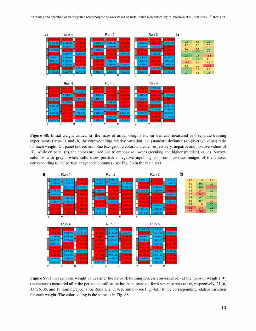
Finally, Figures S8 and S9 show the weight maps measured before and after training for 6 separate training experiments (“runs”). (The convergence graphs for these experiments are shown in Fig. 4a of the main text). The comparison of weight maps in Fig. S8 shows that even though the initialization procedure was similar in all runs, there were some run-to-run variations of the state of same device. (To quantify the variations, Figs. S8b and S9b show relative standard deviations for each of 30 weights.)
“Training and operation of an integrated neuromorphic network based on metal-oxide memristors” by M. Prezioso et al., Mar 2015, 2nd Revision
10
-1.62E-06 -1.30E-06 -1.78E-06
3.75E-06 2.52E-06 -4.46E-06
-2.36E-06 6.50E-07 -6.15E-06
2.87E-06 -2.41E-06 -3.00E-07
-4.73E-06 3.30E-07 1.93E-06
7.50E-07 1.59E-06 -6.23E-068.60E-07 4.16E-06 -2.80E-07
-2.85E-07 1.72E-06 -3.18E-06
-8.85E-07 -1.65E-06 2.65E-07
5.19E-06 1.60E-06 2.24E-06
-3.98E-06 -1.22E-06 -1.66E-06
1.42E-06 1.50E-07 -7.87E-06
-3.10E-06 6.49E-08 -6.25E-06
1.97E-06 -4.31E-06 -3.41E-06
-5.35E-06 -1.49E-08 1.49E-06
3.31E-06 -5.65E-07 -9.75E-06-9.75E-07 3.16E-06 -1.37E-06
-5.45E-07 1.46E-06 7.00E-08
-1.35E-06 -3.65E-07 -3.80E-07
1.36E-05 3.69E-06 1.12E-06
-2.57E-06 -1.61E-06 -3.35E-06
3.01E-06 -3.95E-06 4.82E-06
2.70E-07 1.62E-06 -2.30E-07
-6.55E-07 -3.87E-06 -2.11E-06
-5.46E-06 3.12E-06 -1.20E-07
4.60E-07 -4.89E-05 6.10E-071.33E-06 -3.25E-06 4.26E-06
3.20E-07 -1.70E-06 1.09E-06
-5.51E-08 2.95E-06 -3.77E-06
5.50E-06 -5.87E-06 1.33E-06
-2.35E-07 -5.67E-06 -2.38E-06
-1.05E-07 -4.06E-06 7.04E-06
-1.20E-07 5.15E-07 -1.96E-06
3.16E-06 -7.09E-06 9.50E-08-4.36E-06 2.78E-06 -1.44E-06
1.39E-06 -4.91E-05 -1.15E-06
7.15E-07 -1.20E-06 3.01E-061.42E-06 -2.43E-06 1.16E-06
-9.95E-07 -1.30E-06 -9.65E-07
4.37E-06 -4.78E-06 1.33E-06
-9.15E-07 -1.13E-06 -7.15E-06
-3.26E-06 -1.85E-06 -3.50E-06
1.63E-06 -2.60E-06 -2.66E-06
1.26E-06 -5.10E-07 -4.58E-06-6.36E-06 4.19E-06 -5.80E-07
-6.92E-06 -4.61E-05 -5.60E-07
0.00E+00 3.50E-07 2.68E-063.61E-06 -2.52E-06 8.00E-08
-1.24E-06 1.27E-06 -1.44E-06
6.56E-06 -5.67E-06 1.12E-06
-4.06E-06 4.10E-07 -5.77E-06
-1.74E-06 -7.60E-06 -1.41E-06
1.17E-06 -2.28E-06 1.51E-08
4.98E-06 -5.17E-06 -1.38E-06-4.55E-06 4.91E-06 -1.96E-06
-1.28E-05 -4.60E-05 5.50E-08
-1.36E-06 1.23E-06 2.18E-068.50E-07 -1.41E-06 3.55E-07
-1.42E-06 -2.77E-06 1.77E-06
1.12E-05 -3.66E-06 -6.35E-07
Run 1 Run 2 Run 3
Run 6Run 5Run 4
0.6 1.1 0.64.8 1.3 5.84.2 4.6 0.90.8 0.5 0.80.1 0.7 12.32.5 0.7 1.310.1 3.4 1.11.5 2.2 21.10.5 6.2 2.20.4 1.5 0.8
a b
z v n z v n z v n
z v n z v n z v n
Figure S8: Initial weight values: (a) the maps of initial weights Wij (in siemens) measured in 6 separate training experiments (“runs”), and (b) the corresponding relative variation, i.e. (standard deviation)-to-(average value) ratio for each weight. On panel (a), red and blue background colors indicate, respectively, negative and positive values of Wij, while on panel (b), the colors are used just to emphasize lower (greenish) and higher (reddish) values. Narrow columns with gray / white cells show positive / negative input signals from noiseless images of the classes corresponding to the particular synaptic columns - see Fig. 3b in the main text.
1.7 1.6 1.81.0 0.6 0.71.1 0.6 5.80.9 2.7 0.62.7 5.1 0.80.8 0.7 0.51.0 0.7 2.50.8 1.6 0.36.0 3.4 0.33.7 5.9 0.6
9.72E-06 1.61E-05 -4.48E-055.65E-06 2.32E-05 -2.08E-06
-6.41E-06 6.31E-06 3.12E-052.02E-05 -6.32E-06 -9.09E-06
1.96E-06 -9.87E-06 -2.93E-05-3.96E-06 1.56E-06 -1.18E-05
9.85E-07 4.09E-06 -2.91E-05-5.28E-06 -1.65E-05 -1.38E-05
-6.55E-07 -3.55E-05 -1.49E-05-2.63E-06 -1.33E-05 -2.64E-05
5.84E-06 8.16E-06 -2.48E-052.40E-07 1.24E-05 1.10E-05
-3.29E-06 -2.85E-07 2.54E-051.06E-05 -1.44E-05 -6.10E-07
-5.11E-06 -2.07E-06 -5.95E-06
1.74E-06 -2.76E-06 -1.58E-05-1.93E-06 4.44E-06 -2.69E-05
-2.77E-06 -5.96E-06 -1.44E-051.21E-06 -2.95E-05 -2.80E-05
2.78E-06 -1.54E-05 -3.13E-05
6.89E-06 -6.34E-06 1.93E-05-7.47E-06 -2.06E-06 1.39E-05
-1.57E-05 1.69E-06 -1.05E-069.32E-06 7.05E-07 -1.97E-05
-5.17E-06 -1.02E-06 5.95E-07
-1.59E-06 -4.19E-05 -6.25E-06-2.38E-06 -1.66E-06 4.29E-06
-4.42E-06 1.21E-05 -1.57E-051.50E-07 2.88E-05 -3.44E-05
5.61E-06 2.32E-06 -7.50E-06
-5.66E-06 -4.15E-06 1.39E-06-1.73E-05 1.35E-05 5.78E-06
1.12E-06 7.05E-06 -9.03E-066.34E-06 1.28E-05 -1.58E-05
9.08E-06 -1.84E-06 -7.69E-06
-9.35E-06 -4.30E-05 -3.99E-06-5.02E-06 7.84E-06 3.38E-06
-6.58E-06 1.49E-05 -1.32E-053.59E-06 2.41E-05 -2.90E-05
2.40E-06 -7.90E-07 -7.01E-06
2.58E-06 1.18E-05 -4.17E-06-2.12E-05 1.37E-05 1.03E-05
3.60E-07 7.45E-06 -1.31E-053.11E-06 1.42E-05 -2.78E-05
-7.16E-06 1.02E-05 -1.00E-05
-7.39E-06 -4.25E-05 -1.09E-05-1.34E-05 1.23E-05 2.06E-06
-2.52E-05 3.44E-05 -2.60E-051.31E-06 3.66E-05 -3.89E-05
-7.14E-06 1.46E-05 -2.48E-05
-1.00E-06 5.02E-06 -1.59E-05-2.74E-05 8.73E-06 2.03E-05
-2.05E-05 6.95E-06 -1.43E-05-3.27E-06 2.02E-05 -2.78E-05
-6.52E-06 1.41E-05 -1.44E-05
-8.91E-06 -4.56E-05 -3.92E-06-1.63E-05 8.44E-06 8.70E-06
-2.11E-05 2.60E-05 -2.29E-05-3.46E-06 2.69E-05 -3.39E-05
6.93E-06 2.26E-06 -4.97E-06
Run 1 Run 2 Run 3
Run 6Run 5Run 4
z v n z v n z v n
z v n z v n z v n
a b
Figure S9: Final synaptic weight values after the network training process convergence: (a) the maps of weights Wij (in siemens) measured after the perfect classification has been reached, for 6 separate runs (after, respectively, 21, 6, 33, 26, 35, and 18 training epochs for Runs 1, 2, 3, 4, 5, and 6 – see Fig. 4a); (b) the corresponding relative variation for each weight. The color coding is the same as in Fig. S8.

“Training and operation of an integrated neuromorphic network based on metal-oxide memristors” by M. Prezioso et al., Mar 2015, 2nd Revision
11
As Fig. S9 shows, after training the weights become markedly different - not only in their magnitude, but in many cases also in their sign, despite the fact that each final distribution provides perfect classification fidelity. This is in agreement with the well-known fact that the classifier training using the Delta Rule algorithm and its cousins (such as the Manhattan Update Rule used in this work) does not result in a unique synaptic weight distribution – unless the initial weight values are exactly the same in each training run.
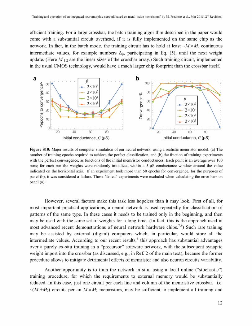
6. Computer simulations
We have also carried out extensive computer simulations of our neural network, in order to understand the impact of various parameters, most importantly of the initial device conductances, on classifier’s fidelity and convergence speed. To perform the simulation, an approximate device model was derived from the data shown on Fig. 1c of the main text. In this model, the conductance increase (ΔGset) by a positive voltage pulse and its decrease (ΔGreset) by the negative pulse are calculated as
ΔGset(G) = +10-3(106G – 106Gmin + 10 vset / slope ) –slope , (S1)
ΔGreset(G) = - 10-3(-106G + 106Gmax + 10 vreset / slope ) –slope , (S2)
where constant slope, for our specific pulse amplitude and duration was taken equal to 2, while parameters vset and vreset were randomly chosen from the range [1, 5.5] for every memristor before each run. Constants Gmin = 10 μS and Gmax = 100 μS are the minimum and maximum conductance values; G is always clipped between these values after each update. Such simple model captures two main features of the memristors, namely the saturation of the switching dynamics (Fig. 1c) and switching threshold variations (Fig. S5).
Fig. S10 shows the most important results of these simulations. First, they have confirmed that the classifier fidelity and convergence speed are the best when the initial conductances of the devices are in the middle of their dynamical range. The second important simulation result is that the performance is rather insensitive to the choice of parameter β, with the optimal value close to β = 2×10⁵. As was stated in the main text, these results had been used at network training.
7. Toward practical applications
We believe that our work is the first proof-of-concept that passively integrated memristive crossbar circuits can be used to perform classification task. However, due to its small size, this network is not by itself practical, and several major steps have to be made toward larger, useful neuromorphic networks.
Besides the primary, self-evident task of fabrication much larger crossbars with smaller memristors of (at least) similar quality and reproducibility, there is also a challenge of their
“Training and operation of an integrated neuromorphic network based on metal-oxide memristors” by M. Prezioso et al., Mar 2015, 2nd Revision
12
efficient training. For a large crossbar, the batch training algorithm described in the paper would come with a substantial circuit overhead, if it is fully implemented on the same chip as the network. In fact, in the batch mode, the training circuit has to hold at least ~M1M2 continuous intermediate values, for example numbers ij, participating in Eq. (5), until the next weight update. (Here M 1,2 are the linear sizes of the crossbar array.) Such training circuit, implemented in the usual CMOS technology, would have a much larger chip footprint than the crossbar itself.
20 40 60 800
10
20
30
40
50
initial state
epoc
hsto
conv
erge
nce
20 40 60 800
20
40
60
80
100
initial stateCo
nver
genc
e,5
0ep
ochs
Initial conductance, G (μS)
<epo
chs
to c
onve
rgen
ce>
Conv
erge
nce
%
Initial conductance, G (μS)
a b
rf 0.2rf 0.02rf 0.002rf 0.0002
β2×10⁶
2×10⁵
2×10⁴
2×10³
rf 0.2rf 0.02rf 0.002rf 0.0002
β2×10⁶
2×10⁵
2×10⁴
2×10³
Figure S10: Major results of computer simulation of our neural network, using a realistic memristor model. (a) The number of training epochs required to achieve the perfect classification, and (b) the fraction of training experiments with the perfect convergence, as functions of the initial memristor conductances. Each point is an average over 100 runs; for each run the weights were randomly initialized within a 5-μS conductance window around the value indicated on the horizontal axis. If an experiment took more than 50 epochs for convergence, for the purposes of panel (b), it was considered a failure. These "failed" experiments were excluded when calculating the error bars on panel (a).
However, several factors make this task less hopeless than it may look. First of all, for most important practical applications, a neural network is used repeatedly for classification of patterns of the same type. In these cases it needs to be trained only in the beginning, and then may be used with the same set of weights for a long time. (In fact, this is the approach used in most advanced recent demonstrations of neural network hardware chips.7,8) Such rare training may be assisted by external (digital) computers which, in particular, would store all the intermediate values. According to our recent results,9 this approach has substantial advantages over a purely ex-situ training in a “precursor” software network, with the subsequent synaptic weight import into the crossbar (as discussed, e.g., in Ref. 2 of the main text), because the former procedure allows to mitigate detrimental effects of memristor and also neuron circuits variability.
Another opportunity is to train the network in situ, using a local online (“stochastic”) training procedure, for which the requirements to external memory would be substantially reduced. In this case, just one circuit per each line and column of the memristive crossbar, i.e. ~(M1+M2) circuits per an M1M2 memristors, may be sufficient to implement all training and

“Training and operation of an integrated neuromorphic network based on metal-oxide memristors” by M. Prezioso et al., Mar 2015, 2nd Revision
13
neuron functions. As the crossbar is scaled up in future for more complex tasks (up to M1.2 ~103-104 deemed necessary for some cognitive architectures), the relative size of this circuit overhead would be much decreased. Figure S11 shows some results of our preliminary attempt at implementing online training algorithm using the same memristive crossbar. Perfect classification has been achieved for the used small set of input patterns, but unfortunately, in its current form the online learning requires too many synaptic updates to achieve the perfect network performance.
Another important question which must be addressed in practical application is the generalization performance of the classifier. As Fig. S11 shows, for online training we could reach a perfect classification performance on a small separate test set. However, this training was too slow for our basic experiments with 30 images in 3 classes. As stated in the main text, these experiments were carried out without a separate test set, but using the measured values of weights recorded after every training epoch, we could use computer simulations to estimate network's generalization ability, i.e. its possible classification performance on a separate test set (not used at training). The set consisted of all possible patterns (36 patterns in each of 3 classes) obtained from the ideal images (Fig. 2c of main text) by flipping 2 pixels – see Fig. S12b. Though the classification improved during training (Fig. S12a), typically it is not perfect by its end. This is not surprising, giving the fact that the minimum Hamming distances between patterns of the test and training sets are 2 and 4, accordingly. Indeed, even a human would hardly be able to classify all these patterns correctly – please have one more look at Fig. S12b.
Training set Test set
0 50 100 150 200 250
0
2
4
6
8
10
12 Training set Test set
# m
issc
lass
ified
pat
tern
s
Iteration #
a b
x
i
cv
Figure S11: Preliminary results for pattern classification experiment using online ("stochastic") Manhattan Rule training: (a) Classification convergence for the training and test sets, and (b) used sets. On panel (a), "iteration" means an application of one pattern from a training set, followed by the corresponding weight update. (There were 12 iterations in training epoch.) Note that here perfect classification was achieved on the (admittedly, extremely small) test set. (The evaluation on this set was performed only at the end of training.)

“Training and operation of an integrated neuromorphic network based on metal-oxide memristors” by M. Prezioso et al., Mar 2015, 2nd Revision
14
As a result, we believe that a convincing demonstration of the generalization ability is only possible on larger input vectors, which in turn require larger networks (and hence larger crossbar arrays). Such a demonstration remains one of our major future goals.
z
v
n
a b
020406080
100
0 10 20 30 40 5005
1015202530
Test set
26% misclassification
# m
iscl
assi
fied
patte
rns
Training set
Epoch
Figure S12: Pattern classification experiment (Run 1): (a) Classification convergence for the training and test sets, and (b) the used test set. (The training set and the training method were the same as described in main text). The bottom figure on panel (a) shows one of the curves (black one) from Fig. 4a, extended to the subsequent training epochs.
References
1. Young-Fisher, K. G. et al. Leakage current-forming voltage relation and oxygen gettering in HfOx RRAM devices. IEEE Electron Device Lett. 34, 750–752 (2013).
2. Yang, J. J. et al. The mechanism of electroforming of metal oxide memristive switches. Nanotechnology 20, 215201 (2009).
3. Lentz, F. et al. Current compliance-dependent nonlinearity in TiO2 RRAM. IEEE Electron Device Lett. 34, 996–998 (2013).
4. Goux, L. et al. Ultralow sub-500nA operating current high-performance TiN/Al2O3/HfO2 /Hf/TiN bipolar RRAM achieved through understanding-based stack-engineering. VLSI Symp. Technol.’12, 159–160 (2012).
5. Wu, H. et al. Resistive switching performance improvement of Ta2O5-x/TaOy bilayer ReRAM devices by inserting AlOδ barrier layer. IEEE Electron Device Lett. 35, 39–41 (2014).
6. Strukov, D. B., Likharev, K. K. Reconfigurable nano-crossbar architectures. Nanoelectronics and Information Technology, Waser, R. (ed.), 3rd ed. (Wiley, Weinheim, Germany, 2012).
7. Merolla, P. A. et al. A million spiking-neuron integrated circuit with a scalable communication network and interface. Science 345, 668-673 (2014).

“Training and operation of an integrated neuromorphic network based on metal-oxide memristors” by M. Prezioso et al., Mar 2015, 2nd Revision
15
8. Farabet, C. et al. NeuFlow: A runtime reconfigurable dataflow processor for vision. CVPRW’11, 109-116 (2011).
9. Kataeva, I. et al. Efficient training algorithms for neural networks based on memristive crossbar circuits. submitted to IJCNN’15, (2015), available online at https://www.ece.ucsb.edu/~strukov/papers/2015/mlpclassifier.pdf .