monte carlo simulation of charge transport in organic solar cells
TRANSCRIPT

DEPARTMENT OF ELECTRICAL AND COMPUTER ENGINEERING DUKE UNIVERSITY
Monte Carlo Simulation of Charge Transport in Organic
Solar Cells Undergraduate Thesis
Xin Xu Advisor: Associate Professor Adrienne D. Stiff-Roberts
4/18/2012

Contents
Abstract ....................................................................................................................................................................................... 2
Introduction ............................................................................................................................................................................... 2
The Organic Solar Cell ....................................................................................................................................................... 2
Photovoltaic Process ......................................................................................................................................................... 4
Literature Review ............................................................................................................................................................... 5
Motivation .................................................................................................................................................................................. 6
Model Description ................................................................................................................................................................... 6
Bulk Heterojunction Morphology Generator .......................................................................................................... 6
Exciton Generation Rate .................................................................................................................................................. 8
Charge Transport Model ................................................................................................................................................ 13
Results ........................................................................................................................................................................................ 16
Morphology ......................................................................................................................................................................... 16
Exciton Generation Rate ................................................................................................................................................ 18
Charge Transport Model ................................................................................................................................................ 21
Discussion ................................................................................................................................................................................. 22
Conclusions and Future Work .......................................................................................................................................... 23
Acknowledgements .............................................................................................................................................................. 24

Abstract
Organic solar cells have advantages over the traditional inorganic solar cells. The flexibility
and light-weight of an organic solar device lead to novel deployment unattainable by inorganic
solar devices. There is a wide range of materials that can be used to fabricate an organic solar cell
with many suitable conducting polymers and small molecules. The large number of appropriate
materials means that it is possible to tune an organic cell to target specific wavelengths of light by
targeting specific band gaps. Despite all these benefits, the commercialization of organic solar
devices has been limited by their low efficiency. One path to raising the efficiency is to better
understand how the morphology or internal structure of the solar cell influences charge transport.
The work presented here is a Dynamical Monte Carlo (DMC) simulation that can model the
processes that govern the conversion of light to electrical power. The Monte Carlo simulation
describes how the interacting particles in the solar cell move and behave. This simulation can
provide insight to how the structure of the cell can influence both charge creation and charge
collection. The DMC simulations were performed for two archetypal organic solar cell material
systems: CuPc-C60 and P3HT-PCBM. Various morphologies were used for these material systems
to examine the effect of morphology on both internal and external quantum efficiency.
Introduction
Since the introduction of the bilayer donor-acceptor heterojunction organic solar cell by
C.W. Tang in 1986 [1], organic solar cell efficiencies have been rising. However, the efficiencies of
organic photovoltaic (OPV) cells still lag behind their inorganic counterparts, with the most efficient
OPV cell rated at 10% efficiency [2]. The challenges to successful organic solar cell design are
numerous. Chief among these is that organic solar cell physics differs greatly from that of inorganic
solar cells. Thus, the theoretical framework developed to describe inorganic solar cells cannot be
directly applied to organics. A new approach for organic solar cells is needed.
The Organic Solar Cell
The physics and analysis of organic solar cells differ greatly from their inorganic
counterparts. The energy states are distributed differently in an organic vs. inorganic solar cell.
For an inorganic solar cell, the periodicity of the inorganic semiconductor crystal lattice leads to the
formation of conduction bands and valence bands. The charges move along these bands and carrier
movement can be solved analytically with Bloch wave functions [3]. Organic solar cells have two
important energy states: highest occupied molecular orbital (HOMO) and lowest unoccupied
molecular orbital (LUMO). Rather than form energy bands, the disorder of the organic cell leads to
highly localized states. Charge movement is described by hopping from localized state to localized
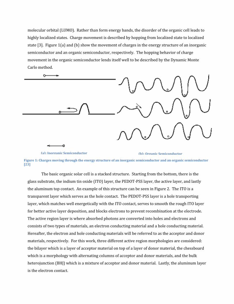
state [3]. Figure 1(a) and (b) show the movement of charges in the energy structure of an inorganic
semiconductor and an organic semiconductor, respectively. The hopping behavior of charge
movement in the organic semiconductor lends itself well to be described by the Dynamic Monte
Carlo method.
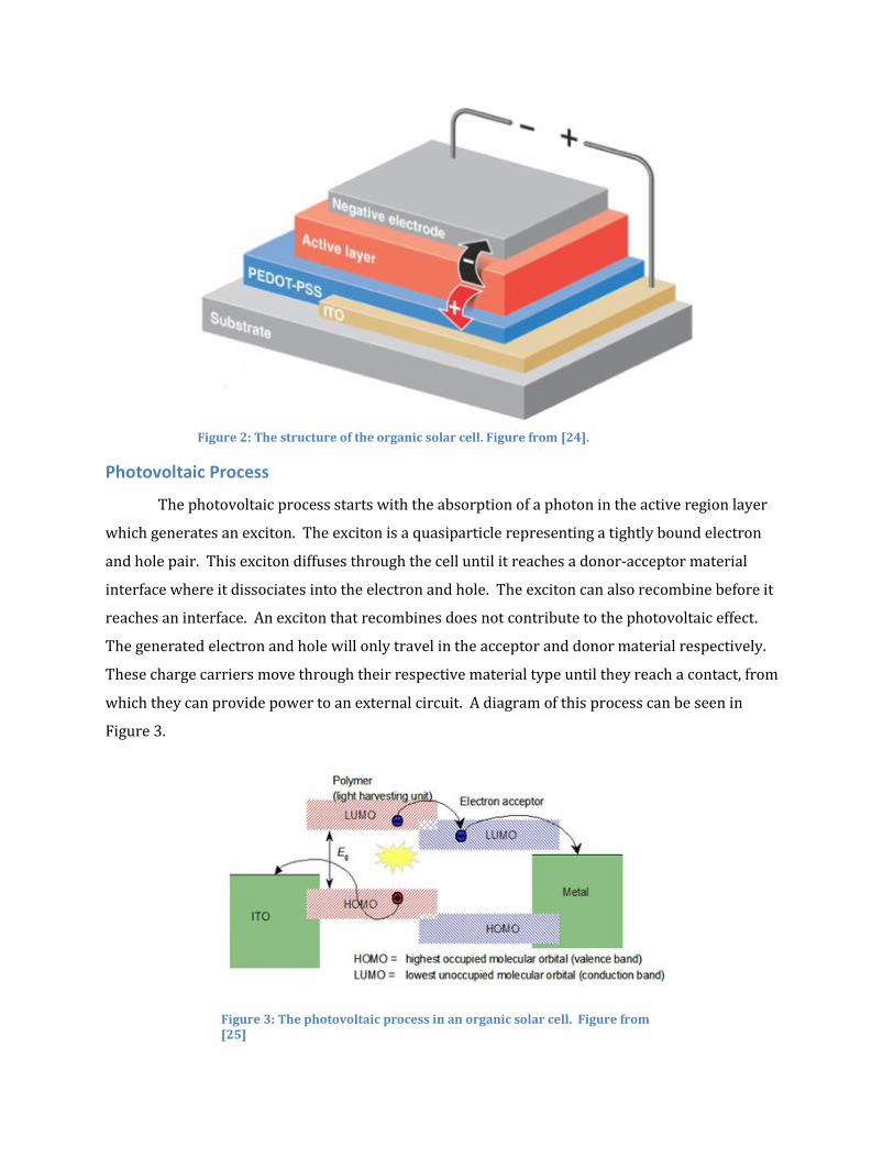
The basic organic solar cell is a stacked structure. Starting from the bottom, there is the
glass substrate, the indium tin oxide (ITO) layer, the PEDOT-PSS layer, the active layer, and lastly
the aluminum top contact. An example of this structure can be seen in Figure 2. The ITO is a
transparent layer which serves as the hole contact. The PEDOT-PSS layer is a hole transporting
layer, which matches well energetically with the ITO contact, serves to smooth the rough ITO layer
for better active layer deposition, and blocks electrons to prevent recombination at the electrode.
The active region layer is where absorbed photons are converted into holes and electrons and
consists of two types of materials, an electron conducting material and a hole conducting material.
Hereafter, the electron and hole conducting materials will be referred to as the acceptor and donor
materials, respectively. For this work, three different active region morphologies are considered:
the bilayer which is a layer of acceptor material on top of a layer of donor material, the chessboard
which is a morphology with alternating columns of acceptor and donor materials, and the bulk
heterojunction (BHJ) which is a mixture of acceptor and donor material. Lastly, the aluminum layer
is the electron contact.
Figure 1: Charges moving through the energy structure of an inorganic semiconductor and an organic semiconductor [23]
(a): Inorganic Semiconductor (b): Organic Semiconductor
Photovoltaic Process
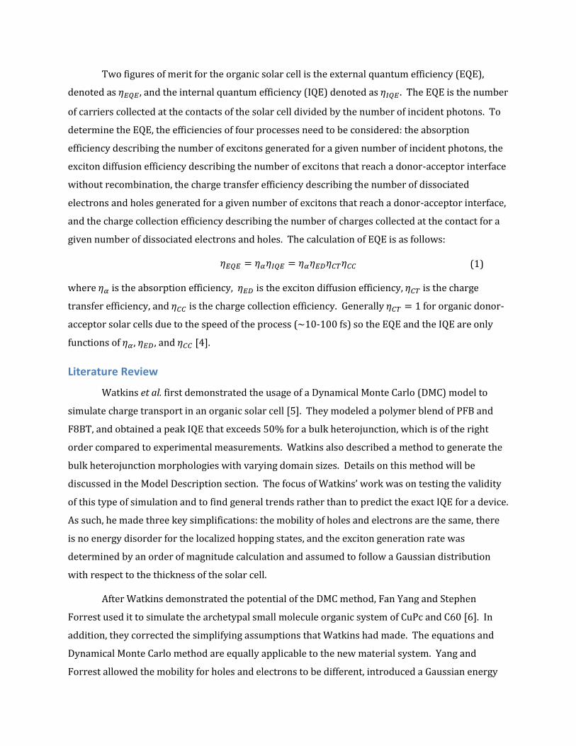
The photovoltaic process starts with the absorption of a photon in the active region layer
which generates an exciton. The exciton is a quasiparticle representing a tightly bound electron
and hole pair. This exciton diffuses through the cell until it reaches a donor-acceptor material
interface where it dissociates into the electron and hole. The exciton can also recombine before it
reaches an interface. An exciton that recombines does not contribute to the photovoltaic effect.
The generated electron and hole will only travel in the acceptor and donor material respectively.
These charge carriers move through their respective material type until they reach a contact, from
which they can provide power to an external circuit. A diagram of this process can be seen in
Figure 3.
Figure 2: The structure of the organic solar cell. Figure from [24].
Figure 3: The photovoltaic process in an organic solar cell. Figure from [25]
Two figures of merit for the organic solar cell is the external quantum efficiency (EQE),
denoted as , and the internal quantum efficiency (IQE) denoted as . The EQE is the number
of carriers collected at the contacts of the solar cell divided by the number of incident photons. To
determine the EQE, the efficiencies of four processes need to be considered: the absorption
efficiency describing the number of excitons generated for a given number of incident photons, the
exciton diffusion efficiency describing the number of excitons that reach a donor-acceptor interface
without recombination, the charge transfer efficiency describing the number of dissociated
electrons and holes generated for a given number of excitons that reach a donor-acceptor interface,
and the charge collection efficiency describing the number of charges collected at the contact for a
given number of dissociated electrons and holes. The calculation of EQE is as follows:
(1)
where is the absorption efficiency, is the exciton diffusion efficiency, is the charge
transfer efficiency, and is the charge collection efficiency. Generally for organic donor-
acceptor solar cells due to the speed of the process (~10-100 fs) so the EQE and the IQE are only
functions of , , and [4].
Literature Review
Watkins et al. first demonstrated the usage of a Dynamical Monte Carlo (DMC) model to
simulate charge transport in an organic solar cell [5]. They modeled a polymer blend of PFB and
F8BT, and obtained a peak IQE that exceeds 50% for a bulk heterojunction, which is of the right
order compared to experimental measurements. Watkins also described a method to generate the
bulk heterojunction morphologies with varying domain sizes. Details on this method will be
discussed in the Model Description section. The focus of Watkins’ work was on testing the validity
of this type of simulation and to find general trends rather than to predict the exact IQE for a device.
As such, he made three key simplifications: the mobility of holes and electrons are the same, there
is no energy disorder for the localized hopping states, and the exciton generation rate was
determined by an order of magnitude calculation and assumed to follow a Gaussian distribution
with respect to the thickness of the solar cell.
After Watkins demonstrated the potential of the DMC method, Fan Yang and Stephen
Forrest used it to simulate the archetypal small molecule organic system of CuPc and C60 [6]. In
addition, they corrected the simplifying assumptions that Watkins had made. The equations and
Dynamical Monte Carlo method are equally applicable to the new material system. Yang and
Forrest allowed the mobility for holes and electrons to be different, introduced a Gaussian energy
disorder for the localized states, and calculated the exciton generation rate by multiplying the
optical field intensity within the cell and with the material absorption coefficient of the cell. By
improving the accuracy of these components of the model, Yang and Forrest obtained simulated
EQEs very close to experimental measurements. For the bilayer morphology, the simulated EQE is
0.13 compared to a measured EQE of 0.14±0.1, and for the bulk heterojunction morphology the
simulated EQE is 0.16 compared to a measured EQE of 0.16±0.1.
Motivation
The motivation for this work comes from the Stiff-Roberts Lab’s need for an in house
simulation tool for organic solar cells. As opposed to the Yang and Forrest model for small
molecule solar cells of CuPc and C60, we are more focused on the bulk heterojunction solar cell
comprising of PCBM small molecules embedded in a P3HT polymer matrix. Additionally, we use a
unique deposition technique called matrix assisted pulsed laser evaporation (MAPLE) to build solar
cells. MAPLE gives more control of the morphology of the solar cell than other deposition
techniques like drop-casting or spin-casing. We wish to have a tool to model these morphologies.
By building a model more suited to our unique needs, we can save time, materials and costs by
predicting the performance of our solar cells before we build them.
Model Description
The model that was built as part of this thesis work consisted of three parts: a Metropolis
Algorithm Monte Carlo for the Ising Model to generate the bulk heterojunction morphologies, a
transfer matrix calculation from which an exciton generation rate and distribution is determined,
and a Dynamical Monte Carlo to simulate charge transport within the organic solar cell.
Bulk Heterojunction Morphology Generator
The first part of the model is the generation of the random bulk heterojunction (BHJ)
morphology. This is the same method as used by Watkins et al [5]. These BHJ morphologies were
generated using the Ising Model and Kawasaki spin dynamics governed by the Metropolis
Algorithm Monte Carlo. The method starts by assigning every lattice point or occupation site in our
organic solar cell a “spin” of “1” or “-1”, which corresponds to either a donor material or an acceptor
material. Our initial morphology is thus a completely disordered random state.
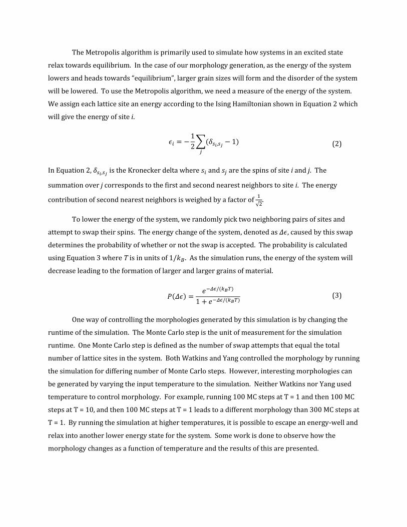
The Metropolis algorithm is primarily used to simulate how systems in an excited state
relax towards equilibrium. In the case of our morphology generation, as the energy of the system
lowers and heads towards “equilibrium”, larger grain sizes will form and the disorder of the system
will be lowered. To use the Metropolis algorithm, we need a measure of the energy of the system.
We assign each lattice site an energy according to the Ising Hamiltonian shown in Equation 2 which
will give the energy of site i.
∑
(2)
In Equation 2, is the Kronecker delta where and are the spins of site i and j. The
summation over j corresponds to the first and second nearest neighbors to site i. The energy
contribution of second nearest neighbors is weighed by a factor of
√ .
To lower the energy of the system, we randomly pick two neighboring pairs of sites and
attempt to swap their spins. The energy change of the system, denoted as , caused by this swap
determines the probability of whether or not the swap is accepted. The probability is calculated
using Equation 3 where T is in units of . As the simulation runs, the energy of the system will
decrease leading to the formation of larger and larger grains of material.
(3)
One way of controlling the morphologies generated by this simulation is by changing the
runtime of the simulation. The Monte Carlo step is the unit of measurement for the simulation
runtime. One Monte Carlo step is defined as the number of swap attempts that equal the total
number of lattice sites in the system. Both Watkins and Yang controlled the morphology by running
the simulation for differing number of Monte Carlo steps. However, interesting morphologies can
be generated by varying the input temperature to the simulation. Neither Watkins nor Yang used
temperature to control morphology. For example, running 100 MC steps at T = 1 and then 100 MC
steps at T = 10, and then 100 MC steps at T = 1 leads to a different morphology than 300 MC steps at
T = 1. By running the simulation at higher temperatures, it is possible to escape an energy-well and
relax into another lower energy state for the system. Some work is done to observe how the
morphology changes as a function of temperature and the results of this are presented.
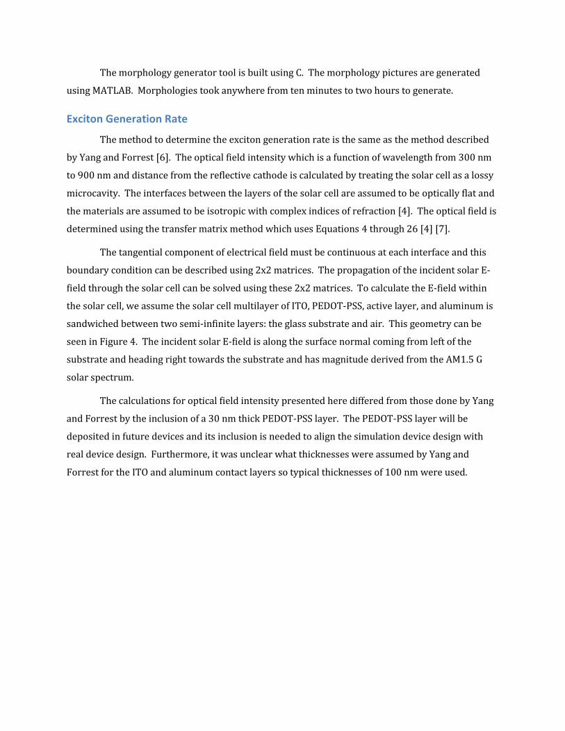
The morphology generator tool is built using C. The morphology pictures are generated
using MATLAB. Morphologies took anywhere from ten minutes to two hours to generate.
Exciton Generation Rate
The method to determine the exciton generation rate is the same as the method described
by Yang and Forrest [6]. The optical field intensity which is a function of wavelength from 300 nm
to 900 nm and distance from the reflective cathode is calculated by treating the solar cell as a lossy
microcavity. The interfaces between the layers of the solar cell are assumed to be optically flat and
the materials are assumed to be isotropic with complex indices of refraction [4]. The optical field is
determined using the transfer matrix method which uses Equations 4 through 26 [4] [7].
The tangential component of electrical field must be continuous at each interface and this
boundary condition can be described using 2x2 matrices. The propagation of the incident solar E-
field through the solar cell can be solved using these 2x2 matrices. To calculate the E-field within
the solar cell, we assume the solar cell multilayer of ITO, PEDOT-PSS, active layer, and aluminum is
sandwiched between two semi-infinite layers: the glass substrate and air. This geometry can be
seen in Figure 4. The incident solar E-field is along the surface normal coming from left of the
substrate and heading right towards the substrate and has magnitude derived from the AM1.5 G
solar spectrum.
The calculations for optical field intensity presented here differed from those done by Yang
and Forrest by the inclusion of a 30 nm thick PEDOT-PSS layer. The PEDOT-PSS layer will be
deposited in future devices and its inclusion is needed to align the simulation device design with
real device design. Furthermore, it was unclear what thicknesses were assumed by Yang and
Forrest for the ITO and aluminum contact layers so typical thicknesses of 100 nm were used.

At an interface between layer j and k, the propagation of the electric field is described by the
interface matrix , and as seen in Equation 4. The terms and that make up the interface
matrix are the complex valued Fresnel coefficients, where and are the complex indices of
refraction for layer j and k respectively.
[
] [
]
[
]
[
] (4)
(5)
(6)
Figure 4: Geometry used for the optical electrical field calculation. Layer 0 and m+1 are the glass substrate and air respectively.

There is the propagation matrix which describes the absorption and phase shift of the E-
field within layer j. Here is the complex index of refraction of layer j and is the wavelength in
vacuum.
[
] (7)
(
) (8)
The total transfer matrix describes how the E-field propagates through our stacked
geometry and is a multiplication of all of the interface matrices and propagation matrices from one
side of the stack to the other side.
[
] [
] (9)
[
] (∏
) (10)
The total transmission and reflection coefficients for the whole multilayer can be calculated
using Equation11 and 12. The transmittance and reflectance of the multilayer is determined using
Equations 13 and 14.
(11)
(12)
| | (13)
| | (14)
The transmittance and reflectance determined in Equations 13 and 14 are for the
multilayer, but it does not take into account the glass substrate. Rather than describe the glass
substrate with a transfer matrix, the transmittance and reflectance are corrected to account for the
incident light transmitting through the glass substrate. The corrected transmittance and
reflectance are denoted as and respectively.
(15)
(16)

|
|
(17)
|
|
(18)
The absorption efficiency of the cell is shown in Equation 19.
(19)
Since this absorption efficiency is wavelength dependent, a total absorption for the system
is needed. This is calculated by using a weighted average of the efficiencies at each wavelength.
The weight is determined by the power at that wavelength compared to the total power for all
wavelengths from 300 to 900 nm.
To calculate the exciton generation rate, the electric field through each layer needs to be
known. From the electric field, the optical field intensity can be calculated. The first step to find the
electric field through an arbitrary layer j, is to split the total transfer matrix into three separate
matrices.
(20)
(∏
) (21)
( ∏
) (22)
The relationship between the electric field propagating in the positive direction in layer j
and the incident electric field is shown in Equation 23 and the relationship for the negatively
propagating electric field is shown in Equation 24.
(23)
(24)

The total electric field within layer j is then given by Equation 25, where is an arbitrary
position inside layer j, and is the electric field of the incident positively propagating wave. is
set to be zero at the reflecting cathode.
(25)
Converting from total electric field to optical field intensity is a simple matter of applying
Equation 26, where is the speed of light, is the real component for the index of refraction of
layer j, and is the vacuum permittivity. This intensity is for a single wavelength, as the indices of
refraction for the layers in the multilayer are wavelength dependent.
| |
(26)
To get the exciton generation rate within layer j as a function of both wavelength and
position, we multiply the optical field intensity from Equation 26 with the absorption coefficient
from Equation 27. In equation 27, is the imaginary component of the index of refraction for layer
j and is the wavelength in vacuum.
(27)
The wavelength dependence of the exciton generation rate is removed by integrating over
the set of wavelengths from 300 nm to 900 nm. Then to calculate the total exciton generation rate,
the generation rate is integrated over the thickness of the cell to get rid of the position dependence.
Excitons will appear in our solar cell at the total exciton generation rate. Excitons will be located
randomly along the cross-sectional area of the solar cell, but will be generated along the thickness
according to the exciton distribution. The exciton distribution is proportional to the position
dependent exciton generation rate.
The transfer matrix method calculations were computed in Matlab. The indices of
refraction for the calculations were taken from various sources. The indices of refraction for CuPc,
C60 and the 1:1 blend of CuPc:C60 were from Datta et al [8]. The indices of refraction for
P3HT:PCBM blends were taken from Monestier et al [9]. The indices of refraction for glass and
PEDOT-PSS were taken from Hoppe et al [10]. Lastly the indices of refraction for ITO and
aluminum were from the Refractive Index Database [11].

Charge Transport Model
The last part of the model is the Dynamical Monte Carlo (DMC) simulation used to track
charge transport within an organic solar cell. Excitons, holes, and electrons are tracked through a
cubic lattice of dimensions 100 x 100 x 60. The lattice constant of the system determines the size
of each lattice position. Excitons are continuously generated through the cell according to the
exciton generation rate. Carriers are collected at the contacts, which are located at z = 0 and z = 60.
The energy disorder is simulated by setting each lattice position to have a random energy
distributed as a Gaussian [12]. The energy of each lattice position is then modified by the work
function difference of the contacts which is 0.5 eV for aluminum-ITO [5]. Further modifying the
energy at a lattice point is the presence of Coulombic interactions for charge carriers. Coulomb
interaction is evaluated up to six lattice points away, which given a lattice constant of 1 nm, means
6 nm. This is larger than the Debye length (4 nm) typical of organic materials [6].
We used the DMC algorithm known as the First Reaction Method (FRM) for our simulation.
In FRM, the probabilities of the possible actions are generated for a particle once that particle has
executed a previous action. In comparison, the full DMC recalculates the actions of every particle
whenever any particle executes an action. The FRM reduces computation significantly compared to
the full DMC, and it has been shown that FRM and full DMC differ by less than 0.5% for organic
systems because the low density of particles within the cell makes interactions rare [6].
The FRM algorithm uses a queue of events sorted by their time, and the event with the
shortest time is at the front of the queue. The simulation starts by removing the first event from the
queue and executing it. The time of all events still in the queue is updated by subtracting the time
of the executed event from the time of every event still in the queue. After the event is executed, the
state of the system will change and new possible events are added to the queue.
To fill the queue with events, each particle will generate a list of possible events that it can
undertake. The event with the shortest time will be the action that the particle takes and this event
and its associated time is added to the queue. The particle will wait until this event is executed, at
which point it will generate a new set of events to pick from and place in the queue.
An exciton can move, dissociate, or recombine. Exciton movement is modeled by Förster
energy transfer and can be seen in Equation 29. Equation 29 [5] [6] is the time for an exciton to
move from position i to position j, where is the distance between i and j, is the exciton
localization radius, is the exciton lifetime, is the energy difference between position i and j,
and is a random uniform distribution from 0 to 1. The exciton localization radius is calculated

by assuming that the exciton generally travels one lattice constant when it moves. A particle on a
random walk will travel the square root of the number of hops multiplied by the distance of each
hop. An exciton will travel its diffusion length over its lifetime, so by calculating how much time
each hop takes and knowing both the exciton diffusion length and the lifetime, the exciton
localization radius can be determined. The in Equation 29 is used to add a degree of
randomness to the exciton movement. The function within Equation 29 and shown in
Equation 28 serves to make the exciton more likely to travel from high energy to low energy. The
other possible exciton actions are dissociation and recombination. Dissociation time is set to
infinity when the exciton is not at an interface and zero when the exciton is at an interface.
Recombination time is set to infinity until the exciton has been in the system for longer than its
lifetime, at which point it is set to zero.
{
(28)
(
)
(29)
A charge carrier can move, recombine, or be collected. Charge carrier movement is
governed by Miller-Abrahams hopping [13] and can be seen in Equation 30 [5] [6]. Here, is the
lattice constant and is the charge localization constant which is 2 nm-1 for both material systems.
For recombination events, the time is set to be infinity unless two opposite charge carriers are next
to each other at which point it is given by Equation 31, where is the recombination rate.
Charge collection time is set to be infinity when the carrier is not next to a contact, but zero when it
is.
(30)
(31)
There is one final possible event which is not associated with a particle. It is the exciton
generation event. The exciton generation event time is taken from the exciton generation rate
calculated in the first part of the model. This time is multiplied by like the other times to put
a degree of randomness to the generation rate.
The equations presented here for the DMC simulation are very similar to those by Yang and
Forrest [6]. However, they are not exactly the same. Several of the equations presented by Yang

and Forrest did not make numerical sense and some were not self-consistent. These were
corrected and the reasons behind the corrections are in the Discussion section. Also there are many
edge cases present in the simulation that were not discussed by Yang and Forrest or Watkins et al.
Examples include: what happens if an exciton is to be generated in an occupied location; what
happens if the hole has a recombination event with a neighboring electron, but the electron moves
away before the recombination event executes; what to do if the lattice positions where a hole and
electron are to be placed are occupied for an exciton dissociation event; etc.
The charge transport model used two sets of parameters depending on the material system.
The parameters for CuPc and C60 material system are in Table 1. The parameters for P3HT and
PCBM are shown in Table 2.
Table 1: Parameters for the CuPc and C60 blended films [6]
Property CuPc C60
Relative dielectric constant 3.5 3.5
Energy width of density of states ( , eV) 0.03 0.03
Exciton diffusion length ( , nm) 15 40
Exciton lifetime ( , s) 1E-8 1E-6
Carrier mobility (μ, cm2 V-1 s-1) 7E-4 5E-2
Carrier recombination rate ( , s-1) 5E5 5E5
Lattice constant (a, nm) 1 1
Table 2: Parameters for the P3HT and PCBM blended films
Property P3HT PCBM Ref
Relative dielectric constant 3.9 3.0 [14]
Energy width of density of states ( , eV) 0.063 0.063 [15]
Exciton diffusion length ( , nm) 21 5 [16]
Exciton lifetime ( , s) 6E-10 1.25E-9 [16]
Carrier mobility (μ, cm2 V-1 s-1) 2E-4 3E-3 [9]
Carrier recombination rate ( , s-1) 6E5 6E5 [17]
Lattice constant (a, nm) 1.61 1.61 [18]

Results
Morphology
We studied three different classes of morphologies for the active layer: the bilayer, a
chessboard pattern, and the bulk heterojunction. The bilayer is a simple two layer system with a
solid layer of acceptor and a solid layer of donor. The chessboard morphology is a pattern of
alternating columns of donor and acceptor material. These two morphologies can be seen in Figure
5.
The other category of morphology is the bulk heterojunction or BHJ. This morphology is a
mixture of acceptor and donor material. BHJ morphologies can be compared by looking at their
respective characteristic feature size which is three times the total blend volume divided by the
interfacial area [19]. The different morphologies are generated using the previously discussed
method. For this initial study, three different BHJ morphologies are used. These were all generated
using T = 1 with differing number of Monte Carlo steps. The characteristic feature size calculation
is done with the lattice constant of 1 nm for CuPc:C60. To convert to the P3HT:PCBM system, the
given characteristic feature size should be multiplied by 1.61 nm, the lattice constant for P3HT and
PCBM blend films. The three BHJ morphologies can be seen in Figure 7, and the number of Monte
Carlo steps and characteristic feature size for each is shown in Table 3. It is clearly evident from the
figures that the films become more ordered and the solid domains of material become bigger as
number of Monte Carlo steps increases.
Figure 5: The bilayer[left] and chessboard[right. Red is for donor material and blue is for acceptor material.

Table 3: Parameters for the Generated BHJ Morphologies
Number of Monte Carlo Steps Characteristic Feature Size (nm) 0 2.02 10 3.46 100 4.54
The temperature dependence on the generated morphology is also examined. Two one
hundred Monte Carlo step morphologies were generated. One was generated for T= 1 and the other
was generated for T=10. The results can be seen in Figure 6.
Figure 7: The three BHJ morphologies used in charge transport: 0 MC steps[Left], 10 MC steps [Right], 100 MC steps[Bottom]
Figure 6: Examining temperature effects on generated morphology. T = 1[Left], T=10[Right]

The effects of raising the temperature leads to lowered characteristic feature sizes. The BHJ
on the left has a feature size of 4.6 while the right one has a feature size of 2.2, which is on par with
the zero Monte Carlo step BHJ. The higher temperature makes it more likely that a swap which
does not lower the energy of the system is accepted.
These results can be used to speed up morphology generation. The time to generate these
morphologies using the morphology generator tool built and presented here took a nontrivial
amount of time with 100 Monte Carlo steps taking two hours. For future tests, BHJ morphologies
with larger characteristic domain sizes may be needed and the time to generate these morphologies
may be in the tens of hours. However, by running the tool at different input temperatures this
process may be accelerated.
In Figure 8, two 300 MC step BHJ morphologies are shown. The one on the left is a 300 MC
step morphology generated at T = 1. The one on the right is a 300 MC step morphology generated
by 100 MC steps at T = 1, then 100 MC steps at T = 2, and then 100 MC steps at T = 1. The feature
size for the left is 5.07 and the feature size for the right one is 5.7.
Exciton Generation Rate
The first cell structure for which the exciton generation rate is calculated is the CuPc:C60
bilayer. Referring back to Figure 4 which defined our solar cell stack from left to right, our
structure from left to right is glass substrate, 100 nm ITO, 30 nm PEDOT-PSS, 20 nm CuPc, 40 nm
C60, 100 nm aluminum, and then air. The light is considered coming from the left and incident on
the glass substrate. The optical field in the CuPc:C60 active layer is calculated as a function of both
wavelength and distance from the reflective aluminum cathode. Since the optical field is a function
of distance from the reflective aluminum cathode, the z-axis starts at the aluminum cathode so the
Figure 8: Process to speed up morphology generation. 300 MC, T = 1[Left]; 100 MC, T=1>100 MC T = 2 > 100 MC T = 1[Right]

active layer is from -60 nm to 0 nm. The optical field is multiplied with the absorption coefficient
and the result is integrated over the wavelengths from 300 nm to 900 nm. The result is shown in
Figure 9. The discontinuity in the plot can be understood by remembering that it is the electric
displacement field (D-field) that is continuous across changes in material, but the electric field is
discontinuous due to the change in permittivity. The overall exciton generation rate of 4.08E7
excitons/second for this structure can be found by integrating over Figure 9. The absorption
efficiency is 0.7464. The distribution of excitons in this cell will match the shape of the curve in
Figure 9. This is the exciton generation rate and distribution used for the CuPc:C60 bilayer
morphology charge transport simulation.
The next cell structure is the CuPC:C60 bulk heterojunction blend. The structure of the cell
from left to right is a glass, 100 nm ITO, 30 nm PEDOT-PSS, 60 nm BHJ blend of CuPc and C60, 100
nm aluminum, and then air. The previous calculations were repeated with this new structure and
Figure 11 is the resulting plot. There are no discontinuities since the blend was treated as having a
single index of refraction. The exciton generation rate for the CuPc:C60 blend is 5.12E7
excitons/second. The absorption efficiency is 0.8133. This excition generation rate and
distribution is used for the chessboard and all of the BHJ morphologies.
Figure 9: Exciton Generation Rate for a CuPc:C60 bilayer

The last structure is for a blend of P3HT:PCBM. The structure is the same as the blend for
the CuPc:C60 with the only difference being the active layer materials. The resulting excition
generation rate plot is showing in Figure 10. The overall exciton generation rate for this structure
is 2.22E7 excitons/second. The absorption efficiency is 0.7023. This exciton generation rate and
distribution is used for the P3HT: PCBM chessboard and BHJ morphologies.
Figure 10: Exciton Generation Rate for P3HT:PCBM
Figure 11: Exciton Generation CuPc:C60 blend
Charge Transport Model
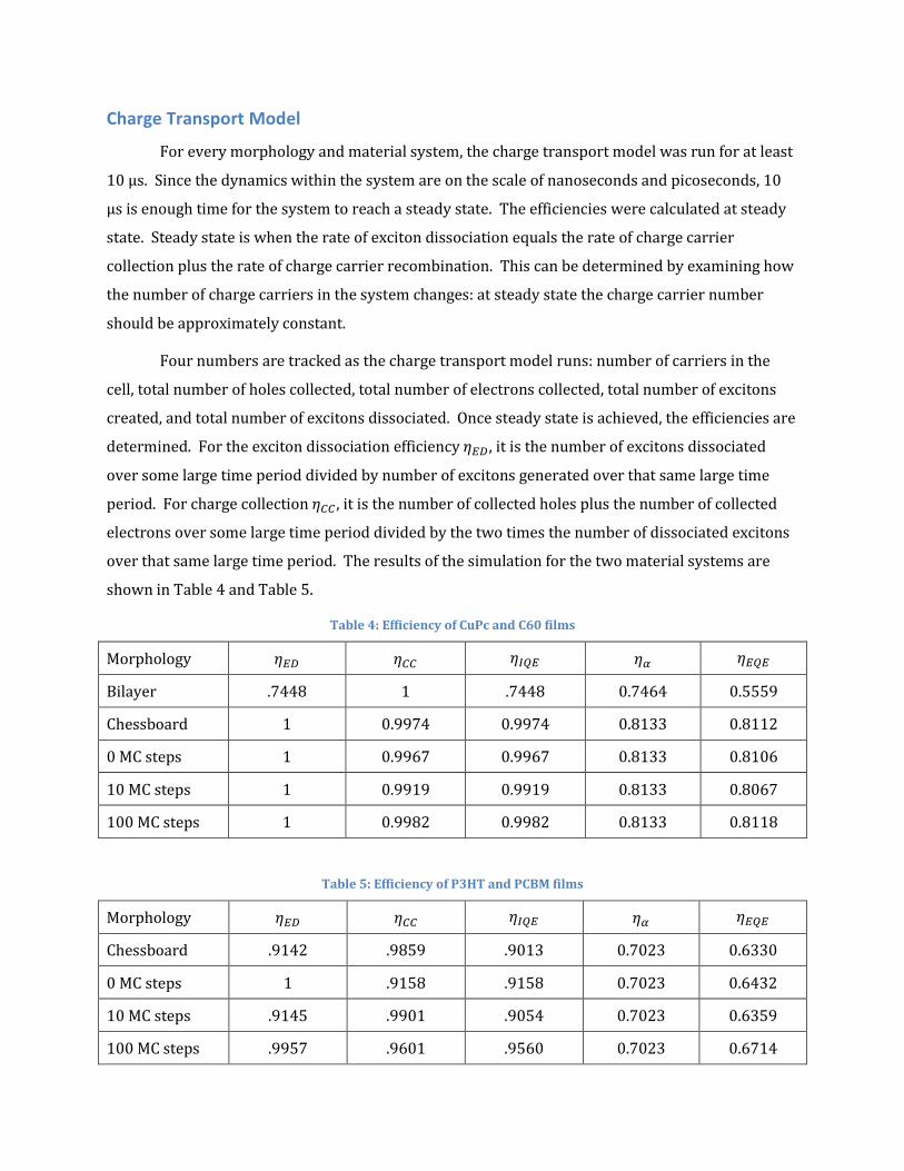
For every morphology and material system, the charge transport model was run for at least
10 μs. Since the dynamics within the system are on the scale of nanoseconds and picoseconds, 10
μs is enough time for the system to reach a steady state. The efficiencies were calculated at steady
state. Steady state is when the rate of exciton dissociation equals the rate of charge carrier
collection plus the rate of charge carrier recombination. This can be determined by examining how
the number of charge carriers in the system changes: at steady state the charge carrier number
should be approximately constant.
Four numbers are tracked as the charge transport model runs: number of carriers in the
cell, total number of holes collected, total number of electrons collected, total number of excitons
created, and total number of excitons dissociated. Once steady state is achieved, the efficiencies are
determined. For the exciton dissociation efficiency , it is the number of excitons dissociated
over some large time period divided by number of excitons generated over that same large time
period. For charge collection , it is the number of collected holes plus the number of collected
electrons over some large time period divided by the two times the number of dissociated excitons
over that same large time period. The results of the simulation for the two material systems are
shown in Table 4 and Table 5.
Table 4: Efficiency of CuPc and C60 films
Morphology
Bilayer .7448 1 .7448 0.7464 0.5559
Chessboard 1 0.9974 0.9974 0.8133 0.8112
0 MC steps 1 0.9967 0.9967 0.8133 0.8106
10 MC steps 1 0.9919 0.9919 0.8133 0.8067
100 MC steps 1 0.9982 0.9982 0.8133 0.8118
Table 5: Efficiency of P3HT and PCBM films
Morphology
Chessboard .9142 .9859 .9013 0.7023 0.6330
0 MC steps 1 .9158 .9158 0.7023 0.6432
10 MC steps .9145 .9901 .9054 0.7023 0.6359
100 MC steps .9957 .9601 .9560 0.7023 0.6714

The average number of charge carriers in the cell is directly related to the carrier collection
efficiency. The larger the average number of carriers is, the smaller the efficiency will be. For the
CuPc:C60 material system, the average number of charge carriers was 0.93 for the bilayer and up to
7.63 for the 0 MC step BHJ. This is compared to the lowest average of 25.32 for the chessboard of
P3HT:PCBM. Accordingly, the efficiencies for the CuPc:C60 morphologies are higher than their
P3HT:PCBM counter parts.
Largely, the values obtained make sense. The perfect exciton diffusion efficiencies make
sense for CuPc:C60 because the exciton diffusion length is 15 nm and 40 nm for CuPc and C60
respectively. The chessboard morphology’s columns are only 5 nm by 5 nm and the BHJ
morphologies all had feature sizes less than 5 nm. Perfect dissociation efficiency makes sense. The
bilayer’s high dissociation efficiency is also understandable because the CuPc and C60 layers are 20
nm and 40 nm thick respectively, very close to the diffusion length for those materials. The only
slightly troubling item is that the charge collection efficiency is higher for 0 MC step BHJ compared
to 10 MC step BHJ contrary to theory. However, the difference is so minute and their average
carrier number so close (7.63 compared to 6.23) that this result could be an artifact from the
efficiency calculation.
For the P3HT and PCBM morphology, everything is consistent with predicted trends except
for 100 MC steps. The values for 100 MC steps are out of step with every trend. Large feature sizes
should result in lower exciton dissociation and higher charge collection but the opposite is
observed for the 100 MC step morphology.
Discussion
The results from the CuPc:C60 tests generally do not match the corresponding results from
the work done by Yang and Forrest. They simulated a of 0.25 for the 60 nm bilayer compared
to the value of 0.7448 presented here. For BHJ morphologies with similar characteristic feature
sizes, they had = 0.34 compared to the near unity values obtained here. Several possible
reasons for these discrepancies are discussed here.
Yang and Forrest did not account for a PEDOT-PSS layer when computing the exciton
generation rate and distribution. They also did not state how thick their ITO layer was assumed to
be, and also they used a silver contact of unknown thickness compared to the aluminum contact
used here. Furthermore, the indices of refractions for these materials can vary a fair amount
depending on how they are deposited, and it is unknown exactly what numbers Yang and Forrest

used for their calculation. Also to be considered are the many edge cases in the charge transport
simulation that were not fully explained such as what happens when a hole tries to recombine with
an electron, but the electron is no longer there.
However, the largest difference from Yang and Forrest’s work is the exciton hopping time.
The version used in this work can be seen in Equation 29. The key is that the exciton localization
radius was fitted so that the excition should diffuse the correct amount given its lifetime. Yang
and Forrest used the following:
(
)
(32)
where is the diffusion length of the excition. An excition in CuPc will have a diffusion length of
15 nm. Assuming
= 1, and = 1 nm (which it generally is), then this exciton will have a
hop time of 9E-16 seconds or a hop time of 900 attoseconds. This corresponds to 1.1E7 hops for
one exciton lifetime. If the exciton moves like a particle undergoing a random walk, then it will
travel the square root of 1.1E7 nm for a distance of 3375 nm which is significantly larger than its
diffusion length of 15 nm. In fact, using this equation should give Yang and Forrest perfect excition
dissociation for every morphology. They did not report perfect dissociation so it seems there is a
mistake somewhere.
The performance for the P3HT:PCBM makes more sense. From the literature, internal
quantum efficiencies of 0.8 have been reported [20] [21]. The simulated IQE of 0.9 presented here
is not that different from these experimental values. Also, the parameters for P3HT:PCBM films can
vary greatly depending on how they are constructed or measured. For example 21 nm was the
exciton diffusion length used for P3HT in the simulation; however some researchers have reported
diffusion lengths as low as 3 nm [22] . This could greatly change the final simulation values.
Conclusions and Future Work
A Dynamical Monte Carlo simulation has been developed to simulate organic solar cell
performance. Besides just the charge transport simulation model, all accompanying tools needed to
simulate a variety of organic solar cells have also been constructed. These tools include code to
calculate exciton generation rate and distribution, generate random bulk heterojunction
morphologies, classify those bulk heterojunction morphologies according to characteristic feature
size, and generate figures of those BHJ morphologies. Even though everything was originally

designed to be used with the CuPc:C60 material system, it was a simple procedure to convert to the
P3HT:PCBM system and generate results close to experimental values.
Future work be will focused on further testing of the P3HT:PCBM material system such as
simulations of BHJ morphologies with bigger domain sizes, changing the input parameters, more
trials of current morphologies, etc. Eventually the goal will be experimental confirmation of the
simulation results and eventual usage of the simulation to help guide solar cell design.
Acknowledgements
I would like to thank Prof Adrienne D. Stiff-Roberts for her immense amount of patience as
she guided me on this work. I also thank Prof. Ian Dinwoodie for talking to me about Monte Carlo
simulations, Prof. Robert Brown for explaining some issues I had with computer based Monte Carlo
simulations, and Prof Stephen Teitsworth for helpful conversations. I would also like to thank Ryan
McCormick for always being there to listen and offer advice whenever I hit a roadblock. Lastly, I
would like to thank Dean Martha Absher for the opportunity offered by her Pratt Fellows Program.
Works Cited
[1] C. W. Tang, "Two-Layered Organic Photovoltaic Cell," Appl. Phys. Lett., vol. 48, pp. 183-185,
1986.
[2] M. A. Green, K. Emery, Y. Hishikawa, W. Warta and E. D. Dunlop, ""Solar cell efficiency tables
(version 39)"," Progress in Photovoltaics: Research and Applications,, vol. 20, pp. 12-20, 29
February 2012.
[3] L. Li, "Dissertation: Charge Transport in Organic Semiconductor Materials and Devices,"
Vienna University of Technology, Vienna, 2007.
[4] P. Peumans, A. Yakimov and S. R. Forrest, "Small Molecular Weight Organic Thin-Film
Photodetectors and Solar Cells," J. Appl. Phys., vol. 93, pp. 3693-3723, 2003.
[5] P. K. Watkins, A. B. Walker and G. L. Verschoor, "Dynamical Monte Carlo Modelling of Organic
Solar Cells: The Dependence of Internal Quantum Efficiency on Morphology," Nano Letters, vol.
5, no. 9, pp. 1814-1818, 2005.
[6] F. Yang and S. R. Forrest, "Photocurrent Generation in Nanostructured Organic Solar Cells," ACS

Nano, vol. 2, no. 5, pp. 1022-1032, 2008.
[7] P. Peumans, Y. Aharon and F. R. Stephen, "Erratum: "Small molecular weight organic thin-film
photodetectors and solar cells" [J. Appl. Phys. 93, 3693 (2003)]," J. Appl. Phys., vol. 95, no. 5, p.
2938, 2004.
[8] D. Datta, V. Tripathi, P. Gogoi, S. Banerjee and S. Kumar, "Ellipsometric studies on thin film
CuPC:C60 blends for solar cell applications," Thin Solid Films, vol. 516, pp. 7237-7240, 2008.
[9] F. Monestier, J. Simon, P. Torchio, L. Escoubas, F. Flory, S. Bailly, R. de Bettignies, S. Guillerez
and C. Defranoux, "Modeling the short-circuit current density of polymer solar cells based on
P3HT:PCBM blend," Sol. Energy Mater. Sol Cells, 2006.
[10] H. Hoppe, N. S. Sariciftci and D. Meissner, "Optical Constants of Conjugate Polymer/Fullerene
Based Bulk-Heterojunction Organic Solar Cells," Mol. Cryst. Liq. Cryst., vol. 385, pp. 233-239,
2002.
[11] M. Polyanskiy, "Refractive Index Database," 2012. [Online]. Available:
http://refractiveindex.info/. [Accessed 19 March 2012].
[12] H. Bassler, "Charge transport in disordered organic photoconductors," Phys. Stat. Sol.(b), vol.
175, pp. 15-55, 1993.
[13] A. Miller and E. Abrahams, "Impurity Conduction at Low Concentrations," Physical Review, vol.
120, no. 3, pp. 745-755, 1960.
[14] J. Szmytkowski, "Modeling the electrical characteristics of P3HT:PCBM bulk heterojunction
solar cells: Implementing the interface recombination," Semicond. Sci. Technol, vol. 25, 2010.
[15] P. P. Boix, G. Garcia-Belmonte, U. Munecas, M. Neophytou, C. Waldauf and R. Pacios,
"Determination of gap defect states in organic bulk heterojunction solar cells from capacitance
measurements," Appl. Phys. Lett, vol. 95, 2009.
[16] V. S. Gevaerts, L. Jan Anton Koster, M. M. Wienk and R. A. Jansen, "Discriminating between
Bilayer and Bulk Heterojunction Polymer:Fullerene Solar Cells Using the External Quantum
Efficiency," ACS Appl. Mater. Interfaces, vol. 3, pp. 3252-3255, 2011.
[17] K. S. Nalwa, H. K. Kodali, B. Ganapathysubramanian and S. Chaudhary, "Dependence of
recombination mechanisms and strength on processing conditions in polymer solar cells,"

Appl. Phys. Lett., vol. 99, 2011.
[18] T. Erb, U. Zhokhavets, G. Gobsch, S. Raleva, B. Stuhn, P. Schilinsky, C. Waldauf and C. J. Brabec,
"Correlation Between Structural and Optical Properties of Composite Polymer/Fullerne Films
for Organic Solar Cells," Adv. Funct. Mater., vol. 15, pp. 1193-1196, 2005.
[19] R. A. Marsh, C. Groves and N. C. Greenham, "A microscopic model for the behavior of
nanostructured organic photovoltaic devices," J. Appl. Phys., vol. 101, 2007.
[20] J. Jo, S. Na, S. Kim, T. Lee, Y. Chung, S. Kang, D. Vak and D. Kim, "Three-Dimensional Bulk
Heterojunction Morphology for Achieving High Internal Quantum Efficiency in Polymer Solar
Cells," Adv. Func. Mater., vol. 19, pp. 2398-2406, 2009.
[21] G. F. Burkhard, E. T. Hoke and M. D. McGehee, "Accounting for Interference, Scattering, and
Electrode Absorption to Make Accurate Internal Quantum Efficiency Measurements in Organic
and Other Thin Solar Cells," Adv. Mater., vol. 22, pp. 3293-3297, 2010.
[22] P. E. Shaw, A. Ruseckas and I. D. Samuel, "Excition Diffusion Measurments in Poly(3-
hexylthiophene)," Adv. Mater., vol. 20, no. 18, pp. 3516-3520, 2008.
[23] M. Pope, Electronic Processes in Organic Crystals and Polymers, Oxford University Press, 1999.
[24] S. E. Shaheen, N. Kopidakis, D. S. Ginley, M. S. White and D. C. Olson, "Inverted bulk-
heterojunction plastic solar cells," SPIE Newsroom, 24 May 2007. [Online]. Available:
http://spie.org/x14269.xml. [Accessed 14 April 2012].
[25] V. Sundström and C. S. J. Ponseca, "Transport in organic solar-cell materials studied by time-
resolved terahertz spectroscopy," Lund University, 29 October 2007. [Online]. Available:
http://www.chemphys.lu.se/research/projects/teratransport/. [Accessed 14 April 2012].