prospect for the memory packaging technology - ectc.net · sk hynix is leading new and advanced...
TRANSCRIPT
Prospect for the memory Packaging technology
Nam-Seog Kim, Ph.D.Vice President,
P&T Technology Group
SK hynix Inc.

Agenda
1. Electronic Packaging Trend
2. Memory Packaging Roadmap
3. Innovative Packaging Technology- Package
- Process
- Material
4. Conclusion
3 / 14
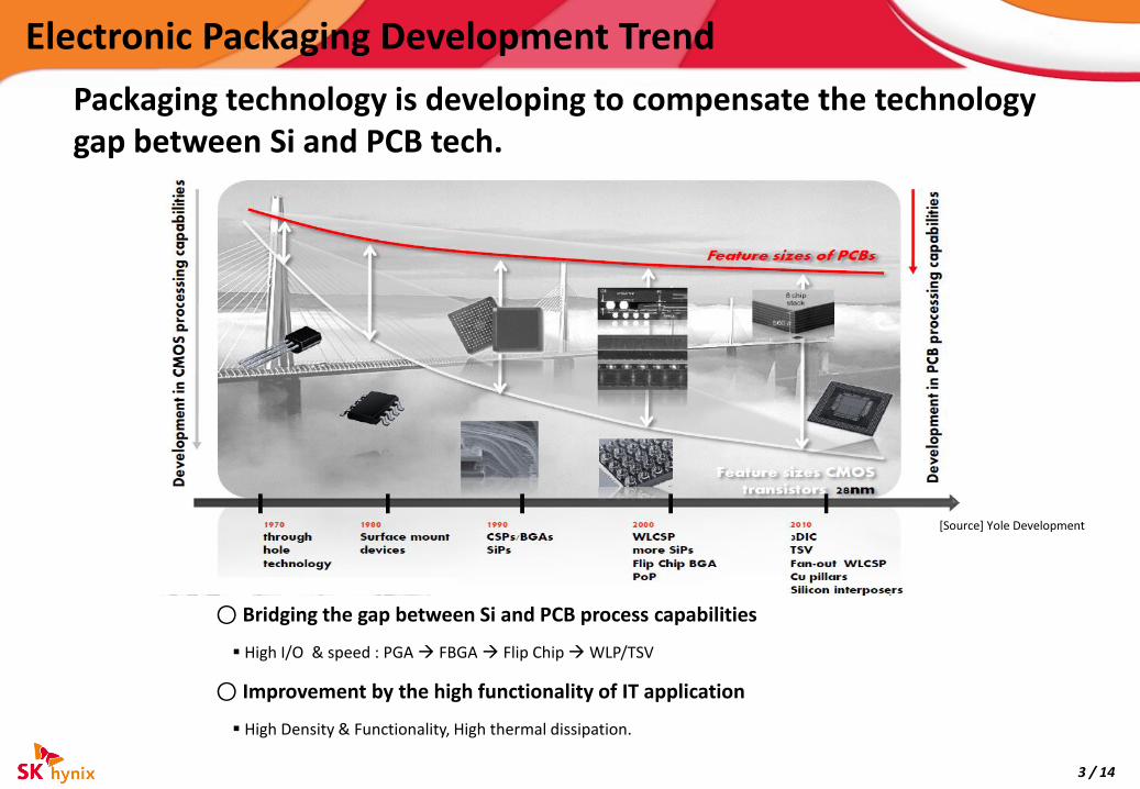
Packaging technology is developing to compensate the technology gap between Si and PCB tech.
Electronic Packaging Development Trend
[Source] Yole Development
○ Bridging the gap between Si and PCB process capabilities
High I/O & speed : PGA FBGA Flip Chip WLP/TSV
○ Improvement by the high functionality of IT application
High Density & Functionality, High thermal dissipation.
4 / 14
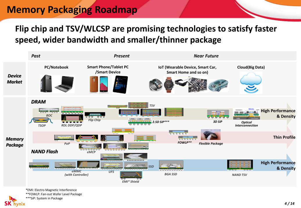
Smart Phone/Tablet PC/Smart Device
IoT (Wearable Device, Smart Car, Smart Home and so on)
PC/Notebook
Flip Chip
FOWLP**
EMI* Shield
3D SiP
Flexible Package
Optical Interconnection
Device Market
Memory Package
DRAM
NAND Flash
Cloud(Big Data)
High Performance & Density
Thin Profile
High Performance & Density
TSV
Past Present Near Future
eMCP
BOC
RDL DDP/QDP
Flip chip and TSV/WLCSP are promising technologies to satisfy faster speed, wider bandwidth and smaller/thinner package
Memory Packaging Roadmap
*EMI: Electro Magnetic Interference**FOWLP: Fan-out Wafer Level Package***SiP: System in Package
2.5D SiP***
eMMC(with Controller)
TSOP
PoP
BGA SSD NAND TSV
SSD
UFS

5 / 14
AP & Memory package stack is widely being used.
① Package Stack
Mobile Application: AP + Memory Top/Bottom PKG Warpage Control
PoP (Package on Package)
Innovative Packaging Technology - Package
6 / 14
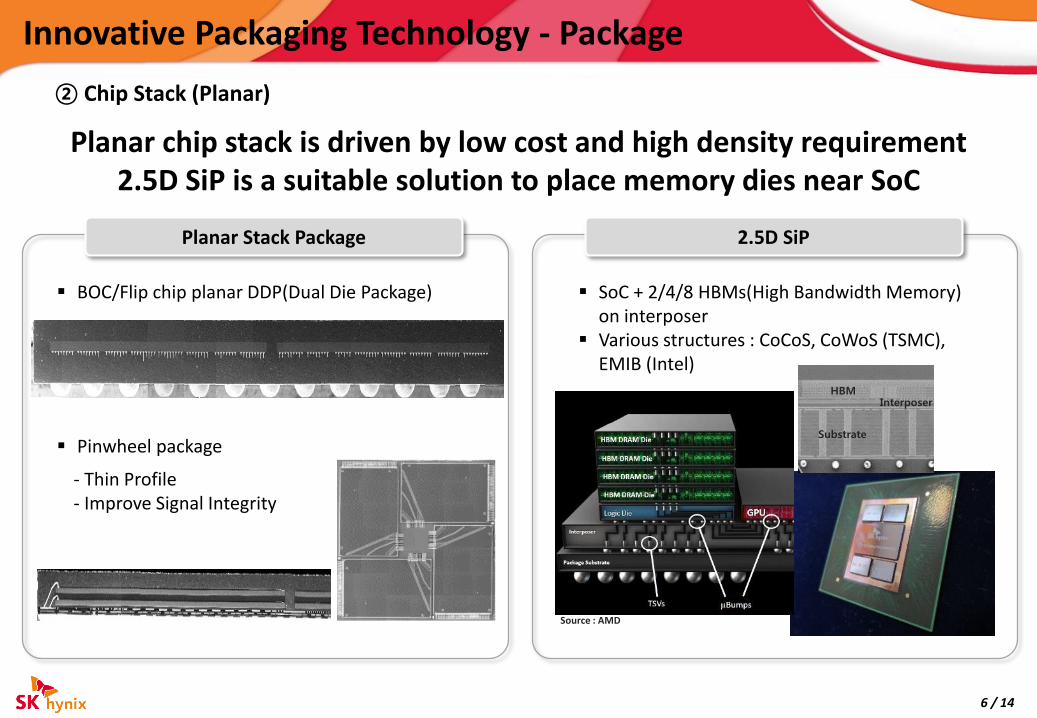
② Chip Stack (Planar)
HBM
SoC + 2/4/8 HBMs(High Bandwidth Memory) on interposer
Various structures : CoCoS, CoWoS (TSMC), EMIB (Intel)
Planar chip stack is driven by low cost and high density requirement2.5D SiP is a suitable solution to place memory dies near SoC
BOC/Flip chip planar DDP(Dual Die Package)
Pinwheel package
Source : AMD
HBMInterposer
Substrate
Planar Stack Package 2.5D SiP
Innovative Packaging Technology - Package
- Thin Profile- Improve Signal Integrity
7 / 14
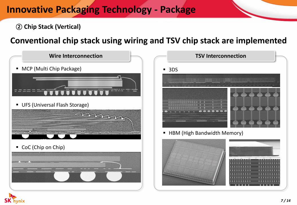
Conventional chip stack using wiring and TSV chip stack are implemented
② Chip Stack (Vertical)
MCP (Multi Chip Package) 3DS
Wire Interconnection TSV Interconnection
UFS (Universal Flash Storage)
CoC (Chip on Chip)
HBM (High Bandwidth Memory)
Innovative Packaging Technology - Package
8 / 14
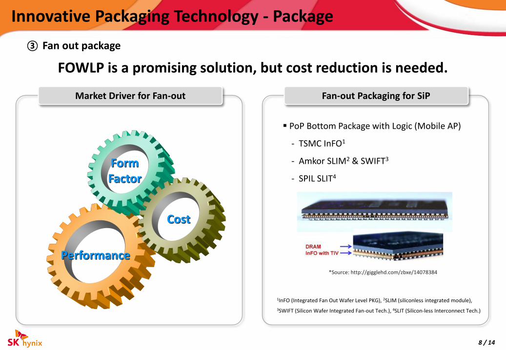
③ Fan out package
*Source: http://gigglehd.com/zbxe/14078384
FOWLP is a promising solution, but cost reduction is needed.
PoP Bottom Package with Logic (Mobile AP)
- TSMC InFO1
- Amkor SLIM2 & SWIFT3
- SPIL SLIT4
1InFO (Integrated Fan Out Wafer Level PKG), 2SLIM (siliconless integrated module),
3SWIFT (Silicon Wafer Integrated Fan-out Tech.), 4SLIT (Silicon-less Interconnect Tech.)
Innovative Packaging Technology - Package
Performance
Cost
FormFactor
Market Driver for Fan-out Fan-out Packaging for SiP
9 / 14
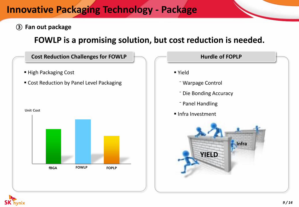
③ Fan out package
Yield
⁻ Warpage Control
⁻ Die Bonding Accuracy
⁻ Panel Handling
Infra Investment
FOWLP is a promising solution, but cost reduction is needed.
High Packaging Cost
Cost Reduction by Panel Level Packaging
Innovative Packaging Technology - Package
fBGA FOWLP FOPLP
Unit Cost
YIELD
Infra
Hurdle of FOPLPCost Reduction Challenges for FOWLP
10 / 14
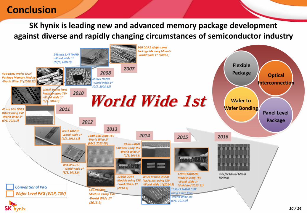
20072008
2010
2012
20132014 2015 2016
2011
Conventional PKG
Wafer Level PKG (WLP, TSV)
128GB LRDIMM Module using TSV -World Wide 1st
(Validated 2015.11)
24Stack 1.4T NAND -World Wide 1st
(M/S, 2007.9)
2Stack Wafer level Package using TSV -World Wide 1st
(E/S, 2010.3)
29 nm HBM1 5mKGSD using TSV
-World Wide 1st
(C/S, 2014.9)
SK hynix is leading new and advanced memory package development against diverse and rapidly changing circumstances of semiconductor industry
2GB DDR2 Wafer Level Package Memory Module-World Wide 1st (2007.1)
4GB DDR2 Wafer Level Package Memory Module-World Wide 1st (2008.12)
8Stack NAND-World Wide 1st
(C/S, 2008.12)
Flexible
Package Optical
Interconnection
Panel Level
Package
Wafer to
Wafer Bonding
Conclusion
40 nm 2Gb DDR3 8stack using TSV -World Wide 1st
(E/S, 2011.3)
WIO1 4KGSD-World Wide 1st
(E/S, 2012.11)
WLCSP 0.37T- World Wide 1st
(E/S, 2013.9)
128GB DDR4 Module using TSV -World Wide 1st
(2014.3)
WIO2 Mobile DRAM(4x Faster) using TSV-World Wide 1st(2014.9)
3DS for 64GB/128GB RDIMM
64GB DDR4 Module using TSV -World Wide 1st
(2013.9)
World Wide 1st
16mKGSD using TSV -World Wide 1st
(M/S, 2013.09 )
16Stack NAND 0.9T using 15um Chip-World Wide 1st(E/S, 2014.9)

Thanks for Your Time