series editors markku lahti technica a scientiae rerum
TRANSCRIPT

ABCDEFG
UNIVERS ITY OF OULU P.O.B . 7500 F I -90014 UNIVERS ITY OF OULU F INLAND
A C T A U N I V E R S I T A T I S O U L U E N S I S
S E R I E S E D I T O R S
SCIENTIAE RERUM NATURALIUM
HUMANIORA
TECHNICA
MEDICA
SCIENTIAE RERUM SOCIALIUM
SCRIPTA ACADEMICA
OECONOMICA
EDITOR IN CHIEF
PUBLICATIONS EDITOR
Professor Mikko Siponen
University Lecturer Elise Kärkkäinen
Professor Hannu Heusala
Professor Olli Vuolteenaho
Senior Researcher Eila Estola
Information officer Tiina Pistokoski
University Lecturer Seppo Eriksson
Professor Olli Vuolteenaho
Publications Editor Kirsti Nurkkala
ISBN 978-951-42-8893-7 (Paperback)ISBN 978-951-42-8894-4 (PDF)ISSN 0355-3213 (Print)ISSN 1796-2226 (Online)
U N I V E R S I TAT I S O U L U E N S I SACTAC
TECHNICA
U N I V E R S I TAT I S O U L U E N S I SACTAC
TECHNICA
OULU 2008
C 303
Markku Lahti
GRAVURE OFFSET PRINTING FOR FABRICATION OF ELECTRONIC DEVICES AND INTEGRATED COMPONENTS IN LTCC MODULES
FACULTY OF TECHNOLOGY,DEPARTMENT OF ELECTRICAL AND INFORMATION ENGINEERING,INFOTECH OULU,UNIVERSITY OF OULU;THE GRADUATE SCHOOL FOR ELECTRONICS, TELECOMMUNICATIONS AND AUTOMATION, GETA,HELSINKI UNIVERSITY OF TECHNOLOGY
C 303
ACTA
Markku Lahti
C303etukansi.fm Page 1 Wednesday, September 10, 2008 9:35 AM


A C T A U N I V E R S I T A T I S O U L U E N S I SC Te c h n i c a 3 0 3
MARKKU LAHTI
GRAVURE OFFSET PRINTING FOR FABRICATION OF ELECTRONIC DEVICES AND INTEGRATED COMPONENTS IN LTCC MODULES
Academic dissertation to be presented, with the assent ofthe Faculty of Technology of the University of Oulu, forpublic defence in Raahensali (Auditorium L10), Linnanmaa,on October 10th, 2008, at 12 noon
OULUN YLIOPISTO, OULU 2008

Copyright © 2008Acta Univ. Oul. C 303, 2008
Supervised byProfessor Vilho Lantto
Reviewed byAssociate Professor Andrzej DziedzicDoctor Anthony J. Moulson
ISBN 978-951-42-8893-7 (Paperback)ISBN 978-951-42-8894-4 (PDF)http://herkules.oulu.fi/isbn9789514288944/ISSN 0355-3213 (Printed)ISSN 1796-2226 (Online)http://herkules.oulu.fi/issn03553213/
Cover designRaimo Ahonen
OULU UNIVERSITY PRESSOULU 2008

Lahti, Markku, Gravure offset printing for fabrication of electronic devices andintegrated components in LTCC modulesFaculty of Technology, Department of Electrical and Information Engineering, Infotech Oulu,University of Oulu, P.O.Box 4500, FI-90014 University of Oulu, Finland; The Graduate Schoolfor Electronics, Telecommunications and Automation, GETA, Helsinki University ofTechnology, P.O. Box 3000, FI-02015 TKK, Finland Acta Univ. Oul. C 303, 2008Oulu, Finland
AbstractThe thesis is concerned with the development of gravure-offset-printing and low temperature co-fired ceramic (LTCC) technologies for the miniaturisation of electronic devices and components.The development work has been verified by several applications.
Several aspects of gravure-offset-printing have to be optimised in order to make it suitable forfine-line printing and these have been addressed in the study with a focus on the printing inks andplates. Gravure-offset-printing inks were developed from commercial thick-film pastes. Theeffects of different ink characteristics on some properties of conductor lines, such as line widthand resistivity, were studied. The dependence of the conductor lines on the quality of theengravings in the printing plates was also studied. The narrowest line widths obtained were about30 μm with an accuracy of ±5 μm.
Various LTCC compositions and processing steps involved in the production of integratedelectronic devices, and the properties of several fabricated devices are discussed. The devicesinclude inductors, band-pass filters and resistors for the 1–2 GHz frequency range. Miniaturisationhas been the main focus of attention. For example, the integration of high-permittivity tapes inaddition to low-permittivity tapes has made the miniaturisation of filter structures possible.Compatibility between these tapes during firing was found to be good.
LTCC technology was further developed by adapting a modified LTCC-on-metal (LTCC-M)approach. A traditional way of guiding heat away from a component is to place a heat-sink underthe component and utilise thermal vias and solder balls. In this study high- and low-permittivitytapes were attached directly on a heat-sink. Different heat-sink options were evaluated and the bestperformance was achieved with an AlN heat-sink which was deposited by screen-printing a Aulayer on it. High-power chips were attached directly on the heat-sink through cavities in the LTCCtapes. This approach also restricted the shrinkage of the LTCC tapes. The fabricated test structuresand components proved the viability of the approach although the compatibility between thepastes and tapes was not optimal.
Keywords: gravure-offset-printing, heat management, LTCC, LTCC-M, passivecomponents


5
Acknowledgements
The work reported in this thesis was carried out at the Microelectronics and Materials Physics Laboratories, University of Oulu between the years 1993 and 2000, and at VTT between the years 2001 and 2007. Between the years 1996 and 1999 the author was a member of the Graduate School for Electronics, Telecommunication and Automation (GETA) in Finland.
I wish to express my best gratitude to my supervisor Professor Vilho Lantto for his expert guidance and support. I also thank Professor Seppo Leppävuori for a possibility to make this work.
I would like to thank Professor Andrzej Dziedzic and late Dr. A.J. Moulson for reviewing the thesis and for their constructive comments on the thesis. Late Dr. A.J. Moulson is also acknowledged for revising the English of the manuscript.
Especially I want to thank my colleagues Mrs. Katri Kukkola, Mr. Juha Väänänen and Dr. Janne Remes for their help and guidance with gravure-offset-printing and Mr. Kari Kautio for his help with LTCC processing. The staffs of the Microelectronics and Materials Physics Laboratories at the University of Oulu and of the Micromodules Centre at VTT are acknowledged for pleasant working atmospheres.
This work has been financially supported by the Academy of Finland, Tauno Tönningin Säätiö, Suomen Kulttuurirahasto, Oulun yliopiston tukisäätiö, Ulla Tuomisen säätiö, Tekniikan edistämissäätiö and Seppo Säynäjäkankaan Tiedesäätiö, all of which are gratefully acknowledged.
Finally, I want to express my gratitude to my family, Yujie and Jenni, for their patience during the course of this thesis.

6

7
List of original papers
The thesis is based on the following seven papers, which will be referred to in the text by their Roman numerals.
I Lahti M, Kukkola K & Leppävuori S (1995) The utilising of gravure offset printing for miniaturising of electronic packages. Microelectronics International 37: 22–24.
II Lahti M, Leppävuori S & Lantto V (1999) Gravure-offset-printing technique for the fabrication of solid films. Applied Surface Science 142: 367–370.
III Lahti M, Lantto V & Leppävuori S (2000) Planar inductors on an LTCC substrate realised by the gravure-offset-printing technique. IEEE Transactions on Components and Packaging Technology 23(4): 606–610.
IV Lahti M & Lantto V (2001) Passive RF band-pass filters in an LTCC module made by fine-line thick-film pastes. Journal of the European Ceramic Society 21: 1997–2000.
V Lahti M, Vimpari A & Kautio K (2007) Printable resistors in LTCC systems. Journal of the European Ceramic Society 27(8–9): 2953–2956.
VI Lahti M, Kautio K, Juntunen E, Petäjä J & Karioja P (2006) Improving thermal management of LTCC modules by laminating and co-firing tapes directly on a heat sink. Proc European Microelectronics and Packaging Symposium, May 22–24, Terme Catez, Slovenia: 155–158.
VII Lahti M, Kautio K & Karioja P (2006) Integrated LTCC modules by laminating and co-firing tapes directly on heat sink. Proc. 36th European Microwave Conference, September 11–15, 2006, Manchester, United Kingdom:476–479.
The three aspects of the research have been reported in the scientific literature. Papers I and II report the results obtained from studies concentrating on the development of the gravure-offset-printing process. Papers III, IV and V present results from applications realised by the gravure-offset-printing and screen-printing techniques on LTCC substrates. Papers VI and VII focus on the development of heat-management in LTCC technology.
The experimental work in Paper I was carried out by the author and Mrs. Kukkola. In Papers V, VI and VII the design and fabrication was undertaken in close co-operation between the authors. In other papers the designs, realisations and measurements of the samples were made solely by the author. The manuscripts were written by the author with the help of the co-authors.

8

9
List of symbols and abbreviations
εr relative permittivity Q quality factor Ra surface roughness APLAC Computer program: “Analysis Program for Linear Active Circuits” CTE coefficient of thermal expansion DCA dynamic contact angle ESL Electro Science Laboratories FR-4 Flame Retardant 4 HTCC high temperature co-fired ceramic IC integrated circuit LTCC low temperature co-fired ceramic LTCC-M low temperature co-fired ceramic on metal MCM-D deposited multi-chip modules MCM-L laminated multi-chip modules MMIC monolithic microwave integrated circuit Nd-YAG neodymium-doped yttrium aluminum garnet PCB printed circuit board RF radio frequency SEM scanning electron microscopy UHF ultra high frequency UV ultra violet

10

11
Contents Abstract Acknowledgements 5 List of original papers 7 List of symbols and abbreviations 9 Contents 11 1 Introduction 13
1.1 Fine-line thick-film printing technologies............................................... 13 1.2 Thick-film multi-layer processing........................................................... 14 1.3 Motivation for the research and thesis outline ........................................ 16
2 Gravure-offset-printing 17 2.1 Description of the process....................................................................... 17 2.2 Key elements of the gravure-offset-printing process .............................. 19
2.2.1 Printing plates............................................................................... 19 2.2.2 Conductor inks ............................................................................. 20 2.2.3 Silicone rubber pads and rollers ................................................... 20 2.2.4 Printing parameters....................................................................... 21 2.2.5 Substrates ..................................................................................... 21 2.2.6 Printing machines ......................................................................... 21
3 Low Temperature Co-Fired Ceramics (LTCCs) 23 3.1 Processing of LTCCs............................................................................... 23 3.2 Typical LTCC compositions.................................................................... 25 3.3 Heat-management methods in LTCC technology ................................... 28 3.4 Some concerns in the processing of LTCC structures............................. 29
3.4.1 Metallisation................................................................................. 29 3.4.2 Control of shrinkage ..................................................................... 30
3.5 Typical properties of LTCC materials ..................................................... 32 3.6 Some integrated circuit applications exploiting LTCC structures........... 33
3.6.1 Overview of passive components ................................................. 33 3.6.2 Passive components integrated with LTCC modules ................... 36 3.6.3 Other integrated electronics applications exploiting LTCC
structures ...................................................................................... 38 4 Experimental work 39
4.1 Gravure-offset-printing ........................................................................... 40 4.2 Production of passive components.......................................................... 42
4.2.1 Simulation and design .................................................................. 42

12
4.2.2 Processing steps............................................................................ 44 4.3 Heat-management development utilising zero-shrinkage LTCC
systems .................................................................................................... 47 4.4 Measurements ......................................................................................... 48
4.4.1 Printing inks.................................................................................. 48 4.4.2 Test measurements for printed patterns ........................................ 49 4.4.3 Electrical measurements ............................................................... 49
5 Results and discussion 51 5.1 The basics of gravure-offset-printing ...................................................... 51
5.1.1 Printing inks.................................................................................. 51 5.1.2 The effects of the printing plate on printing quality ..................... 52 5.1.3 Other factors ................................................................................. 53
5.2 Gravure-offset-printing inks for LTCC tapes .......................................... 54 5.3 Study of planar inductors ........................................................................ 56
5.3.1 Computer simulations................................................................... 56 5.3.2 Planar inductors integrated into a LTCC module ......................... 56
5.4 Study of filters......................................................................................... 58 5.4.1 Computer simulations................................................................... 58 5.4.2 Fabrication.................................................................................... 58 5.4.3 Electrical performance of filters ................................................... 58 5.4.4 Comparison between simulated and measured values.................. 59
5.5 Study of resistors..................................................................................... 60 5.6 Heat-management in the case of LTCC-M approach .............................. 61
6 Summary and suggestions for future work 63 References 67 Original papers 73

13
1 Introduction
1.1 Fine-line thick-film printing technologies
The use of the screen-printing technique in electronics was started by IBM in the 1960’s [1] and although it is a well-known and an economic manufacturing method in mass production, some problems exist. One of the driving forces in the manufacturing of electronic circuits is miniaturisation. The realisation of narrow (<100 µm wide) conductor lines by screen-printing is difficult and therefore other thick-film deposition methods have been developed [2]. With screen-printing it is also difficult to produce conductors with the smooth surface and precise edges that are needed, for example in high-frequency applications [3].
The screen-printing approach itself has been developed by introducing improved pastes and screens, and by optimising printing parameters. The improved screens include, for example, etched solid metal masks and electroformed masks. Also screens with higher mesh count (number of apertures per linear unit length) have been developed and nowadays there are screens available which have as high a mesh count as 640. The meshed wires can be replaced by stencils where the pattern has been etched in a pseudo-meshed way. By these more advanced methods 50 µm wide conductors have been printed [4,5]. Development of photoimageable thick-film pastes has allowed a further miniaturisation of conductor lines. These pastes include vehicles which are processed by exposing and developing them with appropriate solvent before firing. The realisation of conductor lines with line-widths down to 15 µm has been reported [6]. A disadvantage of the process is the high capital costs of the equipment needed to expose and develop these photosensitive pastes. Another possibility is to etch special thick-film pastes after resist film patterning. This allows an improvement of the circuit performance, which is comparable to that of thin-film circuits, especially at high frequencies [7].
In addition to the improvements in the screen-printing other thick-film approaches have also been developed. In thick-film direct writing, conductors and dielectrics are deposited through a nozzle onto a substrate. In this way most of the normal thick-film production steps can be avoided and a more uniform circuit performance can be achieved [8]. Also laser irradiation has been utilised in the realisation of narrow conductor lines. In this technique the paste is spin-coated onto a substrate followed by the laser beam irradiation. Eventually the non-

14
irradiated pastes are removed by using organic solvent. This technique has allowed the realisation of 20 µm wide lines [9]. Gravure-offset-printing is also one of these fine-line thick-film techniques. In this technique patterns to be printed are realised in printing plates instead of screens and as narrow as 25 µm wide conductor lines have been printed. Typical fired thickness and square resistance values have been 1.0–1.2 µm and 30–40 mΩ/ [10].
Gravure-offset-printing, which is also known as pad-printing or tampo-printing, is also an old printing technique that has been used in decorative applications for a long time [11]. The first references for the use of the technique in electronics manufacturing are from the beginning of 1990’s [12]. This technique makes it possible to print narrow conductor lines on substrates of various materials and shapes due to the flexibility of the silicone rubber pad. Ink wastage is less than in the case of screen-printing and the recycling of inks is also easier [13]. A disadvantage in comparison with screen-printing is a lower conductor thickness which is typically in the range of a few µm after a single print. Gravure-offset-printing has been used for the production of, for example, solar cells and liquid crystal displays [2,14].
1.2 Thick-film multi-layer processing
The increased complexity of hybrid circuit designs requires the use of multi-layer structures. The methods in the 1970’s to realise multi-layer structures were mainly based upon either thick-film processing or high temperature co-fired ceramic (HTCC) materials.
In the thick-film technology the layers are built by consecutive printing and firing of conductive and insulating layers onto a substrate. Typically, the processing of each layer requires a conductor printing, two printings to fill via holes and at least two dielectric printings. These kinds of structures can require several firing steps. This limits the technology to structures where the number of conductor layers is low [15].
The HTCC multi-layer process uses tapes fabricated from slurry which contains a mixture of ceramic powder with 92–94% alumina content and an organic binder. In the technique based on the HTCC materials conductors are screen printed on an unfired ceramic tape. Typical conductor materials are refractory metals – molybdenum or tungsten. After the printing step, separate layers are laminated together to form a compact structure which is then co-fired at a temperature of 1600–1800 °C [16,17].

15
The HTCC process offers several advantages when compared to the thick-film multi-layer process. In thick-film multi-layer structures a thermal expansion mismatch between the dielectric and base substrate can cause warpage. The problems related to multiple firings can be avoided by using HTCC materials that need only a single firing step. There is also an improved isolation between the conductors due to the thick dielectric tape. In addition, printing of several dielectric layers can be eliminated. The HTCC approach also uses ceramics with high thermal conductivity, such as AlN and BeO in addition to Al2O3.
Naturally, there are some disadvantages associated with the HTCC process. The refractory conductors have higher resistivity in comparison with the noble metals used in thick-film hybrids. The co-fired process is not cost-effective in a prototype and small-scale production due to high costs of tooling. Passive components are not easy to integrate so they have to be assembled as discrete chips. In the case of the HTCC process a reducing atmosphere in firing is necessary to prevent oxidation of refractory metals, which also increases the costs. In addition, the lack of manufacturers of alumina tapes and the low electrical conductivity of the metals have restricted wide utilisation of HTCC technology. Refractory conductors also require plating to improve their corrosion resistance [18]. All these problems stimulated a need to combine the advantages of both thick-film and HTCC technologies. As a result, low temperature co-fired ceramic (LTCC) materials were introduced in the beginning of the 1980’s.
In low temperature co-fired ceramic materials the Al2O3 powder was replaced by a composition that could be sintered at a temperature below 1000 °C. It was possible to utilise the dielectric materials used in thick-film circuits in the development of LTCC materials. The advantages were, for example, a lower processing temperature, which made ceramic multi-layer processing compatible with the thick-film processing. Refractory metals could now be replaced by the high conductivity noble metals commonly used in thick-film processing, and the need for reducing atmosphere eliminated. Firing time was also reduced which increased throughput.
During the development process of LTCC materials the lower thermal conductivity of the glass-ceramic dielectric was the most serious disadvantage in comparison to alumina and restricted their use in high-power applications. In addition, the strength of the glass-ceramic composition was only about half that of alumina. Originally, silver was not an interesting alternative in the LTCC processing since the first applications were military-related and a good reliability was required. When the need arose to commercialise the materials highly

16
conductive and low cost metals such as silver were introduced. From the basic metal cost copper is attractive but the overall costs of using it are high because of the necessary reducing atmosphere in the co-firing process and the limited shelf life of copper powder [19]. The commercial use of LTCC materials was first seen in automotive applications in the 1990’s.
1.3 Motivation for the research and thesis outline
The aims of the study were to develop methods to increase the packaging density of electronic circuits by using thick-film technology and to demonstrate effectiveness by applications. There are several fields where high integration density can be utilised, for example, telecommunication and sensor applications. Gravure-offset-printing was considered suited to fine-line printing and, therefore, was chosen for a more detailed study. Another way to increase the packaging density is by exploiting multilayer structuring. As mentioned earlier, many reasons favour the use of the LTCC materials so they were chosen as substrate materials. Through a combination of gravure-offset-printing and LTCC technologies the miniaturisation of passive components and filters for applications in the UHF range was studied. The miniaturisation of components also set requirements for heat-management. This matter has also been addressed in the study.
The topics covered in the thesis are as follows. Chapter 2 introduces the basics of gravure-offset-printing. The processing and materials of LTCC technology are introduced in Chapter 3. The experimental work and results are summarised in Chapters 4 and 5. The studies are discussed in seven papers published in the scientific literature. Papers I and II give results on the development work of gravure-offset-printing. More details of the fabrication of inductors, filters and resistors are given in Papers III, IV and V, respectively. The experiments related to the heat-management methods are presented in Papers VI and VII.

17
2 Gravure-offset-printing
2.1 Description of the process
There are several lithographic processes where different types of printing plates or cylinders are involved and, in the case of gravure-offset-printing, they are described as "deep-etched" plates or cylinders meaning that the image areas are etched slightly below the level of their non-image areas [20]. The principle of gravure-offset-printing is illustrated in Fig. 1. The pattern to be printed is engraved on the plate by etching, for example, and the printing process involves first filling the engraving with ink by doctor-blading. In the present context the ink is a thick-film paste with suitably adjusted rheological properties. The pad is rolled over the filled plate picking up the ink pattern which is then transferred to the substrate by a similar rolling action. The rolling action is necessary to ensure that air is not trapped between pad and substrate. During transfer of the inked pad to the substrate evaporation of the ‘thinner’ occurs so that the paste has the optimum properties for its transference and adherence to the substrate. After printing the printed pattern is dried in order to evaporate the solvents. The final structure is obtained by firing with heat or UV light depending on the ink.
Fig. 1. The principle of the gravure-offset-printing process.
The process is sensitive to changes in the environment. This can be understood when one takes into account the low depth of the engravings which is about 25 µm. About half of the ink in the engravings is picked up and about 60% of this is a solvent which evaporates. Therefore the thickness of the dry ink deposit is only

18
about 5 µm. This kind of thin ink layer is susceptible to temperature variations, humidity level, static charges and airflow. Large amounts of static electricity are developed on the silicone rubber pads during printing. One way to decrease the amount of static electricity is to slow down the speed of the pad in making and releasing contact with a substrate. Slowing down the process allows also the reduction of small voids in the printed patterns [21].
There are several factors to be taken into account in the printing process. Fig. 2 shows in more detail the filling of the engravings. The ink reservoir lies on the plate and the blade is moving along the plate at an angle of α. Inevitably, because of a combination of the rheological properties of the paste and the surface properties of the blade, plate and paste, a small quantity of the ink penetrates under the blade leaving some ink on the non-image areas. By using a thinner doctor blade a more uniform and denser print can be obtained. The steeper doctor blade angle is preferred since wear of the cylinder and the blade becomes more uniform resulting in smaller density variations in the printed patterns [22].
Fig. 2. The influence of blade angle on the filling of the engravings [21].
Even if there is an excess of ink on the engraved plate it has been shown that only about 50% of the engraved volume is filled with ink following the doctor-blading process. The ink has a tendency to accumulate at the forward edge of the engraving and, although the ink tends to level out, the process may not be complete. There are several reasons for this. The influence of the wetting force causes some ink to flow onto the bridges separating the engraved regions, and it is possible that some ink transfers on the backside of the doctor blade. Evaporation can also reduce the amount of the ink. This is caused by the friction between the edge of the doctor blade and the printing plate that increases the surface temperature of the ink while the bulk temperature remains relatively low. Therefore, the shallower engravings empty more in comparison with the deeper ones. Also the speed of the blade and the viscosity of the ink have an effect on extent to which the engravings are filled. At lower blade speeds, in the range of 1–3 m/s, the viscosity has no measurable effect on the emptying of the cell [22].

19
2.2 Key elements of the gravure-offset-printing process
2.2.1 Printing plates
Several printing plate materials have been used in gravure-offset-printing, such as steel, aluminium, copper, zinc, polymer, glass and ceramic [23]. Polymer plates can be used for short runs, up to several thousands. Steel is a more durable material, which can be used for millions of prints. Copper is often used in gravure-offset-printing due to the easy fabrication; it can also be deposited over the steel plate. Chromium is often sputtered over the soft copper layer to protect it from abrasive inks and the pressure of the doctor blade [24]. The advantage of using glass can be seen in applications where the matching of the thermal expansion coefficient between the substrate and plate is necessary. Glass also offers a very smooth and flat surface for precise patterning.
The manufacturing processes depend on the plate material. The most common methods are chemical etching (e.g. by ferric chloride), mechanical engraving (e.g., by diamond stylus) and laser engraving [25]. Because producing narrow engravings by chemical etching is difficult alternative methods have been developed. For example, a thick photo-emulsion on metal has been used in prototype products. Due to the softness of the photo-emulsion it is limited for only about a dozen prints. Better stability and very long lifetime at the expense of the higher costs was obtained by using a ceramic plate where the pattern was made by an excimer laser. As a compromise the pattern can be etched into a hardened steel. Some problems can occur due to its relatively high coefficient of thermal expansion and residual internal stress in the steel built-in during the manufacturing process, which makes it difficult to keep the plate flat in a printer. The manufacturing of printing plates with narrow and accurate engravings requires the use of chromium-glass mask which is a more costly choice in comparison with masks based on an emulsion-based mask.
There are several prerequisites for the printing plates. The surface of the plate should be smooth enough so that the ink does not trap on the plate. The depth of the engravings has to be deep enough (i.e., more than 10 µm) to enable the printing of fine-line conductors. Obviously, the accuracy of the engraving edge and the possibility to realise narrow engravings are important requirements, for example for high-frequency circuits.

20
2.2.2 Conductor inks
Since the main advantage of the gravure-offset-printing is the possibility to print narrow conductors it is important to develop conductor inks with well-controlled properties. They should have suitable particle size and shape, rheological properties and curing conditions. The fine-line printing inks need to have thixotropic properties [26]. Then, the non-linearity of the viscosity versus the shear rate influences the shapes of printed patterns. Thixotropic properties of the inks can be enhanced by using small particles and a high solid content. The high solid content makes it possible to reduce the depth of engravings in the plate that is useful because it is difficult to pick up all ink to the pad from a high aspect ratio plate. Small particles are also needed for fine-line applications and, hence, the large particle size of thick-film pastes is a limiting factor in their adaptation for gravure-offset-printing. The shape of particles affects the quality of the conductor edge. Flat particles cover larger area but the quality of edge is worse. The best results have usually been achieved by using gold due to its easier preparation of spherical particles in comparison with silver, which has also a greater tendency to create agglomerates of particles in the ink.
The evaporation rate of the solvents is one of the most important factors to be controlled. If the solvents evaporate too quickly, the ink might be not picked up from the plate because it has dried in the engravings. On the other hand, if they are evaporating too slowly, it is possible that the surface of the ink is not tacky enough.
The surface tension affects the release of the ink from the pad to the substrate. The static surface tension of the ink has only a minor role in the transferring of the ink. On the other hand, the dynamic contact angle describes the wetting of the substrate and the adhesion of the ink to the substrate. The adhesion of the ink to the plate should be in the same range as its adhesion to the substrate. If the difference is too high, non-uniform transference can occur [27].
2.2.3 Silicone rubber pads and rollers
Silicone has been used as a pad or roller material since it repels ink and it is also flexible. The choice of the pad depends on the shape of the substrate and on the nature, size and position of the printed image. The printing pad consists of base material, catalyst and silicone rubber oil. The function of the oil is to affect the hardness of the printing pad.

21
The surface of the silicone rubber roll can be ground which improves the quality of the printed lines. This is due to the lack of adhesion between the ink and the pad in the case of the non-ground silicone roll. Grinding the silicone roll increases the surface roughness and this increases its receptivity to the ink.
A problem in the precision patterning is the vibration of the pad. The soft and thick pads are not dimensionally stable. One way to solve this problem is to use a pad which is compliant only in the perpendicular dimension.
2.2.4 Printing parameters
Printing pressure and speed are the most important parameters to consider. Typical printing pressures are 0.24–0.48 MPa. If the pressure is too low, more voids appear in the printed pattern. The printing pressure has no effect on the width of the printed lines when the printing speed is kept constant. This is due to the fact that the film solidifies on the silicone-rubber pad and is not deformed by the printing pressure. The printing speed has no effect on the line width either. On the other hand, by increasing the printing speed the amount of voids also increases. When the angle between the printed lines and the rotational direction of the silicone rubber roller increases, the amount of voids also increases [10].
2.2.5 Substrates
Substrates affect the amount of ink transferred to the surface, the lying of ink on the surface, the drying and the absorption of the ink. Typical substrate materials used by gravure-offset-printing in electronic applications have been alumina of different concentrations (96% and >99% Al2O3 content) and glass. The wetting properties affect the interaction between the substrate and the ink. Also, the adhesion of the ink to the substrate is important to consider. For fine-line printing, the surface roughness of the substrate has to be low enough to allow the printing of thin layers.
2.2.6 Printing machines
Printing machines can be operated as either ‘open-’ or ‘closed-cup’ systems, the rate of evaporation of the ink solvent being faster in the former. This means that the type of the system has to be taken into account when the solvents for the ink are selected. Usually machines with lower printing speeds give better results since

22
they allow more ink to be lifted from the plate and deposited on the substrate and also machine vibration is lower [21]. The accuracy of the printing machine determines the final quality of the product. The best repetition accuracy presented has been ±10 µm for identical prints and ±14 µm in the case when the plate has also been exchanged [13].

23
3 Low Temperature Co-Fired Ceramics (LTCCs)
3.1 Processing of LTCCs
There are two major routes to preparing ceramics for LTCC materials. In the first approach the ceramic filler, the major component, remains essentially unreacted and uniformly dispersed in the glass matrix and is the major determinant of thermal expansivity and dielectric properties. In the second, i.e. glass-ceramic route, the specially formulated glasses crystallize during firing, common devitrification products being cordierite (Mg2Al4Si5O18) and wollastonite (CaSiO3). The properties of the final products can be controlled by the extent of devitrification occurring during firing. The glass-ceramic route offers the advantages of dimensional stability during any subsequent re-firings and good mechanical strength [28,29].
A processing flow-chart common to all LTCCs is shown in Fig. 3. The manufacturing of a ceramic tape starts by dispersing the powdered glass and, depending upon the route, ceramic filler, in a mixture of polymer, plasticizer and solvent. The uniformly dispersed slurry is formed in a ball-mill. This mixture is then cast onto a suitable carrier, such as silicone-coated Mylar. This carrier enables the dried tape to be easily detached to increase yield by reducing the potential for handling damage. The most important aspects are uniformity along the tape, surface quality and freedom from pinholes and other defects. After casting the tape, its quality is inspected. Then the tape is cut into individual sheets; each sheet can be attached to metal transport frames to facilitate handling.

24
Fig. 3. The flow chart of an LTCC process.
Next, via holes are usually punched with laser-drilling gaining in popularity [30]. The best laser type is UV laser, such as frequency-tripled Nd:YAG (335 nm). The holes are filled with conductive paste using stencil-printing or injection filling [31]. The conductor tracks are typically screen-printed although photo-imageable pastes, etching of thick-film conductors and thin films are also used on LTCC [32]. Typical screen-printing conductor materials are gold, silver, palladium-silver and copper. Copper conductors are reduced from CuO and have to be co-fired in reducing atmosphere making the firing profile more complicated [33]. Conductors on the surface of the stack can be printed before or after the co-firing process. However, conductors which have been co-fired with the other conductor layers, have been shown to have better high-frequency characteristics than post-fired conductors. Several prerequisites have to be set on these co-fired conductors including, for example, good enough wire bondability and bond strength. When the conductors have been printed on both sides of the substrate, firing is typically done on special setter materials to prevent paste-ablation on the bottom side [34]. It is also possible to screen-print resistor patterns onto the “green tapes”.
After the metal deposition the layers are stacked and aligned. This stack is placed on a supporting metal base and laminated at 70–85 °C at 7–25 MPa depending on the tape system. During lamination the tape is separated from the metal case by thin layers of organic sheets to prevent contamination and sticking.
25
There are two lamination methods available; in uniaxial lamination the pressure is applied between two heated plates in a vertical direction whereas in isostatic lamination the pressure is uniformly distributed over the substrate. In isostatic lamination the variation of the shrinkage is slightly smaller. The uniaxial lamination can also cause problems for cavities and windows. The lamination pressure also has an effect on the shape of via holes; more uniform shapes being achieved if via holes are punched after lamination [35]. The quality of the surface is important as the operating frequency increases. Very flat and smooth surfaces can be achieved by setting the printed top side against the supporting metal base during a lamination process. After lamination the surface and conductors are at the same level. The laminated substrate is eventually cut to a final size.
The firing can be considered to consist of two parts. The function of the first step is to burn out organic materials. This step is essential since any residue after burn-out will form carbonaceous residues, which can cause poor electrical and physical properties. The heating rate and burn-out time depend on the total volume of the LTCC structure and the amount of the metallisation. A heating rate of 2 °C/min has been found to be slow enough to avoid microcracking. A typical burn-out temperature is approximately 400 °C, and for the densification the firing temperature is usually in the range 850–930 °C with a dwell of 10 to 20 min. Too long a dwell time can promote exaggerated grain growth in the ceramic structure, which makes it weaker. Densification of the sheet starts above 800 °C and the size of the pores decreases rapidly [36]. Realising a good quality LTCC multi-layer structure requires designing conductor paste and tape compatibility so that sintering temperature and shrinkage are approximately the same for both paste and tape [37]. After the firing stage the electrical parameters, for example inductance and resistance values, can be tuned by laser trimming [38]. The conductors on the top side can also be etched to give better performance at high frequencies.
3.2 Typical LTCC compositions
Depending on the properties needed different dielectrics have been developed. In many applications, such as high-frequency and high-density component circuits, dielectrics should have low relative permittivity, low linear thermal expansivity and low firing temperature. Examples of such dielectrics are cordierite (Mg2Al4Si5O18) and a mixture of ZnO, MgO, Al2O3 and SiO2 where the function of ZnO is to crystallise the residual glass matrix phase and to maintain the shape

26
of the “green” body during firing [39]. Glass can be prepared by melting a mixture of the raw ingredients for a given composition in a Pt crucible at a temperature of ~1450 °C. The molten glass is water-quenched to form a cullet. The cullet is dried and pulverised into a powder in two steps. First, the particles are wet ball-milled to reduce the size of the particles using alumina grinding media. It is inexpensive and the impurities introduced do not significantly affect the glass. The milled powder is then filtered to remove particles larger than ~40 µm. Secondly, the filtered milled powder is again wet ball-milled to an average size of 2 µm [40].
Another composition used as a low temperature glass-ceramic mixture consists of alumina, borosilicate glass and forsterite (Mg2SiO4). When the amount of glass is increased, a lower temperature is needed to start vitrification of glass. The amount of liquid also increases and greater densification can be obtained. Different additives in a glass-Al2O3 composition have their own effects. Spinel (MgAl2O4) has no effect on sintering whereas cordierite retards sintering and the density falls. Forsterite acts as a sintering aid and the density reaches 97% at 900 °C. This highest density is achieved when the amount of forsterite is 25 wt. %. The increase of forsterite also increases the corrosion resistance to water. Because some of the B2O3 leaves the glass phase to be incorporated in the crystalline phase, 2Al2O3·B2O3, the resistance of the ceramic to moisture attack is improved.
Some of the first commercial LTCC materials were based on calcium borosilicate glasses. They have two major x-ray peaks from crystallisation, at 850 and 930 °C. The first one is due to the calcium silicate and the second one is due to the residual amorphous calcium borate glass. Processing at higher temperature would produce a fully crystalline body but this approach has rarely been used due to the low melting temperature of silver [41]. Also mixtures of the lead borosilicate glass and alumina have been used. There are also some glass-ceramic systems which do not contain environmentally hazardous elements, such as bismuth, lead or cadmium, and they do not include significant amounts of alkali elements that can promote diffusion of silver ions.
Usually the glass mixture is first processed at a temperature between 900 and 1500 °C after which it is mixed together with the crystalline ceramic component. Low-loss LTCC materials have been prepared without separate glass addition by mixing the glass-forming oxides (ZnO, SiO2 and B2O3) with the commercial microwave ceramics MgTiO3 and CaTiO3. In this way improved fired properties can be achieved. The crystalline filler determines electrical characteristics, increases viscosity during sintering to minimise distortion and increases the

27
mechanical strength of the final ceramic. The glass-ceramic is initially fully glassy that devitrifies almost completely during firing thus improving the resistance to distortion. The amount of glass should be minimised because the dissipation factor increases with glass content [42,43].
Dielectrics with low permittivity can be realised by adding polystyrene spheres into the glass-ceramic network. They decompose during burn-out and leave small pores (i.e. in the range of tens of µm) in the glass-ceramic body. The composite consists of silica glass, cordierite and borosilicate glass. The lowest relative permittivity achieved in this way has been 3.4. Obviously, the mechanical strength reduces with the presence of the pores. In order not to decrease the strength too much, the pores should be small and uniformly distributed. As a drawback, the pores increase the sheet resistance of the conductors and restrict the realisation of small via holes. On the other hand, the addition of the pores does not affect the adhesion of the conductors to the substrate [44,45].
Most LTCC materials have a relative permittivity of less than 9 and they are using B2O3 and small amount of Al2O3. For some applications, higher relative permittivity, i.e. between 15 and 100, with low losses is a requirement. This kind of material has been produced based on the mixture of glass and ceramic where the crystalline part consists of the perovskite phase (ABO3), silicate and two other crystal phases. The composition of perovskite phase is modified by various substitutions for A and B sites. The loss tangent increases as a function of relative permittivity and frequency, which is typical for many materials containing perovskite phases. On the other hand, the relative permittivity decreases when the frequency increases. At microwave frequencies the increase of alkali impurities increases significantly the loss tangent but at lower frequencies their effect is negligible. Due to random crystal orientation these materials have uniform isotropic relative permittivity that is important to minimise the variation of impedance within the circuit. The porosity of these materials is less than 1%.
There are several aspects to consider in fabricating LTCC compositions. The most important factors in controlling slurry rheology and tape characteristics are glass morphology (particle size, distribution, shape and surface area), nature of glass surface, ratio between ceramic-to-binder portions, polymer/plasticizer chemistry and solvent properties (boiling point, solubility and rate of evaporation).
28
3.3 Heat-management methods in LTCC technology
The heat conductivity of LTCC materials is typically 2–4 W/mK. This is an order of magnitude better than typical organic laminates. On the other hand, Al2O3 and AlN have thermal conductivity of 20 and 180–200 W/mK, respectively. A typical method for heat dissipation with the LTCC technology is illustrated in Fig. 4. The most straightforward method to dissipate heat from a high-power component is to guide the heat away along thermal vias. In addition, heat spreaders can be located inside a substrate to equalise the heat dissipation. The size and area fraction of the vias have a significant effect on the heat dissipation values. Typically the via coverage is limited to about 20% of the area [46]. Since the effective thermal conductivity is proportional to the product of the area density of vias and the thermal conductivity of the metallization, it means that the area density of vias should be increased.
Some experiments have also been made by utilising embedded thick Ag tape to increase the effective thermal conductivity. Vias of different sizes can be used to connect these Ag tapes. The method has been shown to produce an effective thermal conductivity of 263 W/mK [47].
Eventually, the LTCC substrate can be soldered to a heat sink such as CuW or CuMo. In this case the heat dissipation is limited by the solder balls. The heat dissipation can further be increased by placing a heat-generating chip directly on a heat sink. This idea can be utilised in an LTCC-M approach where green sheets are laminated directly over the heat sink and then the structures are co-fired. In addition to the improved heat management method this approach also offers the possibility to constrain the shrinkage of the LTCC tapes [48].

29
Fig. 4. Typical heat management arrangement in an LTCC process.
3.4 Some concerns in the processing of LTCC structures
3.4.1 Metallisation
The amount of metallisation should be limited to 50% of a layer area. This is essential for good bonding between layers during lamination and also for controlling the shrinkage of the substrate. Too high the amount of metal could force the substrate to shrink more due to the different coefficients of thermal expansion between the substrate ceramic and metal. Such shrinkage might lead to the circuit deformation or to positioning problems in the mounting process of ICs and other components.
The use of large, solid ground layers can be a problem in LTCC structures. Therefore, meshed ground planes of different aspect ratios have been studied and shown to be useful. The impedance of the lines is controlled by the ratio of the conductor line width to the dielectric thickness. The signal line inductance increases in comparison with the full ground planes and this has to be taken into account in the designing phase. The impedance of the transmission line is sensitive to its position relative to the ground plane and consequently the signal lines have to be aligned accurately with the ground planes [38,49].

30
The electromigration of metal ions in hybrid microcircuits can result in increased leakage current between closely spaced conductors, decreased insulation resistance, dielectric breakdown or short-circuit. The electromigration depends on the particular metal ions, the electric field between the adjacent conductors and on certain properties of the dielectric such as its microstructure, porosity, and the concentration of mobile ions. The dielectric material in LTCC systems is usually a heterogeneous mixture of crystalline ceramics (i.e., alumina and silica) and a silicate glass with low softening temperature. The conductor pastes are usually composed of particles of noble metals. The firing temperature of the glass is controlled by the addition of certain glass-network modifiers, i.e. soda (Na2O) and lime (CaO). For instance, the addition of soda releases the oxygen atoms into the silicate network and the Na+ cations are loosely bound to interstitial sites between which they can easily migrate.
In the first LTCC applications gold was the most popular co-fire metallisation due to its stability, reliability, resistance to corrosion and migration, and its excellent characteristics in wire-bond joints. Silver has been considered as an attractive alternative to gold for use in the inner layers of LTCC packages where circuit patterns are hermetically sealed. One of the concerns in the use of silver was its diffusion through LTCC dielectric. The studies show that Ag diffusion takes place through glass phases while the crystalline phase forms a barrier to Ag diffusion. Silver diffusion has a strong dependence on the firing temperature. At the peak firing temperature above 900 °C the diffusion has to be taken into account while at peak temperature below 875 °C the diffusion is not considered as a problem [50].
3.4.2 Control of shrinkage
Shrinkage can occur at several stages in the processing of LTCC materials. Tapes can shrink or expand after blanking, via punching and filling, and conductor printing due to different temperature treatment and solvent influences. The methods to prevent different shrinkages of unfired tapes include ageing of cut green sheets in a controlled atmosphere, tempering prior to punching and handling of tapes in a frame. Most shrinkage occurs during co-firing, especially above the glass transition temperature (around 660 °C) and, therefore, it is essential to increase the temperature in firing sufficiently slowly from 600 °C to the final firing temperature of about 850 °C. The rate of temperature increase should be less than 40 °C/min to ensure the full densification of the ceramic

31
before it crystallises. Thermal gradients within the substrate can be avoided by the slow increase of temperature. As a result, the laminate shrinks both in the lateral and vertical dimensions due to binder burn-out and glass densification.
The causes of shrinkage can be classified as follows. Layout-depended shrinkage is due to the metal load per layer, metal distribution over a layer and number of layers. Process-dependent shrinkage is due to the screen properties, lamination pressure and temperature, type of lamination and firing profile, and material-related shrinkage affected by the paste sintering mechanism, deviation of tape properties and the ratio of tape to conductor thickness. All these effects can be controlled in different ways.
The metal load should be uniformly distributed over the layer by incorporating, as necessary, inactive conductive patterns connected to the ground or power plane to avoid parasitic effects. The number of layers should be even in order to minimise the shrinkage variation in different horizontal directions; the sheets shrink slightly less in the cast direction. The effect of this kind of shrinkage variation disappears when the number of layers is increased. The conductor pattern restricts the shrinkage of the ceramic and the printed lines should be evenly distributed in in-plane directions in order to limit shrinkage variations. The lamination pressure can be used to slightly adjust the shrinkage although the type of lamination is the more important determinant. The uniaxial lamination process gives higher pressure on localised metal areas leading to the reduced shrinkage at the conductor areas and a larger shrinkage variation. The isostatic lamination also reduces differential shrinkage of the tape during firing.
Typical horizontal shrinkage of the LTCC substrate is from 10 to 15% with a tolerance of ±0.5%. The deviation in shrinkage also increases as the size of the substrate increases. This can lead to the need for large bonding pads, which limits the overall conductor density. The shrinkage variation also limits the possibility to satisfactorily assemble bare dies on the substrate. Therefore different ways to restrict shrinkage have been developed.
The shrinkage can be restricted by setting “green” sheets between two non-shrinkable plates, i.e. alumina “green” sheets, in lamination. The horizontal shrinkage has been limited to 0.1% with the shrinkage error of ±0.05%. Obviously, this method complicates the processing. For example, sufficient oxygen has to be supplied to the furnace during firing to make sure that binders burn out. After firing the non-shrinkable layers are removed from both sides by brushing. The decreased amount of the horizontal shrinkage is compensated for by the increased vertical shrinkage which is about double that of the conventional

32
LTCC substrate. It is also important to control the ratio of thickness of the supporting alumina sheet to that of the glass-ceramic layer. If the alumina layer is too thin, i.e. the ratio is less than 0.1, to give the restricting effect, the shrinkage exceeds 0.1%. The alumina layers should be equally thick on both sides of the glass-ceramic structure. Also the alumina layer with higher density can decrease the shrinkage of the glass-ceramic structure. Typically, in the multilayer structures with wide differences in shrinkage the total shrinkage follows the shrinkage of the outer layers.
Shrinkage can also be restricted in the firing step by using the constrained system with or without pressure. The pressure used in the pressure-assisted constrained firing is small, i.e. less than 0.07 MPa. Dwell time at the peak temperature is also short, typically about 10 min. This kind of restricted shrinkage technology results in an improved utilisation of the tape yielding more parts per laminate and so decreasing costs of material per part and labour. The substrate warpage is also smaller and the shielding better in comparison with unconstrained sintering. However, investments in tooling tend to compensate the material cost-saving. Some studies have been made to examine the economic effects of constrained systems and at the present time the unconstrained sintering process is still the most cost-effective route [51,52].
A novelty in zero-shrinkage materials is a self-constrained tape which eliminates the costs related to sacrificial layers needed in a free-sintered process and which also holds compatibility with co-fired solderable or wire-bondable top conductors [53].
3.5 Typical properties of LTCC materials
The glass transition temperature (Tg) has to be high enough to permit clean binder burn-out from the tape during firing. A low Tg might permit glass-flow to encapsulate binder thus restricting burn-out. It is also important to control the glass transition and crystallisation temperatures which is done by the material selection and the quenching process used during the manufacture of the glass. Generally, the use of different metals as conductors can lead to a build-up of Kirkendall voids causing poor electrical conductivity. The Kirkendall effect is caused by a difference in diffusion rates in the metallic alloys during sintering. The resulted fired structure commonly contains a weaker intermetallic zone between the metals. However, these kinds of problems have not been observed in LTCC materials [39].

33
The mechanical strength of LTCC structures is very similar to that of ceramic bodies (e.g. steatite [Mg3Si4O10(OH)2] and forsterite) but only about half of that of alumina. It has been estimated that the lower strength can be due to, for example, the residual glass matrix. The internal pore sizes are smaller than those of 92% alumina [16, 40].
It has been found out that the adhesion of gold and copper is weaker on co-fired dielectric than on alumina for similar formulations. The failure mechanism in the adhesion is the dielectric itself. This has been estimated to be caused by microcracks in dielectric or by poor adhesion of dried conductor to a smooth tape [16].
The surface finish roughness of the LTCCs has improved over the years. Surface roughness is dependent on the particle size of the glass frit and it can be further reduced by polishing the surface. By using mechanical and chemical methods Rq (i.e. root mean square roughness calculated over the measurement array) values as small as 14 nm have been obtained. This is small enough, for example, for the fabrication of integrated MEMS components [40,54].
A typical value of the coefficient of thermal expansion (CTE) of LTCC materials is 6–7 ppm/K whereas the CTE of silver is 19 ppm/K. This can cause stresses leading to microcracks or even delamination during cooling. Dielectrics with high permittivity values usually have higher CTE values [55,56]. In graded structures (i.e. structures where relative permittivity changes from layer to layer) the matching of CTE is more important than the matching of shrinkage [37].
A transmission loss of a mixture of glass and ceramic is superior to many other commercial wireless communication substrate materials, such as FR-4, Al2O3 or AlN, up to about 15 GHz [57]. The lowest loss tangent values of LTCC materials reported so far have been 5x10⁻⁴ [58].
3.6 Some integrated circuit applications exploiting LTCC structures
3.6.1 Overview of passive components
In hand-held products the main goal has been to decrease complexity by means of higher functional integration through more complex silicon semiconductor circuitry. This has led to a decrease in the number of ICs but at the same time the number of passive components has increased. In a typical circuit about 80% of

34
the components are passive occupying 50–80% of a PCB area. They also need 25% of all solder joints, each of which is costly and a potential error source. Passive components contribute 70% of the total assembly costs with resistors accounting for over 50%. It would be beneficial to integrate these components within the substrate, and hence reduce the number of solder joints and improve reliability, cost-efficiency and wiring density [59–61].
Of passive components capacitors occupy much space and they are usually needed in large numbers. Capacitors with a low capacitance value (i.e. C < 1 nF) constitute 40% of all capacitors in handheld applications and they will be the primary targets to be replaced by integrated passives. In a typical circuit board the ratio of passive to active components is over 5 and in some wireless communication devices it can be as high as 100. Although the material costs of passive components are small, the area used on the board and assembly have to be included when considering the costs [62,63].
Inductors have conventionally been manufactured based on magnetic materials. They are among the most expensive passive components and create magnetic fields which extend beyond their footprint and, therefore, their placement on the board needs careful consideration [64]. Most inductors are made by winding wires on a non-magnetic core to avoid the frequency-dependent losses in high-frequency applications. The self-resonance frequency dictates the usefulness of the inductor. Typical self-resonance values of low-value (<20 nH) inductors are in the range of 2–5 GHz whereas for high-value (20–100 nH) inductors they are in the 0.7–2 GHz range [65,66].
The miniaturisation of inductors requires the realisation of high inductance value per unit area which depends on the inductor geometry. The highest inductance per unit area can be achieved with a spiralled inductor, but at the cost of a lower resonant frequency [67]. A square spiral can give 20% higher inductance values per area but 10% smaller quality factor (Q) values when compared with a circular spiral. At higher frequencies the Q factor of the circular spiral is higher owing to the shorter total conductor length which affects the resistance of the coils [68]. Strip inductors are practical for low inductance values (i.e. <2 nH). For larger inductance values many spiral turns are necessary [69]. By using a magnetic substrate the inductance of the inductor can be further increased [70].
For lumped circuit elements the quality of the substrate is not as critical as for distributed elements. However, there is fringing field extending into the substrate for most lumped elements and therefore a low-loss material is preferred. The

35
values of the passive components can be estimated by considering them as short sections of transmission lines. The lumped inductor can be determined using a metallic strip for low-inductance values and spiral inductors for higher inductance values. Inductance values decrease at higher frequencies due to the skin effect. When a ground plane is brought nearer the inductor, the inductance value also decreases.
In the case of circular spiral inductors the associated parasitics in the form of self-capacitance and inter-turn capacitance as well as shunt fringing capacitance, due to the effect of a ground plane, have to be considered. For optimising performance the spiral should have wide lines while keeping the overall diameter small. There should be some space at the centre of the spiral to allow the flux lines to pass through to increase the stored energy. The ratio of the outer to inner diameter should be 5 to optimise the Q-factor value. Because of the "skin effect" the resistance increases as a function of the square root of frequency, which means that the Q-factor increase is also proportional to the square root of frequency. It increases only up to a certain frequency and then falls off rapidly due to current-crowding and radiation. Multi-turn inductors have higher Q-factor value because of higher inductance value per unit area but they have lower self-resonant frequency due to the inter-turn capacitance [71].
The majority of chip inductors are fabricated in one of four ways: as thin-film, multi-layer ceramic, laser-patterned or wire-wound inductors. The main trends in inductor manufacturing are miniaturisation, increased operating frequency and tighter tolerance. Today's wireless systems set requirements for higher frequencies, which also means that components with a tighter tolerance, e.g. ±2%, are needed. Typically, this can be achieved by thin-film or laser-patterning techniques. When the component is too small to be managed easily, it has to be integrated into a circuit board. This will result in increased reliability, reduced assembly costs and larger amount of valuable free surface area.
The performance of the inductors depends on the conductor material properties at the frequency of interest and on the design of the component. Copper and silver provide lowest losses but the skin-depth effect is a limiting factor at high frequencies. An optimal conductor thickness is between 3 and 5 times the skin-depth. Multilayer inductors give higher inductance values per unit area by a factor approximately proportional to the square of the number of layers. Typical Q-factor values of inductors are 40–70 for inductance values in the range of 1–20 nH and self-resonant frequencies in the range of 2.5–15 GHz.

36
Operating frequency range is the main limitation with integrated inductors. This can be improved by reducing the size of the inductor and by increasing the distance from the adjacent embedded elements. The reduced width increases resistance, but it is possible to compensate for this by the reduced total length of the conductor line. Therefore, the reduction in the Q-factor value is small.
3.6.2 Passive components integrated with LTCC modules
Lumped elements are commonly used in low-cost RF and microwave applications due to their smaller size, lower parasitic effects, larger bandwidths and large impedance transformation ratio capability. Some of these properties can be obtained by the combination of LTCC materials and gravure offset printing. For example, inductors can be realised in several layers in LTCC modules to increase inductance value which can be further increased by utilising ferrite tapes, which some manufacturers already offer [72].
The increase of the operating frequency in both digital and analog applications sets more stringent requirements on the electrical properties of the substrates and the circuit layout. The permittivity should be as small as possible to minimise the electrical paths lengths. The dielectric loss is one of the most limiting factors in RF applications nowadays and this has to be taken into account in the development of LTCCs. The most important properties of the LTCCs from the main manufacturers are shown in Table 1.
LTCC systems offer possibilities to realise components with a wide range of values. Resistors based on RuO2 have been successfully sintered within an LTCC ceramic. These buried resistors can be trimmed by utilising special holes left for a laser [56]. The glass phase in resistor compositions is usually the determining factor for the electrical performance. In the co-firing process the glass of the green tape interacts with the glass of the resistor ink and therefore, their shrinkage has to be matched [73].
Capacitors have been integrated in several ways in an LTCC module. It is possible to screen-print a high-permittivity paste onto a green sheet, or insert high-permittivity material, such as BaTiO3, into a green sheet. By making these inserted tape areas small enough thermal stresses can be minimised [56].
Three-dimensional helical inductors offer a higher effective inductance in comparison with planar inductors with the same number of turns and dimensions. They also offer higher Q values and smaller self-resonant frequency because of the larger coupling capacitance [74]. The layout of a three-dimensional inductor is

37
illustrated in Fig.5., and such inductors have been integrated in LTCC modules. In an example module, the conductor width was 70 µm and the positioning error between the layers after stacking was smaller than 30 µm [75]. The inductance value was 33 nH and the Q factor about 25 at a frequency of 1 GHz.
Inductors have also been made in LTCC-on-metal (LTCC-M) modules with the Q factor value of 40 at 1.3 GHz [76]. Inductors with a high inductance value up to 57 µH have been realised using a conventional LTCC tape system by placing a ferrite core in the middle of the planar inductor. In this case the resonant frequency and quality factor values were very low [77].
Table 1. Some properties of the most common commercial LTCC tape materials.
Du Pont (951) Heraeus (CT2000) Ferro (A6-M) ESL (41110-70C)
Relative permittivity 7.8 9.1 5.9 4.3–4.7
Dissipation factor [%] 0.15 <0.1 <0.2 <0.4
CTE [ppm/°C] 5.8 5.6 7 6.4
Thermal conductivity [W/mK] 3.0 2 2 2.5–3.0
Density [g/cm3] 3.1 >3.05 2.45 2.30
Surface roughness [µm] 0.22 0.22 – –
Flexure strength [MPa] 320 310 >210 –
Young modulus [GPa] 152 – 92 –
Unfired tape thickness [µm] 114, 165 or 254 50 or 100 127 or 254 100–130
Shrinkage in xy [%] 12.3 ± 0.3 11.5 15.0 ± 0.2 13 ± 0.5
Shrinkage in z [%] 15.5 ± 0.5 14.0 24 16 ± 1
Fig. 5. A three-dimensional helical inductor. The conductors are in three layers.
38
3.6.3 Other integrated electronics applications exploiting LTCC structures
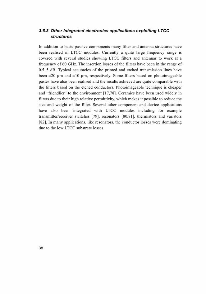
In addition to basic passive components many filter and antenna structures have been realised in LTCC modules. Currently a quite large frequency range is covered with several studies showing LTCC filters and antennas to work at a frequency of 60 GHz. The insertion losses of the filters have been in the range of 0.5–5 dB. Typical accuracies of the printed and etched transmission lines have been ±20 µm and ±10 µm, respectively. Some filters based on photoimageable pastes have also been realised and the results achieved are quite comparable with the filters based on the etched conductors. Photoimageable technique is cheaper and “friendlier” to the environment [17,78]. Ceramics have been used widely in filters due to their high relative permittivity, which makes it possible to reduce the size and weight of the filter. Several other component and device applications have also been integrated with LTCC modules including for example transmitter/receiver switches [79], resonators [80,81], thermistors and varistors [82]. In many applications, like resonators, the conductor losses were dominating due to the low LTCC substrate losses.

39
4 Experimental work
During the experimental work certain aspects of both gravure-offset-printing and LTCC technologies were developed in order to optimise them for the fabrication of passive components. Most of these components were intended for operating at frequencies below 2 GHz. At the outset of the present study it was recognized that more information concerning the various factors involved in the gravure-offset-printing process were needed. Most of the applications did not require very narrow conductors and, therefore, steel was the most suitable choice as a printing plate material due to its durability. However, there was a growing need to develop printing plates with high surface quality and engravings with good accuracy. After preliminary studies the research was mainly focused on brass and copper plates since their surface roughness was acceptable and, when necessary, could be further reduced by polishing.
The realisation of fine lines requires the use of appropriate inks. A survey of candidate inks was made at the outset of the study with suitability for gravure-offset-printing being the essential criterion. Paste rheology was varied by modifying the amounts and types of solvents to study their effects on electrical properties of the printed lines. In addition to ink development the effects of some printing pad properties, for example hardness and shape of the pad, and the machine speed were optimised for the specific applications.
Gravure-offset-printing was first developed using alumina substrates (Papers I and II) after which the process was transferred onto the LTCC. The miniaturisation of the passive components required the use of pastes having small particle sizes. During the work the kind of pastes designed for LTCC materials were not available and therefore the suitability of fine-line thick-film inks on LTCC materials was studied. Another important aspect in the miniaturisation was the mixture of high- and low-permittivity tapes to allow combining capacitive and inductive functions in the same component or module. These processes were verified by the design and fabrication of passive components, that is inductors (Paper III) and filters (Paper IV), based on the commercial tapes. Since resistors are essential components in the realisation of any RF module the issues related to their miniaturisation were also studied (Paper V). Screen-printing was used in the case of the printed resistors.
Because with the miniaturisation heat-management may become an issue this was also studied (Papers VI and VII). A novel idea was to modify the LTCC-M approach. This was realised by placing high- and low-permittivity tapes directly

40
on a thermally highly conductive heat sink. The tapes were then laminated and co-fired to form a compact module which also restricted shrinkage.
The experimental work described in Papers I–IV was carried out at the University of Oulu while that reported in Papers V–VII was conducted at VTT. The two different facilities involved some differences in the LTCC processing as described in detail below.
4.1 Gravure-offset-printing
Several materials, such as steel, copper, brass and polymers were tested as plate candidates; in preliminary experiments steel proved to be too difficult a material for making accurate engravings. Copper and brass resulted in the best quality so they were used in most of the experiments. The positive photosensitive resist was spread over the plates by the dipping method as the thickness of the resist layer was controlled by varying the lifting speed. The uniform resist layer of thickness of 2–3 µm was dried at 80 °C for 30 min followed by exposing through the mask at a wavelength of 380 nm for 20–30 s. Because of cost constraints emulsion–masking was adopted, rather than chromium-glass; this choice carried the penalty of poorer line edge accuracy. The exposed resist was developed in dilute sodium carbonate (Na2CO3) solution for about 1 min. The exposed plate was finally etched by sodium persulfate (Na2S2O8) at a temperature of 50 °C for 3–4 min. The depth of the engravings was controlled by the etching time. Typically the surface of brass plates was polished after resist removal in order to decrease the surface roughness.
The commercial polymer-based printing plates had an emulsion layer over which the mask was placed. The exposure time determined the depth of the engravings and the development was done by using water as a developing agent. The surface of the polymer plate proved to be too rough for fine-line printing. A XeCl excimer laser was also used to make engravings in the polymer plates. This removed the need for using any mask, however a drawback was that the time used to make a plate increased significantly.
Because the printing equipment was unsuited to roller-printing, pad-printing was used in most of the experiments. The printing pads, made from Dow – Corning Q3 series materials, consisted of a mixture of base material and catalyst. Entrapping of air was avoided during the mixing by stirring the composition in vacuum. The vacuum was maintained until the mixture was completely expanded

41
and returned to its original volume. Then, the mixture was poured into a mould and allowed to dry for 24 h at room temperature.
The pads used were relatively hard in order to reduce vibrations during printing and in this way the accuracy in the double-printing process was improved. Typically the hardness of the pads was from 10 to 18 Shore A. The shape was also varied, and tests proved that slightly rounded pads gave the most uniform printings.
The printing inks were commercial thick-film pastes, which were modified by adjusting their printing properties. In most cases the solvent was diethylene glycol diethyl ether which has an evaporation rate suited the clean room capability. The solvent was mixed with 5 to 10 weight-% ethyl cellulose which served as a binder. The most commonly used inks in the experiments were Ag and Au although Pt, Cu and resist inks were used in some instances. Ag was preferred due to its high conductivity meanwhile Au was used due to the ability to make pastes with small particle size. Cu requires a more complicated firing process to avoid oxidation, and Pt is an expensive metal.
The quality of the substrate surface is important in fine-line printings. Most of the printings were made on 96% alumina, but in some cases smoother substrates, such as 99.5% alumina or glass, were used. Because of relatively poor high temperature stability of the glass substrate it proved impossible to use the highly conductive pastes as in the case of the alumina substrates. Instead polymer silver pastes with lower firing temperature were used. Also other ceramic substrates, such as LTCC, were used in the experiments.
The printing machine, which was of the "open-cup" type, had a repetition accuracy of ±10 µm in the horizontal direction. The machine could be used with either rollers or pads, although less accuracy was achieved with the rollers. The limiting factor with the machine was the use of only small-sized pads and, therefore, the maximum size of the substrate was 5 × 5 cm2. By using rollers it was possible to print on slightly larger substrates. The ink could be spread over the plate manually or automatically, but for the present experiment a disadvantage of the automatic process was its demand for relatively large amounts of ink. Because of the lower ink demand, coupled with the ability to adjust the angle between blade and plate, the manual system was usually adopted. The printing speed was adjusted depending on the evaporation rate of the solvent in the ink.

42
4.2 Production of passive components
4.2.1 Simulation and design
The goal of the electrical simulations was to study the dependence of the electrical properties of passive components on the geometrical dimensions and material parameters. The simulations were made by the APLACTM circuit simulator which enables using individual iteration and integration strategies. APLAC is also suitable for high-frequency simulations where components based on different transmission lines are utilised [83]. In the case of planar inductors APLAC offers built-in models for microstrip inductors where a ground layer exists at a specified distance from the conductor layer.
A band-pass filter for LTCC was designed using the 3rd order Butterworth band-pass filter as a basis (Fig. 6(a)). This kind of structure is not a practical one to realise and hence it was slightly modified. For example, the series capacitance (C2) was divided into two capacitances C2a and C2b which were at both sides of the series inductor (L2) in order to eliminate the need of via holes from the inductor layer (Fig. 6(b)). Also, the inductances to the ground layer (L1 and L3) were removed in order to simplify the fabrication of the structure (Fig. 6(b)).
Fig. 6. a) A prototype Butterworth band-pass filter and b) a modified band-pass filter.
The compact filter was designed in three layers on the basis of this modified structure, shown in Fig. 7, where the node numbers correspond to the nodes in the equivalent circuit of the filter shown in Fig. 8. This equivalent circuit takes into account, for instance, capacitive parasitics caused by the small distance between the inductor and the ground layer.

43
Fig. 7. The structure of the filter consists of three layers. The dashed lines between different layers define via holes.
Fig. 8. The equivalent circuit of the filter in Fig 7.
The simulations showed that the inductance and resistance of the microstrip lines were small enough to be neglected from the modified equivalent circuit, shown in Fig. 9. The capacitances between the microstrip line and ground pattern have been combined and shown as a single capacitance between the nodes 1–0 and 4–0 in Fig. 9. The geometrical dimensions for the microstrip lines, capacitor electrodes and inductor were calculated and the values are shown in Table 2. There were also parasitic capacitances between the inductor and ground layers (C20 and C30). With these values the designed centre frequency of the filter in Fig. 9 was 1.25 GHz and the 3 dB bandwidth was less than 100 MHz.

44
Fig. 9. The simplified equivalent circuit of the filter in Fig. 7.
Table 2. The design values and dimensions of the components. The relative permittivity of the microstrip layer was 100.
Component Nodes Value Width [mm] Length [mm]
Microstrip C10=C40 2 pF 0.225 1.1
Series capacitor C12=C34 660 fF 1.0 1.0
Series inductor L23 22.5 nH 0.115 18.99
Parasitic capacitance C20=C30 1.4 pF
The ground and inductor layers were printed on a tape with a relative permittivity of 8 (ESL D-41010-70C), whereas the microstrip layer was printed on a sheet whose permittivity was 100 (ESL D-41210-C). The number of turns of the inductor was 2.5 and its size 2.7 × 2.7 mm2.
The resistors were designed to make them compatible with 0402 and 0201 size chip resistors. The main design parameter was the aspect ratio, i.e. the ratio of resistor length over width. It was varied from 0.43 to 8.2. The resistor widths were 250–1000 µm and the lengths 175–1435 µm.
4.2.2 Processing steps
Different commercial LTCC tape systems were used for inductors, filters and resistors. The inductors were realised on ESL D-41110-70C tape system with the relative permittivity of 4.2 and the loss tangent of 0.003. This tape group had the lowest permittivity commercially available at that time. The filters utilised the same tape added by the tape whose relative permittivity was 100. The resistors were printed on Du Pont 951 and Ferro A6-S tape systems.

45
The inductors were fabricated in a square shape to maximise the inductance value per unit area. Also, the fabrication design of the rectangular shape was easier in comparison with a circular shape. The maximum size of the inductor was 2.5 × 2.5 mm2. The line width of conductors varied from 60 to 175 µm. In addition to microstrip inductors, also inductors in one and two layers were fabricated. The layouts for the structure of each type of inductors are illustrated in Fig. 10.
(b) (c)(a)
Fig. 10. The layouts of (a) microstrip, (b) two-layer and (c) one-layer inductors. (Paper III).
The inductors and filters were processed at the University of Oulu. The processing was started by making via holes using both Nd-YAG and XeCl-excimer lasers, where punching was mainly used for making the registration marks. The diameter of the registration marks was 800 µm and that of via holes from 50 µm upwards. An advantage of the excimer laser was the possibility to make via holes without removing the supporting polymer film from the “green” sheet. In the case of Nd-YAG laser the polymer film had to be removed. Otherwise, the heat caused by the laser beam left some residues around the via hole.
Via holes were filled by screen-printing, after which the conductors were printed by the gravure-offset-printing method. The viscosity of the pastes was lowered by adding a mixture of solvents and binders. A double-printing method, that is drying between two conductor printings, was used in order to increase the thickness of the conductors. After printing, the conductors were dried at 100 °C for about 15 min in order to evaporate solvents.
The layers were aligned by the registration marks and the lamination performed at a temperature of 70 °C and a uniaxial pressure of 21 MPa for 15

46
min. Metal plates were set above and below the LTCC substrate to obtain an even pressure distribution. After lamination a visual inspection was used as a first check.
The firing of the inductors and filters was carried out in two ovens. During the study an oven dedicated for LTCC firing was not available at the University of Oulu. Therefore, the burn-out of the organic components was made at a chamber oven and the final firing in a conventional thick-film belt furnace consisting of four zones. The profile used is illustrated in Fig. 11. The profile does not take into account the temperature decrease of the samples during the transfer between the ovens. Finally, the individual samples were separated by scribing with the Nd-YAG laser. Silver paste terminations were applied to connect to the measuring equipment.
The fabrication of the band-pass filters followed essentially the same process as used for the inductors. The main difference was the use of commercial fine-line thick-film pastes, which were not designed to be shrinkage-matched with the LTCC materials. The purpose was to assess the possibility to realise smaller devices by decreasing the conductor line-width. The suitability of the fine-line ink on alumina was proved earlier (see chapter 4.1). Another difference was a combination of tapes having different permittivity values. In this way a significant reduction in the size of filters was possible.
The processing of resistors was carried out at VTT. The via holes were punched and filled by stencil-printing and the resistors were screen-printed. The lamination was made isostatically and the co-firing in a batch furnace dedicated to LTCC processing. The firing profiles for all tape systems are shown in Fig. 11. Some blank layers were placed under the resistor tape layer in order to give mechanical support for the structure. Typical temperature variation across the panel size of 19 × 19 cm2 was ±4 °C but in the vertical direction variation was only ±1 °C between different firing levels at the same horizontal locations.
The resistor pastes were CF-series for Du Pont 951 and FX87-series for Ferro A6-S tape systems. Both Du Pont and Ferro recommend using 325 mesh screens for resistor printing. However, it is not easy to realise small resistors with this kind of screen and therefore the experiments were made with a 400 mesh screen. The tolerance of resistance values is typically high with most LTCC foundries working to a tolerance of ±30%. This high tolerance can result from variation in printed thickness, firing conditions and effects of overglazes [84].

47
Fig. 11. The firing profiles for the various commercial tape systems: ESL ( ), Du Pont ( ), Ferro (Δ) and Heraeus (x) LTCC systems.
4.3 Heat-management development utilising zero-shrinkage LTCC systems
Some of the most critical problems in LTCC technology, i.e. shrinkage and heat management, were studied. The goal was to develop a method where LTCC “green” sheets were laminated directly on a heat sink and co-fired to form a modified LTCC-M structure. At the same time the electrical performance was enhanced by utilising tape system having mixed dielectric permittivities (εr). The method also allows an improvement in heat-management since high-power ICs can be placed on the heat sink through LTCC windows. The concept is illustrated in Fig. 12.
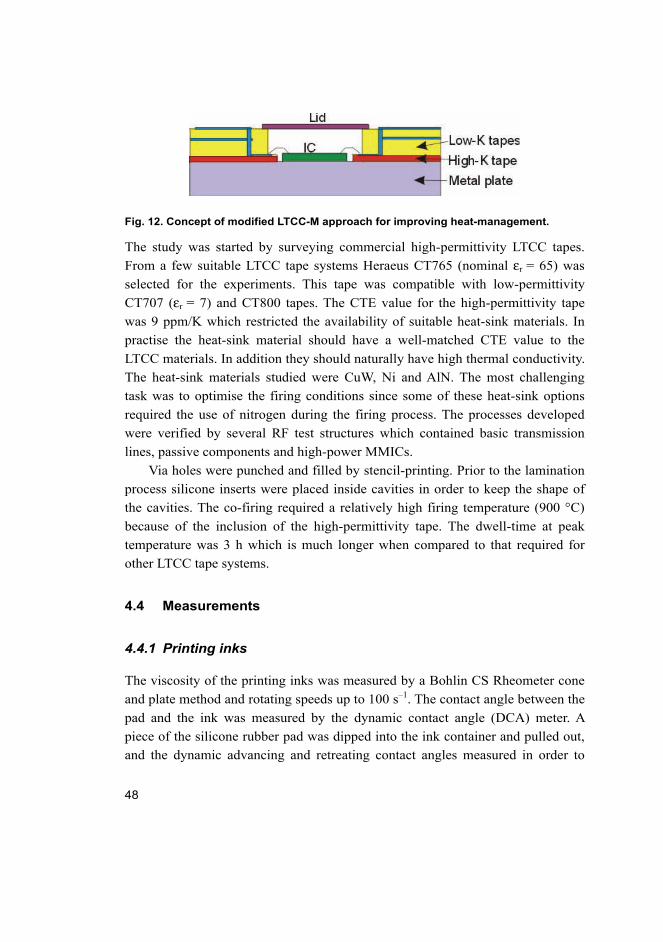
48
Fig. 12. Concept of modified LTCC-M approach for improving heat-management.
The study was started by surveying commercial high-permittivity LTCC tapes. From a few suitable LTCC tape systems Heraeus CT765 (nominal εr = 65) was selected for the experiments. This tape was compatible with low-permittivity CT707 (εr = 7) and CT800 tapes. The CTE value for the high-permittivity tape was 9 ppm/K which restricted the availability of suitable heat-sink materials. In practise the heat-sink material should have a well-matched CTE value to the LTCC materials. In addition they should naturally have high thermal conductivity. The heat-sink materials studied were CuW, Ni and AlN. The most challenging task was to optimise the firing conditions since some of these heat-sink options required the use of nitrogen during the firing process. The processes developed were verified by several RF test structures which contained basic transmission lines, passive components and high-power MMICs.
Via holes were punched and filled by stencil-printing. Prior to the lamination process silicone inserts were placed inside cavities in order to keep the shape of the cavities. The co-firing required a relatively high firing temperature (900 °C) because of the inclusion of the high-permittivity tape. The dwell-time at peak temperature was 3 h which is much longer when compared to that required for other LTCC tape systems.
4.4 Measurements
4.4.1 Printing inks
The viscosity of the printing inks was measured by a Bohlin CS Rheometer cone and plate method and rotating speeds up to 100 s–1. The contact angle between the pad and the ink was measured by the dynamic contact angle (DCA) meter. A piece of the silicone rubber pad was dipped into the ink container and pulled out, and the dynamic advancing and retreating contact angles measured in order to

49
determine the wetting properties and the adhesion of the ink to the substrate, respectively.
4.4.2 Test measurements for printed patterns
The dimensions of the conductor lines and dielectrics were measured using a surface profile meter (DEKTAK3ST) where a diamond stylus is drawn across the sample, and by a Wentforth profilemeter which is based on a capacitive measurement method. Scanning electron microscopy (SEM) was used to study cross-sections of the LTCC structures.
The adhesion of the ink to the substrate was measured using a “Sebastian Five” adhesion tester. In this a stud is glued to the conductor pad on the substrate and pulled until the stud and/or conductor is released. The force is continuously monitored during the process of the adhesive strength measurement.
4.4.3 Electrical measurements
The resistivity of the fine-line conductors was measured by the four-point method. The electrical characterisation of the inductors and filters was made by an LCR meter and a network analyser. The values of inductance and parasitic capacitance of the inductors were measured at a frequency of 20 Hz. The performance-dependence of the test structures on frequency was measured by the network analyser which was used up to 20 GHz. The measurements of the filters and resistors were made by probes, whereas the inductors required the use of holders designed for surface mount devices.

50

51
5 Results and discussion
5.1 The basics of gravure-offset-printing
5.1.1 Printing inks
The printing inks studied were commercial thick-film pastes. Due to the requirements of the gravure-offset-printing some solvents and binders were added to the pastes. The conditions of the working environment, for instance temperature and humidity, were taken into account in the selection of the solvent. The evaporation rate of the solvent was one of the key factors in the selection process of solvent. The function of the binder, such as ethyl cellulose, was to bind the metal particles together during the drying step.
The criteria in the selection of the inks to be studied were, for instance, electrical performance, suitability for processing and costs. After some preliminary experiments three inks were studied in more detail. Some of their basic properties are shown in Table 3. Au A ink was specially developed for fine-line printing whereas the others were normal thick-film pastes. The mean particle size of the fine-line ink (Au A) was below 1 µm. The distribution in the particle size should also be taken into account since larger particles can hinder the miniaturisation of the lines. All the pastes contained spherical particles. For the conductors the solids content should be as high as possible to maximise conductivity; unfortunately, in these experiments the solid content of the fine-line ink was quite low in comparison with that of the other inks. The particle size distribution and the viscosity were measured, whereas the square resistance and the solids content were obtained from the manufacturer's data sheets.
Table 3. Some properties of the pastes used in the experiments. The square resistance is given at a thickness of 1 µm.
Ink type Mean particle size
[µm]
Viscosity
(@10 s–1) [Pas]
Square resistance
[mΩ/ ]
Solid content
[%]
Ag A 3.53 150 Unknown 84
Au A 0.73 30 45–55 50–55
Au B 3.10 350 32 75
The viscosity of the as-received thick-film pastes (Ag A and Au B) was too high for gravure-offset-printing. Hence, it was reduced by adding a small amount (5–

52
15 wt. %) of a mixture of solvent and binder. The viscosity of the ink affected the broadening (relative variation of the line width on substrate vs. width of the engraving in the plate) and thickness of the conductor lines. As Paper I shows the broadening of the line decreased as the viscosity was increased. The minimum broadening of the conductor lines was about 10%. The thickness increased when the viscosity was increased up to a certain viscosity value. The transferability of the ink from the plate and the uniformity of the conductors degraded when the viscosity was too high.
A key parameter in the evaluation of the quality of conductor lines was the electrical resistivity. The square resistance of the conductor lines printed by the fine-line paste (Au A) did not change significantly as a function of viscosity whereas that for the normal thick-film paste (Au B) decreased when the viscosity was increased up to 60 Pas. The experiments showed that optimum printing characteristics required the viscosities of the inks to be individually adjusted. In this case, the optimal viscosity value was 30–40 Pas for the fine-line Au ink (Au A), 60 Pas for the thick-film Au ink (Au B) and 40 Pas for the thick-film Ag ink. For comparison, the viscosity of the screen-printing pastes before adding the solvents was over 100 Pas.
The measured resistivity values of the conductor lines printed by fine-line and conventional thick-film Au pastes respectively are shown in Table 4. It is seen that the values match well with each other. The adhesion of the gravure-offset-printed conductor lines was also close to that for the screen-printed conductor lines.
Table 4. Comparison of resistivities of Au lines.
Ink Square resistance
[mΩ/ ]
Thickness
[µm]
Resistivity
[10–8 Ωm]
Resistivity
[10–8 Ωm] from data sheets
Au A
(fine-line)
31 1.5 4.7 4.5–5.5
Au B (thick-film) 8 5.7 4.6 3.2
5.1.2 The effects of the printing plate on printing quality
Printing plates were fabricated by using chemical wet-etching and laser-processing. Wet-etching was a practical way to realise as narrow as 50 µm engraving. However, the main problem encountered was underetching, which limited the possibility to make very narrow engravings. On the other hand, the

53
excimer laser processing allowed narrow (<50 µm) engravings to be formed in the polymer plates. The laser was not a suitable tool in the case of the metal plates since the particles removed by the laser were of non-uniform sizes. The metal plates were polished after which the surface roughness of the metal plates was about 0.1 µm. In the case of too rough a surface, trapping of ink made the printing result very poorly defined leading to short-circuiting between the lines. The quality of the metal plates, especially brass, was better than that of the polymers. A further miniaturisation of the conductor lines requires the use of “additive” rather than “subtractive” printing plate manufacturing methods.
The effect of the engraving depth on line-width was studied by using two different depths, 18 and 26 µm. The broadening of the lines had no clear dependence on the depth of the engravings and this was also the case for the line-thickness of the fine-line ink. The line-thickness of the dried thick-film paste was 1 µm smaller when printed from the shallower engraving. Some experiments were also made with very deep engravings up to 50 µm. The thickness of the conductor lines still remained in the same range demonstrating that the thickness of the conductor lines can not be increased linearly as a function of the depth of the engravings. The ink on the bottom of the engravings did not dry quickly enough.
5.1.3 Other factors
The most important printing parameter defining the filling factor of the engraving was the angle between the doctor blade and the plate. The optimal value for the angle α in Fig. 2 was found to be 35–40°. Too low a value of α allowed the blade to rise up from the plate, whereas in the case of too high a value the engravings were not totally filled by the ink.
The surface roughness Ra (the area between the profile line and its mean line over the evaluation length) of the substrates was measured by DEKTAK3ST and it also affected the printing process. The surface roughness of commercial 96% alumina substrates is about 1.3 µm and this was small enough to allow printing of thick-film pastes. However, the thickness of conductors printed using organometallic inks was only of order 10–7 m and, hence, a smoother substrate surface is required. For these inks, commercial 99.5% alumina substrates had to be used.
Several shapes of silicone rubber pads were tested. When the surface of the pad was totally flat, many voids appeared in the printed pattern. This was due to

54
air pockets trapped between the pad and substrate; a slightly rounded surface avoided this problem. On the other hand, strongly curved pads increased the amount of distortion in printed conductor lines. With too soft a pad (below 10 Shore A) the adhesion of the ink to the pad was too strong so that not all the ink was released to the substrate. With too hard a pad (above 18 Shore A) the printed area was too small.
Gravure-offset-printing was used to fabricate, for instance, sensors, lumped passive components and transmission lines. Some of these devices operated at high frequencies where good printing accuracy was an essential feature. The width of conductor lines was measured over the conductors on several locations by DEKTAK3ST. The variation in line width was about ±5% for 100 µm wide lines. The narrowest conductor lines printed in this study were about 30 µm wide. In addition, the surface roughness of the conductors was smaller in comparison with screen-printed conductors. These results are comparable with those obtained for conductors fabricated by photoimaging methods. However, due to the additive character of the gravure-offset-printing, the waste of conductor material is smaller in comparison with photoimaging methods.
The gravure-offset-printing proved to be a suitable method for printing narrow conductors on various substrates. The main advantage when compared with other fine-line thick-film technologies is the possibility to print on non-planar surfaces due to the flexible printing pad.
The implementation of the gravure-offset-printing into a wider use in electronics production needs further development of several aspects. In most machines, the pad is moving horizontally and this can reduce printing accuracy due to the vibration of the pad during the movement. Some improvement could be achieved with the plate moving rather than the pad. Another serious problem encountered during the study was a lack of suitable commercial conductive inks for fine-line printing. The inks to be used in the gravure-offset-printing need to be tailored depending on specific conditions. Inks with a small particle size need also correct solvents so that the drying rates and the speed of the printing machine are well matched.
5.2 Gravure-offset-printing inks for LTCC tapes
Typically, LTCC tapes require special inks for which their shrinkage is matched to that of the tapes during firing. However, these inks are not usually designed for

55
fine-line printing and so the use of a fine-line thick-film paste would be an interesting option, as reported in Paper IV.
Both a special shrinkage-matched LTCC-compatible paste and a normal thick-film paste were printed on unfired LTCC tapes by gravure-offset-printing. The amount of the mixture of organic solvent and binder added to the shrinkage-matched paste was in the range 5–10 wt %. The viscosity of the ink was approximately 20 Pas at a shear rate of 20 s–1. Printing of narrow conductor lines (<75 µm) with this paste was difficult due to the large particle size (average size 5 µm). The smaller particle size of the fine-line paste (average size 1.1 µm) made it possible to print lines down to a width of 50 µm. The shrinkage varied depending on the tapes and inks. The horizontal shrinkages of the conductor lines printed by the fine-line and shrinkage-matched inks were 6.5% and 5.7%, respectively. The shrinkages of the three different tapes (Du Pont 943, ESL 41010 and Du Pont 951) were 11.3, 12.0 and 13.4%, respectively.
Table 5 shows resistivity values of conductors printed with three different inks on two different LTCC tapes. The determination of the exact resistivity value was difficult, to some extent, due to large thickness variations. The resistivity values of the conductors in Table 5 are based on average thickness values and the values given by the manufacturers are also shown, for comparison. In most cases the measured resistivity is slightly higher than the manufacturer’s value. However, a combination of a fine-line thick-film ink and an unfired LTCC tape proved to be feasible for gravure-offset-printing of conductors.
The use of gravure-offset-printing together with LTCC materials is an interesting route, the main problem encountered being adhesion between the printing pad and green sheet. The printing table had to be modified so that there was sufficient “vacuum suction” to prevent the tape being lifted by the pad.
Table 5. Measured resistivity values of LTCC conductors printed by gravure-offset-printing with a fine-line thick-film ink and two shrinkage-matched inks on two different tapes. Resistivity values given by the ink manufacturers are also shown.
Ink Tape Resistivity
[10–8 Ωm]
Resistivity given by manufacturer
[10–8 Ωm]
D-8881-B Du Pont 943 5.2 1.8–3.6
D-8881-B ESL 41010 2.4 1.8–3.6
HF602 Du Pont 943 4.6 2.4–2.9
D-901-CT ESL 41010 4.6 3.6

56
5.3 Study of planar inductors
5.3.1 Computer simulations
The effects of different parameters on the electrical performance of planar inductors were studied using computer simulations. The variables studied were the size of the inductor, the ratio of the line width to their separation, the number of conductor turns, the distance between the ground and the inductor layer, the thickness and the resistivity of the conductor, and the permittivity and loss tangent of the substrate.
In the simulations, the effect of each parameter was studied separately by fixing the other parameters. The fixed parameter values used in the simulations were typical for the fabricated inductors. The size of the inductor was 2.5 × 2.5 mm2, the line width/space 100/100 µm and the number of turns 4.5. The thickness of the conductor and substrate was 6 and 400 µm, respectively, and the relative permittivity and loss tangent of the substrate were 4.2 and 0.003, respectively. The conductivity of the conductor was 70% of the conductivity of pure gold, which was used as a reference in the APLAC simulator software.
The values of inductance and parasitic capacitance increased linearly when the side length of the square inductor was increased. The effect of the line width/space values was studied by using two different pitches, 250 and 200 µm, while the line width was varied from 70 to 130 µm. The corresponding results are given in Paper III. The inductance decreased slightly when the line-width increased whereas the capacitance behaved in the opposite sense. By changing the pitch from 250 to 200 µm, while keeping the line-width constant, the inductance increased significantly. As the number of turns was increased the inductance increased non-linearly. An increase in substrate thickness increased the inductance and decreased the capacitance values; the relative permittivity of the substrate did not affect the inductance but only the capacitance values. The thickness and the resistivity of the conductor had no significant effect on the electrical properties.
5.3.2 Planar inductors integrated into a LTCC module
The line-width of the conductors was limited to a minimum of 60 µm due to the large particle size of the shrinkage-matched LTCC paste. A typical variation of the line-width was ±10%. During firing the LTCC substrate shrank 13% in the surface direction and 18% in thickness. The small areal changes in the conductor

57
patterns due to shrinkage were ignored. The resistivity of the conductor was 3.6x10⁻⁸ Ωm.
The measured inductance values of the circular one-layer inductors were lower in comparison with the square ones of similar size (1.7 × 1.7 mm2). The circular inductors were also more difficult to print. If the engravings were parallel to the blade a part of the ink was pulled out from the engravings onto the surface of the plate. This increased the risk of short-circuiting of the inductors. The measured inductance value of the circular inductors with 3 turns and the line width/space value of 125/140 µm was 7.0 nH compared to the calculated value of 10 nH. The highest inductance values for 2.5 × 2.5 mm2 size inductors were about 70 nH when the number of turns was 6.5 and the line width 75 µm. These inductors had Q-values of about 25 at a frequency of 1 GHz.
For the microstrip inductors the effects of the ground-layer and the conductor line-pitch were studied. The inductance decreased when the distance between the ground and conductor layers decreased, as predicted by the simulation. The simulated inductance values of the microstrip inductors were much smaller than the measured ones. The simulation model does not take into account variations in the width and thickness of the conductors. Also, the measurement system might cause some extra losses.
The same layout was also used for two-layer inductors. After firing the thickness of the two-layer inductor was 360 µm and the areal size 2.5 × 2.5 mm2. The variation of the inductance and resonant-frequency values was ±10%. The resonant frequencies were rather low, lower than 0.6 GHz, due to the parasitic capacitance between the layers.
A direct comparison of the properties of inductors fabricated by different methods is difficult due to varying geometries and dimensions reported in the literature. The Q-factor of inductors formed on a silicon chip is usually quite low, typically less than 5 at 1 GHz. Further disadvantage is the waste of valuable die surface area [85]. Better results have been obtained with MCM technologies. In MCM-D, Q-factors up to 17 have been realised with inductance values up to 34 nH at a frequency of 1.5 GHz [86,87]. Inductors have been also realised in MCM-L structures. Similar inductance and quality-factor values with the inductors fabricated in this study were achieved, but the size of the inductors was larger [88].

58
5.4 Study of filters
5.4.1 Computer simulations
The APLAC computer simulations showed that the inductance and resistance values of the microstrip lines had a negligible effect on the characteristics of the band-pass filter. The equivalent circuit of the lumped-element filter is shown in Fig. 9. The series inductance (L23) and the parasitic capacitances between the inductor and ground plane (C20 and C30) had the strongest effect on filter performance. The tolerance of the parameter values should be kept within 2% in order not to affect the centre frequency of the pass-band. Also the series capacitances (C12 and C34) and the parasitic mutual capacitance of the inductor turns (C23) had an effect on the pass-band.
5.4.2 Fabrication
The line-width of the fired thick-film conductors in the inductor pattern was 100 µm ± 10%. The average horizontal shrinkage of the LTCC substrate during firing was 12% and the thickness shrinkage 18%. The surface roughness (Ra) was less than 1.5 µm when only low-permittivity (εr = 4.2) sheets were used. When a high-permittivity (εr = 100) sheet was embedded between the low-permittivity sheets the surface roughness of the module and the warpage of the substrate slightly increased. However, there was no deformation between the tape layers. Also the misalignment between the layers was small, of approximately 20 µm. This kind of matching of different tapes is a requirement for an effective miniaturisation of the filters.
In the use of conventional thick-film pastes on LTCC tapes some problems were encountered. In spite of the presence of some voids in the filled vias an acceptable conductivity was achieved. The conductors shrank slightly more than the conductors printed with the shrinkage-matched pastes. A low solid content in the paste was the main drawback with the technique since it caused low fired line thicknesses (from 1 to 3 µm) and, hence higher square resistances.
5.4.3 Electrical performance of filters
The inductance value of the series inductor was between 21.5 and 23.9 nH. The transmission parameters of the band-pass filter at frequencies from 1.1 to 1.3 GHz

59
are shown in Fig. 13. The centre frequency of the filters is 1.20 GHz ± 0.01 GHz with a low attenuation, while the design centre frequency was 1.25 GHz. The 3 dB bandwidth is 52 MHz resulting in a Q-factor value of 23. The simulation results of the same filter based on the equivalent circuit in Fig. 9 are also shown in Fig. 13, for comparison.
Fig. 13. Measured (- -) and simulated (- -) attenuation of the 1.2 GHz band-pass filter as a function of frequency.
5.4.4 Comparison between simulated and measured values
The measured transmission parameters were used as target data for the simulator in order to determine the actual component values. The results for the 3rd order band-pass filter with the centre frequency of 1.2 GHz are shown in Table 6, where some calculated (C10, C40, C12, C34) and measured (C23, L23) values are also shown, for comparison. The components are the same as in Fig. 9. The parameter values of L23 and C23 were obtained from the LCR meter measurements and they were used as initial values in the simulation. The simulation results matched quite well with the calculated component values in Table 6.
The simulations showed that the series capacitance was one of the most important components to affect the sensitivity of the centre frequency of the band-pass filter. Misalignment of the tape layers and shrinkage variations caused the variation of the series capacitance values. Typical misalignment inside an LTCC module was approximately 20 µm, which corresponds to a difference of ~4 fF in

60
the capacitance value, when εr = 100 and the distance between the capacitor plates 80 µm. The horizontal shrinkage variation was ±1% around the average value. The variations of the inductance, capacitance and resonant-frequency values and conductor line widths were ±10%. However, the simulations together with experimental results showed that it is possible to realise a lumped-element-based filter in an LTCC module with low attenuation in the UHF range. Also, by combining layers with different permittivity values it was possible to realise a high capacitance value in a small area and hence decrease the size of the filter.
Table 6. Calculated (C10, C40, C12, C34), measured (C23, L23) and simulated component values of the 3rd order filter with the centre frequency of 1.2 GHz.
Component Calculated/Measured Simulated
C10=C40 2.0 pF 1.86 pF
C12=C34 0.645 pF 0.606 pF
C23 0.02 pF 0.02 pF
L23 22.5 nH 22.7 nH
5.5 Study of resistors
The thickness of dried resistors was measured by using a capacitive profile meter. There were some differences in the thickness between large and small resistors. For example, the mean thickness of 1000 µm wide and 475 µm long unfired CF031 Du Pont resistors was 10.3 µm, whereas the value was 13.9 µm for 250 µm wide and 350 µm long resistors. Du Pont recommends the unfired thickness of resistors to be 18–22 µm. The lower thickness value was due to the high-mesh-count screen used in the printing. Repeatability is an important issue in production and this proved to be good since the difference in the thickness values between modules was quite small, in the range of 1–2 µm.
The DC resistance was measured using a general-purpose resistance meter. In the case of Du Pont resistors, the resistance values printed with 10 Ω/ paste were quite high and higher than the design values, the difference depending on the geometrical size of the resistor. The measured square resistances for 100 Ω/ pastes were about half of the design values and in this case the ratio did not depend on the geometrical size of the resistors. The average tolerance of the resistance values was <±8%.
In the case of Ferro resistors the measured resistance values were much higher than the design value. However, in this case the difference between the

61
measured and design values did not depend on the geometrical size of the resistors. Also the tolerance of the square resistance values was very small, <±3.5% for the 10 and 100 Ω/ pastes, whereas it was higher, ±12%, for the 1 kΩ/ paste.
The resistance values are sensitive to environmental effects. The resistors can be protected by a glass paste overlay. The glass paste can also be used for tuning the resistance values.
5.6 Heat-management in the case of LTCC-M approach
The lamination and co-firing of Heraeus high- and low-permittivity tapes was first tested on a CuW heat-sink. Unfortunately, this material requires a reducing atmosphere during firing. It proved to be too difficult to control the firing conditions reliably and with acceptable repeatability. Nickel was easier to work with, but also in this case repeatability proved to be a challenge. AlN was the best option for this case. Due to a large CTE mismatch between the high-permittivity tape and AlN it was not possible to attach tapes directly to AlN. Cracks appeared on the tape after firing. However, when Au was deposited on an AlN layer, the situation improved significantly. It was then possible to attach both high- and low-permittivity tapes to AlN without cracks; the adhesion of the tapes to Au-plated AlN was also good.
This kind of an LTCC-M approach restricts the natural shrinkage of LTCC tapes and pastes. Since the pastes were not designed for non-shrinkage systems, some problems occurred due to the incompatibility between the paste and tape, especially in the case of the vias. Another problem was encountered with the dielectric. The capacitance measurements showed that the relative permittivity of the dielectric was only approximately 45 instead of 65 which is the value obtained for the dielectric under normal, free-shrinkage conditions. Due to this restricted shrinkage there may be more pores inside the dielectric lowering its relative permittivity.

62

63
6 Summary and suggestions for future work
The thesis describes the development of the gravure-offset-printing technique for application to fine-line printing. The technique was utilised in the fabrication of passive components in low-temperature co-fired ceramic (LTCC) modules. LTCC technology was further developed by utilising the modified LTCC-M approach for improving heat-management.
The most important variables in the gravure-offset-printing technique are printing-inks, plates, printing parameters and pads. Printing-inks were developed by adjusting the amount of solvents and binders in order to finely tailor the viscosity of the ink. Both conventional and fine-line thick-film pastes were tested. The manufacturer’s quoted resistance values of both conductor types were close to the values obtained by the screen-printing technique. The dimensions of the printed lines were measured as a function of viscosity. By increasing the viscosity the broadening of the lines decreased and their thickness increased. In this way, an optimal viscosity range for each ink could be determined.
Chemical wet-etching proved to be the fastest method for engraving the printing plates, but underetching limited the production of very narrow engravings. It was observed that by increasing the depth of the engravings it was not possible to increase the thickness of the conductor lines in a linear manner. Of the printing machine settings the angle between blade and plate was critical in maximising the fill of the engravings with ink.
Gravure-offset-printing was also used for printing on unfired LTCC tapes, in addition to normal alumina substrates. The problems caused by the shrinkage mismatch between the tapes and conductor lines were challenging. It was found that normal fine-line thick-film pastes could be printed on unfired LTCC tapes, although there was a shrinkage difference between the paste and tape. However, the shrinkage difference between a special LTCC ink and conventional thick-film paste was insignificant.
Several test-structures of passive components were fabricated during the study. A computer simulation of planar inductors enabled the effects of different parameters on the electrical performance of the inductors to be determined. A microstrip inductor was used in the simulation since the circuit simulator offered a built-in model for this kind of structure. The most important parameters were found to be the inductor size and number of turns in the inductor.
Microstrip inductors were then realised in addition to one- and two-layer inductors. The ground layer beneath the inductor layer decreased the self-resonant

64
frequency of the inductor. Therefore, other structures were also fabricated. One-layer inductors allowed a realisation of higher resonant frequencies with corresponding rather low inductance values; in the case of two-layer inductors a higher achieved inductance resulted in a low resonant frequency.
The band-pass filters were also computer-modelled before the manufacturing phase. A prototype Butterworth filter was used as a basis but modified in order to simplify the manufacturing process. The computer simulation defined the geometrical dimensions of the filter. Some of the filters were manufactured in LTCC modules where the relative permittivity of the tapes varied from layer to layer. The layers matched well with each other during the firing phase. The inclusion of the high-permittivity tape allowed a reduction in the size of capacitors needed in filter structures. The centre frequency of the fabricated filters matched well with the design value at the low UHF range. When the frequency was increased the attenuation of the lumped-element filters also increased.
The small-size printed resistors showed that good tolerances of square resistance values, <±12%, can be achieved by optimising the printing and firing conditions. The smallest resistors had a size of 250 × 350 µm2. With the best pastes the dependence of the measured vs. designed square resistance on the size of the resistors was negligible. Generally it was difficult to achieve a very good match between the designed and measured resistance values.
The modified LTCC-M approach was based on exploiting AlN as a heat-sink and on a mixture of high- and low-permittivity tapes. By optimising processing, for example, firing profiles, it was possible to attach these tapes over the heat-sink and achieve flat and well-adhered structures. The heat-generating chip could now be attached directly to a heat sink through LTCC cavities. The electrical characterisation demonstrated that the concept is working although the compatibility of the pastes and tapes should be further improved.
The study has demonstrated that the gravure-offset-printing process can be successfully adopted for the fabrication of passive components on LTCC. There are several issues to be developed. During the study the availability of commercial conductor inks suitable for gravure offset printing was poor. The utilisation of the gravure-offset-printing process for electronics manufacturing requires a tight collaboration within ink manufacturers, equipment manufacturers (including printing machines and silicone rubber pads/rollers), and end-users. The industrial process requires high-speed printing which on the other hand sets requirements for the drying speed of solvents in the inks. Thick enough conductor

65
lines should be achieved with a single print instead of multiple prints used in the present study.
Materials development is also needed for the LTCC pastes. It was seen that there were some problems with the quality of filled vias due to the constrained sintering. For adapting developed methods shrinkage-matched pastes need to be also developed. In this case the development work requires also collaboration between the paste manufacturer and process developer.

66

67
References 1. Haskard MR (1988) Thick-Film Hybrids. Prentice Hall, New York. 2. Dziedzic A, Nijs J & Szlufcik J (1993) Thick-film fine-line fabrication techniques -
application to front metallisation of solar cells. Hybrid Circuits 30: 18–26. 3. Barnwell P & Wood J (1997) A novel thick film on ceramic MCM technology
offering MCM-D performance. Proc. International Conference on Multichip Modules, Denver, USA: 48–52.
4. Carr B (1993) An introduction to thick film fine line printing screens. Proc. 9th European Hybrid Microelectronics Conference, Nice, France, 123–133.
5. Robertson C, Shipton RD & Gray DR (1999) Miniature sensors using high density screen printing. Sensor Review 19(1): 33–36.
6. Minalgine J, Baltrushaitis V & Muckett S (1994) Very fine line photoimageable thick film - process & applications. Proc. International Conference on Electronics Technologies, Windsor, United Kingdom, 49–55.
7. Savage D, Stewart TI & Zeniya Y (1989) Ultra fine line thick film golds using photolithographic techniques. Hybrid Circuit Technology 6(9): 56–58.
8. Teng K & Karim A (1989) Thick film electrostatic printing. Proc. 39th Electronic Components Conference, Houston, USA, 681–688.
9. Zeng X, Li X, Liu J & Qi X (2006) Direct fabrication of electronic components on insulated boards by laser microcladding electronic pastes. IEEE T on Advanced Packaging, Vol. 29, No. 2, May 2006, 291–294.
10. Shimada M, Watanabe H, Tsukamoto M & Ishida T (1990) Manufacturing of fine-line films by printing technique. Proc. IMC 1990, Tokyo, Japan, 581–585.
11. Lehn B (1984) The pad-printing process - an outline for plastics manufacturers. Swiss Plastics 6(7–8): 23–30.
12. Nakao K, Hayama M, Kuramasu K, Shimada M & Tsukamoto M (1991) Giant micro-electronics technology using gravure printing techniques. Proc. International Conference on Solid State Devices and Materials, Yokohama, Japan, 599-601.
13. Love GR, Maher G & Lambrecht RA (1997) Pad printer. Proc. Electronic Components and Technology, San Jose, CA, 972–978.
14. Mizuno K & Okazaki S (1991) Printing color filter for active matrix liquid-crystal display color filter. Japanese Journal of Applied Physics 30(11B): 3313–3317.
15. Eustice AL, Horowitz SJ, Travis AR & Nishii N (1986) Low temperature co-fireable ceramics for multilayer interconnect hybrids. Proc. IMC, Kobe, Japan, 49–60.
16. Vitriol WA & Steinberg JI (1983) Development of a low temperature cofired multilayer ceramic technology. International Journal of Microelectronics: 593–598.
17. Wilcox DL, Huang RF & Kommrusch R (1999) The multilayer ceramic integrated circuit (MCIC) technology: an enabler for the integration of wireless radio functions. Advancing Microelectronics July/August: 15–20.
18. Brown RL & Smith WR (1997) Embedded passive functions for RF and mixed-signal circuits. Proc. International Conference on Multichip Modules, Denver, USA, 351–356.

68
19. Nishikawa H, Tasaki M, Nakatani S, Hakotani Y & Itagaki M (1993) Development of zero x-y shrinkage sintered ceramic substrate. Proc. Japan International Electronic Manufacturing Technology Symposium, Kanazawa, Japan: 238–241.
20. Reed R (1955) Offset Platemaking, Deep-Etch. Lithographic Technical Foundation, Inc., New York.
21. Kiddell P (1994) Padprinting: controlling ambient conditions for better quality. Screen Printing July: 94–97.
22. Bery YA (1985) Mechanisms governing gravure printing. Proc. Coating Conference, Atlanta, GA, 149–159.
23. Xiao HH (1984) Laser technology application in gravure offset printing. Proc. SPIE - The International Society for Optical Engineering, 2118: 209–212.
24. Leppävuori S, Väänänen J, Lahti M, Kukkola K & Uusimäki A (1994) The use of gravure offset printing in the realisation of fine line thick film conductors. Proc. MRS Symp., Boston, USA, 323: 85–90.
25. Blasche DW (1993) Methods of cylinder engraving for gravure printing. TAPPI Journal August: 169–174.
26. Mikami Y, Nagae Y, Mori Y, Kuwabara K, Saito T, Hayama H, Asada H, Akimoto Y, Kobayashi M, Okazaki S, Asaka K, Matsui H, Nakamura K & Kaneko E (1994) A new patterning process concept for large-area transistor circuit fabrication without using an optical mask aligner. IEEE Transactions on Electron Devices 41(3): 306–314.
27. Bassemir RW & Krishnan R (1990) Practical applications of surface energy measurements in flexography. FLEXO July.
28. Sjöling B, Turvey SP & Alexander JH (1994) Design and processing considerations for the use of a crystallising low temperature cofiring ceramic tape system with integratable passive components. Hybrid Circuits 34: 48–51.
29. Chang CR & Jean JH (1999) Crystallization kinetics and mechanism of low-dielectric, low-temperature, cofireable CaO-B2O3-SiO2 glass-ceramics. Journal of the American Ceramic Society 82(7): 1725–1732.
30. Block C., Hagn P, Hoffmann C, Korden C & Ruppel C (2006) LTCC technology for system in package solutions. Topical meeting on Silicon Monolithic Integrated Circuits in RF Systems 2006, 237–240.
31. Wang G, Folk E, Barlow F & Elshabini A (2006) Fabrication of microvias for multilayer LTCC substrates. IEEE T on Electronics packaging manufacturing, Vol. 29, No. 1, 32–41.
32. Muller J, Perrone R, Thust H, Drue KH, Kutscher C, Stephan R, Trabert J, Hein M, Schwanke D, Pohlner D, Reppe G, Kulke R, Uhlig P, Jacob AF, Baras T & Molke A (2006) Technology benchmarking of high resolution structures on LTCC for microwave circuits. Proc. Electronics Systemintegration Technology, Dresden, Germany, 111–117.
33. Taguchi Y, Miyauchi K, Eda K & Ishida T (1993) A GHz-band ceramic multi-layer substrate and its application to a hybrid IC. IEEE MTT-S Digest Proceedings 1325–1328.

69
34. Muller J, Schwanke D, Gerdes J, Haas T, Josip D & Klein J (1998) Improved manufacturability and yield by changing the relationship between cofire and postfire steps in LTCC. 43rd International Scientific Colloquium, Ilmenau, Germany, 128–133.
35. Bauer R, Golonka LJ, Kirchner T, Nitsch K & Thust H (1998) Optimization of thermal distribution in ceramics and LTCC structures applied to sensor elements. Microelectronics International 15(2): 34–38.
36. Kawakami K, Takabatake M, Minowa T, Chiba J & Sasaki M (1986) A low-temperature cofired multilayer ceramic substrate. In: Blum JB & Cannon WR (eds) Advances in Ceramics 19: Multilayer Ceramic Devices. The American Ceramic Society Inc, Westerville: 95–102.
37. Kniajer G, Dechant K & Apté P (1997) Low loss, low temperature co-fired ceramic with medium dielectric constants. International Journal of Microcircuits & Electronics Packages 20(3): 246–253.
38. Thust H, Drüe KH, Müller J, Thelemann T, Tuschick R, Chilo J, Golovanov C & Ndagijimana F (1998) Coupling behaviour between transmission lines with meshed ground planes in LTCC-MCMs. Microwave Journal 41(11): 70–79.
39. Kumar AH, Knickerbocker S & Tummala RR (1992) Sinterable glass-ceramics for high-performance substrates. IEEE Proceedings 672–681.
40. Kondo K, Okuyama M & Shibata Y (1986) Low firing temperature ceramic material for multilayer ceramic substrates. In: Blum JB & Cannon WR (eds) Advances in Ceramics 19: Multilayer Ceramic Devices. The American Ceramic Society, Inc., Westerville, p 77–87.
41. Pruna P, Gardner RD, Hankey DL & Turvey SP (1998) Microwave characterization of low temperature cofired ceramic. Proc. International Symposium on Advanced Packaging Materials, Braseltown, USA, 134–137.
42. Jantunen H, Rautionaho R, Uusimäki A & Leppävuori S (2000) Preparing low-loss LTCC material without glass addition. Journal of the American Ceramic Society, 83(11): 2855–2857.
43. Dziedzic A. Golonka LJ & Henke M (1998) Temperature properties of low temperature cofiring ceramics (LTCC) and multilayer capacitors. 43rd International Scientific Colloquium, Ilmenau, Germany, 198–202.
44. Kata K & Shimada Y (1992) Low dielectric constant multilayer glass-ceramic substrate controlled isolated porosity. NEC Research & Development 33(2): 133–144.
45. Kellerman D, Nabatian DJ, Bokalo P, He F, Retherford L, Barlow F & Elshabini A (1998) Characterization and processing of low dielectric constant thick film substrates for electronic packaging applications. Proc. International Symposium on Advanced Packaging Materials, Braseltown, USA, 130–133.
46. Jaakola T, Kautio K, Petäjä J & Lenkkeri J (2003) Thermal management of power MMIC on LTCC substrate. Proc. 14th European Microelectronics and Packaging Conference and Exhibition, Friedrichshafen, Germany, 86–91.
47. Kinzy Jones W, Liu Y & Gao M (2003) Micro heat pipes in low temperature cofire ceramic (LTCC) substrates. IEEE T on Components and Packaging Technologies, Vol. 26, No. 1, 110–115.

70
48. Fathy A, Pendrick V, Ayers G, Geller B, Narayan Y, Thaler B, Chen HD, Liberatore MJ, Prokop J, Choi KL & Swaminathan M (1998) Design of embedded passive components in low temperature cofired ceramic on metal (LTCC-M) technology. Proc. IEEE MTT-S, Vol. 3, 1281–1284.
49. Drüe KH, Thust H & Müller J (1999) RF models of passive LTCC components in the lower Gigahertz-range. Applied Microwave & Wireless 11(10): 26–35.
50. Shim KB, Cho NT & Lee SW (2000) Silver diffusion and microstructure in LTCC multilayer couplers for high frequency applications. Journal of Materials Science 35: 813–820.
51. Page JP, Amey DI, Draudt R, Horowitz SJ, Polzer E, Cicognani J & Kojo H (1999) Cost trade-offs of constrained sintering of low temperature cofired ceramic. Proc. IMAPS - Europe, Harrogate, United Kingdom.
52. Hintz M, Thust H & Polzer E (2002) Generic investigation on 0-shrinkage processed LTCC. Proc IMAPS Nordic, Stockholm, Sweden, 243–249.
53. Barnwell P, Amaya E, Lautzenhiser F & Wood J (2002) HeralockTM 2000 Self-constrained LTCC tape - benefits and applications. Proc. IMAPS Nordic, Stockholm, Sweden, 250–256.
54. Dispenza M, Buttiglione R, Fiorella AM, Tuominen J, Kautio K, Ollila J, Korhonen P, Lahdes M, Rönkä K, Catoni S, Pochesci D, Marcelli R, Foglietti V, Cianci E & Coppa A (2007) Fabrication of high performance RF-MEMS structures on surface planarised LTCC substrates. Proc. EMPC, Oulu, Finland, 369–374.
55. Nelson C, Sigliano R & Makihara C (1997) Built-in passive components in multilayer ceramics for wireless applications. Proc. International Symposium on Advanced Packaging Materials, Braselton, USA, 75–80.
56. Delaney K, Barrett J, Barton J & Doyle R (1998) Characterisation of the electrical performance of buried capacitors and resistors in low temperature co-fired (LTCC) ceramic. Proc. Electronic Components and Technology Conference, Seattle, USA, 900–908.
57. Tsukamoto S, Kanda A & Taga S (1999) Multilayer glass-ceramic substrate and RF circuit design technology for mobile communication components. Proc. IMAPS - Europe, Harrogate, United Kingdom.
58. Amey D, Barnwell P, Brown R, Gaughan F, Horowitz S, London A, Novak R, Slutz D & Wilcox D (1999) Ceramic solutions for cost savings in handsets. Proc. IMAPS- Europe, Harrowgate, United Kingdom.
59. Rector J, Dougherty J, Brown V, Galvagni J & Prymak J (1997) Integrated and integral passive components: a technology roadmap. Proc. Electronic Components and Technology Conference, San Jose, USA, 713–723.
60. Arbuckle B, Logan E & Pedder D (2000) Processing technology for integrated passive devices. Solid State Technology November: 84–90.
61. Xiao AY, Tong QK & Savoca AC (1999) Polymer thick film materials for integral resistors. Proc. Electronic Components and Technology Conference, San Diego, USA.

71
62. Ramesh S, Huang C, Liang S & Giannelis EP (1999) Integrated thin film capacitors: interfacial control and implications on fabrication and performance. Proc. Electronic Components and Technology Conference, San Diego, USA.
63. Frye RC (1996) Passive components in electronic applications: requirements and prospects for integration. International Journal of Microcircuits and Electronic Packaging 19(4): 483–489.
64. Benson DC, Xuan Y, He J, Lin CM, Hodges CR & Logan EA (1997) Integrated passive components for RF applications. Proc. Wireless Communications Conference, Boulder, USA, 175–180.
65. Breen B (1991) Multi-layer inductor for high frequency applications. Proc. Electronic Components and Technology Conference, Atlanta, GA, 551–554.
66. O'Reilly S, Duffy M, O'Donnell T, Mathuna SC, Scott M, Young N & Payne S (1999) Integration of a range of RF chip inductors in advanced printed circuit board technology. Proc. IMAPS - Europe, Harrogate, United Kingdom, 363–369.
67. Kawabe K, Koyama H & Shirae K (1984) Planar inductor. IEEE Transactions on Magnetics 20(5): 1804–1806.
68. Barnwell G & Tucker CE (1973) The radio frequency properties of thick film components. Proc. Hybrid Microelectronics Conference, Canterbury, United Kingdom, 175–190.
69. Gupta KC, Garg R & Chadha R (1981) Computer-Aided Design of Microwave Circuits. Artech House, Inc., Norwood, Mass., USA, p 205–213.
70. Roshen WA & Turcotte DE (1988) Planar inductors on magnetic substrates. IEEE Transactions on Magnetics 24(6): 3213–3216.
71. Yuan J & Shen GX (2004) Quality factor of Bi(2223) high-temperature superconductor tape coils at radio frequency. Superconductor Science and Technology 17, 333–336.
72. Wahlers RL, Huang CYD, Heinz MR & Feingold AH (2002) Low profile LTCC transformers. Proc. IMAPS, Denver, USA.
73. Vasudevan S & Shaikh A (1994) Shrinkage matched cofireable thick film resistors for LTCC. IEEE Proceedings 612–616.
74. Sutono A, Pham A-V, Laskar J & Smith WR (1999) RF/Microwave characterization of multilayer ceramic-based MCM technology. IEEE Transactions on Advanced Packaging 22(1):326–331.
75. Narita N, Takahashi H, Nakazawa M, Kamiyama Y, Sekiguchi S & Fujimoto M (1997) Miniaturization of chip inductors using multilayer technology and its application as chip components for high frequency power modules. Proc. IEMT/IMC, Omiya Sonic City, Japan, 383–388.
76. Fathy A, Pendrick V, Ayers G, Geller B, Narayan Y, Thaler B, Chen HD, Liberatore MJ, Prokop J, Choi KL & Swaminathan M (1998) Design of embedded passive components in low-temperature cofired ceramic on metal (LTCC-M) technology. IEEE MTT-S Digest Proceedings 1281–1284.

72
77. Zawada T, Kita J, Roguszczak H & Golonka LJ (2001) Low power DC-DC converter with integrated LTCC inductors. Proc. IMAPS Poland, Rzeszów - Polanczyk, Poland, 275–278.
78. Dziurdzia B, Nowak S, Ciez M, Gregorczyk W, Thust H & Polzer E (1999) Low cost high performance microwave structures fabricated by advanced thick film techniques. Microelectronics International 16(3): 46–53.
79. Estes J, Kommrusch R & Huang RF (1997) Integration of a receiver front-end in multilayer ceramic integrated circuit (MCIC) technology. Proc. Wireless Communications Conference, Boulder, USA, 165–169.
80. Liang H, Sutono A, Laskas J & Smith WR (1999) Material parameter characterization of multilayer LTCC and implementation of high Q resonators. IEEE MTT-S Digest Proceedings 1901–1904.
81. Ehlert MR (1999) Performance of LTCC materials systems in 2 GHz resonator applications. Advancing Microelectronics July/August: 26–28.
82. Dziedzic A, Golonka LJ & Mielcarek W (1999) New configuration of LTCC passive components. Proc. IMAPS - Europe, Harrogate, United Kingdom.
83. Valtonen M, Heikkilä P, Jokinen H & Veijola T (1996) APLAC - Object-oriented circuit simulator and design tool. In: Machado GAS (ed) Low-Power HF Microelectronics - A Unified Approach, IEE Circuits and Systems Series, London, U.K.
84. Wang G, Folk M, Elshabini A & Barlow F (2004) Embedded passives in LTCC for rf and microwave applications. Proc. European microelectronics and packaging symposium, Prague, Czech Republic, 355–365.
85. Asada G, Dong M, Lin T, Newberg F, Pottie G & Kaiser WJ (1998) Wireless integrated network sensors: low power systems on a chip. Proc. IEEE European Solid-State Circuits Conference, The Hague, Netherlands, 9–12.
86. Lopez-Villegas JM, Samitier J, Cane C, Losantos P & Bausells J (2000) Improvement of the Quality Factor of RF Integrated Inductors by Layout Optimization. IEEE Transactions on Microwave Theory and Techniques, 48(1): 76–83.
87. Arnold RG, Faulkner CC & DJ Pedder (1997) Silicon MCM-D technology for RF integration. ISHM International Journal of Microcircuits & Electronics Packages, 20(3): 360–365.
88. O'Reilly S, Flannery J, O'Donnell T, Muddiman A, Healy G, Byrne M & Ó Mathúana SC (1998) A comparative analysis of interconnection technologies for integrated multilayer inductors. Microelectronics International 15(1): 6–10.

73
Original papers
I Lahti M, Kukkola K & Leppävuori S (1995) The utilising of gravure offset printing for miniaturising of electronic packages. Microelectronics International 37: 22–24.
II Lahti M, Leppävuori S & Lantto V (1999) Gravure-offset-printing technique for the fabrication of solid films. Applied Surface Science 142: 367–370.
III Lahti M, Lantto V & Leppävuori S (2000) Planar inductors on an LTCC substrate realised by the gravure-offset-printing technique. IEEE Transactions on Components and Packaging Technology 23(4): 606–610.
IV Lahti M & Lantto V (2001) Passive RF band-pass filters in an LTCC module made by fine-line thick-film pastes. Journal of the European Ceramic Society 21: 1997–2000.
V Lahti M, Vimpari A & Kautio K (2007) Printable resistors in LTCC systems. Journal of the European Ceramic Society 27(8–9): 2953–2956.
VI Lahti M, Kautio K, Juntunen E, Petäjä J & Karioja P (2006) Improving thermal management of LTCC modules by laminating and co-firing tapes directly on a heat sink. Proc European Microelectronics and Packaging Symposium, May 22–24, Terme Catez, Slovenia: 155–158.
VII Lahti M, Kautio K & Karioja P (2006) Integrated LTCC modules by laminating and co-firing tapes directly on heat sink. Proc. 36th European Microwave Conference, September 11–15, 2006, Manchester, United Kingdom:476–479.
Reprinted with permission from Emerald Group Publishing Limited (I), Elsevier (II, IV, V), IEEE (III), MIDEM (VI) and European Microwave Association (VII).
Original publications are not included in the electronic version of the dissertation.

74

A C T A U N I V E R S I T A T I S O U L U E N S I S
Distributed byOULU UNIVERSITY LIBRARY
P.O. Box 7500, FI-90014University of Oulu, Finland
Book orders:OULU UNIVERSITY PRESSP.O. Box 8200, FI-90014University of Oulu, Finland
S E R I E S C T E C H N I C A
286. Taparugssanagorn, Attaphongse (2007) Evaluation of MIMO radio channelcharacteristics from TDM-switched MIMO channel sounding
287. Elsilä, Ulla (2007) Knowledge discovery method for deriving conditionalprobabilities from large datasets
288. Perkkiö, Miia (2007) Utilitas restauroinnissa. Historiallisen rakennuksenkäyttötarkoituksen muutos ja funktionaalinen integriteetti
289. Nissilä, Mauri (2008) Iterative receivers for digital communications via variationalinference and estimation
290. Toivonen, Tuukka (2007) Efficient methods for video coding and processing
291. Lyöri, Veijo (2007) Structural monitoring with fibre-optic sensors using thepulsed time-of-flight method and other measurement techniques
292. Stoica, Lucian (2008) Non-coherent energy detection transceivers for UltraWideband Impulse radio systems
293. Koski, Anna (2008) Applicability of crude tall oil for wood protection
294. Gore, Amol (2008) Exploring the competitive advantage through ERP systems.From implementation to applications in agile networks
295. Kirillin, Mikhail (2008) Optical coherence tomography of strongly scatteringmedia
296. Tölli, Antti (2008) Resource management in cooperative MIMO-OFDM cellularsystems
297. Karkkila, Harri (2008) Consumer pre-purchase decision taxonomy
298. Rabbachin, Alberto (2008) Low complexity UWB receivers with rangingcapabilities
299. Kunnari, Esa (2008) Multirate MC-CDMA. Performance analysis in stochasticallymodeled correlated fading channels, with an application to OFDM-UWB
300. Särkkä, Jussi (2008) A novel method for hazard rate estimates of the second levelinterconnections in infrastructure electronics
301. Mäkelä, Juha-Pekka (2008) Effects of handoff algorithms on the performance ofmultimedia wireless networks
302. Teräs, Jukka (2008) Regional science-based clusters. A case study of threeEuropean concentrations
C303etukansi.fm Page 2 Wednesday, September 10, 2008 9:35 AM

ABCDEFG
UNIVERS ITY OF OULU P.O.B . 7500 F I -90014 UNIVERS ITY OF OULU F INLAND
A C T A U N I V E R S I T A T I S O U L U E N S I S
S E R I E S E D I T O R S
SCIENTIAE RERUM NATURALIUM
HUMANIORA
TECHNICA
MEDICA
SCIENTIAE RERUM SOCIALIUM
SCRIPTA ACADEMICA
OECONOMICA
EDITOR IN CHIEF
PUBLICATIONS EDITOR
Professor Mikko Siponen
University Lecturer Elise Kärkkäinen
Professor Hannu Heusala
Professor Olli Vuolteenaho
Senior Researcher Eila Estola
Information officer Tiina Pistokoski
University Lecturer Seppo Eriksson
Professor Olli Vuolteenaho
Publications Editor Kirsti Nurkkala
ISBN 978-951-42-8893-7 (Paperback)ISBN 978-951-42-8894-4 (PDF)ISSN 0355-3213 (Print)ISSN 1796-2226 (Online)
U N I V E R S I TAT I S O U L U E N S I SACTAC
TECHNICA
U N I V E R S I TAT I S O U L U E N S I SACTAC
TECHNICA
OULU 2008
C 303
Markku Lahti
GRAVURE OFFSET PRINTING FOR FABRICATION OF ELECTRONIC DEVICES AND INTEGRATED COMPONENTS IN LTCC MODULES
FACULTY OF TECHNOLOGY,DEPARTMENT OF ELECTRICAL AND INFORMATION ENGINEERING,INFOTECH OULU,UNIVERSITY OF OULU;THE GRADUATE SCHOOL FOR ELECTRONICS, TELECOMMUNICATIONS AND AUTOMATION, GETA,HELSINKI UNIVERSITY OF TECHNOLOGY
C 303
ACTA
Markku Lahti
C303etukansi.fm Page 1 Wednesday, September 10, 2008 9:35 AM