soi monolithic pixel detector technology - soipix.jp · nch nchpch only 1 active region 24. new d...
TRANSCRIPT
SOI Monolithic Pixel Detector Technology
Sep. 29, 2016, Vertex2016@Isola d'Elba, ItalyYasuo Arai
High Energy Accelerator Research Organization (KEK)& The Okinawa Institute of Science and Technology (OIST)
[email protected], http://rd.kek.jp/project/soi/
1

Outline
I. IntroductionII. Recent Progress
*Double SOI Wafer & Process *Higher Dose LDD*Layout Shrinking with NMOS-PMOS merge
III. Examples of SOI DetectorsIV. Summary
Poster Presentations• ‘A monolithic pixel sensor with fine space-time resolution based
on silicon-on-insulator (SOI) technology for the ILC vertex detector’, S. Ono, et al.
2

I. Introduction
Full Deplete(Hi-R)
Hybrid Detector
Full Deplete(Hi-R)
Silicon-On-Insulator (SOI)
To use SOI technology for pixel detector is already discussed in 1990(*).
(*) Jean-Pierre Colinge, 'An overview of CMOS-SOI technology and its potential use in particle detection systems', NIM A305 (1991) 615-619. 3

Issues in SOI Pixel
Unfortunately, in 1990s, due to immature process technology, no good high-resistivity SOI wafer etc. , many SOI sensor R&D projects were stopped.
HV
• Transistors does not work with Detector High Voltage.(Back-Gate Effect)
++
• Oxide trapped hole induced by radiation will shift transistor threshold voltage.(Radiation Tolerance)
++++• Circuit signal and sense node
couples. (Signal Cross Talk)
4

CMOS(Low R)
Sensor(High R)(from SOITEC Web)
SmartCut (1991)
Layer Transfer
Michel. Bruel(Leti)
Become popular after 2000 (SOITEC Co.).
5

Single SOI Detector• Buried-Well shield back-gate potential• Good for Integration-type sensor• Relatively Low radiation applications
SOIPIX Detector (Single)
6

Double SOI Detector• Middle Si layer shields coupling between sensor and circuit.• It also compensate E-field generated by radiation trapped hole.• Good for Complex function and Counting-type sensor.• Can be used in High radiation environment.
SOIPIX Detectors(Double)
7

• Monolithic device. No mechanical bonding. • Monolithic device. No mechanical bonding.
Features of SOI Pixel Detector
• High Resistive fully depleted sensor (50um~700um thick) with Low sense node capacitance. Large S/N.
• High Resistive fully depleted sensor (50um~700um thick) with Low sense node capacitance. Large S/N.
• On Pixel processing with CMOS circuits.• On Pixel processing with CMOS circuits.
• Can be operated in wide temperature (1K-570K) range.• Can be operated in wide temperature (1K-570K) range.
• Based on Industry Standard Technology.
• Based on Industry Standard Technology.
• No Latch up and very low Single Event cross section.• No Latch up and very low Single Event cross section.
• Fabricated with semiconductor process only. High reliability and Low Cost.
• Fabricated with semiconductor process only. High reliability and Low Cost.
8
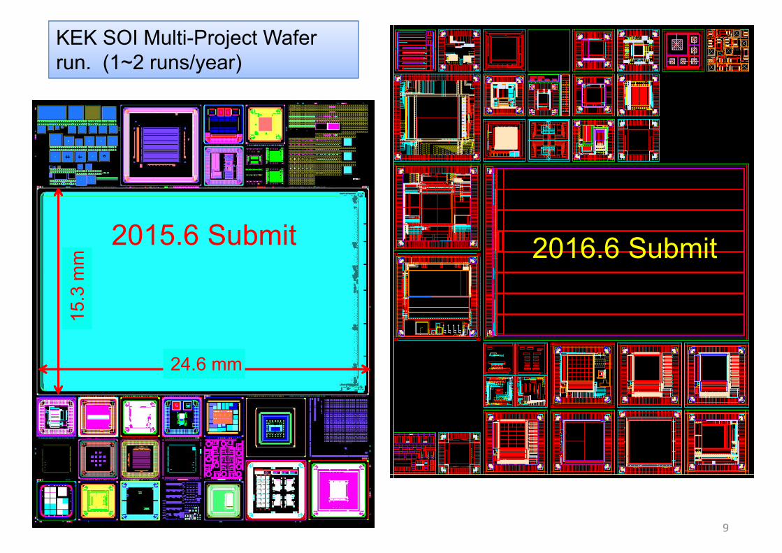
2015.6 Submit
24.6 mm
15.3
mm
KEK SOI Multi-Project Wafer run. (1~2 runs/year)
2016.6 Submit
9

II. Recent Progress
*Double SOI Wafer & Process
*Higher Dose LDD
*Layout Shrinking with NMOS‐PMOS merge
10

Transistor
SensorContact
Middle SiContact
Metal 5
Middle Si
Metal 1
Cross section of the Double SOI Pixel
11

Specification of Double SOI waferSpecification of Double SOI wafer
Layer Present Lot Next Lot
SOI1 p‐type 88 nm, < 10 •cm
p‐type 88 nm, < 10 •cm
BOX1 145 nm 145 nm
SOI2 n‐type 150 nm, < 10 •cm
n‐type 150 nm, 3‐5 •cm
BOX2 145 nm 145 nm
Substratep‐type
Low Oxygen Cz, 725um, > 1.0 k •cm
p‐typeFZ, 725um, > 5.0 k •cm
12

(by Lu Yunpeng (IHEP))(by Lu Yunpeng (IHEP))
Shield:Cross Talk between Circuit and Sensor is reduced to 1/20.
Single SOI
Double SOI
Effect of Double SOICross Talk from Clock line
13

Coupling:Gain of Charge Amp increases ~3 times by cutting parasitic C.
Effect of Double SOI
Single SOI
5fF
Double SOI
5fF
Gain49.2uV/e-
Gain15.3uV/e-
Am241
14

NMOS
Gamma-ray Irradiation Test(Id-Vg Characteristics v.s. SOI2 Potential)
By setting Middle Si potential (Vsoi2) to -5V, Id-Vg curve returned nearly to pre-irradiation value at 100 kGy(Si) (10 Mrad).
VSOI2=0V VSOI2=-2V VSOI2=-5V
Vg[V] Vg[V] Vg[V]
I d[A]
I d[A]
I d[A]
0 kGy 0 kGy 0 kGy
I/O normal VthSource‐Tie Tr.L/W =0.35um/5um
100 kGy 100 kGy
(by U. of Tsukuba)(by U. of Tsukuba)15

*Double SOI Wafer & Process
*Higher Dose LDD
*Layout Shrinking with NMOS‐PMOS merge
16

PMOSVariation of Id-Vg Characteristics and Effect of SOI2 Potential
VSOI2=0V VSOI2=-2V VSOI2=-5V
Vg[V]
I d[A]
I d[A]
I d[A]
0 kGy 0 kGy 0 kGy
I/O Normal VtSource‐Tie L/W =0.35um/5um
100kGy 100kGy
Vds=‐0.1V
Line
arId
112kGy
‐80%Threshold voltage shift is not so large in PMOS, but Drain Current decreases much .
17

18
Radiation Effect to
NMOS & PMOS
In PMOS, effective Gate Length become longer and Channel Resistance is increased with radiation. Radiation Induced Gate LEngth Modulation (RIGLEM).

• Major cause of the drain current degradation by radiation is Vth increase at gate edge due to positive charge generation in spacer.
• Charge in spacer control the Vth of the parasitic transistor.• To reduce this effect, lightly doped drain (LDD) dose should be
increased.• Present process has rather low dose in LDD region to aiming lower
power.
Gate
BOXP+ P+P‐ P‐
LDD(Lightly Doped Drain)
(by I. Kurachi)
Parasitic transistorParasitic transistor
Dose Increase in Lightly Doped Drain (LDD) Region
++ ++
19

Id‐Vg Characteristics in Triode Region
Vds=‐0.1V
Present Process
Line
arId
Ref.) I. Kurachi, et al. "Analysis of Effective Gate Length Modulation by X‐Ray Irradiation for Fully Depleted SOI p‐MOSFETs, IEEE Trans. on Elec. Dev. Vol. 62, Aug. 2015, pp. 2371‐2376.
112kGy
0kGy
With increasing Implantation dose of PLDD region 6 times higher than present value, the degradation is reduced from 80% to 20% at 112 kGy(Si).
LDD Dose x 6
112kGy
Vds=‐0.1V
0kGy
20

*Double SOI Wafer & Process
*Higher Dose LDD
*Layout Shrinking with NMOS‐PMOS merge
21

Lapis Semi.(*) 0.2 m FD-SOI Pixel Process
Process 0.2m Low-Leakage Fully-Depleted SOI CMOS 1 Poly, 5 Metal layers.MIM Capacitor (1.5 fF/um2), DMOSCore (I/O) Voltage = 1.8 (3.3) V
SOI wafer
Diameter: 200 mm, 720 m thickTop Si : Cz, ~18 -cm, p-type, ~40 nm thick Buried Oxide: 200 nm thickHandle wafer: Cz (n) ~700 -cm,
FZ(n) > 2k -cm, FZ(p) ~25 k -cm etc.
Backside process
Mechanical Grind, Chemical Etching, Back side Implant, Laser Annealing and Al plating
(*) Former OKI Semiconductor Co. Ltd. 22

Layout Shrink (Active Merge)PMOS NMOS
PMOS NMOS
N-Well P-Well
Bulk CMOS
SOI
ShareContacts
SalicideConnectionSalicideConnection
In the SOI process, it is possible to merge NMOS & PMOS Active region and share contacts.
23

Single Port SRAM Bit Cell
Cell Size : 3.94m X 3.06m = 12.06m2
WL
BL BLB
VDD
VSS
PchNch Nch
Only 1 Active region
24

New D Flip‐Flop25% of Previous Cell
25

Charge Amp+
Shaper+
Discriminator+
Q Share Handling+
19bit Counter+
7bit register
(in 2,340 um2)
Hexagonal Counting-type Pixel (submitted in June)
Smallest Counting-type Pixel of this kind.(much smaller than designed in 0.13um process)
52um
45um
26

III. Examples of SOI Detectors
14.144mm
8.70
4mm
Needle
Acrylic Resin
Stent Wire
(INTPIX4)
27

(by R. Nishimura, K. Hirano (KEK)
• Sensor:INTPIX4 FZn, Backside Illumination• HV:200V、Integration Time:1ms、ScanTime:320ns/pix, 1000frame/event• KEK PF, X‐ray Energy:9.5keV• Took images for 0~180°at every 1 degree.
Dried Sardine
INTPIX4Pixel Size : 17 um x 17 umNo. of Pixel : 512 x 832 (= 425,984)Chip Size : 10.3 mm x 15.5 mm
Integration type detector & 3D CT
28

3mm
INTPIX4: Computed Tomography with Syncrotron X‐ray
(by R. Nishimura, K. Hirano (KEK) 29

60 mm
SOI Photon-Imaging Array Sensor (SOPHIAS)for X-ray Free Electron Laser (XFEL) SACLA
Utilization of SOPHIAS has been started for various experiments in SACLA@RIKEN.• Dynamics of Atomic Structure• Direct Observation of Chemical Reactions• etc.
Dual Sensor Camera
X-ray Tube Cu 22kV 400uA5000 frames accumulated (total exposure: 500 s)Sensor-detector:2m
30

Pixel
Mask Layout
Exposed Layout
Blind
Blind
Stitching Exposure for Large Sensor
31

SOPHIAS detector: Fluctuation of speckle pattern
Wave length: 0.155 nmCamera length: 7.7 mBeam E=8keV φ 30umDetector:SOPHIAS (30μm2 / pixel)
Frame rate:30 Hz (readout 8ms)
Sample:200 nm Si particle in PPG
0.008 nm‐1
3mm
Courtesy of Prof. Masunaga and Dr. Kudo. 32

8 sets
each column line
anal
og
part
digi
tal pa
rt
XRPIX5: Event Driven X-ray Astronomy Detector
Signal
Trigger
33

XRPIX5: Event Driven X-ray Astronomy Detector
XRPIX5
608 x 384 pixel array1 Pixel : 36 µm sq.
24.6 mm
15.3 mm
PGA
DECODER & TRIGGER PROCESSOR
21.9 mm
13.8 mm
13.9 keV
17.7 keV
20.8 keV
26.3 keV59.5 keV
4.1%580 eV(FWHM)
Pulse Height (ADU)
241Am Spectrum
Coun
ts
Readout Noise : 48 e- (rms)Temp : -60 ºCVBB : 100 V35 e- (rms) of XRPIX3b.
- Chip size : 24.6 mm x 15.3 mm- Pixel size : 36 µm sq.- # of pixel : 608 x 384 (= ~233k) - Thickness of sensor layer : 310 µm (CZ wafer)
500 µm (FZ wafer)
34

R&D for ILC Vertex Detector
SOFIST: SOI sensor for Fine measurement of Space and Time
Analog Memories & Time Stamp Memories
35

SOFIST Test Chip (Ver.2)
25um x 25um
Submitted last June
36
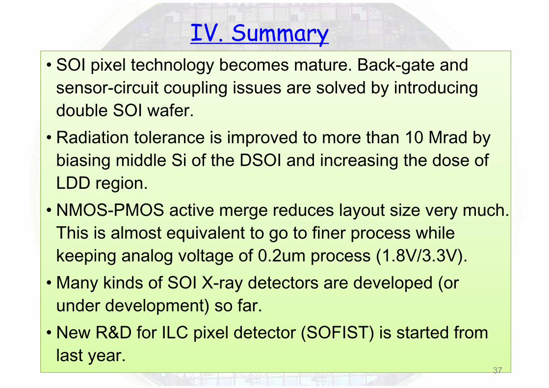
IV. Summary• SOI pixel technology becomes mature. Back-gate and
sensor-circuit coupling issues are solved by introducing double SOI wafer.
• Radiation tolerance is improved to more than 10 Mrad by biasing middle Si of the DSOI and increasing the dose of LDD region.
• NMOS-PMOS active merge reduces layout size very much. This is almost equivalent to go to finer process while keeping analog voltage of 0.2um process (1.8V/3.3V).
• Many kinds of SOI X-ray detectors are developed (or under development) so far.
• New R&D for ILC pixel detector (SOFIST) is started from last year.
37