unit-istudentsfocus.com/notes/anna_university/eee/5sem/ee6502 - mpmc...8085 microprocessor...
TRANSCRIPT
1
1 2
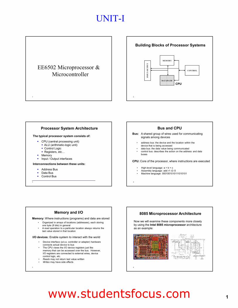
Building Blocks of Processor Systems
MEMORY
DATAPATH
CONTROL
INPUT-OUTPUT
CPU
3
Processor System Architecture
The typical processor system consists of:
! CPU (central processing unit)! ALU (arithmetic-logic unit)! Control Logic! Registers, etc…
! Memory! Input / Output interfaces
Interconnections between these units:
! Address Bus! Data Bus! Control Bus
4
Bus and CPUBus: A shared group of wires used for communicating
signals among devices
• address bus: the device and the location within the device that is being accessed
• data bus: the data value being communicated• control bus: describes the action on the address and data
buses
CPU: Core of the processor, where instructions are executed
• High-level language: a = b + c• Assembly language: add r1 r2 r3• Machine language: 0001001010111010101
5
Memory and I/OMemory: Where instructions (programs) and data are stored
• Organized in arrays of locations (addresses), each storing one byte (8 bits) in general
• A read operation to a particular location always returns the last value stored in that location
I/O devices: Enable system to interact with the world• Device interface (a.k.a. controller or adapter) hardware
connects actual device to bus• The CPU views the I/O device registers just like
memory that can be accessed over the bus. However, I/O registers are connected to external wires, device control logic, etc.
• Reads may not return last value written• Writes may have side effects
6
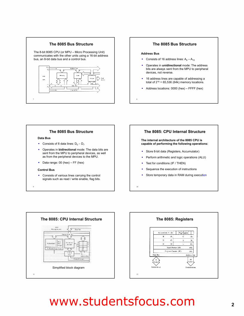
8085 Microprocessor Architecture
Now we will examine these components more closely by using the Intel 8085 microprocessor architecture as an example:
UNIT-I
EE6502 Microprocessor & Microcontroller
www.studentsfocus.com
2
7
The 8085 Bus Structure
The 8-bit 8085 CPU (or MPU – Micro Processing Unit) communicates with the other units using a 16-bit address bus, an 8-bit data bus and a control bus.
8
The 8085 Bus Structure
Address Bus
! Consists of 16 address lines: A0 – A15
! Operates in unidirectional mode: The address bits are always sent from the MPU to peripheral devices, not reverse.
! 16 address lines are capable of addressing a total of 216 = 65,536 (64k) memory locations.
! Address locations: 0000 (hex) – FFFF (hex)
9
The 8085 Bus StructureData Bus
! Consists of 8 data lines: D0 – D7
! Operates in bidirectional mode: The data bits are sent from the MPU to peripheral devices, as well as from the peripheral devices to the MPU.
! Data range: 00 (hex) – FF (hex)
Control Bus
! Consists of various lines carrying the control signals such as read / write enable, flag bits.
10
The 8085: CPU Internal Structure
The internal architecture of the 8085 CPU is capable of performing the following operations:
! Store 8-bit data (Registers, Accumulator)
! Perform arithmetic and logic operations (ALU)
! Test for conditions (IF / THEN)
! Sequence the execution of instructions
! Store temporary data in RAM during execution
11
The 8085: CPU Internal Structure
Simplified block diagram
12
The 8085: Registers
www.studentsfocus.com
3
13
The 8085: CPU Internal Structure
Registers
! Six general purpose 8-bit registers: B, C, D, E, H, L
! They can also be combined as register pairs to perform 16-bit operations: BC, DE, HL
! Registers are programmable (data load, move, etc.)
Accumulator
! Single 8-bit register that is part of the ALU !
! Used for arithmetic / logic operations – the result is always stored in the accumulator.
14
The 8085: CPU Internal Structure
Flag Bits
! Indicate the result of condition tests.
! Carry, Zero, Sign, Parity, etc.
! Conditional operations (IF / THEN) are executed based on the condition of these flag bits.
Program Counter (PC)
! Contains the memory address (16 bits) of the instruction that will be executed in the next step.
Stack Pointer (SP)
15
Example: Memory Read Operation
16
Example: Instruction Fetch Operation
! All instructions (program steps) are stored in memory.
! To run a program, the individual instructions must be read from the memory in sequence, and executed.
! Program counter puts the 16-bit memory address of the instruction on the address bus
! Control unit sends the Memory Read Enable signal to access the memory
! The 8-bit instruction stored in memory is placed on the data bus and transferred to the instruction decoder
! Instruction is decoded and executed
17
Example: Instruction Fetch Operation
18
Example: Instruction Fetch Operation
www.studentsfocus.com
4
19
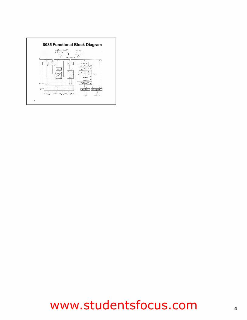
8085 Functional Block Diagram
www.studentsfocus.com
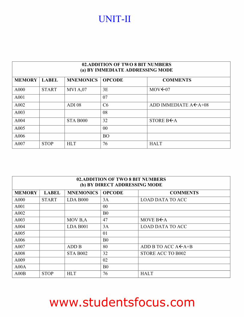
02.ADDITION OF TWO 8 BIT NUMBERS (b) BY DIRECT ADDRESSING MODE
MEMORY LABEL MNEMONICS OPCODE COMMENTS A000 START LDA B000 3A LOAD DATA TO ACC A001 00 A002 B0 A003 MOV B,A 47 MOVE B!A A004 LDA B001 3A LOAD DATA TO ACC A005 01 A006 B0 A007 ADD B 80 ADD B TO ACC A!A+B A008 STA B002 32 STORE ACC TO B002 A009 02 A00A B0 A00B STOP HLT 76 HALT
02.ADDITION OF TWO 8 BIT NUMBERS (a) BY IMMEDIATE ADDRESSING MODE
MEMORY LABEL MNEMONICS OPCODE COMMENTS
A000 START MVI A,07 3E MOV!07 A001 07 A002 ADI 08 C6 ADD IMMEDIATE A!A+08 A003 08
A004 STA B000 32 STORE B!A A005 00 A006 BO A007 STOP HLT 76 HALT
UNIT-II
www.studentsfocus.com
02.ADDITION OF TWO 8 BIT NUMBERS (C) BY INDIRECT ADDRESSING MODE
MEMORY LABEL MNEMONICS OPCODE COMMENTS
A000 START LXI H,B000 21 LOAD DATA IN HL PAIR
A001 00
A002 B0
A003 MOV A,M 7E MOVE A!M
A004 INX H 23 INCREMENT H
A005 ADD M 86 ADD A!A+M
A006 INX H 23 INCREMENT H
A007 MOV M,A 77 MOVE M!A
A008 STOP HLT 76 HALT
02.ADDITION OF TWO 8 BIT NUMBERS (d) ADDITION WITH CARRY
MEMORY LABEL MNEMONICS OPCODE COMMENTS
A000 START MVI C,00 0E,00 (C)"00
A002 LDA 8050 3A,50,80 ACC"(8050)
A005 MOV B,A 47 (B)"A
A006 LDA 8051 3A,51,80 ACC"(8051)
A009 ADD B 80 A!(A)+(B)
A00A STA 8052 32,53,80 (8052)!(A)
A00D MVI A,00 3E,00 (A)!00
A00F STA 8053 32,53,80 (8053)!(A)
A012 JNC A01A D2,10,A0 JUMP TO AO1A IF ZERO CARRY
A015 INR C 0C INCREMENT C
A016 MOV A,C 79 (C)"(A)
A017 JNC STA 8053 32,53,80 (A)"(8053)
A01A STOP HLT 76 HALT
www.studentsfocus.com
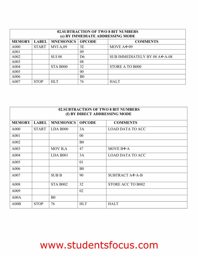
02.SUBTRACTION OF TWO 8 BIT NUMBERS (e) BY IMMEDIATE ADDRESSING MODE
MEMORY LABEL MNEMONICS OPCODE COMMENTS A000 START MVI A,09 3E MOVE A!09 A001 09 A002 SUI 08 D6 SUB IMMEDIATELY BY 08 A!A-08 A003 08 A004 STA B000 32 STORE A TO B000 A005 00 A006 B0 A007 STOP HLT 76 HALT
02.SUBTRACTION OF TWO 8 BIT NUMBERS (f) BY DIRECT ADDRESSING MODE
MEMORY LABEL MNEMONICS OPCODE COMMENTS A000 START LDA B000 3A LOAD DATA TO ACC
A001 00
A002 B0
A003 MOV B,A 47 MOVE B!A
A004 LDA B001 3A LOAD DATA TO ACC
A005 01
A006 B0
A007 SUB B 90 SUBTRACT A!A-B
A008 STA B002 32 STORE ACC TO B002
A009 02
A00A B0
A00B STOP 76 HLT HALT
www.studentsfocus.com
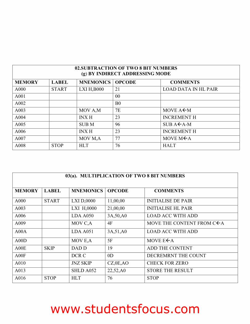
02.SUBTRACTION OF TWO 8 BIT NUMBERS (g) BY INDIRECT ADDRESSING MODE
MEMORY LABEL MNEMONICS OPCODE COMMENTS A000 START LXI H,B000 21 LOAD DATA IN HL PAIR A001 00 A002 B0 A003 MOV A,M 7E MOVE A!M A004 INX H 23 INCREMENT H A005 SUB M 96 SUB A!A-M A006 INX H 23 INCREMENT H A007 MOV M,A 77 MOVE M!A A008 STOP HLT 76 HALT
03(a). MULTIPLICATION OF TWO 8 BIT NUMBERS
MEMORY LABEL MNEMONICS OPCODE COMMENTS
A000 START LXI D,0000 11,00,00 INITIALISE DE PAIR A003 LXI H,0000 21,00,00 INITIALISE HL PAIR A006 LDA A050 3A,50,A0 LOAD ACC WITH ADD A009 MOV C,A 4F MOVE THE CONTENT FROM C!A
A00A LDA A051 3A,51,A0 LOAD ACC WITH ADD
A00D MOV E,A 5F MOVE E!A A00E SKIP DAD D 19 ADD THE CONTENT A00F DCR C 0D DECREMRNT THE COUNT A010 JNZ SKIP CZ,0E,AO CHECK FOR ZERO A013 SHLD A052 22,52,A0 STORE THE RESULT A016 STOP HLT 76 STOP
www.studentsfocus.com
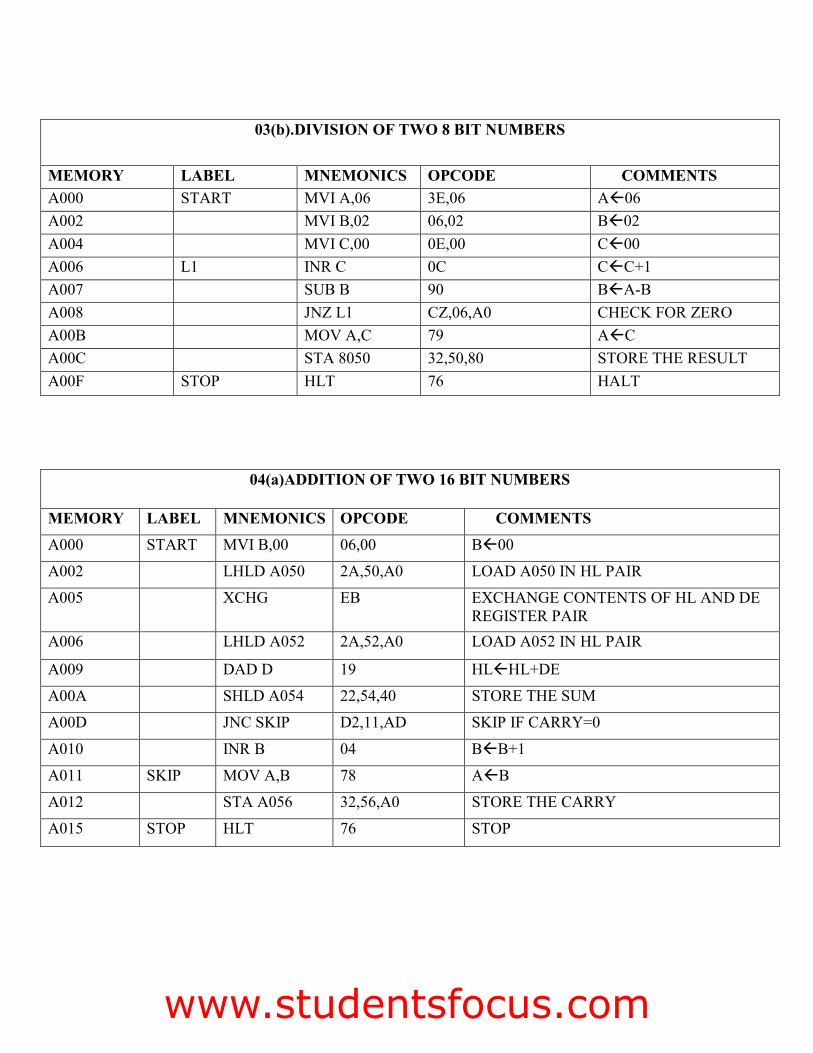
03(b).DIVISION OF TWO 8 BIT NUMBERS
MEMORY LABEL MNEMONICS OPCODE COMMENTS A000 START MVI A,06 3E,06 A!06 A002 MVI B,02 06,02 B!02 A004 MVI C,00 0E,00 C!00 A006 L1 INR C 0C C!C+1 A007 SUB B 90 B!A-B A008 JNZ L1 CZ,06,A0 CHECK FOR ZERO A00B MOV A,C 79 A!C A00C STA 8050 32,50,80 STORE THE RESULT A00F STOP HLT 76 HALT
04(a)ADDITION OF TWO 16 BIT NUMBERS
MEMORY LABEL MNEMONICS OPCODE COMMENTS A000 START MVI B,00 06,00 B!00
A002 LHLD A050 2A,50,A0 LOAD A050 IN HL PAIR
A005 XCHG EB EXCHANGE CONTENTS OF HL AND DE REGISTER PAIR
A006 LHLD A052 2A,52,A0 LOAD A052 IN HL PAIR
A009 DAD D 19 HL!HL+DE
A00A SHLD A054 22,54,40 STORE THE SUM
A00D JNC SKIP D2,11,AD SKIP IF CARRY=0
A010 INR B 04 B!B+1
A011 SKIP MOV A,B 78 A!B
A012 STA A056 32,56,A0 STORE THE CARRY
A015 STOP HLT 76 STOP
www.studentsfocus.com
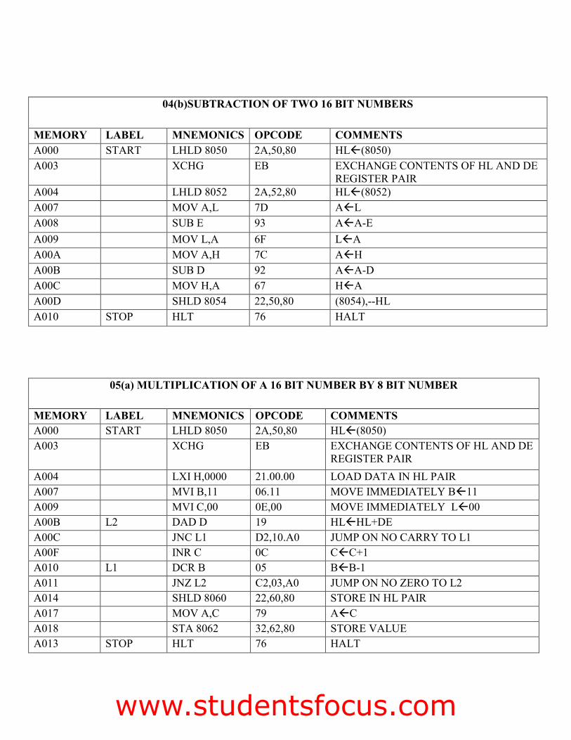
04(b)SUBTRACTION OF TWO 16 BIT NUMBERS
MEMORY LABEL MNEMONICS OPCODE COMMENTS A000 START LHLD 8050 2A,50,80 HL!(8050) A003 XCHG EB EXCHANGE CONTENTS OF HL AND DE
REGISTER PAIR A004 LHLD 8052 2A,52,80 HL!(8052) A007 MOV A,L 7D A!L A008 SUB E 93 A!A-E A009 MOV L,A 6F L!A A00A MOV A,H 7C A!H A00B SUB D 92 A!A-D A00C MOV H,A 67 H!A A00D SHLD 8054 22,50,80 (8054),--HL A010 STOP HLT 76 HALT
05(a) MULTIPLICATION OF A 16 BIT NUMBER BY 8 BIT NUMBER
MEMORY LABEL MNEMONICS OPCODE COMMENTS A000 START LHLD 8050 2A,50,80 HL!(8050) A003 XCHG EB EXCHANGE CONTENTS OF HL AND DE
REGISTER PAIR A004 LXI H,0000 21.00.00 LOAD DATA IN HL PAIR A007 MVI B,11 06.11 MOVE IMMEDIATELY B!11 A009 MVI C,00 0E,00 MOVE IMMEDIATELY L!00 A00B L2 DAD D 19 HL!HL+DE A00C JNC L1 D2,10.A0 JUMP ON NO CARRY TO L1 A00F INR C 0C C!C+1 A010 L1 DCR B 05 B!B-1 A011 JNZ L2 C2,03,A0 JUMP ON NO ZERO TO L2 A014 SHLD 8060 22,60,80 STORE IN HL PAIR A017 MOV A,C 79 A!C A018 STA 8062 32,62,80 STORE VALUE A013 STOP HLT 76 HALT
www.studentsfocus.com
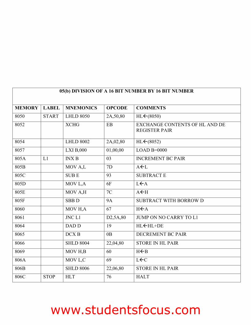
05(b) DIVISION OF A 16 BIT NUMBER BY 16 BIT NUMBER
MEMORY LABEL MNEMONICS OPCODE COMMENTS
8050 START LHLD 8050 2A,50,80 HL!(8050)
8052 XCHG EB EXCHANGE CONTENTS OF HL AND DE REGISTER PAIR
8054 LHLD 8002 2A,02,80 HL!(8052)
8057 LXI B,000 01,00,00 LOAD B=0000
805A L1 INX B 03 INCREMENT BC PAIR
805B MOV A,L 7D A!L
805C SUB E 93 SUBTRACT E
805D MOV L,A 6F L!A
805E MOV A,H 7C A!H
805F SBB D 9A SUBTRACT WITH BORROW D
8060 MOV H,A 67 H!A
8061 JNC L1 D2,5A,80 JUMP ON NO CARRY TO L1
8064 DAD D 19 HL!HL+DE
8065 DCX B 0B DECREMENT BC PAIR
8066 SHLD 8004 22,04,80 STORE IN HL PAIR
8069 MOV H,B 60 H!B
806A MOV L,C 69 L!C
806B SHLD 8006 22,06,80 STORE IN HL PAIR
806C STOP HLT 76 HALT
www.studentsfocus.com
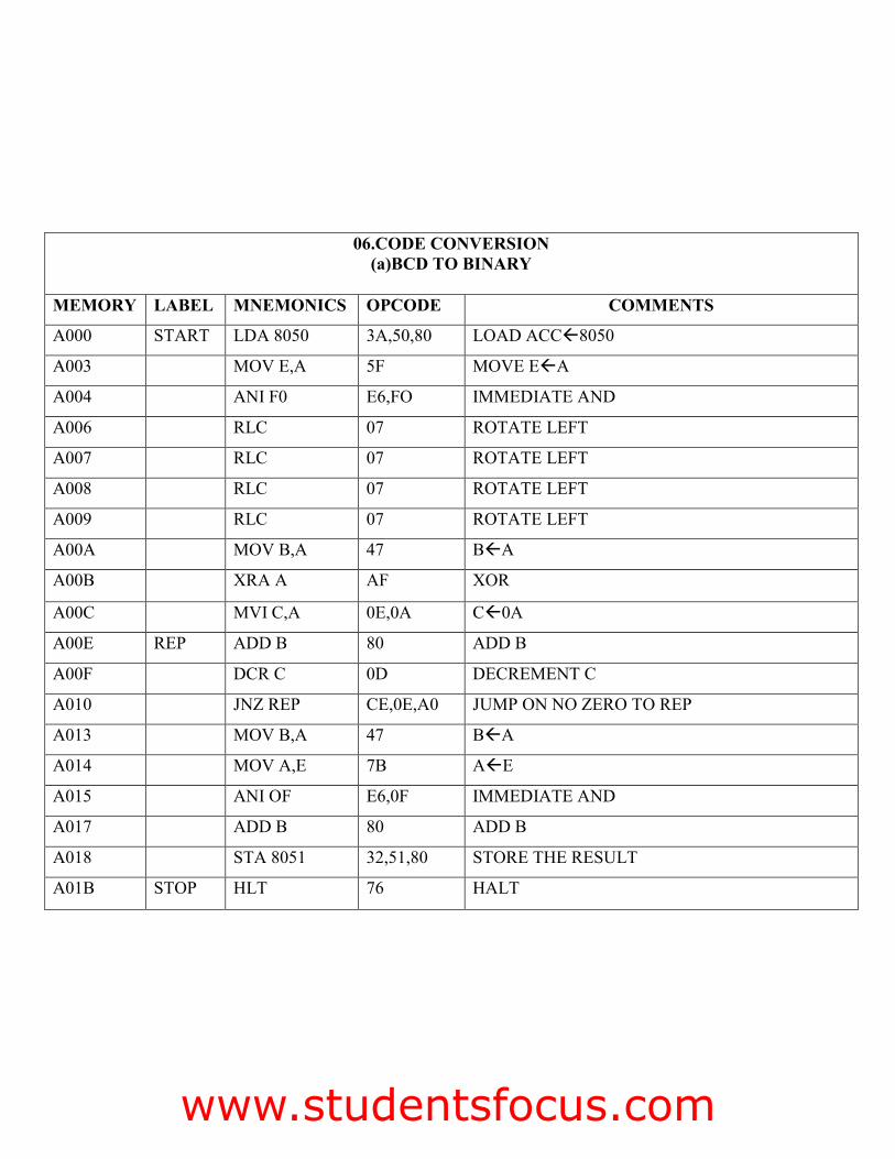
06.CODE CONVERSION (a)BCD TO BINARY
MEMORY LABEL MNEMONICS OPCODE COMMENTS
A000 START LDA 8050 3A,50,80 LOAD ACC!8050
A003 MOV E,A 5F MOVE E!A
A004 ANI F0 E6,FO IMMEDIATE AND
A006 RLC 07 ROTATE LEFT
A007 RLC 07 ROTATE LEFT
A008 RLC 07 ROTATE LEFT
A009 RLC 07 ROTATE LEFT
A00A MOV B,A 47 B!A
A00B XRA A AF XOR
A00C MVI C,A 0E,0A C!0A
A00E REP ADD B 80 ADD B
A00F DCR C 0D DECREMENT C
A010 JNZ REP CE,0E,A0 JUMP ON NO ZERO TO REP
A013 MOV B,A 47 B!A
A014 MOV A,E 7B A!E
A015 ANI OF E6,0F IMMEDIATE AND
A017 ADD B 80 ADD B
A018 STA 8051 32,51,80 STORE THE RESULT
A01B STOP HLT 76 HALT
www.studentsfocus.com
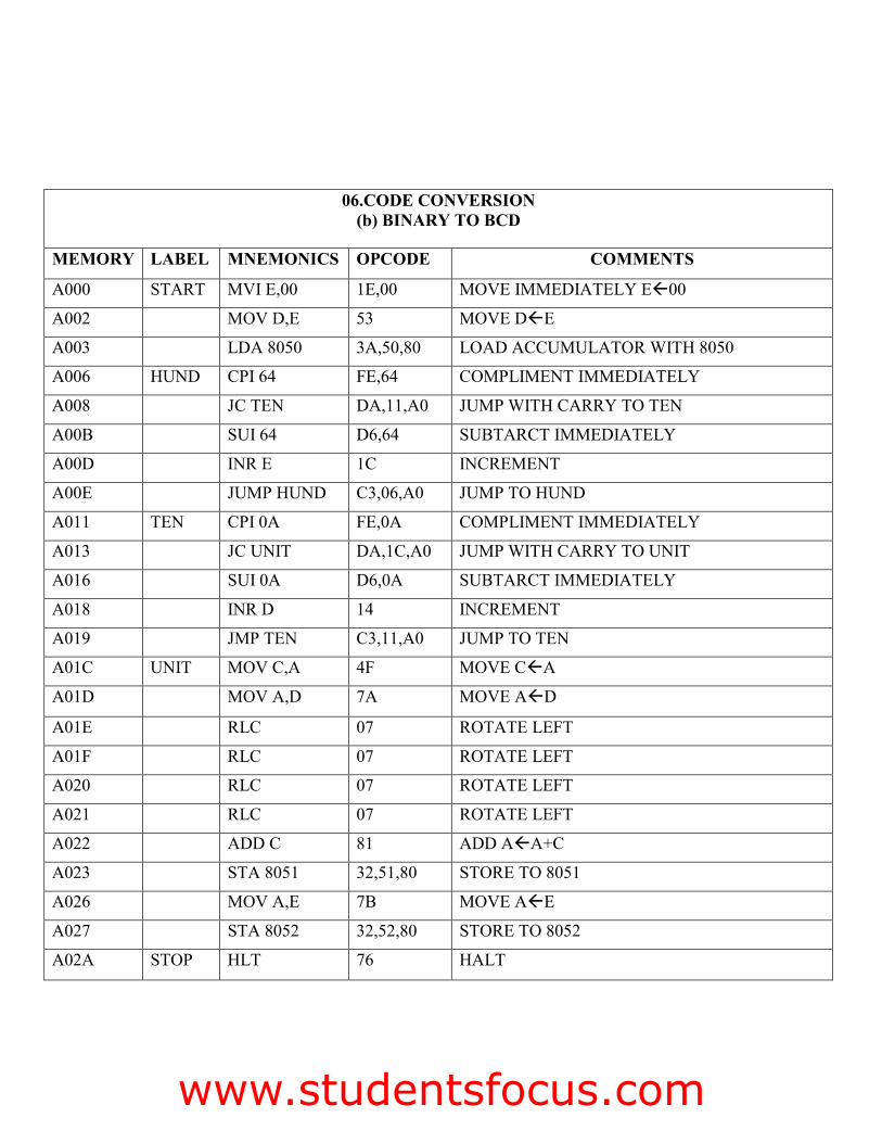
06.CODE CONVERSION (b) BINARY TO BCD
MEMORY LABEL MNEMONICS OPCODE COMMENTS
A000 START MVI E,00 1E,00 MOVE IMMEDIATELY E!00
A002 MOV D,E 53 MOVE D!E
A003 LDA 8050 3A,50,80 LOAD ACCUMULATOR WITH 8050
A006 HUND CPI 64 FE,64 COMPLIMENT IMMEDIATELY
A008 JC TEN DA,11,A0 JUMP WITH CARRY TO TEN
A00B SUI 64 D6,64 SUBTARCT IMMEDIATELY
A00D INR E 1C INCREMENT
A00E JUMP HUND C3,06,A0 JUMP TO HUND
A011 TEN CPI 0A FE,0A COMPLIMENT IMMEDIATELY
A013 JC UNIT DA,1C,A0 JUMP WITH CARRY TO UNIT
A016 SUI 0A D6,0A SUBTARCT IMMEDIATELY
A018 INR D 14 INCREMENT
A019 JMP TEN C3,11,A0 JUMP TO TEN
A01C UNIT MOV C,A 4F MOVE C!A
A01D MOV A,D 7A MOVE A!D
A01E RLC 07 ROTATE LEFT
A01F RLC 07 ROTATE LEFT
A020 RLC 07 ROTATE LEFT
A021 RLC 07 ROTATE LEFT
A022 ADD C 81 ADD A!A+C
A023 STA 8051 32,51,80 STORE TO 8051
A026 MOV A,E 7B MOVE A!E
A027 STA 8052 32,52,80 STORE TO 8052
A02A STOP HLT 76 HALT
www.studentsfocus.com
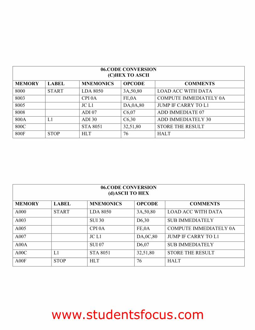
06.CODE CONVERSION (C)HEX TO ASCII
MEMORY LABEL MNEMONICS OPCODE COMMENTS 8000 START LDA 8050 3A,50,80 LOAD ACC WITH DATA 8003 CPI 0A FE,0A COMPUTE IMMEDIATELY 0A 8005 JC L1 DA,0A,80 JUMP IF CARRY TO L1 8008 ADI 07 C6,07 ADD IMMEDIATE 07 800A L1 ADI 30 C6,30 ADD IMMEDIATELY 30 800C STA 8051 32,51,80 STORE THE RESULT 800F STOP HLT 76 HALT
06.CODE CONVERSION (d)ASCII TO HEX
MEMORY LABEL MNEMONICS OPCODE COMMENTS A000 START LDA 8050 3A,50,80 LOAD ACC WITH DATA
A003 SUI 30 D6,30 SUB IMMEDIATELY A005 CPI 0A FE,0A COMPUTE IMMEDIATELY 0A A007 JC L1 DA,0C,80 JUMP IF CARRY TO L1 A00A SUI 07 D6,07 SUB IMMEDIATELY A00C L1 STA 8051 32,51,80 STORE THE RESULT A00F STOP HLT 76 HALT
www.studentsfocus.com
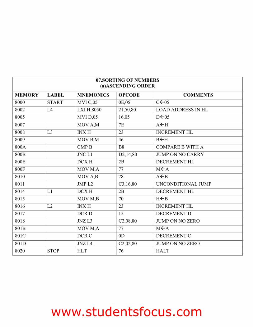
07.SORTING OF NUMBERS (a)ASCENDING ORDER
MEMORY LABEL MNEMONICS OPCODE COMMENTS 8000 START MVI C,05 0E,05 C!05 8002 L4 LXI H,8050 21,50,80 LOAD ADDRESS IN HL 8005 MVI D,05 16,05 D!05 8007 MOV A,M 7E A!H 8008 L3 INX H 23 INCREMENT HL 8009 MOV B,M 46 B!H 800A CMP B B8 COMPARE B WITH A 800B JNC L1 D2,14,80 JUMP ON NO CARRY 800E DCX H 2B DECREMENT HL 800F MOV M,A 77 M!A 8010 MOV A,B 78 A!B 8011 JMP L2 C3,16,80 UNCONDITIONAL JUMP 8014 L1 DCX H 2B DECREMENT HL 8015 MOV M,B 70 H!B 8016 L2 INX H 23 INCREMENT HL 8017 DCR D 15 DECREMENT D 8018 JNZ L3 C2,08,80 JUMP ON NO ZERO 801B MOV M,A 77 M!A 801C DCR C 0D DECREMENT C 801D JNZ L4 C2,02,80 JUMP ON NO ZERO 8020 STOP HLT 76 HALT
www.studentsfocus.com
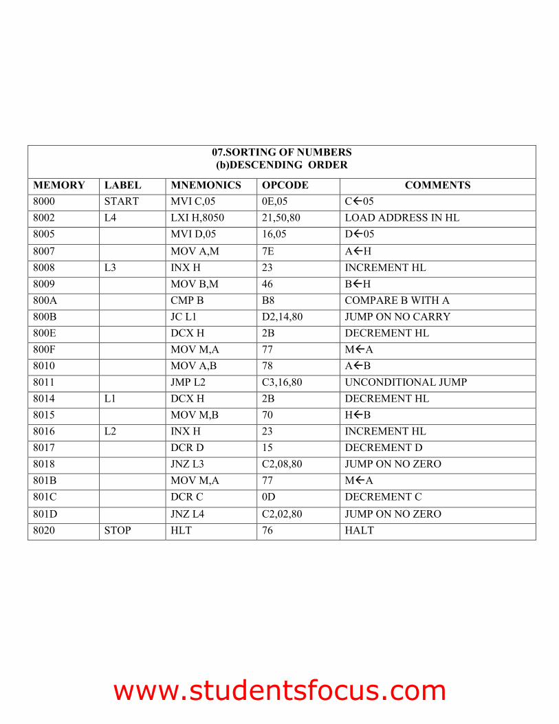
07.SORTING OF NUMBERS (b)DESCENDING ORDER
MEMORY LABEL MNEMONICS OPCODE COMMENTS 8000 START MVI C,05 0E,05 C!05 8002 L4 LXI H,8050 21,50,80 LOAD ADDRESS IN HL 8005 MVI D,05 16,05 D!05 8007 MOV A,M 7E A!H 8008 L3 INX H 23 INCREMENT HL 8009 MOV B,M 46 B!H 800A CMP B B8 COMPARE B WITH A 800B JC L1 D2,14,80 JUMP ON NO CARRY 800E DCX H 2B DECREMENT HL 800F MOV M,A 77 M!A 8010 MOV A,B 78 A!B 8011 JMP L2 C3,16,80 UNCONDITIONAL JUMP 8014 L1 DCX H 2B DECREMENT HL 8015 MOV M,B 70 H!B 8016 L2 INX H 23 INCREMENT HL 8017 DCR D 15 DECREMENT D 8018 JNZ L3 C2,08,80 JUMP ON NO ZERO 801B MOV M,A 77 M!A 801C DCR C 0D DECREMENT C 801D JNZ L4 C2,02,80 JUMP ON NO ZERO 8020 STOP HLT 76 HALT
www.studentsfocus.com
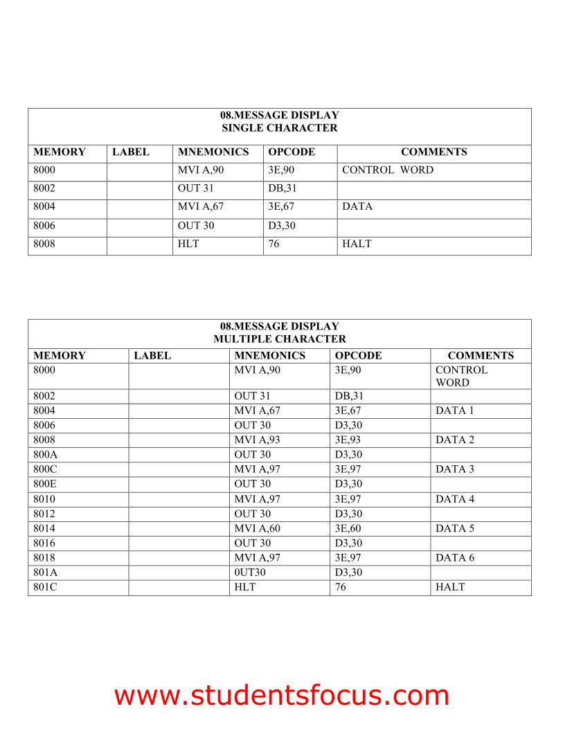
08.MESSAGE DISPLAY SINGLE CHARACTER
MEMORY LABEL MNEMONICS OPCODE COMMENTS 8000 MVI A,90 3E,90 CONTROL WORD
8002 OUT 31 DB,31
8004 MVI A,67 3E,67 DATA
8006 OUT 30 D3,30
8008 HLT 76 HALT
08.MESSAGE DISPLAY MULTIPLE CHARACTER
MEMORY LABEL MNEMONICS OPCODE COMMENTS 8000 MVI A,90 3E,90 CONTROL
WORD 8002 OUT 31 DB,31 8004 MVI A,67 3E,67 DATA 1 8006 OUT 30 D3,30 8008 MVI A,93 3E,93 DATA 2 800A OUT 30 D3,30 800C MVI A,97 3E,97 DATA 3 800E OUT 30 D3,30 8010 MVI A,97 3E,97 DATA 4 8012 OUT 30 D3,30 8014 MVI A,60 3E,60 DATA 5 8016 OUT 30 D3,30 8018 MVI A,97 3E,97 DATA 6 801A 0UT30 D3,30 801C HLT 76 HALT
www.studentsfocus.com
1
1
Contents
• Introduction• Block Diagram and Pin Description of the 8051• Instruction format and addressing modes • Interrupt structure • Timer• I/O ports • Serial communication
MICRO CONTROLLER 8051III UNIT
www.studentsfocus.com
2
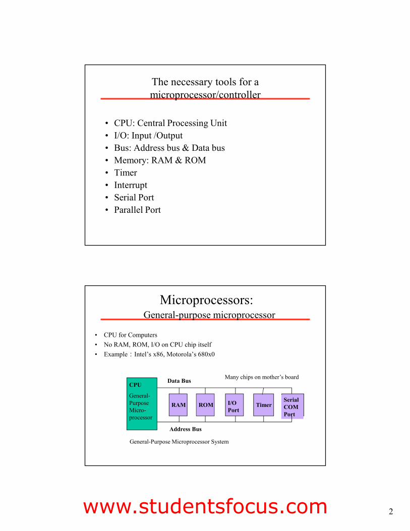
The necessary tools for a microprocessor/controller
• CPU: Central Processing Unit• I/O: Input /Output• Bus: Address bus & Data bus• Memory: RAM & ROM• Timer• Interrupt• Serial Port• Parallel Port
CPU
General-Purpose Micro-processor
RAM ROM I/O Port
TimerSerial COM Port
Data Bus
Address Bus
General-Purpose Microprocessor System
Microprocessors:
• CPU for Computers• No RAM, ROM, I/O on CPU chip itself• Example᧶Intel’s x86, Motorola’s 680x0
Many chips on mother’s board
General-purpose microprocessor
www.studentsfocus.com
3
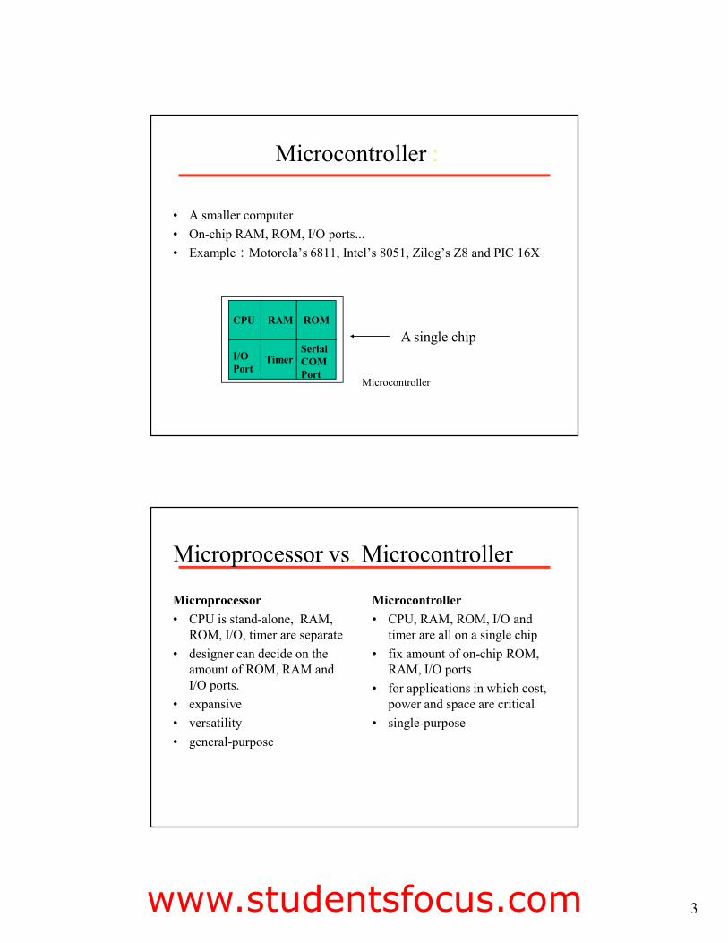
RAM ROM
I/O Port
TimerSerial COM Port
Microcontroller
CPU
• A smaller computer• On-chip RAM, ROM, I/O ports...• Example᧶Motorola’s 6811, Intel’s 8051, Zilog’s Z8 and PIC 16X
A single chip
Microcontroller :
Microprocessor• CPU is stand-alone, RAM,
ROM, I/O, timer are separate• designer can decide on the
amount of ROM, RAM and I/O ports.
• expansive• versatility • general-purpose
Microcontroller• CPU, RAM, ROM, I/O and
timer are all on a single chip• fix amount of on-chip ROM,
RAM, I/O ports• for applications in which cost,
power and space are critical• single-purpose
Microprocessor vs. Microcontroller
www.studentsfocus.com
4
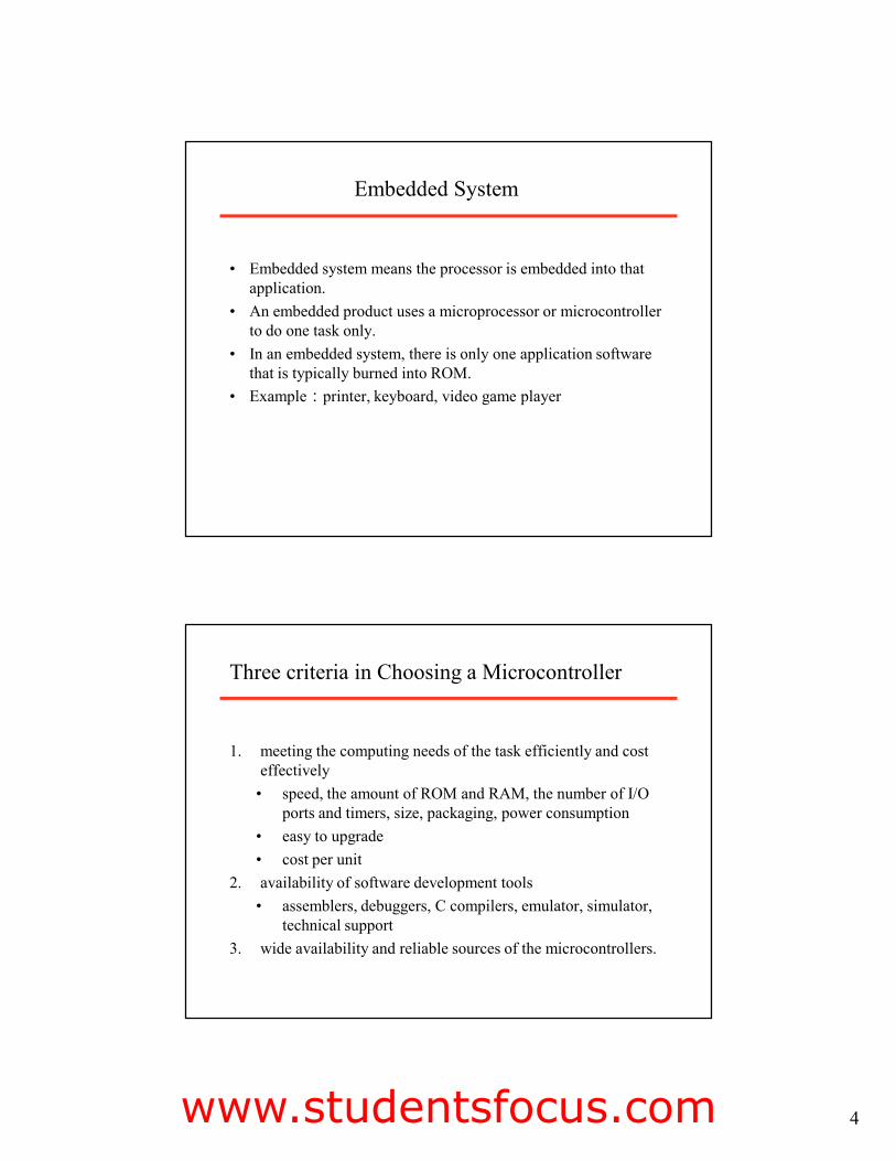
• Embedded system means the processor is embedded into that application.
• An embedded product uses a microprocessor or microcontroller to do one task only.
• In an embedded system, there is only one application software that is typically burned into ROM.
• Example᧶printer, keyboard, video game player
Embedded System
1. meeting the computing needs of the task efficiently and cost effectively
• speed, the amount of ROM and RAM, the number of I/O ports and timers, size, packaging, power consumption
• easy to upgrade• cost per unit
2. availability of software development tools• assemblers, debuggers, C compilers, emulator, simulator,
technical support3. wide availability and reliable sources of the microcontrollers.
Three criteria in Choosing a Microcontroller
www.studentsfocus.com
5
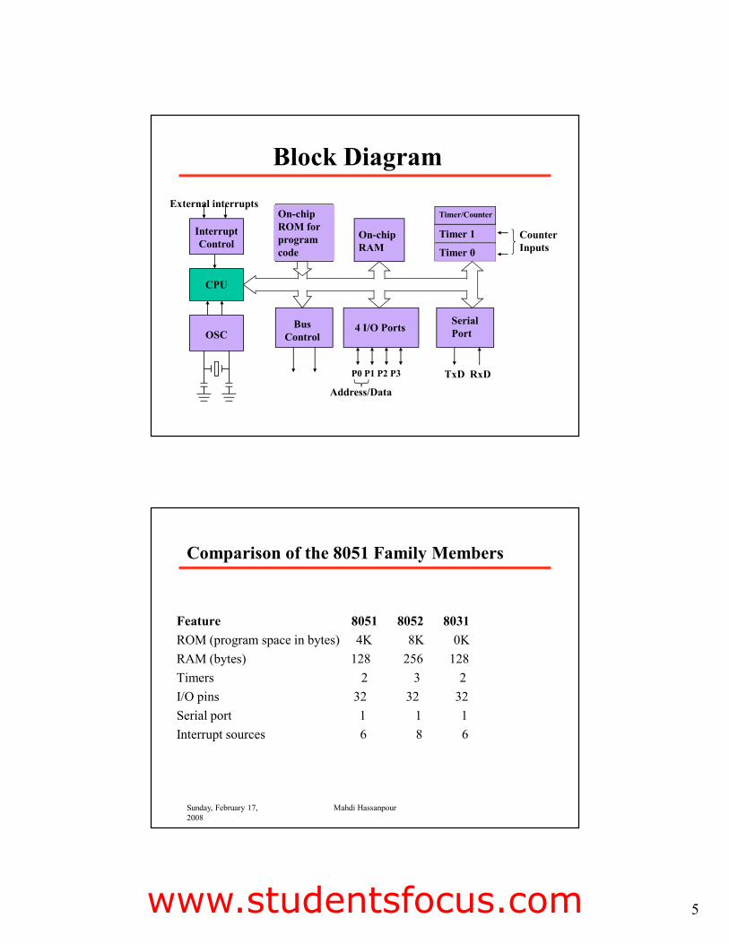
Block Diagram
CPU
On-chip RAM
On-chip ROM for program code
4 I/O Ports
Timer 0
Serial PortOSC
Interrupt Control
External interrupts
Timer 1
Timer/Counter
Bus Control
TxD RxDP0 P1 P2 P3
Address/Data
Counter Inputs
Sunday, February 17, 2008
Mahdi Hassanpour
Feature 8051 8052 8031ROM (program space in bytes) 4K 8K 0KRAM (bytes) 128 256 128Timers 2 3 2I/O pins 32 32 32 Serial port 1 1 1 Interrupt sources 6 8 6
Comparison of the 8051 Family Members
www.studentsfocus.com
6
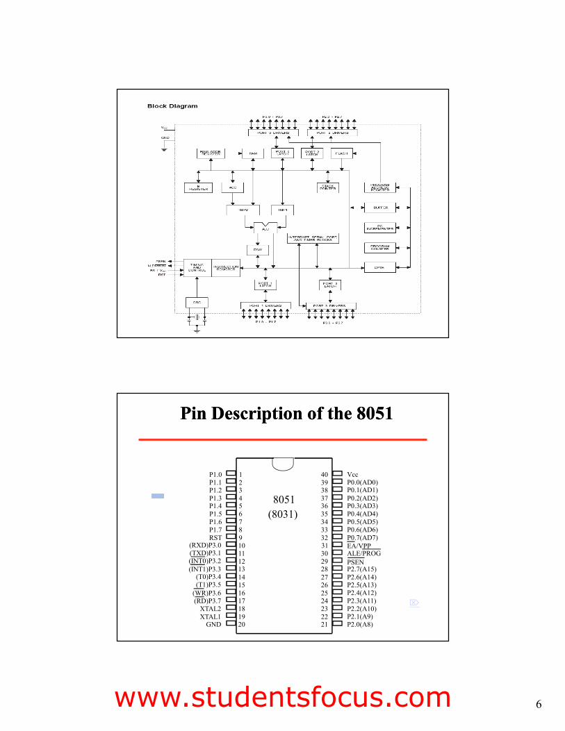
Pin Description of the 8051Pin Description of the 8051
1234567891011121314151617181920
4039383736353433323130292827262524232221
P1.0P1.1P1.2P1.3P1.4P1.5P1.6P1.7RST
(RXD)P3.0(TXD)P3.1
(T0)P3.4(T1)P3.5
XTAL2XTAL1
GND
(INT0)P3.2(INT1)P3.3
(RD)P3.7(WR)P3.6
VccP0.0(AD0)P0.1(AD1)P0.2(AD2)P0.3(AD3)P0.4(AD4)P0.5(AD5)P0.6(AD6)P0.7(AD7)EA/VPPALE/PROGPSENP2.7(A15)P2.6(A14)P2.5(A13)P2.4(A12)P2.3(A11)P2.2(A10)P2.1(A9)P2.0(A8)
8051(8031)
www.studentsfocus.com
7
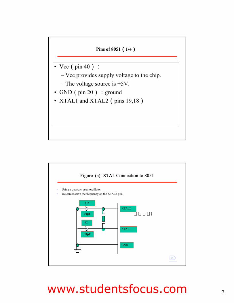
Pins of 8051᧤᧤᧤᧤1/4᧥᧥᧥᧥
• Vcc᧤pin 40᧥᧶– Vcc provides supply voltage to the chip. – The voltage source is +5V.
• GND᧤pin 20᧥᧶ground• XTAL1 and XTAL2᧤pins 19,18᧥
Figure (a). XTAL Connection to 8051Figure (a). XTAL Connection to 8051
C2
30pF
C1
30pF
XTAL2
XTAL1
GND
" Using a quartz crystal oscillator" We can observe the frequency on the XTAL2 pin.
www.studentsfocus.com
8
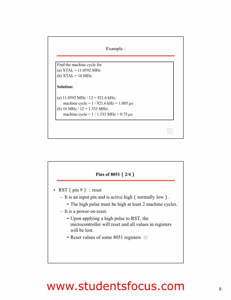
Example :
Find the machine cycle for(a) XTAL = 11.0592 MHz (b) XTAL = 16 MHz.
Solution:
(a) 11.0592 MHz / 12 = 921.6 kHz;machine cycle = 1 / 921.6 kHz = 1.085 µs
(b) 16 MHz / 12 = 1.333 MHz;machine cycle = 1 / 1.333 MHz = 0.75 µs
Pins of 8051᧤᧤᧤᧤2/4᧥᧥᧥᧥
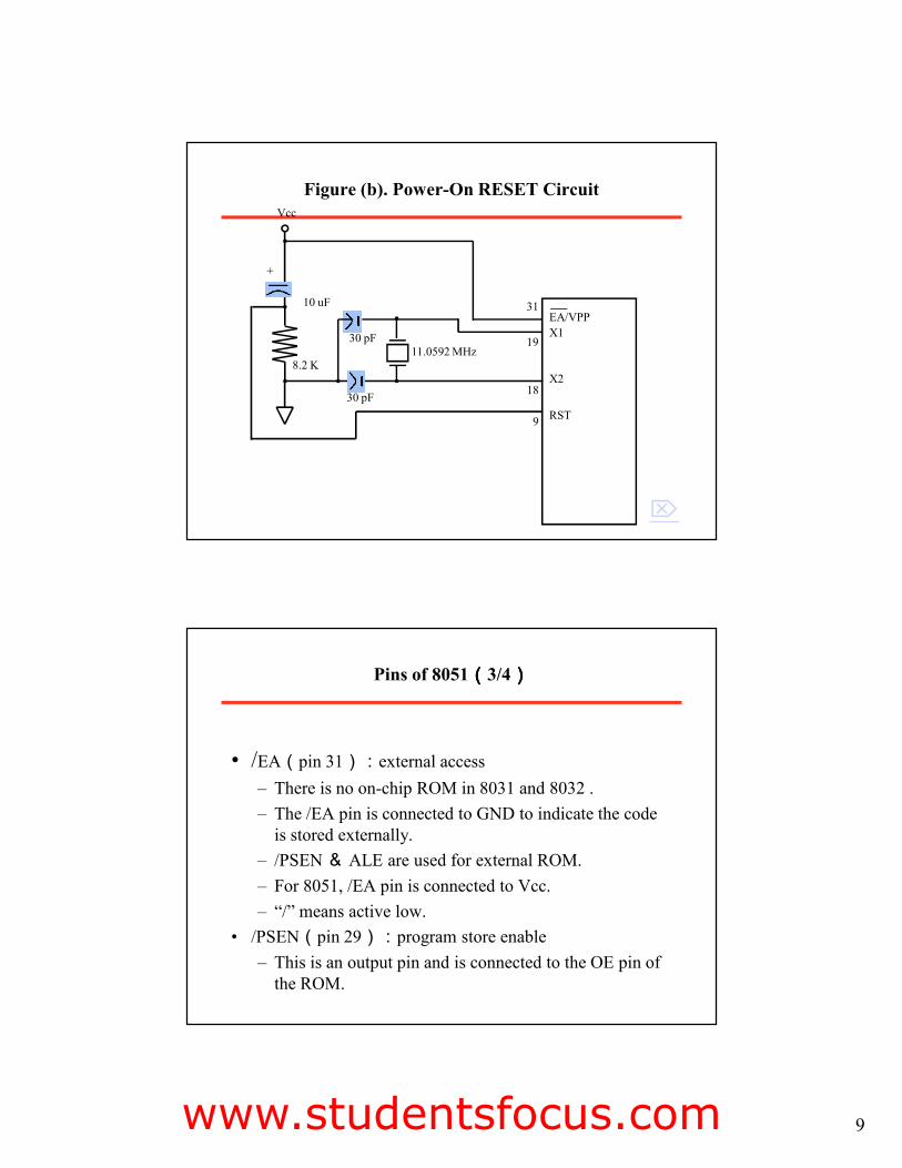
• RST᧤pin 9᧥᧶reset– It is an input pin and is active high᧤normally low᧥.
• The high pulse must be high at least 2 machine cycles.– It is a power-on reset.
• Upon applying a high pulse to RST, the microcontroller will reset and all values in registers will be lost.
• Reset values of some 8051 registers #
www.studentsfocus.com
9
Figure (b). Power-On RESET Circuit
30 pF
30 pF
8.2 K
10 uF
+
Vcc
11.0592 MHz
EA/VPPX1
X2
RST
31
19
18
9
Pins of 8051᧤᧤᧤᧤3/4᧥᧥᧥᧥
• /EA᧤pin 31᧥᧶external access– There is no on-chip ROM in 8031 and 8032 .– The /EA pin is connected to GND to indicate the code
is stored externally.– /PSEN ᧢ ALE are used for external ROM.– For 8051, /EA pin is connected to Vcc.– “/” means active low.
• /PSEN᧤pin 29᧥᧶program store enable– This is an output pin and is connected to the OE pin of
the ROM.
www.studentsfocus.com
10
Pins of 8051᧤᧤᧤᧤4/4᧥᧥᧥᧥
• ALE᧤pin 30᧥᧶address latch enable– It is an output pin and is active high.– 8051 port 0 provides both address and data.– The ALE pin is used for de-multiplexing the
address and data by connecting to the G pin of the 74LS373 latch.
• I/O port pins– The four ports P0, P1, P2, and P3.– Each port uses 8 pins.– All I/O pins are bi-directional..
Pins of I/O Port
• The 8051 has four I/O ports– Port 0 ᧤pins 32-39᧥᧶P0᧤P0.0ᨺP0.7᧥– Port 1᧤pins 1-8᧥ ᧶P1᧤P1.0ᨺP1.7᧥– Port 2᧤pins 21-28᧥᧶P2᧤P2.0ᨺP2.7᧥– Port 3᧤pins 10-17᧥᧶P3᧤P3.0ᨺP3.7᧥– Each port has 8 pins.
• Named P0.X ᧤X=0,1,...,7᧥, P1.X, P2.X, P3.X• Ex᧶P0.0 is the bit 0᧤LSB᧥of P0 • Ex᧶P0.7 is the bit 7᧤MSB᧥of P0• These 8 bits form a byte.
• Each port can be used as input or output (bi-direction).
www.studentsfocus.com
11
Hardware Structure of I/O Pin
• Each pin of I/O ports– Internal CPU bus᧶communicate with CPU– A D latch store the value of this pin
• D latch is controlled by “Write to latch”– Write to latch᧹1᧶write data into the D latch
– 2 Tri-state buffer᧶#
• TB1: controlled by “Read pin”– Read pin᧹1᧶really read the data present at the pin
• TB2: controlled by “Read latch”– Read latch᧹1᧶read value from internal latch
– A transistor M1 gate• Gate=0: open• Gate=1: close
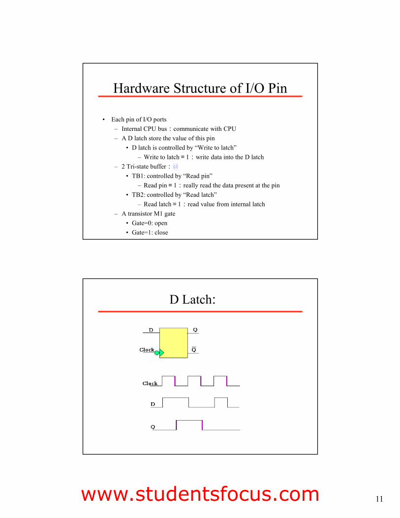
D Latch:
www.studentsfocus.com
12
A Pin of Port 1
8051 IC
D Q
Clk Q
Vcc
Load(L1)
Read latch
Read pin
Write to latch
Internal CPU bus
M1
P1.X pinP1.X
TB1
TB2
P0.x
Writing “1” to Output Pin P1.X
D Q
Clk Q
Vcc
Load(L1)
Read latch
Read pin
Write to latch
Internal CPU bus
M1
P1.X pinP1.X
8051 IC
2. output pin isVcc
1. write a 1 to the pin1
0 output 1
TB1
TB2
www.studentsfocus.com
13
Writing “0” to Output Pin P1.X
D Q
Clk Q
Vcc
Load(L1)
Read latch
Read pin
Write to latch
Internal CPU bus
M1
P1.X pinP1.X
8051 IC
2. output pin is ground
1. write a 0 to the pin0
1 output 0
TB1
TB2
Reading “High” at Input Pin
D Q
Clk Q
Vcc
Load(L1)
Read latch
Read pin
Write to latch
Internal CPU bus
M1
P1.X pin
P1.X
8051 IC
2. MOV A,P1
external pin=High1. write a 1 to the pin MOV
P1,#0FFH
1
0
3. Read pin=1 Read latch=0 Write to latch=1
1
TB1
TB2
www.studentsfocus.com
14
Reading “Low” at Input Pin
D Q
Clk Q
Vcc
Load(L1)
Read latch
Read pin
Write to latch
Internal CPU bus
M1
P1.X pin
P1.X
8051 IC
2. MOV A,P1
external pin=Low1. write a 1 to the pin
MOV P1,#0FFH1
0
3. Read pin=1 Read latch=0 Write to latch=1
0
TB1
TB2
Other Pins
• P1, P2, and P3 have internal pull-up resisters.– P1, P2, and P3 are not open drain.
• P0 has no internal pull-up resistors and does not connects to Vcc inside the 8051.– P0 is open drain.– Compare the figures of P1.X and P0.X. #
• However, for a programmer, it is the same to program P0, P1, P2 and P3.
• All the ports upon RESET are configured as output.
www.studentsfocus.com
15
A Pin of Port 0
8051 IC
D Q
Clk Q
Read latch
Read pin
Write to latch
Internal CPU bus
M1
P0.X pinP1.X
TB1
TB2
P1.x
Port 0 with Pull-Up Resistors
P0.0P0.1P0.2P0.3P0.4P0.5P0.6P0.7
DS500087518951
Vcc10 K
Port
0
www.studentsfocus.com
PERIPHERAL INTERFACING -IV UNIT
MICROPROCESSOR AND MICROCONTROLLER
www.studentsfocus.com
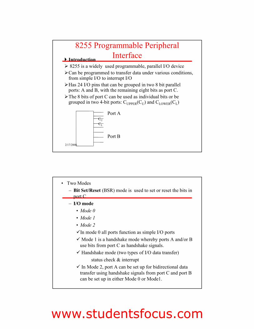
! Introduction! 8255 is a widely used programmable, parallel I/O device!Can be programmed to transfer data under various conditions,
from simple I/O to interrupt I/O!Has 24 I/O pins that can be grouped in two 8 bit parallel
ports: A and B, with the remaining eight bits as port C.!The 8 bits of port C can be used as individual bits or be
grouped in two 4-bit ports: CUPPER(CU) and CLOWER(CL)
Port ACUCL
Port B
8255 Programmable Peripheral Interface
2/17/2008
• Two Modes– Bit Set/Reset (BSR) mode is used to set or reset the bits in
port C– I/O mode
• Mode 0• Mode 1 • Mode 2"In mode 0 all ports function as simple I/O ports" Mode 1 is a handshake mode whereby ports A and/or B
use bits from port C as handshake signals." Handshake mode (two types of I/O data transfer)
status check & interrupt" In Mode 2, port A can be set up for bidirectional data
transfer using handshake signals from port C and port B can be set up in either Mode 0 or Mode1.
www.studentsfocus.com
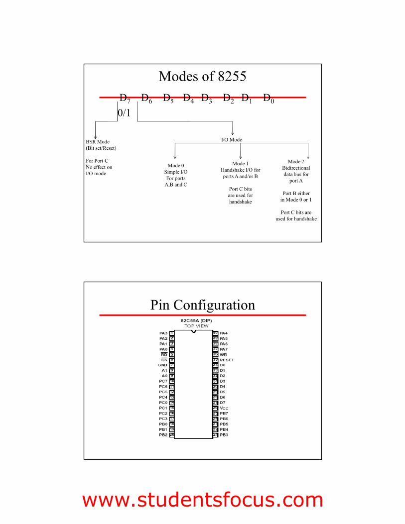
D7 D6 D5 D4 D3 D2 D1 D0
0/1
Modes of 8255
BSR Mode(Bit set/Reset)
For Port CNo effect on I/O mode
I/O Mode
Mode 0Simple I/O For ports
A,B and C
Mode 1Handshake I/O for ports A and/or B
Port C bits are used for handshake
Mode 2Bidirectional data bus for
port A
Port B either in Mode 0 or 1
Port C bits are used for handshake
Pin Configuration
www.studentsfocus.com
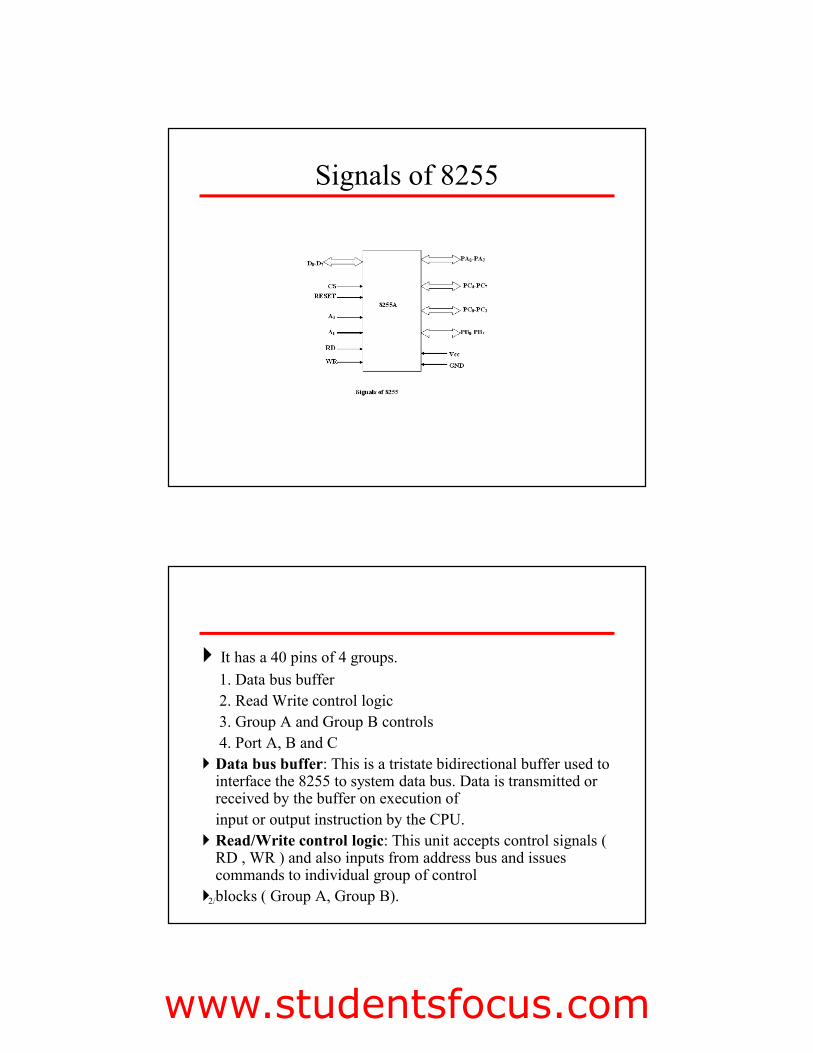
Signals of 8255
! It has a 40 pins of 4 groups.1. Data bus buffer2. Read Write control logic3. Group A and Group B controls4. Port A, B and C
! Data bus buffer: This is a tristate bidirectional buffer used to interface the 8255 to system data bus. Data is transmitted or received by the buffer on execution ofinput or output instruction by the CPU.
! Read/Write control logic: This unit accepts control signals ( RD , WR ) and also inputs from address bus and issues commands to individual group of control
! blocks ( Group A, Group B).2/
www.studentsfocus.com
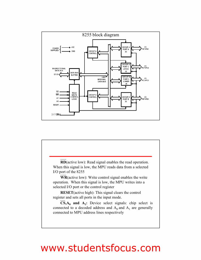
8255 block diagram
2/17/2008
RD(active low): Read signal enables the read operation. When this signal is low, the MPU reads data from a selected I/O port of the 8255
WR(active low): Write control signal enables the write operation. When this signal is low, the MPU writes into a selected I/O port or the control register
RESET(active high): This signal clears the control register and sets all ports in the input mode.
CS,A0 and A1: Device select signals: chip select isconnected to a decoded address and A0 and A1 are generallyconnected to MPU address lines respectively
www.studentsfocus.com
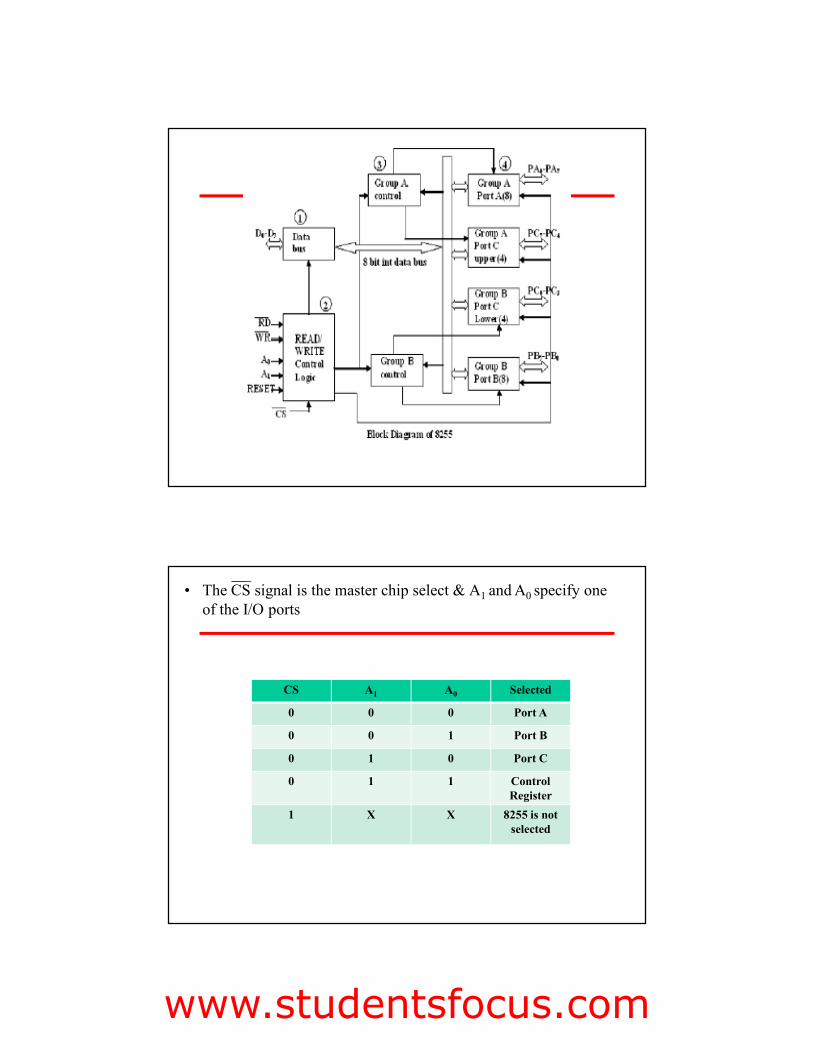
• The CS signal is the master chip select & A1 and A0 specify one of the I/O ports
CS A1 A0 Selected
0 0 0 Port A
0 0 1 Port B
0 1 0 Port C
0 1 1 Control Register
1 X X 8255 is not selected
www.studentsfocus.com
• Group A and Group B controls : These block receive control from the CPU and issues commands to their respective ports.
• Group A - PA and PCU ( PC7 –PC4)
• Group B – PB and PCL ( PC3 – PC0)
• Control word register can only be written into & no read operation of the CW register is allowed.
a) Port A: This has an 8 bit latched/buffered O/P and 8 bit input latch. It can be programmed in 3 modes – mode 0, mode 1, mode 2.
b) Port B: This has an 8 bit latched / buffered O/P and 8 bit input latch. It can be programmed in mode 0, mode1.
c) Port C : This has an 8 bit latched input buffer and 8 bit out put latched/buffer. This port can be divided into two 4 bit ports and can be used as control signals for port A
and port B. it can be programmed in mode 0.
2/17/2008
www.studentsfocus.com
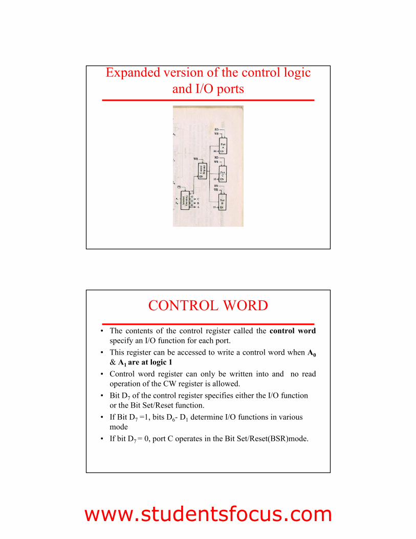
Expanded version of the control logic and I/O ports
• The contents of the control register called the control wordspecify an I/O function for each port.
• This register can be accessed to write a control word when A0& A1 are at logic 1
• Control word register can only be written into and no readoperation of the CW register is allowed.
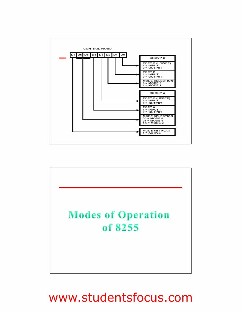
• Bit D7 of the control register specifies either the I/O function or the Bit Set/Reset function.
• If Bit D7 =1, bits D6- D1 determine I/O functions in various mode
• If bit D7 = 0, port C operates in the Bit Set/Reset(BSR)mode.
CONTROL WORD
www.studentsfocus.com
www.studentsfocus.com
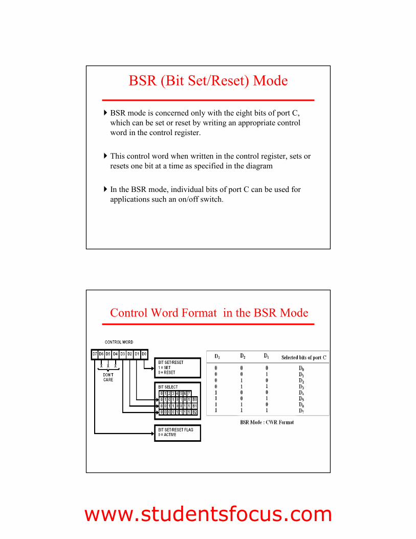
! BSR mode is concerned only with the eight bits of port C, which can be set or reset by writing an appropriate control word in the control register.
! This control word when written in the control register, sets or resets one bit at a time as specified in the diagram
! In the BSR mode, individual bits of port C can be used for applications such an on/off switch.
BSR (Bit Set/Reset) Mode
Control Word Format in the BSR Mode
www.studentsfocus.com
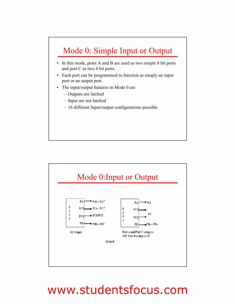
• In this mode, ports A and B are used as two simple 8 bit ports and port C as two 4 bit ports.
• Each port can be programmed to function as simply an input port or an output port.
• The input/output features in Mode 0 are– Outputs are latched– Input are not latched– 16 different Input/output configurations possible
Mode 0: Simple Input or Output
Mode 0:Input or Output
www.studentsfocus.com
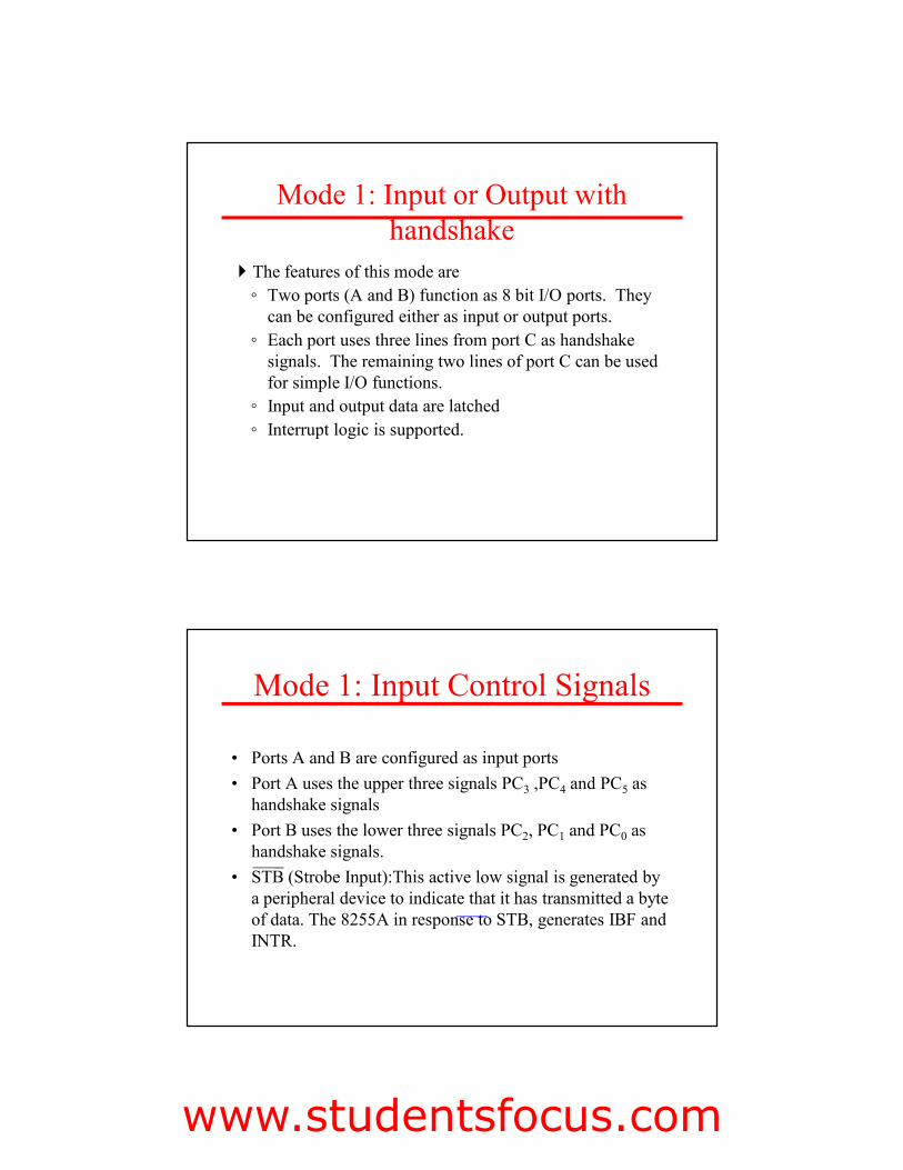
! The features of this mode are◦ Two ports (A and B) function as 8 bit I/O ports. They
can be configured either as input or output ports.◦ Each port uses three lines from port C as handshake
signals. The remaining two lines of port C can be used for simple I/O functions.◦ Input and output data are latched◦ Interrupt logic is supported.
Mode 1: Input or Output with handshake
• Ports A and B are configured as input ports • Port A uses the upper three signals PC3 ,PC4 and PC5 as
handshake signals• Port B uses the lower three signals PC2, PC1 and PC0 as
handshake signals.• STB (Strobe Input):This active low signal is generated by
a peripheral device to indicate that it has transmitted a byte of data. The 8255A in response to STB, generates IBF and INTR.
Mode 1: Input Control Signals
www.studentsfocus.com
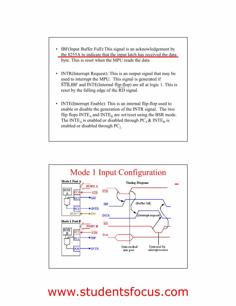
• IBF(Input Buffer Full):This signal is an acknowledgement by the 8255A to indicate that the input latch has received the data byte. This is reset when the MPU reads the data
• INTR(Interrupt Request): This is an output signal that may be used to interrupt the MPU. This signal is generated if STB,IBF and INTE(Internal flip-flop) are all at logic 1. This is reset by the falling edge of the RD signal.
• INTE(Interrupt Enable): This is an internal flip-flop used to enable or disable the generation of the INTR signal. The two flip flops INTEA and INTEB are set/reset using the BSR mode. The INTEA is enabled or disabled through PC4 & INTEB is enabled or disabled through PC2.
Mode 1 Input Configuration
www.studentsfocus.com
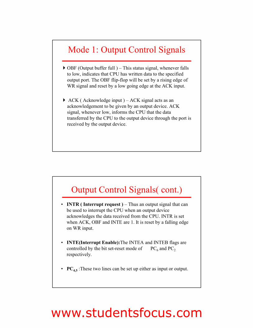
! OBF (Output buffer full ) – This status signal, whenever falls to low, indicates that CPU has written data to the specified output port. The OBF flip-flop will be set by a rising edge of WR signal and reset by a low going edge at the ACK input.
! ACK ( Acknowledge input ) – ACK signal acts as an acknowledgement to be given by an output device. ACK signal, whenever low, informs the CPU that the data transferred by the CPU to the output device through the port is received by the output device.
Mode 1: Output Control Signals
• INTR ( Interrupt request ) – Thus an output signal that can be used to interrupt the CPU when an output device acknowledges the data received from the CPU. INTR is set when ACK, OBF and INTE are 1. It is reset by a falling edge on WR input.
• INTE(Interrupt Enable):The INTEA and INTEB flags are controlled by the bit set-reset mode of PC6 and PC2respectively.
• PC4,5 :These two lines can be set up either as input or output.
Output Control Signals( cont.)
www.studentsfocus.com
2/17/2008
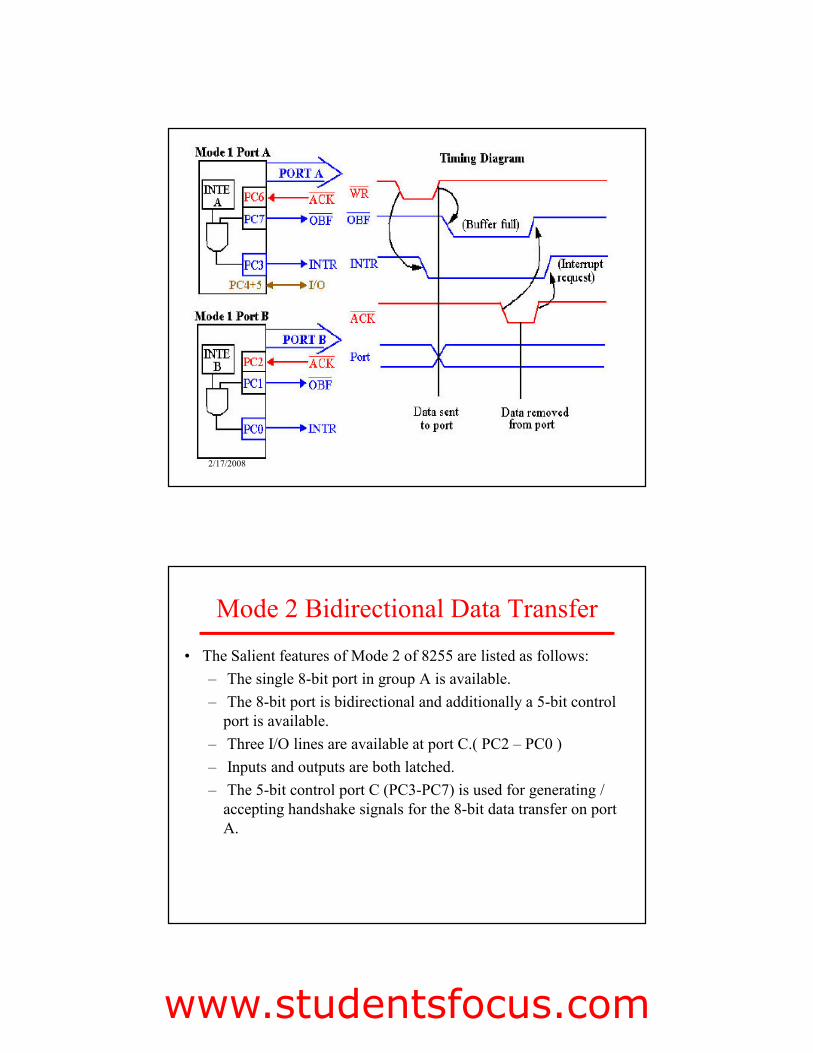
• The Salient features of Mode 2 of 8255 are listed as follows:– The single 8-bit port in group A is available.– The 8-bit port is bidirectional and additionally a 5-bit control
port is available.– Three I/O lines are available at port C.( PC2 – PC0 )– Inputs and outputs are both latched.– The 5-bit control port C (PC3-PC7) is used for generating /
accepting handshake signals for the 8-bit data transfer on port A.
Mode 2 Bidirectional Data Transfer
www.studentsfocus.com
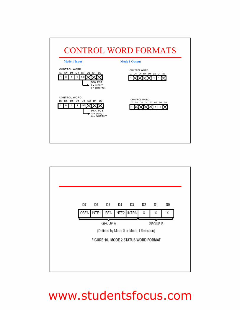
CONTROL WORD FORMATSMode 1 Input Mode 1 Output
www.studentsfocus.com
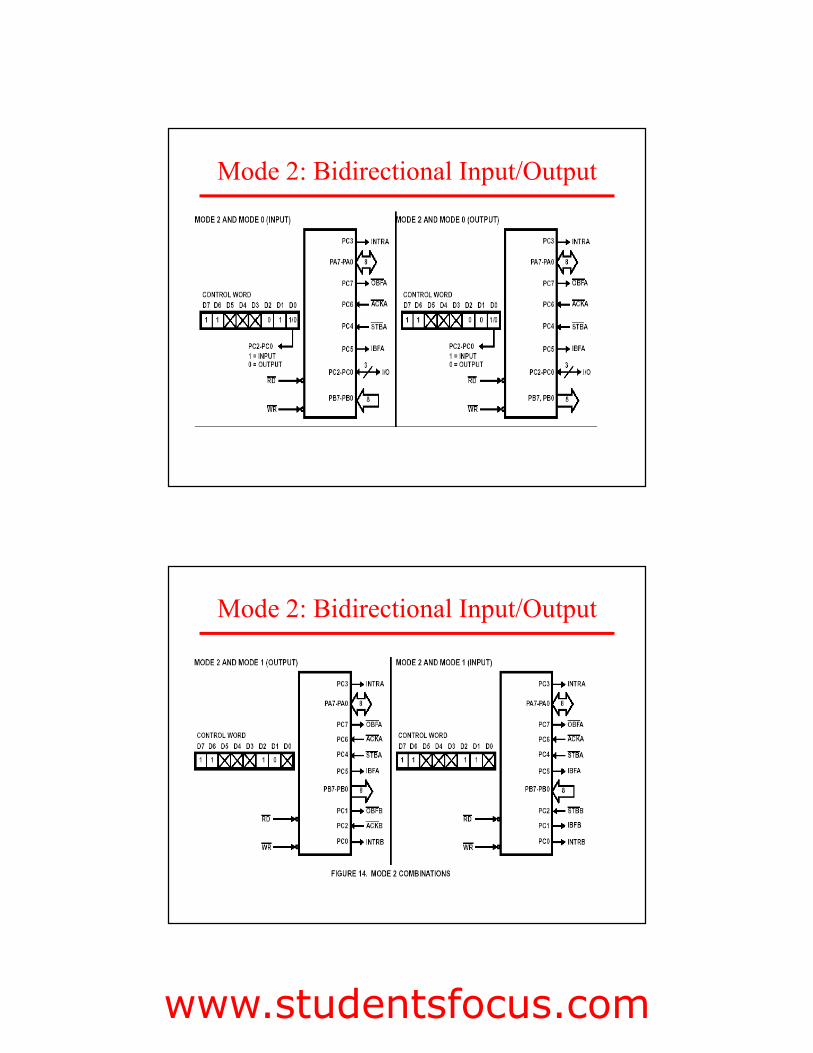
Mode 2: Bidirectional Input/Output
Mode 2: Bidirectional Input/Output
www.studentsfocus.com
• Microprocessor Architecture, Programming and Applications – Ramesh Gaonkar
• Intel 8255 datasheet www.DatasheetCatalog.com
REFERENCES
2/17/2008
www.studentsfocus.com
8254 programmable interval timer/counter
• is functionally similar to software designed counters and timers
• Generates accurate time delays can be used for applications such as a real time clock, event counter, digital one-shot, square wave generator & a complex waveform generator
• Includes 3 identical counters that can operate in any one of 6 modes
Introduction
• A 16 bit count is loaded in its register and, on command, begins to decrement the count until it reaches 0
• At the end of count it generates a pulse that can be used to interrupt the MPU
• The counter can count either in binary or BCD.• 8254 is an upgraded version of 8253 and they are pin-
compatible
Introduction(cont.)
www.studentsfocus.com
• Compatible with All Intel and Most other Microprocessors• Handles Inputs from DC to 2 MHz• 8 MHz 8254• 10 MHz 8254-2• 8254 includes Status Read-Back Command that can latch the
count and the status of the counters.• Single 5V Supply
SPECIFICATIONS
• Three counters (0,1 and2)• Data Bus buffer• Read/Write control logic• Control Register
Each counter has two input signals – clock(CLK) and GATE and one output signal – OUT.
BLOCK DIAGRAM OF 8254
www.studentsfocus.com
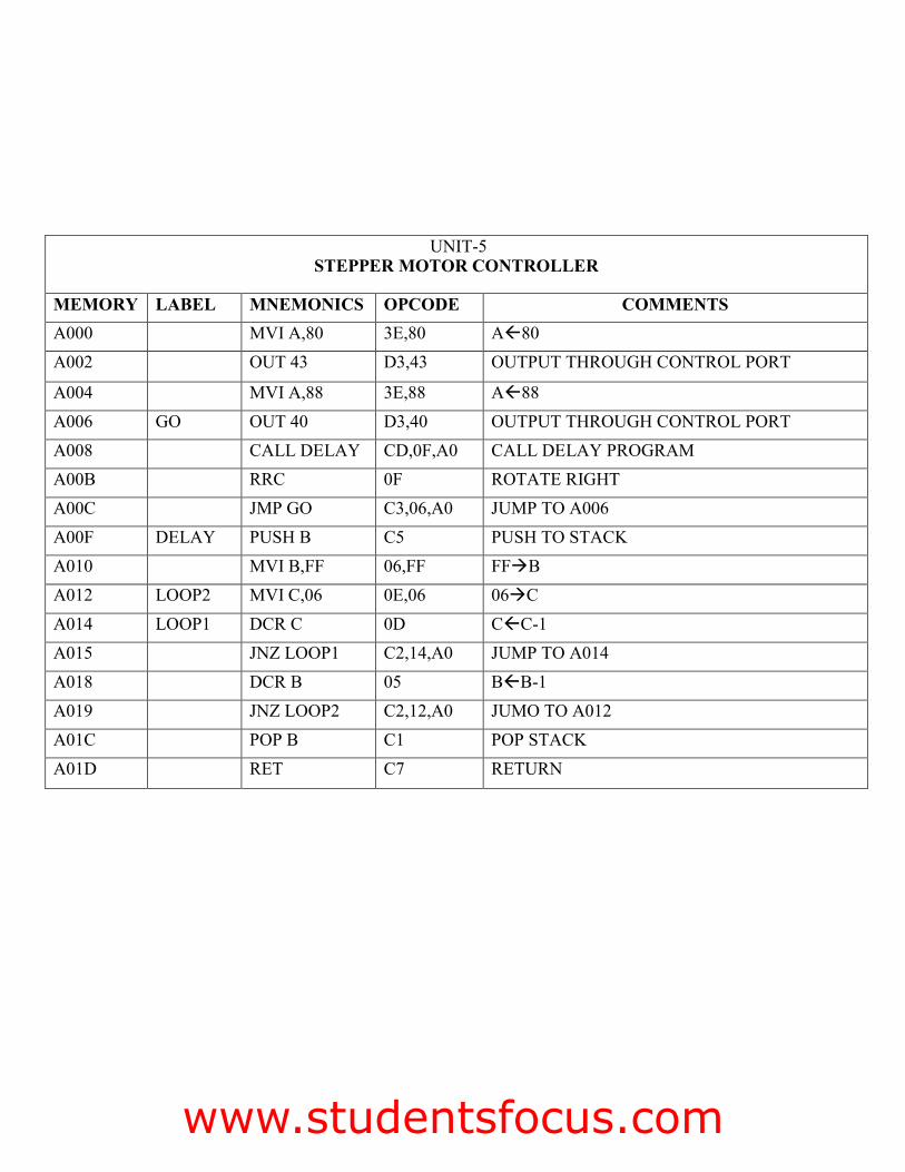
MEMORY LABEL MNEMONICS OPCODE COMMENTS A000 MVI A,80 3E,80 A!80 A002 OUT 43 D3,43 OUTPUT THROUGH CONTROL PORT
A004 MVI A,88 3E,88 A!88 A006 GO OUT 40 D3,40 OUTPUT THROUGH CONTROL PORT A008 CALL DELAY CD,0F,A0 CALL DELAY PROGRAM A00B RRC 0F ROTATE RIGHT A00C JMP GO C3,06,A0 JUMP TO A006 A00F DELAY PUSH B C5 PUSH TO STACK A010 MVI B,FF 06,FF FF"B A012 LOOP2 MVI C,06 0E,06 06"C A014 LOOP1 DCR C 0D C!C-1 A015 JNZ LOOP1 C2,14,A0 JUMP TO A014 A018 DCR B 05 B!B-1 A019 JNZ LOOP2 C2,12,A0 JUMO TO A012 A01C POP B C1 POP STACK A01D RET C7 RETURN
UNIT-5STEPPER MOTOR CONTROLLER
www.studentsfocus.com
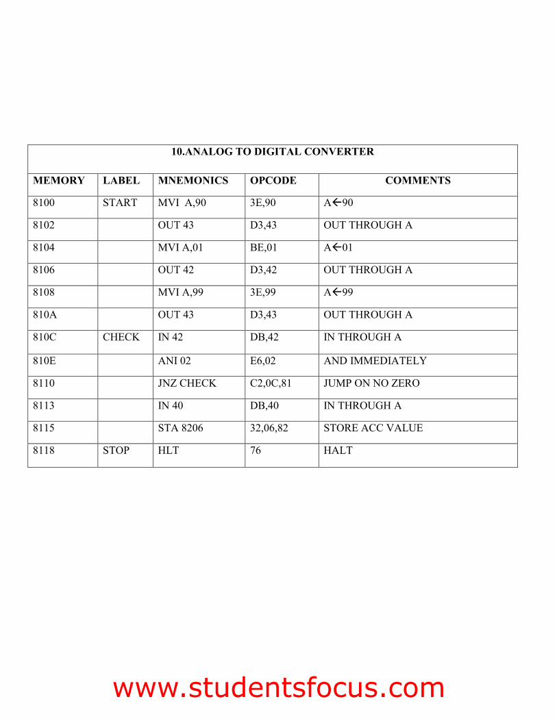
10.ANALOG TO DIGITAL CONVERTER
MEMORY LABEL MNEMONICS OPCODE COMMENTS
8100 START MVI A,90 3E,90 A!90
8102 OUT 43 D3,43 OUT THROUGH A
8104 MVI A,01 BE,01 A!01
8106 OUT 42 D3,42 OUT THROUGH A
8108 MVI A,99 3E,99 A!99
810A OUT 43 D3,43 OUT THROUGH A
810C CHECK IN 42 DB,42 IN THROUGH A
810E ANI 02 E6,02 AND IMMEDIATELY
8110 JNZ CHECK C2,0C,81 JUMP ON NO ZERO
8113 IN 40 DB,40 IN THROUGH A
8115 STA 8206 32,06,82 STORE ACC VALUE
8118 STOP HLT 76 HALT
www.studentsfocus.com
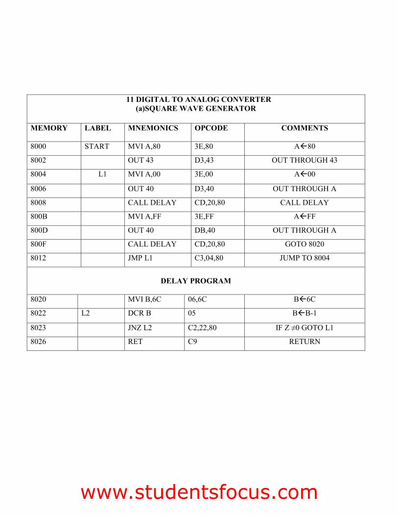
11 DIGITAL TO ANALOG CONVERTER (a)SQUARE WAVE GENERATOR
MEMORY LABEL MNEMONICS OPCODE COMMENTS
8000 START MVI A,80 3E,80 A!80
8002 OUT 43 D3,43 OUT THROUGH 43
8004 L1 MVI A,00 3E,00 A!00
8006 OUT 40 D3,40 OUT THROUGH A
8008 CALL DELAY CD,20,80 CALL DELAY
800B MVI A,FF 3E,FF A!FF
800D OUT 40 DB,40 OUT THROUGH A
800F CALL DELAY CD,20,80 GOTO 8020
8012 JMP L1 C3,04,80 JUMP TO 8004
DELAY PROGRAM
8020 MVI B,6C 06,6C B!6C
8022 L2 DCR B 05 B!B-1
8023 JNZ L2 C2,22,80 IF Z ≠0 GOTO L1
8026 RET C9 RETURN
www.studentsfocus.com
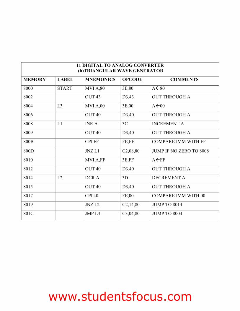
11 DIGITAL TO ANALOG CONVERTER (b)TRIANGULAR WAVE GENERATOR
MEMORY LABEL MNEMONICS OPCODE COMMENTS
8000 START MVI A,80 3E,80 A!80
8002 OUT 43 D3,43 OUT THROUGH A
8004 L3 MVI A,00 3E,00 A!00
8006 OUT 40 D3,40 OUT THROUGH A
8008 L1 INR A 3C INCREMENT A
8009 OUT 40 D3,40 OUT THROUGH A
800B CPI FF FE,FF COMPARE IMM WITH FF
800D JNZ L1 C2,08,80 JUMP IF NO ZERO TO 8008
8010 MVI A,FF 3E,FF A!FF
8012 OUT 40 D3,40 OUT THROUGH A
8014 L2 DCR A 3D DECREMENT A
8015 OUT 40 D3,40 OUT THROUGH A
8017 CPI 40 FE,00 COMPARE IMM WITH 00
8019 JNZ L2 C2,14,80 JUMP TO 8014
801C JMP L3 C3,04,80 JUMP TO 8004
www.studentsfocus.com
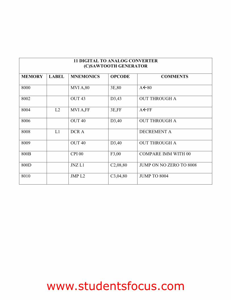
11 DIGITAL TO ANALOG CONVERTER (C)SAWTOOTH GENERATOR
MEMORY LABEL MNEMONICS OPCODE COMMENTS
8000 MVI A,80
3E,80 A!80
8002 OUT 43
D3,43 OUT THROUGH A
8004 L2 MVI A,FF
3E,FF A!FF
8006 OUT 40
D3,40 OUT THROUGH A
8008 L1 DCR A
DECREMENT A
8009 OUT 40
D3,40 OUT THROUGH A
800B CPI 00
F3,00 COMPARE IMM WITH 00
800D JNZ L1
C2,08,80 JUMP ON NO ZERO TO 8008
8010 JMP L2
C3,04,80 JUMP TO 8004
www.studentsfocus.com

www.studentsfocus.com