ee141-spring 2007 digital integrated...
TRANSCRIPT

EE141
1
EE1411
EECS141
EE141EE141--Spring 2007Spring 2007Digital Integrated Digital Integrated CircuitsCircuits
Lecture 14Lecture 14SRAMSRAMProject LaunchProject LaunchLogical EffortLogical Effort
EE1412
EECS141
AnnouncementsAnnouncementsNo new labs next week and week after
Use labs to work on projectHomework #6 due Fr. 5pmProject updated by tomorrow
Proj. Phase 1 due Tu March 20 by 5pmProj. Phase 2 due Tu April 10 by 5pm
Homework #7 posted this weekendDue Fr March 23 by 5pm!
EE141
2
EE1413
EECS141
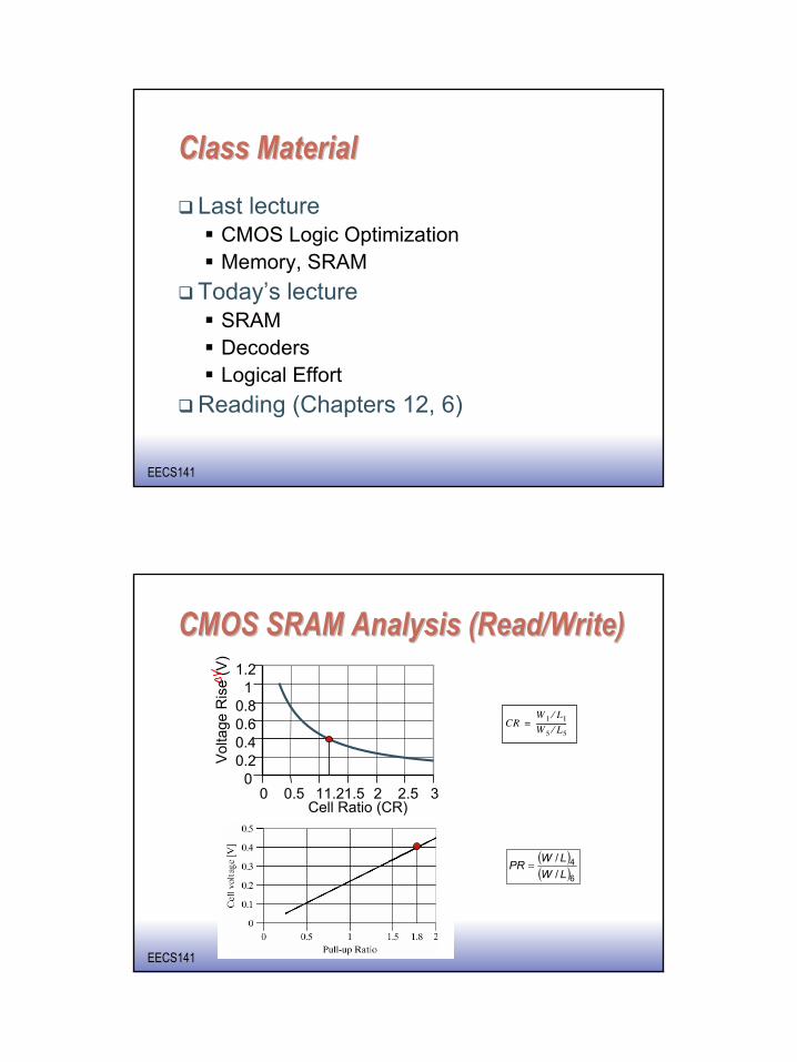
Class MaterialClass MaterialLast lecture
CMOS Logic OptimizationMemory, SRAM
Today’s lectureSRAMDecodersLogical Effort
Reading (Chapters 12, 6)
EE1414
EECS141
CMOS SRAM Analysis (Read/Write)CMOS SRAM Analysis (Read/Write)
V o l t a g e r i s e [ V ]
( )( )6
4//LWLW
PR =
00
0.20.40.60.8
11.2
0.5 11.21.5 2Cell Ratio (CR)
2.5 3
Vol
tage
Ris
e (V
)

EE141
3
EE1415
EECS141
Read Static Noise MarginRead Static Noise Margin
SNM
Obtained by breaking thefeedback between the inverters
EE1416
EECS141
6T6T--SRAM SRAM —— Layout Layout
VDD
GND
WL
BL BLB
Compact cellBitlines: M2Wordline: bootstrapped in M3

EE141
4
EE1417
EECS141
65nm SRAM65nm SRAMST/Philips/Motorola
Access Transistor
Pull down Pull up
EE1418
EECS141
EE141
5
EE1419
EECS141
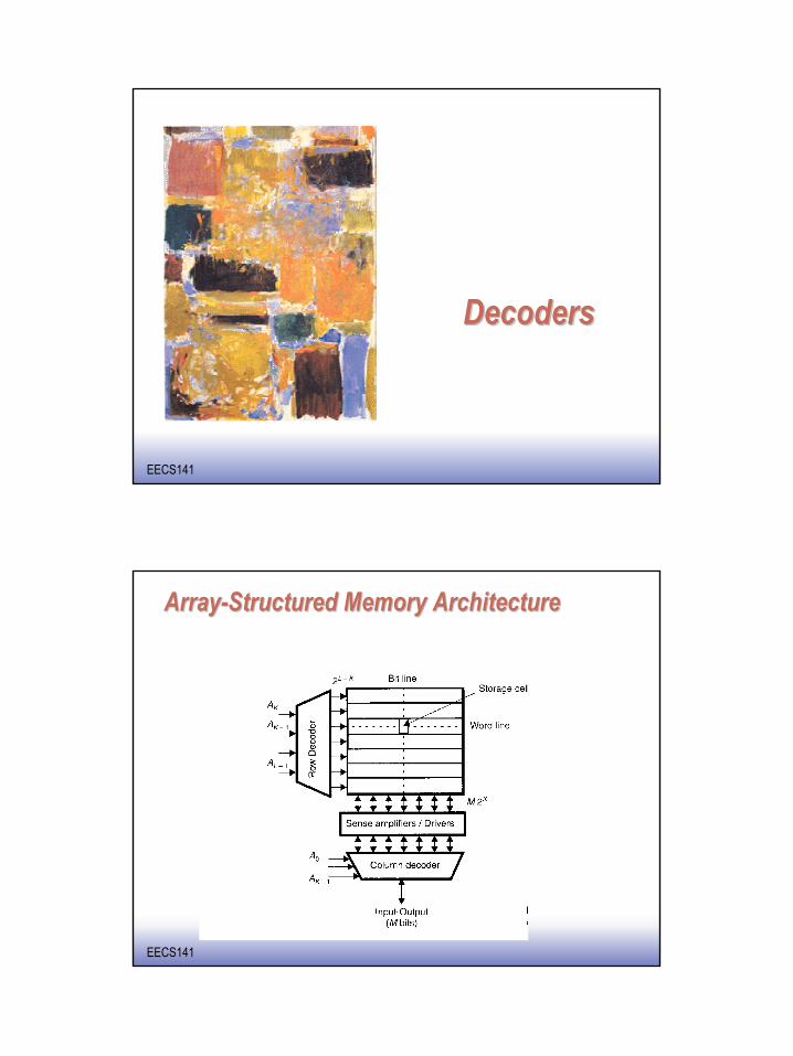
DecodersDecoders
EE14110
EECS141
ArrayArray--Structured Memory ArchitectureStructured Memory Architecture

EE141
6
EE14111
EECS141
Memory Architecture: DecodersMemory Architecture: Decoders
Word 0
Word 1
Word 2
Word N - 2
Word N - 1
Storagecell
M bits M bits
N
w o r d s
S0
S1
S2
SN - 2
A 0
A 1
AK - 1
K = log2N
SN - 1
Word 0
Word 1
Word 2
Word N - 2
Word N - 1
Storagecell
S0
Input-Output(M bits)
Intuitive architecture for N x M memoryToo many select signals:
N words == N select signals K = log2NDecoder reduces the number of select signals
Input-Output(M bits)
D e c o d e r
EE14112
EECS141
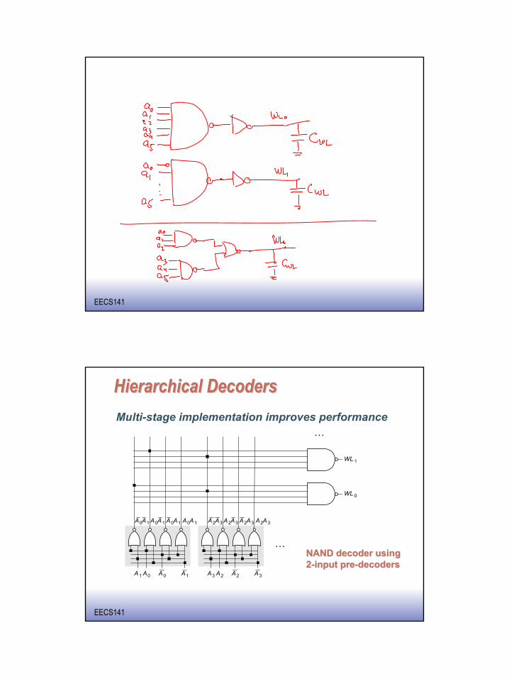
Row DecodersRow DecodersCollection of 2M complex logic gatesOrganized in regular and dense fashion
(N)AND Decoder
NOR Decoder
76543210127
765432100
AAAAAAAAWLAAAAAAAAWL
=
=
( )( )76543210127
765432100
!!
AAAAAAAAWLAAAAAAAAWL
+++++++=
+++++++=
EE141
7
EE14113
EECS141
EE14114
EECS141
Hierarchical DecodersHierarchical Decoders
• • •
• • •
A2A2
A2A3
WL 0
A2A3A2A3A2A3
A3 A3A 0A0
A0A1A0A1A0A1A0A1
A1 A1
WL 1
Multi-stage implementation improves performance
NAND decoder usingNAND decoder using22--input preinput pre--decodersdecoders

EE141
8
EE14115
EECS141
PROJECTPROJECT
EE14116
EECS141
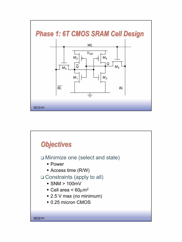
A 64x32 SRAM MemoryA 64x32 SRAM Memory
EE141
9
EE14117
EECS141
Phase 1: 6T CMOS SRAM Cell DesignPhase 1: 6T CMOS SRAM Cell DesignWL
BL
VDD
M5M6
M4
M1
M2
M3
BL
EE14118
EECS141
ObjectivesObjectivesMinimize one (select and state)
PowerAccess time (R/W)
Constraints (apply to all)SNM > 100mVCell area < 60µm2
2.5 V max (no minimum)0.25 micron CMOS
EE141
10
EE14119
EECS141
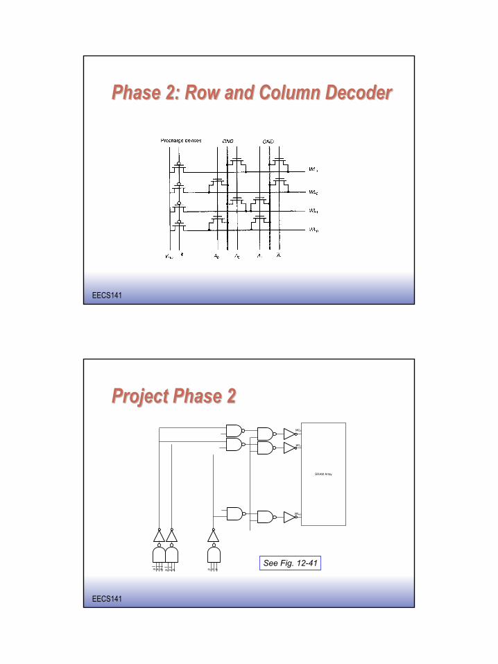
Phase 2: Row and Column DecoderPhase 2: Row and Column Decoder
EE14120
EECS141
Project Phase 2Project Phase 2
SRAM Array
WL0
WL1
WL63
a5 a4 a3 a5 a4 a3 a2 a1 a0
See Fig. 12-41
EE141
11
EE14121
EECS141
EE14122
EECS141
EE141
12
EE14123
EECS141
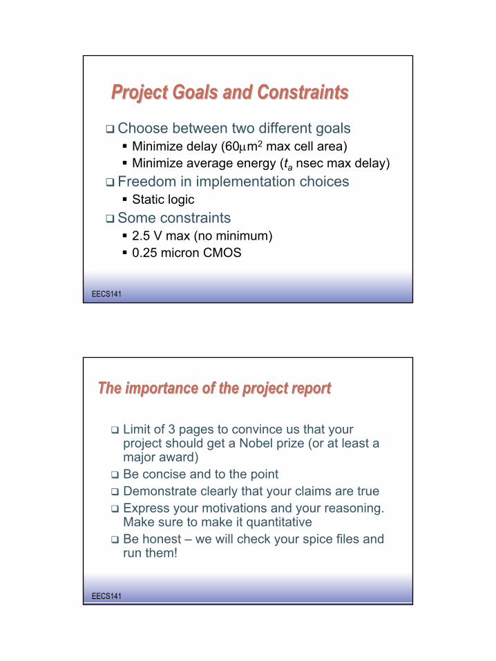
Project Goals and ConstraintsProject Goals and ConstraintsChoose between two different goals
Minimize delay (60µm2 max cell area)Minimize average energy (ta nsec max delay)
Freedom in implementation choicesStatic logic
Some constraints2.5 V max (no minimum)0.25 micron CMOS
EE14124
EECS141
The importance of the project reportThe importance of the project report
Limit of 3 pages to convince us that your project should get a Nobel prize (or at least a major award)Be concise and to the pointDemonstrate clearly that your claims are trueExpress your motivations and your reasoning. Make sure to make it quantitativeBe honest – we will check your spice files and run them!

EE141
13
EE14125
EECS141
Recommended ReadingRecommended Reading
Chapter 6 and 12
EE14126
EECS141
Other recommendationsOther recommendations
Do not start with “optimization by simulation”Think through the problem first and build a first-order analytical model to startDO NOT FORGET WIRING

EE141
14
EE14127
EECS141
Logical Logical EffortEffort
EE14128
EECS141
Sizing Logic Paths for SpeedSizing Logic Paths for SpeedFrequently, input capacitance of a logic path is constrainedLogic has to drive some capacitanceExample: ALU load in an Intel’s microprocessor is 0.5pFHow do we size the ALU datapath to achieve maximum speed?We have already solved this for the inverter chain – can we generalize it for any type of logic?
EE141
15
EE14129
EECS141
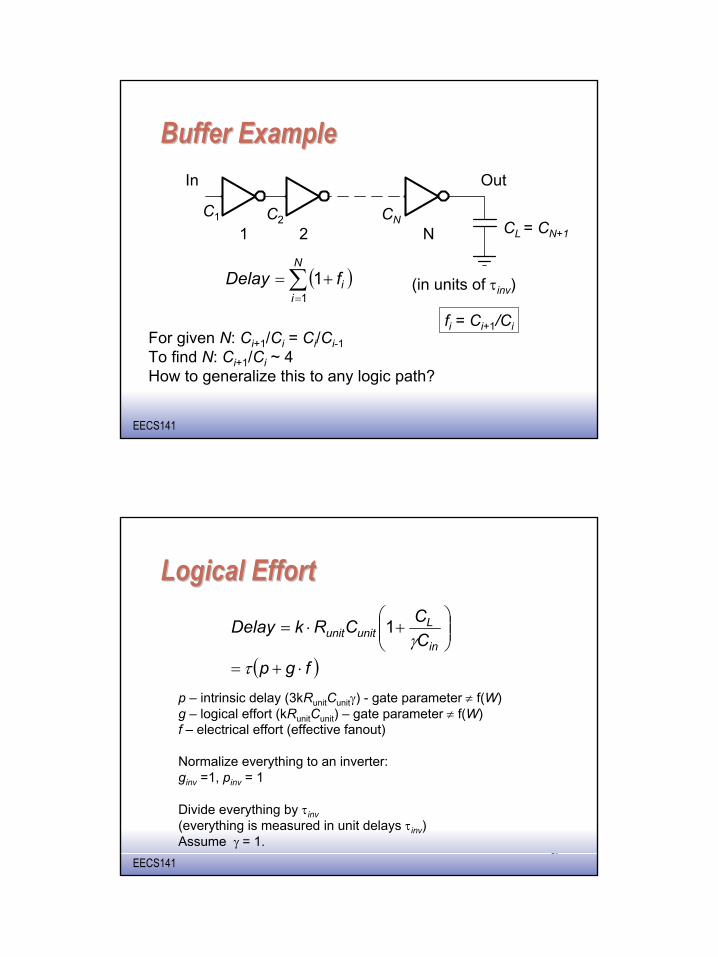
Buffer ExampleBuffer Example
( )∑=
+=N
iifDelay
11
For given N: Ci+1/Ci = Ci/Ci-1To find N: Ci+1/Ci ~ 4How to generalize this to any logic path?
CL = CN+1
In Out
1 2 N
(in units of τinv)
fi = Ci+1/Ci
C1 C2 CN
EE14130
EECS141
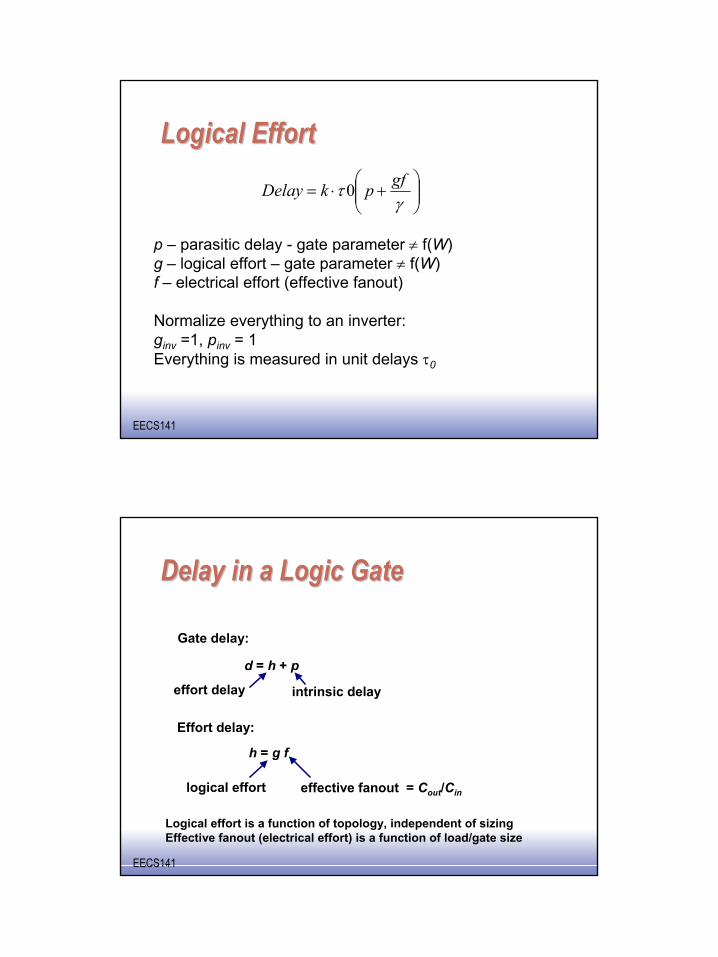
Logical EffortLogical Effort
( )fgpCCCRkDelay
in
Lunitunit
⋅+=
+⋅=
τγ
1
p – intrinsic delay (3kRunitCunitγ) - gate parameter ≠ f(W)g – logical effort (kRunitCunit) – gate parameter ≠ f(W)f – electrical effort (effective fanout)
Normalize everything to an inverter:ginv =1, pinv = 1
Divide everything by τinv(everything is measured in unit delays τinv)Assume γ = 1.
EE141
16
EE14131
EECS141
Logical EffortLogical Effort
+⋅=
γτ gfpkDelay 0
p – parasitic delay - gate parameter ≠ f(W)g – logical effort – gate parameter ≠ f(W)f – electrical effort (effective fanout)
Normalize everything to an inverter:ginv =1, pinv = 1Everything is measured in unit delays τ0
EE14132
EECS141
Delay in a Logic GateDelay in a Logic Gate
Gate delay:
d = h + p
effort delay intrinsic delay
Effort delay:
h = g f
logical effort effective fanout = Cout/Cin
Logical effort is a function of topology, independent of sizingEffective fanout (electrical effort) is a function of load/gate size

EE141
17
EE14133
EECS141
Logical EffortLogical EffortInverter has the smallest logical effort and intrinsic delay of all static CMOS gatesLogical effort of a gate presents the ratio of its input capacitance to the inverter capacitance when sized to deliver the same currentLogical effort increases with the gate complexity
EE14134
EECS141
Logical EffortLogical EffortLogical effort is the ratio of input capacitance of a gate (input) to the input capacitance of an inverter with the same output current
g = 1 g = 4/3 g = 5/3
B
A
A B
F
VDDVDD
A B
A
B
F
VDD
A
A
F
1
2 2 2
2
21 1
4
4
Inverter 2-input NAND 2-input NOR
EE141
18
EE14135
EECS141
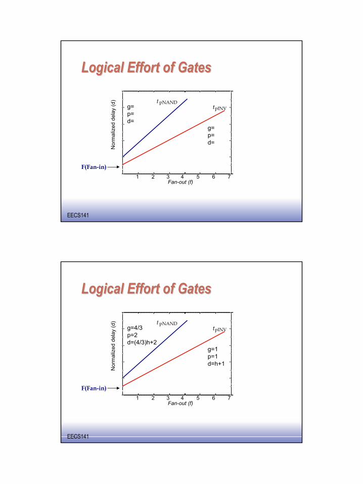
Logical Effort of GatesLogical Effort of Gates
Fan-out (f)
Nor
mal
ized
del
ay (d
)t
1 2 3 4 5 6 7
pINVtpNAND
F(Fan-in)
g=p=d=
g=p=d=
EE14136
EECS141
Logical Effort of GatesLogical Effort of Gates
Fan-out (f)
Nor
mal
ized
del
ay (d
)
t
1 2 3 4 5 6 7
pINVtpNAND
F(Fan-in)
g=1p=1d=h+1
g=4/3p=2d=(4/3)h+2

EE141
19
EE14137
EECS141
Logical Effort of GatesLogical Effort of Gates
�IntrinsicDelay
EffortDelay
1 2 3 4 5Fanout f
1
2
3
4
5
Inverter:g =
1; p = 1
2-inp
ut NAND: g
= 4/3;p =
2
Nor
mal
ized
Del
ay
EE14138
EECS141
Add Branching EffortAdd Branching Effort
Branching effort:
pathon
pathoffpathon
CCC
b−
−− +=
Coff-path
Con-path
EE141
20
EE14139
EECS141
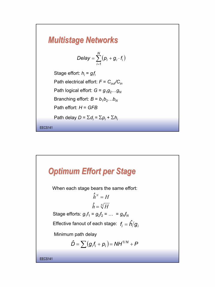
Multistage NetworksMultistage Networks
Stage effort: hi = gifiPath electrical effort: F = Cout/Cin
Path logical effort: G = g1g2…gN
Branching effort: B = b1b2…bN
Path effort: H = GFB
Path delay D = Σdi = Σpi + Σhi
( )∑=
⋅+=N
iiii fgpDelay
1
EE14140
EECS141
Optimum Effort per StageOptimum Effort per Stage
HhN =
When each stage bears the same effort:
N Hh =
( ) PNHpfgD Niii +=+= ∑ /1ˆ
Minimum path delay
Effective fanout of each stage: ii ghf =
Stage efforts: g1f1 = g2f2 = … = gNfN

EE141
21
EE14141
EECS141
Optimal Number of StagesOptimal Number of StagesFor a given load, and given input capacitance of the first gateFind optimal number of stages and optimal sizing
∑+= iN pNHD /1
NHh ˆ/1=The ‘best stage effort’
Remember: we can always add inverters to the end of the chain
is around 4 (3.6 with γ=1)
EE14142
EECS141
Logical EffortLogical Effort
From Sutherland, Sproull

EE141
22
EE14143
EECS141
Example: Optimize PathExample: Optimize Path
Effective fanout, F =G = H =h =a =b =
1a
b c5
g = 1f = a
g = 5/3f = b/a
g = 5/3f = c/b
g = 1f = 5/c
EE14144
EECS141
Example: Optimize PathExample: Optimize Path1
ab c
5
g = 1f = a
g = 5/3f = b/a
g = 5/3f = c/b
g = 1f = 5/c
Effective fanout, F = 5G = 25/9H = 125/9 = 13.9h = 1.93a = 1.93b = ha/g2 = 2.23c = hb/g3 = 5g4/f = 2.59

EE141
23
EE14145
EECS141
Example Example –– 88--Input ANDInput AND
EE14146
EECS141
Next LectureNext Lecture
Logical Effort Wrap-upRatioed LogicPass-Transistor Logic